256-position i c -compatible digital potentiometer ad5245 · 256-position i2c®-compatible digital...
TRANSCRIPT
256-Position I2C®-Compatible Digital Potentiometer
AD5245
Rev. B Information furnished by Analog Devices is believed to be accurate and reliable. However, no responsibility is assumed by Analog Devices for its use, nor for any infringements of patents or other rights of third parties that may result from its use. Specifications subject to change without notice. No license is granted by implication or otherwise under any patent or patent rights of Analog Devices. Trademarks and registered trademarks are the property of their respective owners.
One Technology Way, P.O. Box 9106, Norwood, MA 02062-9106, U.S.A.Tel: 781.329.4700 www.analog.com Fax: 781.461.3113 ©2006 Analog Devices, Inc. All rights reserved.
FEATURES 256-position End-to-end resistance 5 kΩ, 10 kΩ, 50 kΩ, 100 kΩ Compact SOT-23-8 (2.9 mm × 3 mm) package Fast settling time: tS = 5 µs typ on power-up Full read/write of wiper register Power-on preset to midscale Extra package address decode pin AD0 Computer software replaces µC in factory programming
applications Single supply: 2.7 V to 5.5 V Low temperature coefficient 45 ppm/°C Low power: IDD = 8 µA Wide operating temperature: –40°C to +125°C Evaluation board available
APPLICATIONS Mechanical potentiometer replacement in new designs LCD panel VCOM adjustment LCD panel brightness and contrast control Transducer adjustment of pressure, temperature, position,
chemical, and optical sensors RF amplifier biasing Automotive electronics adjustment Gain control and offset adjustment
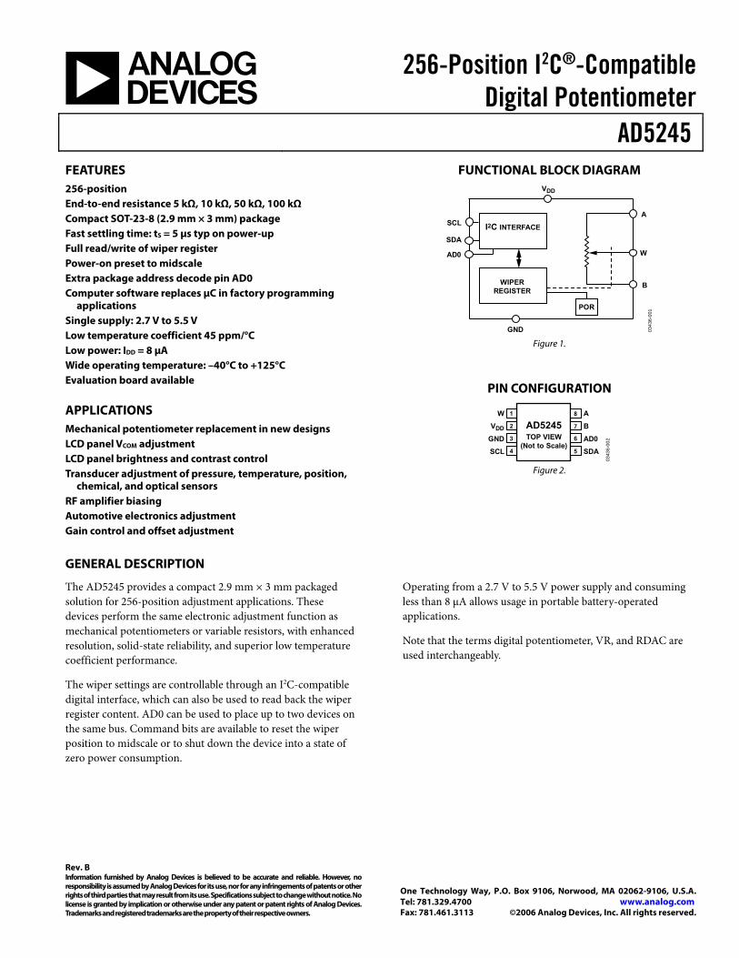
FUNCTIONAL BLOCK DIAGRAM
I2C INTERFACE
WIPERREGISTER
SCL
SDA
AD0
GND
VDD
A
W
B
POR
0343
6-00
1
Figure 1.
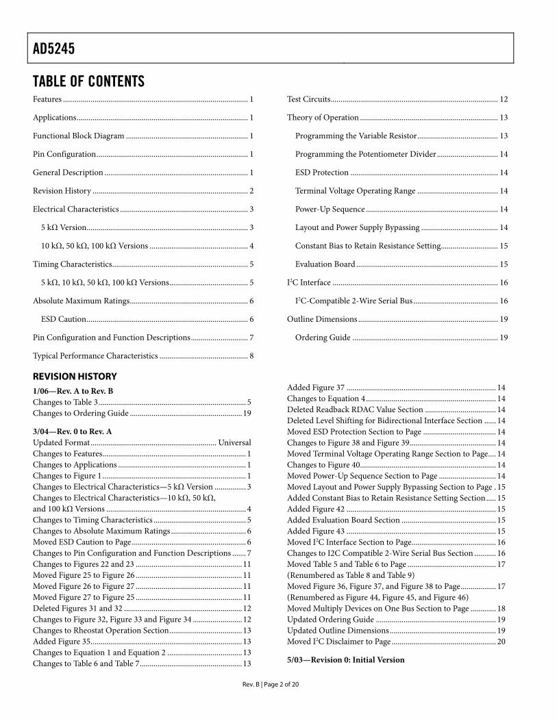
PIN CONFIGURATION
A
B
AD0
SDA
1
2
3
4 5
8
7
6
W
VDD
GND
SCL
AD5245TOP VIEW
(Not to Scale)
0343
6-00
2
Figure 2.
GENERAL DESCRIPTION
The AD5245 provides a compact 2.9 mm × 3 mm packaged solution for 256-position adjustment applications. These devices perform the same electronic adjustment function as mechanical potentiometers or variable resistors, with enhanced resolution, solid-state reliability, and superior low temperature coefficient performance.
The wiper settings are controllable through an I2C-compatible digital interface, which can also be used to read back the wiper register content. AD0 can be used to place up to two devices on the same bus. Command bits are available to reset the wiper position to midscale or to shut down the device into a state of zero power consumption.
Operating from a 2.7 V to 5.5 V power supply and consuming less than 8 µA allows usage in portable battery-operated applications.
Note that the terms digital potentiometer, VR, and RDAC are used interchangeably.
AD5245
Rev. B | Page 2 of 20
TABLE OF CONTENTS Features .............................................................................................. 1
Applications....................................................................................... 1
Functional Block Diagram .............................................................. 1
Pin Configuration............................................................................. 1
General Description ......................................................................... 1
Revision History ............................................................................... 2
Electrical Characteristics ................................................................. 3
5 kΩ Version.................................................................................. 3
10 kΩ, 50 kΩ, 100 kΩ Versions .................................................. 4
Timing Characteristics..................................................................... 5
5 kΩ, 10 kΩ, 50 kΩ, 100 kΩ Versions........................................ 5
Absolute Maximum Ratings............................................................ 6
ESD Caution.................................................................................. 6
Pin Configuration and Function Descriptions............................. 7
Typical Performance Characteristics ............................................. 8
Test Circuits..................................................................................... 12
Theory of Operation ...................................................................... 13
Programming the Variable Resistor......................................... 13
Programming the Potentiometer Divider............................... 14
ESD Protection ........................................................................... 14
Terminal Voltage Operating Range ......................................... 14
Power-Up Sequence ................................................................... 14
Layout and Power Supply Bypassing ....................................... 14
Constant Bias to Retain Resistance Setting............................. 15
Evaluation Board ........................................................................ 15
I C Interface2 .................................................................................... 16
I C-Compatible 2-Wire Serial Bus2 ........................................... 16
Outline Dimensions ....................................................................... 19
Ordering Guide .......................................................................... 19
REVISION HISTORY1/06—Rev. A to Rev. B Changes to Table 3........................................................................... 5 Changes to Ordering Guide .........................................................19
3/04—Rev. 0 to Rev. A Updated Format................................................................ Universal Changes to Features......................................................................... 1 Changes to Applications ................................................................. 1 Changes to Figure 1......................................................................... 1 Changes to Electrical Characteristics—5 kΩ Version ................ 3 Changes to Electrical Characteristics—10 kΩ, 50 kΩ, and 100 kΩ Versions ....................................................................... 4 Changes to Timing Characteristics ............................................... 5 Changes to Absolute Maximum Ratings ...................................... 6 Moved ESD Caution to Page .......................................................... 6 Changes to Pin Configuration and Function Descriptions ....... 7 Changes to Figures 22 and 23 ......................................................11 Moved Figure 25 to Figure 26 ......................................................11 Moved Figure 26 to Figure 27 ......................................................11 Moved Figure 27 to Figure 25 ......................................................11 Deleted Figures 31 and 32 ............................................................12 Changes to Figure 32, Figure 33 and Figure 34 .........................12 Changes to Rheostat Operation Section.....................................13 Added Figure 35.............................................................................13 Changes to Equation 1 and Equation 2 ......................................13 Changes to Table 6 and Table 7....................................................13
Added Figure 37 ............................................................................ 14 Changes to Equation 4 .................................................................. 14 Deleted Readback RDAC Value Section .................................... 14 Deleted Level Shifting for Bidirectional Interface Section ...... 14 Moved ESD Protection Section to Page ..................................... 14 Changes to Figure 38 and Figure 39............................................ 14 Moved Terminal Voltage Operating Range Section to Page.... 14 Changes to Figure 40..................................................................... 14 Moved Power-Up Sequence Section to Page ............................. 14 Moved Layout and Power Supply Bypassing Section to Page . 15 Added Constant Bias to Retain Resistance Setting Section..... 15 Added Figure 42 ............................................................................ 15 Added Evaluation Board Section ................................................ 15 Added Figure 43 ............................................................................ 15 Moved I2C Interface Section to Page........................................... 16 Changes to I2C Compatible 2-Wire Serial Bus Section ........... 16 Moved Table 5 and Table 6 to Page ............................................. 17 (Renumbered as Table 8 and Table 9) Moved Figure 36, Figure 37, and Figure 38 to Page.................. 17 (Renumbered as Figure 44, Figure 45, and Figure 46) Moved Multiply Devices on One Bus Section to Page ............. 18 Updated Ordering Guide ............................................................. 19 Updated Outline Dimensions...................................................... 19 Moved I2C Disclaimer to Page ..................................................... 20
5/03—Revision 0: Initial Version
AD5245
Rev. B | Page 3 of 20
ELECTRICAL CHARACTERISTICS 5 kΩ VERSION VDD = 5 V ± 10% or 3 V ± 10%, VA = VDD, VB = 0 V, –40°C < TA < +125°C, unless otherwise noted.
Table 1. Parameter Symbol Conditions Min Typ1 Max Unit DC CHARACTERISTICS—RHEOSTAT MODE
Resistor Differential Nonlinearity2 R-DNL RWB, VA = no connect –1.5 ±0.1 +1.5 LSB Resistor Integral Nonlinearity2 R-INL RWB, VA = no connect –4 ±0.75 +4 LSB Nominal Resistor Tolerance3 ∆RAB TA = 25°C –30 +30 % Resistance Temperature Coefficient (∆RAB/RAB)/∆T × 106 VAB = VDD, wiper = no connect 45 ppm/°C Wiper Resistance RW 50 120 Ω
DC CHARACTERISTICS—POTENTIOMETER DIVIDER MODE (Specifications Apply to All VRs) Differential Nonlinearity4 DNL –1.5 ±0.1 +1.5 LSB Integral Nonlinearity4 INL –1.5 ±0.6 +1.5 LSB Voltage Divider Temperature Coefficient (∆VW/VW)/∆T × 106 Code = 0x80 15 ppm/°C Full-Scale Error VWFSE Code = 0xFF –6 –2.5 0 LSB Zero-Scale Error VWZSE Code = 0x00 0 2 6 LSB
RESISTOR TERMINALS Voltage Range5 VA, VB, VW GND VDD V
Capacitance A, B6 CA, CB
f = 1 MHz, measured to GND, code = 0x80 90 pF
Capacitance W6 CW
f = 1 MHz, measured to GND, code = 0x80 95 pF
Shutdown Supply Current7 IA_SD VDD = 5.5 V 0.01 1 µA Common-Mode Leakage ICM VA = VB = VDD/2 1 nA
DIGITAL INPUTS AND OUTPUTS Input Logic High VIH VDD = 5 V 2.4 V Input Logic Low VIL VDD = 5 V 0.8 V Input Logic High VIH VDD = 3 V 2.1 V Input Logic Low VIL VDD = 3 V 0.6 V Input Current IIL VIN = 0 V or 5 V ±1 µA Input Capacitance6 CIL 5 pF
POWER SUPPLIES Power Supply Range VDD RANGE 2.7 5.5 V Supply Current IDD VIH = 5 V or VIL = 0 V 3 8 µA Power Dissipation8 PDISS VIH = 5 V or VIL = 0 V, VDD = 5 V 44 µW Power Supply Sensitivity PSS VDD = +5 V ± 10%, code = midscale ±0.02 ±0.05 %/%
DYNAMIC CHARACTERISTICS6, 9 Bandwidth –3 dB BW_5K RAB = 5 kΩ, code = 0x80 1.2 MHz Total Harmonic Distortion THDW VA = 1 V rms, VB = 0 V, f = 1 kHz 0.1 % VW Settling Time tS VA = 5 V, VB = 0 V, ±1 LSB error band 1 µs Resistor Noise Voltage Density eN_WB RWB = 2.5 kΩ, RS = 0 6 nV/√Hz
1 Typical specifications represent average readings at 25°C and VDD = 5 V. 2 Resistor position nonlinearity error R-INL is the deviation from an ideal value measured between the maximum resistance and the minimum resistance wiper
positions. R-DNL measures the relative step change from ideal between successive tap positions. Parts are guaranteed monotonic. 3 VAB = VDD, wiper (VW) = no connect. 4 INL and DNL are measured at VW with the RDAC configured as a potentiometer divider similar to a voltage output D/A converter. VA = VDD and VB = 0 V.
DNL specification limits of ±1 LSB maximum are guaranteed monotonic operating conditions. 5 Resistor Terminals A, B, and W have no limitations on polarity with respect to each other. 6 Guaranteed by design and not subject to production test. 7 Measured at the A terminal. The A terminal is open circuited in shutdown mode. 8 PDISS is calculated from (IDD × VDD). CMOS logic level inputs result in minimum power dissipation. 9 All dynamic characteristics use VDD = 5 V.
AD5245
Rev. B | Page 4 of 20
10 kΩ, 50 kΩ, 100 kΩ VERSIONS VDD = 5 V ± 10% or 3 V ± 10%, VA = VDD, VB = 0 V, –40°C < TA < +125°C, unless otherwise noted.
Table 2. Parameter Symbol Conditions Min Typ1 Max Unit DC CHARACTERISTICS—RHEOSTAT MODE
Resistor Differential Nonlinearity2 R-DNL RWB, VA = no connect –1 ±0.1 +1 LSB Resistor Integral Nonlinearity2 R-INL RWB, VA = no connect –2 ±0.25 +2 LSB Nominal Resistor Tolerance3 ∆RAB TA = 25°C –30 +30 % Resistance Temperature Coefficient (∆RAB/RAB)/∆T × 106 VAB = VDD, wiper = no connect 45 ppm/°C Wiper Resistance RW VDD = 5 V 50 120 Ω
DC CHARACTERISTICS—POTENTIOMETER DIVIDER MODE (Specifications Apply to All VRs) Differential Nonlinearity4 DNL –1 ±0.1 +1 LSB Integral Nonlinearity4 INL –1 ±0.3 +1 LSB Voltage Divider Temperature Coefficient (∆VW/VW)/∆T × 106 Code = 0x80 15 ppm/°C Full-Scale Error VWFSE Code = 0xFF –3 –1 0 LSB Zero-Scale Error VWZSE Code = 0x00 0 1 3 LSB
RESISTOR TERMINALS Voltage Range5 VA, VB, VW GND VDD V Capacitance A, B6 CA, CB f = 1 MHz, measured to GND,
code = 0x80 90 pF
Capacitance W6 CW f = 1 MHz, measured to GND, code = 0x80
95 pF
Shutdown Supply Current IA_SD VDD = 5.5 V 0.01 1 µA Common-Mode Leakage ICM VA = VB = VDD/2 1 nA
DIGITAL INPUTS AND OUTPUTS Input Logic High VIH VDD = 5 V 2.4 V Input Logic Low VIL VDD = 5 V 0.8 V Input Logic High VIH VDD = 3 V 2.1 V Input Logic Low VIL VDD = 3 V 0.6 V Input Current IIL VIN = 0 V or 5 V ±1 µA Input Capacitance6 CIL 5 pF
POWER SUPPLIES Power Supply Range VDD RANGE 2.7 5.5 V Supply Current IDD VIH = 5 V or VIL = 0 V 3 8 µA Power Dissipation7 PDISS VIH = 5 V or VIL = 0 V, VDD = 5 V 44 µW Power Supply Sensitivity PSS VDD = 5 V ± 10%,
code = midscale ±0.02 ±0.05 %/%
DYNAMIC CHARACTERISTICS6, 8 Bandwidth –3 dB BW RAB = 10 kΩ/50 kΩ/100 kΩ,
code = 0x80 600/100/40 kHz
Total Harmonic Distortion THDW VA = 1 V rms, VB = 0 V, f = 1 kHz, RAB = 10 kΩ
0.1 %
VW Settling Time (10 kΩ/50 kΩ/100 kΩ) tS VA = 5 V, VB = 0 V, ±1 LSB error band
2 µs
Resistor Noise Voltage Density eN_WB RWB = 5 kΩ, RS = 0 9 nV/√Hz 1 Typical specifications represent average readings at 25°C and VDD = 5 V. 2 Resistor position nonlinearity error R-INL is the deviation from an ideal value measured between the maximum resistance and the minimum resistance wiper
positions. R-DNL measures the relative step change from ideal between successive tap positions. Parts are guaranteed monotonic. 3 VAB = VDD, wiper (VW) = no connect. 4 INL and DNL are measured at VW with the RDAC configured as a potentiometer divider similar to a voltage output D/A converter. VA = VDD and VB = 0 V.
DNL specification limits of ±1 LSB maximum are guaranteed monotonic operating conditions. 5 Resistor Terminals A, B, W have no limitations on polarity with respect to each other. 6 Guaranteed by design and not subject to production test. 7 PDISS is calculated from (IDD × VDD). CMOS logic level inputs result in minimum power dissipation. 8 All dynamic characteristics use VDD = 5 V.
AD5245
Rev. B | Page 5 of 20
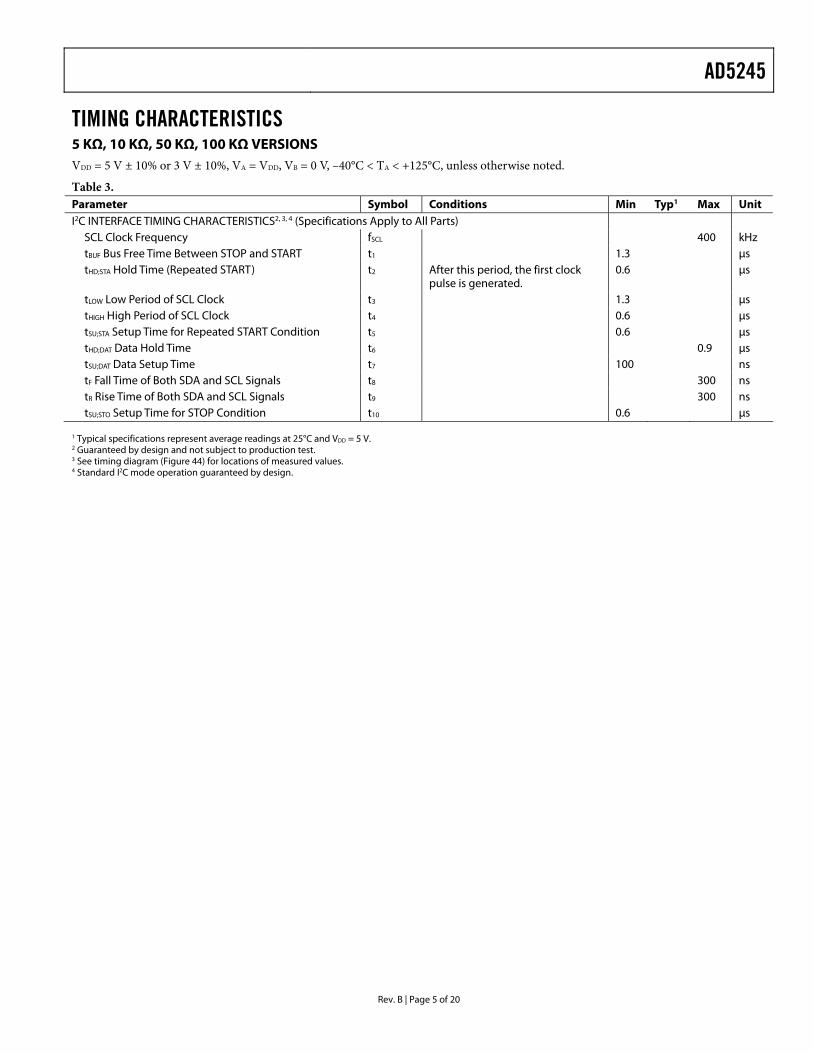
TIMING CHARACTERISTICS 5 KΩ, 10 KΩ, 50 KΩ, 100 KΩ VERSIONS VDD = 5 V ± 10% or 3 V ± 10%, VA = VDD, VB = 0 V, –40°C < TA < +125°C, unless otherwise noted.
Table 3. Parameter Symbol Conditions Min Typ1 Max Unit I2C INTERFACE TIMING CHARACTERISTICS2, , 3 4 (Specifications Apply to All Parts)
SCL Clock Frequency fSCL 400 kHz tBUF Bus Free Time Between STOP and START t1 1.3 µs tHD;STA Hold Time (Repeated START) t2 After this period, the first clock
pulse is generated. 0.6 µs
tLOW Low Period of SCL Clock t3 1.3 µs tHIGH High Period of SCL Clock t4 0.6 µs tSU;STA Setup Time for Repeated START Condition t5 0.6 µs tHD;DAT Data Hold Time t6 0.9 µs tSU;DAT Data Setup Time t7 100 ns tF Fall Time of Both SDA and SCL Signals t8 300 ns tR Rise Time of Both SDA and SCL Signals t9 300 ns tSU;STO Setup Time for STOP Condition t10 0.6 µs
1 Typical specifications represent average readings at 25°C and VDD = 5 V. 2 Guaranteed by design and not subject to production test. 3 See timing diagram ( ) for locations of measured values. Figure 444 Standard I2C mode operation guaranteed by design.
AD5245
Rev. B | Page 6 of 20
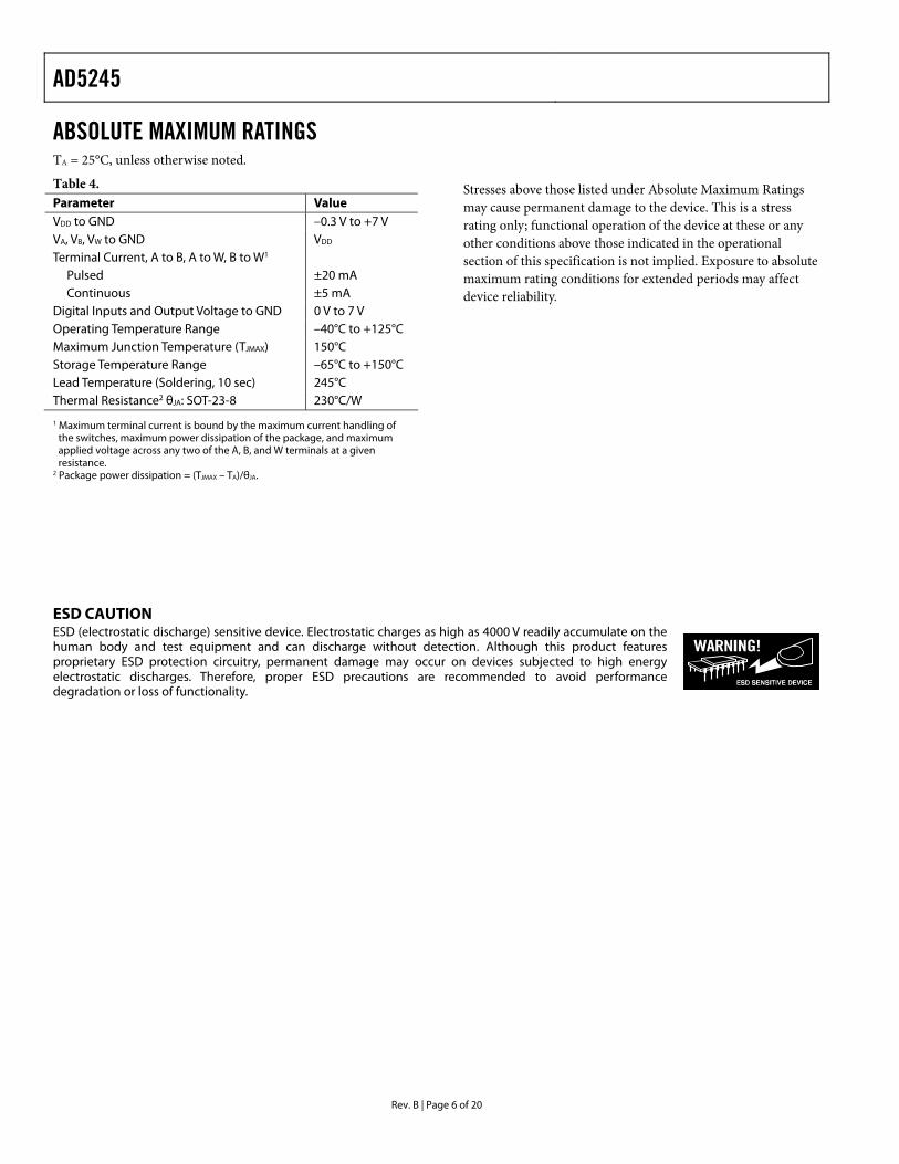
ABSOLUTE MAXIMUM RATINGS TA = 25°C, unless otherwise noted.
Table 4. Parameter Value VDD to GND –0.3 V to +7 V VA, VB, VW to GND VDD
Terminal Current, A to B, A to W, B to W1 Pulsed ±20 mA Continuous ±5 mA
Digital Inputs and Output Voltage to GND 0 V to 7 V Operating Temperature Range –40°C to +125°C Maximum Junction Temperature (TJMAX) 150°C Storage Temperature Range –65°C to +150°C Lead Temperature (Soldering, 10 sec) 245°C Thermal Resistance2 θJA: SOT-23-8 230°C/W
1 Maximum terminal current is bound by the maximum current handling of the switches, maximum power dissipation of the package, and maximum applied voltage across any two of the A, B, and W terminals at a given resistance.
2 Package power dissipation = (TJMAX – TA)/θJA.
Stresses above those listed under Absolute Maximum Ratings may cause permanent damage to the device. This is a stress rating only; functional operation of the device at these or any other conditions above those indicated in the operational section of this specification is not implied. Exposure to absolute maximum rating conditions for extended periods may affect device reliability.
ESD CAUTION ESD (electrostatic discharge) sensitive device. Electrostatic charges as high as 4000 V readily accumulate on the human body and test equipment and can discharge without detection. Although this product features proprietary ESD protection circuitry, permanent damage may occur on devices subjected to high energy electrostatic discharges. Therefore, proper ESD precautions are recommended to avoid performance degradation or loss of functionality.
AD5245
Rev. B | Page 7 of 20
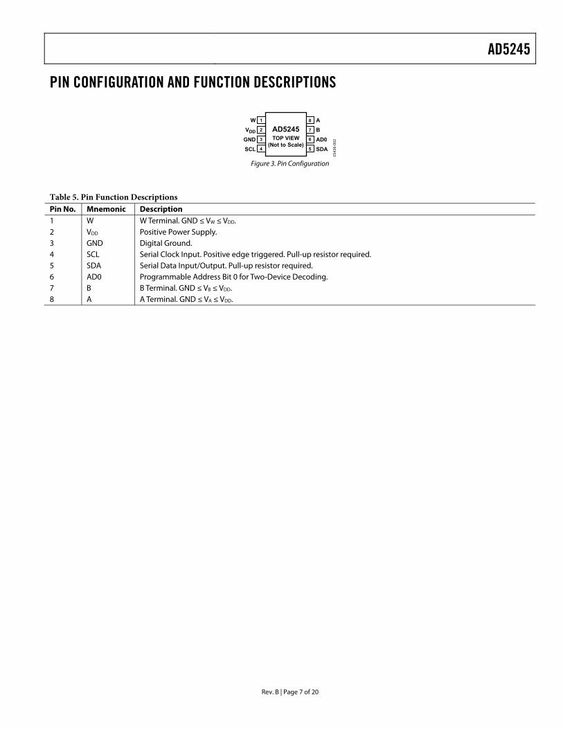
PIN CONFIGURATION AND FUNCTION DESCRIPTIONS
A
B
AD0
SDA
1
2
3
4 5
8
7
6
W
VDD
GND
SCL
AD5245TOP VIEW
(Not to Scale)
0343
6-00
2
Figure 3. Pin Configuration
Table 5. Pin Function Descriptions Pin No. Mnemonic Description 1 W W Terminal. GND ≤ VW ≤ VDD. 2 VDD Positive Power Supply. 3 GND Digital Ground. 4 SCL Serial Clock Input. Positive edge triggered. Pull-up resistor required. 5 SDA Serial Data Input/Output. Pull-up resistor required. 6 AD0 Programmable Address Bit 0 for Two-Device Decoding. 7 B B Terminal. GND ≤ VB ≤ VDD. 8 A A Terminal. GND ≤ VA ≤ VDD.
AD5245
Rev. B | Page 8 of 20
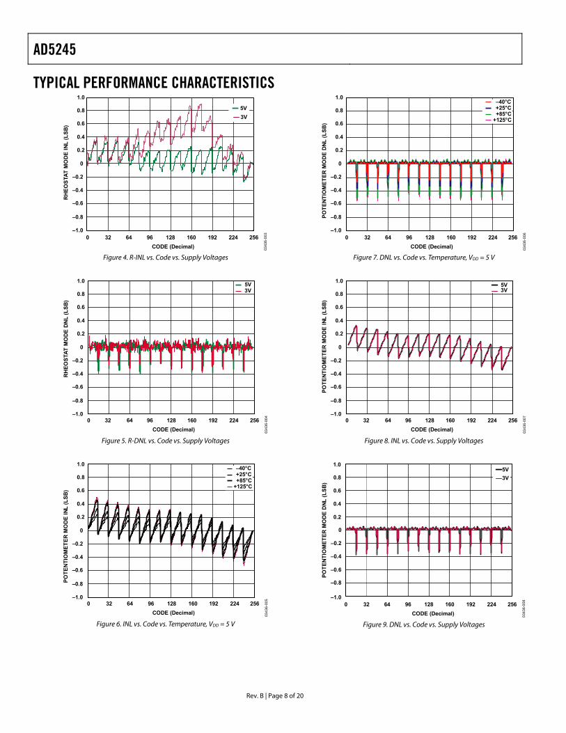
TYPICAL PERFORMANCE CHARACTERISTICS
CODE (Decimal)
–1.0
–0.8
–0.6
–0.4
–0.2
0
0.2
0.4
0.6
1.0
320 9664 128 160 192 224 256
RH
EOST
AT M
OD
E IN
L (L
SB)
0.8 5V3V
0343
6-00
3
Figure 4. R-INL vs. Code vs. Supply Voltages
5V3V
–1.0
–0.8
–0.6
–0.4
–0.2
0
0.2
0.4
0.6
1.0
RH
EOST
AT M
OD
E D
NL
(LSB
)
0.8
CODE (Decimal)320 9664 128 160 192 224 256
0343
6-00
4
Figure 5. R-DNL vs. Code vs. Supply Voltages
–40°C+25°C+85°C
+125°C
–1.0
–0.8
–0.6
–0.4
–0.2
0
0.2
0.4
0.6
1.0
POTE
NTI
OM
ETER
MO
DE
INL
(LSB
)
0.8
CODE (Decimal)320 9664 128 160 192 224 256
0343
6-00
5
Figure 6. INL vs. Code vs. Temperature, VDD = 5 V
CODE (Decimal)
–1.0
–0.8
–0.6
–0.4
–0.2
0
0.2
0.4
0.6
1.0
320 9664 128 160 192 224 256
POTE
NTI
OM
ETER
MO
DE
DNL
(LSB
)
0.8–40°C+25°C+85°C
+125°C
0343
6-00
6
Figure 7. DNL vs. Code vs. Temperature, VDD = 5 V
–1.0
–0.8
–0.6
–0.4
–0.2
0
0.2
0.4
0.6
1.0
POTE
NTI
OM
ETER
MO
DE
INL
(LSB
)
0.8
CODE (Decimal)320 9664 128 160 192 224 256
5V3V
0343
6-00
7
Figure 8. INL vs. Code vs. Supply Voltages
5V3V
CODE (Decimal)
–1.0
–0.8
–0.6
–0.4
–0.2
0
0.2
0.4
0.6
0.8
320 9664 128 160 192 224 256
POTE
NTI
OM
ETER
MO
DE
DNL
(LSB
)
1.0
0343
6-00
8
Figure 9. DNL vs. Code vs. Supply Voltages
AD5245
Rev. B | Page 9 of 20
–1.0
–0.8
–0.6
–0.4
–0.2
0
0.2
0.4
0.6
1.0R
HEO
STAT
MO
DE
INL
(LSB
)0.8
CODE (Decimal)320 9664 128 160 192 224 256
°C+25°C+85°C
+125°C
–40
0343
6-00
9
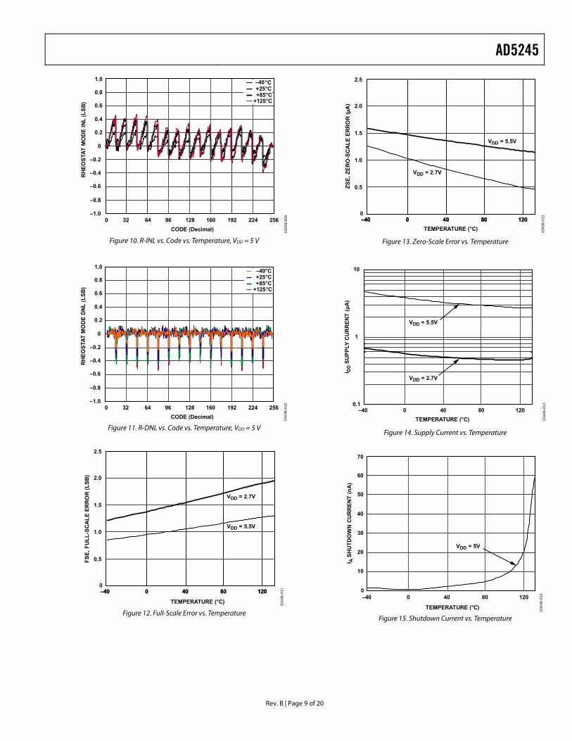
Figure 10. R-INL vs. Code vs. Temperature, VDD = 5 V
–1.0
–0.8
–0.6
–0.4
–0.2
0
0.2
0.4
0.6
1.0
RH
EOST
AT M
OD
E D
NL (L
SB)
0.8
CODE (Decimal)320 9664 128 160 192 224 256
–40°C+25°C+85°C
+125°C03
436-
010
Figure 11. R-DNL vs. Code vs. Temperature, VDD = 5 V
TEMPERATURE (°C)
0 40 80 120–400
1.5
FSE,
FU
LL-S
CA
LE E
RR
OR
(LSB
)
0 40 80 120–40
1.0
2.5
VDD = 5.5V
VDD = 2.7V
2.0
0.5
0343
6-01
1
Figure 12. Full-Scale Error vs. Temperature
0 40 80 120–400
1.5
ZSE,
ZER
O-S
CA
LE E
RR
OR
(µA
)
TEMPERATURE (°C)0 40 80 120–40
1.0
2.5
VDD = 5.5V
VDD = 2.7V
2.0
0.5
0343
6-01
2
Figure 13. Zero-Scale Error vs. Temperature
TEMPERATURE (°C)0 40 80 120–40
0.1
1
10
I DD
SUPP
LY C
UR
REN
T (µ
A)
VDD = 5.5V
VDD = 2.7V
0343
6-01
3
Figure 14. Supply Current vs. Temperature
I ASH
UTD
OW
N C
UR
REN
T (n
A)
TEMPERATURE (°C)
00
70
20
10
30
40
50
60
40 80 120–40
VDD = 5V03
436-
014
Figure 15. Shutdown Current vs. Temperature
AD5245
Rev. B | Page 10 of 20
CODE (Decimal)
–50
0
50
100
150
200
320 9664 128 160 192 224 256
RH
EOST
AT M
OD
E TE
MPC
O (p
pm/°C
)
0343
6-01
5
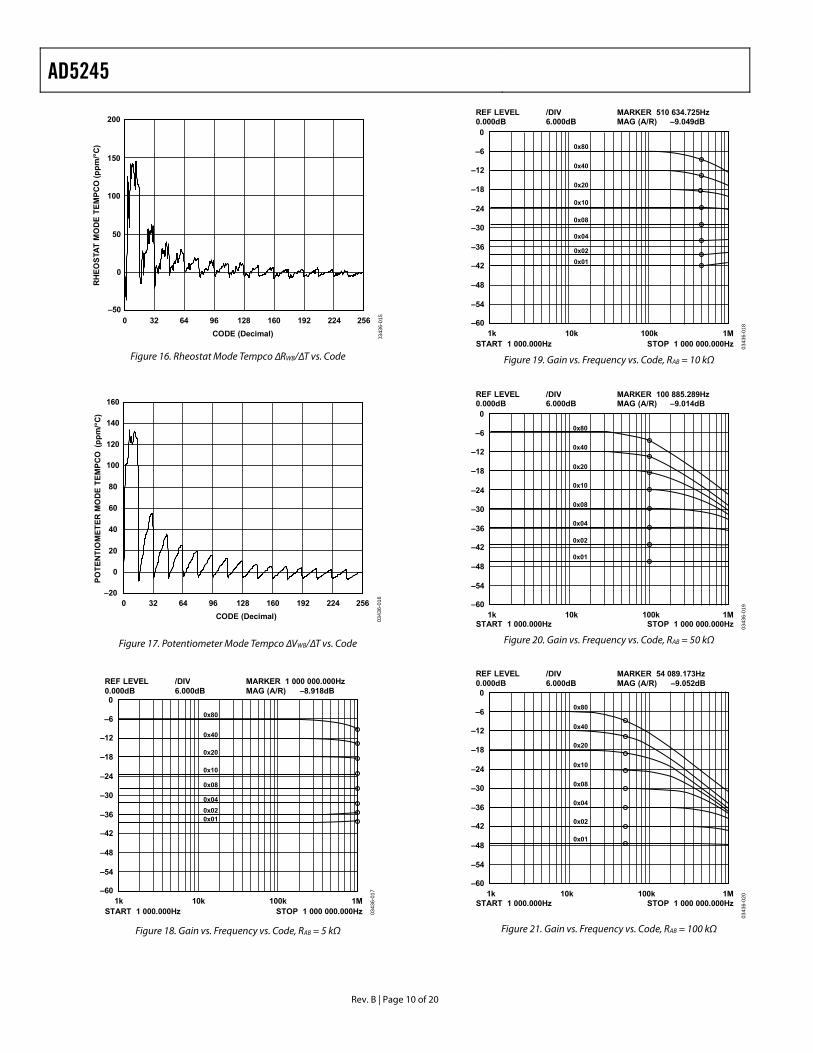
Figure 16. Rheostat Mode Tempco ∆RWB/∆T vs. Code
CODE (Decimal)
–20
0
20
40
60
80
100
120
140
160
320 9664 128 160 192 224 256
POTE
NTI
OM
ETER
MO
DE
TEM
PCO
(ppm
/°C)
0343
6-01
6
Figure 17. Potentiometer Mode Tempco ∆VWB/∆T vs. Code
1k 10k 100k 1M
0
–6
–12
–18
–24
–30
–36
–42
–48
–54
–60
0x80
0x40
0x20
0x10
0x08
0x040x020x01
REF LEVEL0.000dB
/DIV6.000dB
MARKER 1 000 000.000HzMAG (A/R) –8.918dB
START 1 000.000Hz STOP 1 000 000.000Hz 0343
6-01
7
Figure 18. Gain vs. Frequency vs. Code, RAB = 5 kΩ
1k 10k 100k 1M
0
–6
–12
–18
–24
–30
–36
–42
–48
–54
–60
0x80
0x40
0x20
0x10
0x08
0x04
0x020x01
REF LEVEL0.000dB
/DIV6.000dB
MARKER 510 634.725HzMAG (A/R) –9.049dB
START 1 000.000Hz STOP 1 000 000.000Hz 0343
6-01
8
Figure 19. Gain vs. Frequency vs. Code, RAB = 10 kΩ
1k 10k 100k 1M
0
–6
–12
–18
–24
–30
–36
–42
–48
–54
–60
0x80
0x40
0x20
0x10
0x08
0x04
0x02
0x01
REF LEVEL0.000dB
/DIV6.000dB
MARKER 100 885.289HzMAG (A/R) –9.014dB
START 1 000.000Hz STOP 1 000 000.000Hz 0343
6-01
9
Figure 20. Gain vs. Frequency vs. Code, RAB = 50 kΩ
1k 10k 100k 1M
0
–6
–12
–18
–24
–30
–36
–42
–48
–54
–60
0x80
0x40
0x20
0x10
0x08
0x04
0x02
0x01
REF LEVEL0.000dB
/DIV6.000dB
MARKER 54 089.173HzMAG (A/R) –9.052dB
START 1 000.000Hz STOP 1 000 000.000Hz
0343
6-02
0
Figure 21. Gain vs. Frequency vs. Code, RAB = 100 kΩ
AD5245
Rev. B | Page 11 of 20
10k 100k 1M 10M
–5.5
–6.0
–6.5
–7.0
–7.5
–8.0
–8.5
–9.0
–9.5
–10.0
–10.5
REF LEVEL–5.000dB
/DIV0.500dB
START 1 000.000Hz STOP 1 000 000.000Hz
R = 5kΩ
R = 10kΩ
R = 50kΩ
R = 100kΩ
5kΩ – 1.026MHz10kΩ – 511kHz50kΩ – 101kHz100kΩ – 54kHz
0343
6-02
1
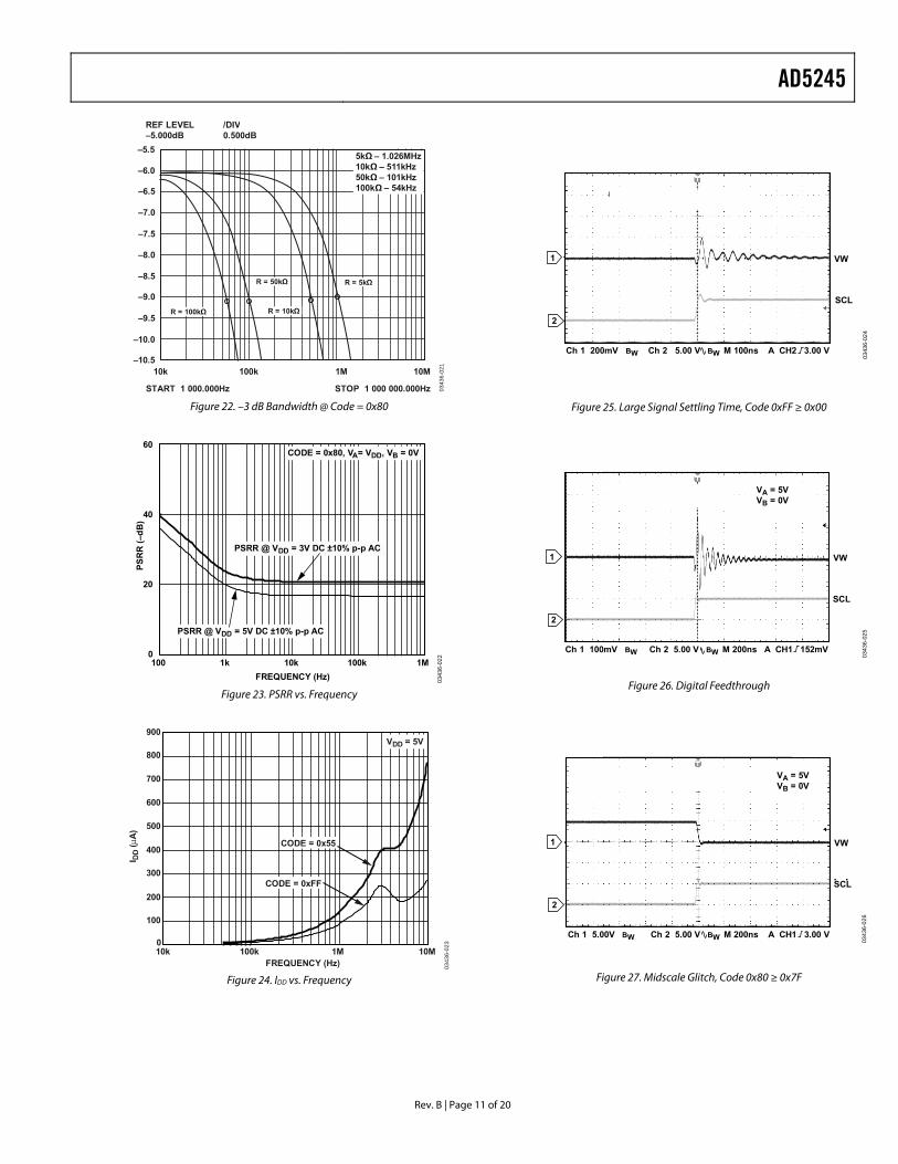
Figure 22. –3 dB Bandwidth @ Code = 0x80
FREQUENCY (Hz)10k100 100k 1M1k
0
20
40
60
PSR
R (–
dB)
CODE = 0x80, VA= VDD, VB = 0V
PSRR @ VDD = 3V DC ±10% p-p AC
0343
6-02
2
PSRR @ VDD = 5V DC ±10% p-p AC
Figure 23. PSRR vs. Frequency
I DD
(µA
)
FREQUENCY (Hz)10k
800
700
600
500
400
300
900
200
100
100k 1M 10M0
CODE = 0x55
CODE = 0xFF
VDD = 5V
0343
6-02
3
Figure 24. IDD vs. Frequency
VW
SCL
Ch 1 200mV BW Ch 2 5.00 V BW M 100ns A CH2 3.00 V
1
2
0343
6-02
4
Figure 25. Large Signal Settling Time, Code 0xFF ≥ 0x00
VW
SCL
Ch 1 100mV BW Ch 2 5.00 V BW M 200ns A CH1 152mV
1
2
VA = 5VVB = 0V
0343
6-02
5
Figure 26. Digital Feedthrough
VW
SCL
Ch 1 5.00V BW Ch 2 5.00 V BW M 200ns A CH1 3.00 V
1
2
VA = 5VVB = 0V
0343
6-02
6
Figure 27. Midscale Glitch, Code 0x80 ≥ 0x7F
AD5245
Rev. B | Page 12 of 20
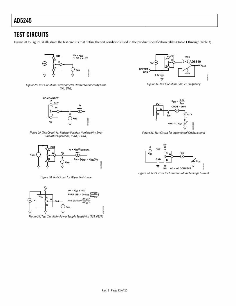
TEST CIRCUITS Figure 28 to Figure 34 illustrate the test circuits that define the test conditions used in the product specification tables (Table 1 through Table 3).
VMS
AW
B
DUT
V+
V+ = VDD1LSB = V+/2N
0343
6-02
7
Figure 28. Test Circuit for Potentiometer Divider Nonlinearity Error (INL, DNL)
NO CONNECT
IW
VMS
A W
B
DUT
0343
6-02
8
Figure 29. Test Circuit for Resistor Position Nonlinearity Error (Rheostat Operation; R-INL, R-DNL)
VMS2
VMS1
VWA
W
B
DUTIW = VDD/RNOMINAL
RW = [VMS1 – VMS2]/IW
0343
6-02
9
Figure 30. Test Circuit for Wiper Resistance
∆VMS%
DD%PSS (%/%) =
V+ = VDD ±10%
PSRR (dB) = 20 log MS
DD( )VDD
VA
VMS
AW
B
V+∆V
∆V∆V
0343
6-03
0
Figure 31. Test Circuit for Power Supply Sensitivity (PSS, PSSR)
+15V
–15V
WA
2.5V
B VOUTOFFSET
GND
DUT
AD8610VIN
0343
6-03
1
Figure 32. Test Circuit for Gain vs. Frequency
W
B
GND TO VDD
DUT
ISW
CODE = 0x00
RSW = 0.1VISW
0.1V
0343
6-03
2
Figure 33. Test Circuit for Incremental On Resistance
W
B VCM
ICMA
NC
GND
NC
VDD
DUT
NC = NO CONNECT 0343
6-03
3
Figure 34. Test Circuit for Common-Mode Leakage Current
AD5245
Rev. B | Page 13 of 20
THEORY OF OPERATION The AD5245 is a 256-position digitally controlled variable resistor (VR) device.
An internal power-on preset places the wiper at midscale during power-on, which simplifies the fault condition recovery at power-up.
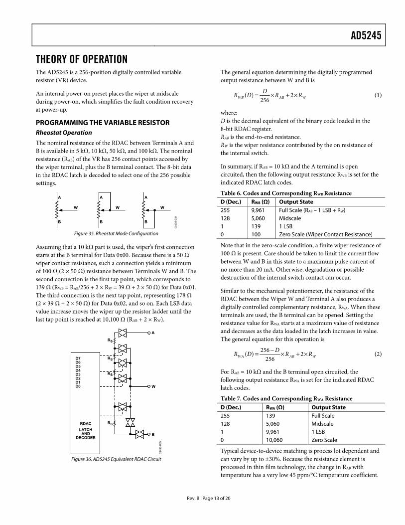
PROGRAMMING THE VARIABLE RESISTOR Rheostat Operation
The nominal resistance of the RDAC between Terminals A and B is available in 5 kΩ, 10 kΩ, 50 kΩ, and 100 kΩ. The nominal resistance (RAB) of the VR has 256 contact points accessed by the wiper terminal, plus the B terminal contact. The 8-bit data in the RDAC latch is decoded to select one of the 256 possible settings.
A
W
B
A
W
B
A
W
B
0343
6-03
4
Figure 35. Rheostat Mode Configuration
Assuming that a 10 kΩ part is used, the wiper’s first connection starts at the B terminal for Data 0x00. Because there is a 50 Ω wiper contact resistance, such a connection yields a minimum of 100 Ω (2 × 50 Ω) resistance between Terminals W and B. The second connection is the first tap point, which corresponds to 139 Ω (RWB = RAB/256 + 2 × RW = 39 Ω + 2 × 50 Ω) for Data 0x01. The third connection is the next tap point, representing 178 Ω (2 × 39 Ω + 2 × 50 Ω) for Data 0x02, and so on. Each LSB data value increase moves the wiper up the resistor ladder until the last tap point is reached at 10,100 Ω (RAB + 2 × RW).
D5D4D3
D7D6
D2D1D0
RDACLATCH
ANDDECODER
RS
RS
RS
RS
A
W
B
0343
6-03
5
Figure 36. AD5245 Equivalent RDAC Circuit
The general equation determining the digitally programmed output resistance between W and B is
WABWB RRDDR ×+×= 2256
)( (1)
where: D is the decimal equivalent of the binary code loaded in the 8-bit RDAC register. RAB is the end-to-end resistance. RW is the wiper resistance contributed by the on resistance of the internal switch.
In summary, if RAB = 10 kΩ and the A terminal is open circuited, then the following output resistance RWB is set for the indicated RDAC latch codes.
Table 6. Codes and Corresponding RWB Resistance D (Dec.) RWB (Ω) Output State 255 9,961 Full Scale (RAB – 1 LSB + RW) 128 5,060 Midscale 1 139 1 LSB 0 100 Zero Scale (Wiper Contact Resistance)
Note that in the zero-scale condition, a finite wiper resistance of 100 Ω is present. Care should be taken to limit the current flow between W and B in this state to a maximum pulse current of no more than 20 mA. Otherwise, degradation or possible destruction of the internal switch contact can occur.
Similar to the mechanical potentiometer, the resistance of the RDAC between the Wiper W and Terminal A also produces a digitally controlled complementary resistance, RWA. When these terminals are used, the B terminal can be opened. Setting the resistance value for RWA starts at a maximum value of resistance and decreases as the data loaded in the latch increases in value. The general equation for this operation is
WABWA RRDDR ×+×−= 2256
256)( (2)
For RAB = 10 kΩ and the B terminal open circuited, the following output resistance RWA is set for the indicated RDAC latch codes.
Table 7. Codes and Corresponding RWA Resistance D (Dec.) RWA (Ω) Output State 255 139 Full Scale 128 5,060 Midscale 1 9,961 1 LSB 0 10,060 Zero Scale
Typical device-to-device matching is process lot dependent and can vary by up to ±30%. Because the resistance element is processed in thin film technology, the change in RAB with temperature has a very low 45 ppm/°C temperature coefficient.
AD5245
Rev. B | Page 14 of 20
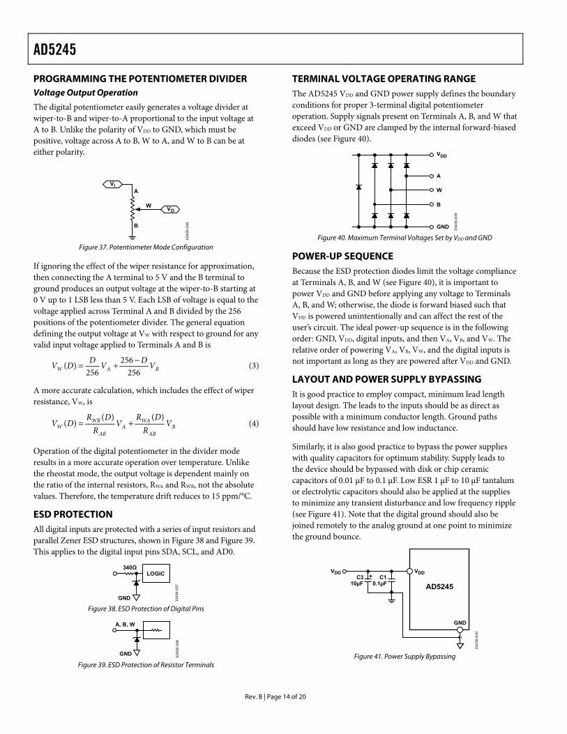
PROGRAMMING THE POTENTIOMETER DIVIDER Voltage Output Operation
The digital potentiometer easily generates a voltage divider at wiper-to-B and wiper-to-A proportional to the input voltage at A to B. Unlike the polarity of VDD to GND, which must be positive, voltage across A to B, W to A, and W to B can be at either polarity.
AVI
W
B
VO
0343
6-03
6
Figure 37. Potentiometer Mode Configuration
If ignoring the effect of the wiper resistance for approximation, then connecting the A terminal to 5 V and the B terminal to ground produces an output voltage at the wiper-to-B starting at 0 V up to 1 LSB less than 5 V. Each LSB of voltage is equal to the voltage applied across Terminal A and B divided by the 256 positions of the potentiometer divider. The general equation defining the output voltage at VW with respect to ground for any valid input voltage applied to Terminals A and B is
BAW VDVDDV256
256256
)( −+= (3)
A more accurate calculation, which includes the effect of wiper resistance, VW, is
BAB
WAA
AB
WBW V
RDR
VR
DRDV
)()()( += (4)
Operation of the digital potentiometer in the divider mode results in a more accurate operation over temperature. Unlike the rheostat mode, the output voltage is dependent mainly on the ratio of the internal resistors, RWA and RWB, not the absolute values. Therefore, the temperature drift reduces to 15 ppm/°C.
ESD PROTECTION All digital inputs are protected with a series of input resistors and parallel Zener ESD structures, shown in Figure 38 and Figure 39. This applies to the digital input pins SDA, SCL, and AD0.
LOGIC340Ω
GND 0343
6-03
7
Figure 38. ESD Protection of Digital Pins
A, B, W
GND 0343
6-03
8
Figure 39. ESD Protection of Resistor Terminals
TERMINAL VOLTAGE OPERATING RANGE The AD5245 VDD and GND power supply defines the boundary conditions for proper 3-terminal digital potentiometer operation. Supply signals present on Terminals A, B, and W that exceed VDD or GND are clamped by the internal forward-biased diodes (see Figure 40).
GND
A
W
B
VDD
0343
6-03
9
Figure 40. Maximum Terminal Voltages Set by VDD and GND
POWER-UP SEQUENCE Because the ESD protection diodes limit the voltage compliance at Terminals A, B, and W (see Figure 40), it is important to power VDD and GND before applying any voltage to Terminals A, B, and W; otherwise, the diode is forward biased such that VDD is powered unintentionally and can affect the rest of the user’s circuit. The ideal power-up sequence is in the following order: GND, VDD, digital inputs, and then VA, VB, and VW. The relative order of powering VA, VB, VW, and the digital inputs is not important as long as they are powered after VDD and GND.
LAYOUT AND POWER SUPPLY BYPASSING It is good practice to employ compact, minimum lead length layout design. The leads to the inputs should be as direct as possible with a minimum conductor length. Ground paths should have low resistance and low inductance.
Similarly, it is also good practice to bypass the power supplies with quality capacitors for optimum stability. Supply leads to the device should be bypassed with disk or chip ceramic capacitors of 0.01 µF to 0.1 µF. Low ESR 1 µF to 10 µF tantalum or electrolytic capacitors should also be applied at the supplies to minimize any transient disturbance and low frequency ripple (see Figure 41). Note that the digital ground should also be joined remotely to the analog ground at one point to minimize the ground bounce.
VDD
GND
VDDC3
10µFC1
0.1µF AD5245+
0343
6-04
0
Figure 41. Power Supply Bypassing
AD5245
Rev. B | Page 15 of 20
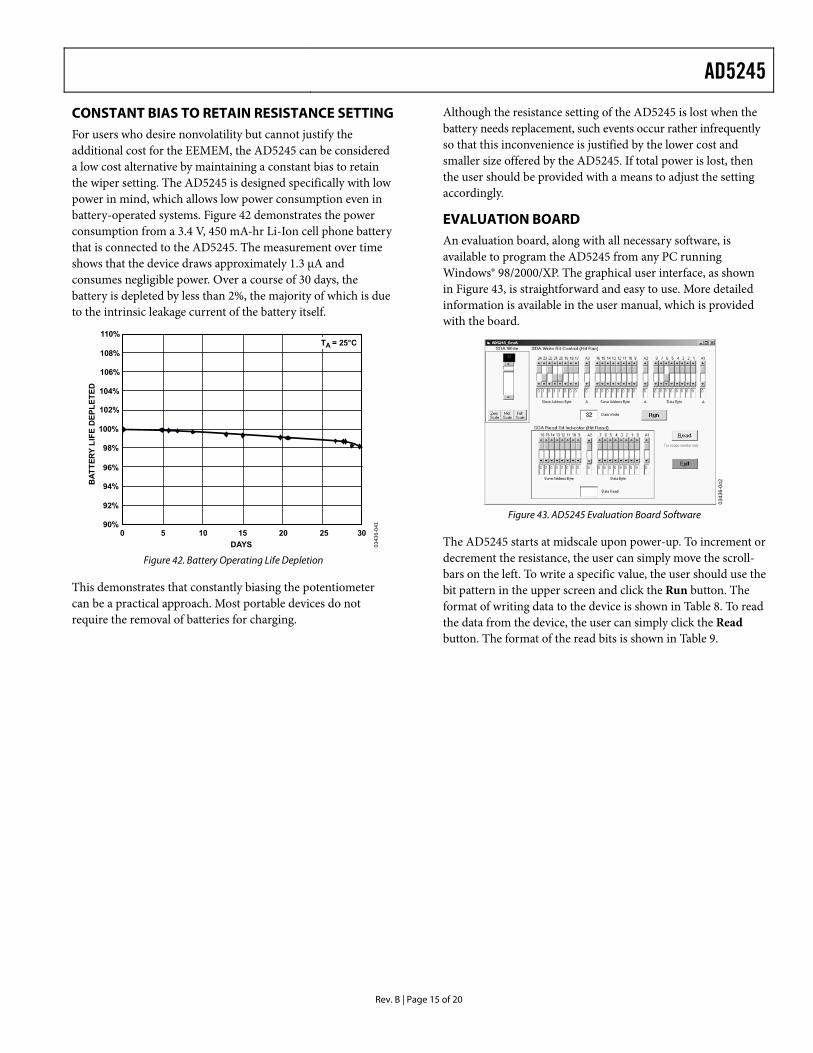
CONSTANT BIAS TO RETAIN RESISTANCE SETTING For users who desire nonvolatility but cannot justify the additional cost for the EEMEM, the AD5245 can be considered a low cost alternative by maintaining a constant bias to retain the wiper setting. The AD5245 is designed specifically with low power in mind, which allows low power consumption even in battery-operated systems. Figure 42 demonstrates the power consumption from a 3.4 V, 450 mA-hr Li-Ion cell phone battery that is connected to the AD5245. The measurement over time shows that the device draws approximately 1.3 µA and consumes negligible power. Over a course of 30 days, the battery is depleted by less than 2%, the majority of which is due to the intrinsic leakage current of the battery itself.
DAYS
BAT
TERY
LIF
E D
EPLE
TED
090%
92%
94%
96%
5 10 15
98%
100%
102%
104%
106%
108%
110%
20 25 30
TA = 25°C
0343
6-04
1
Figure 42. Battery Operating Life Depletion
This demonstrates that constantly biasing the potentiometer can be a practical approach. Most portable devices do not require the removal of batteries for charging.
Although the resistance setting of the AD5245 is lost when the battery needs replacement, such events occur rather infrequently so that this inconvenience is justified by the lower cost and smaller size offered by the AD5245. If total power is lost, then the user should be provided with a means to adjust the setting accordingly.
EVALUATION BOARD An evaluation board, along with all necessary software, is available to program the AD5245 from any PC running Windows® 98/2000/XP. The graphical user interface, as shown in Figure 43, is straightforward and easy to use. More detailed information is available in the user manual, which is provided with the board.
0343
6-04
2
Figure 43. AD5245 Evaluation Board Software
The AD5245 starts at midscale upon power-up. To increment or decrement the resistance, the user can simply move the scroll-bars on the left. To write a specific value, the user should use the bit pattern in the upper screen and click the Run button. The format of writing data to the device is shown in Table 8. To read the data from the device, the user can simply click the Read button. The format of the read bits is shown in Table 9.
AD5245
Rev. B | Page 16 of 20
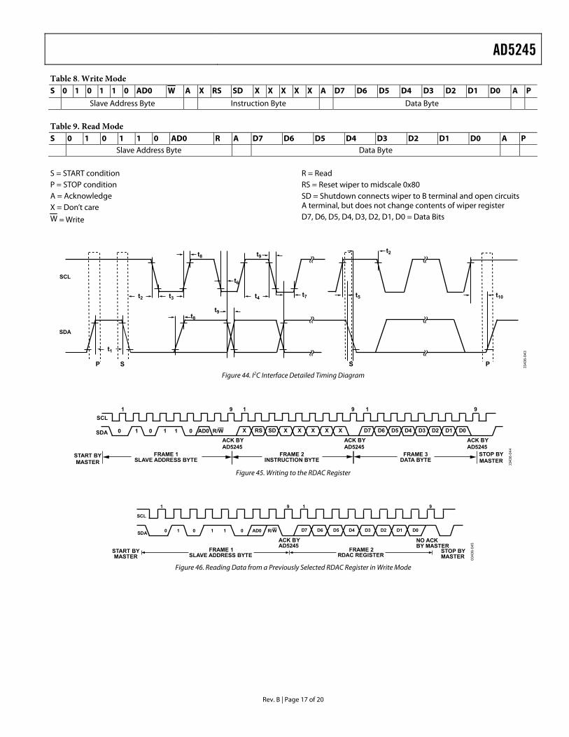
I2C INTERFACE I2C-COMPATIBLE 2-WIRE SERIAL BUS The 2-wire I2C serial bus protocol operates as follows:
1. The master initiates data transfer by establishing a START condition, which is when a high-to-low transition on the SDA line occurs while SCL is high (see Figure 45). The next byte is the slave address byte, which consists of the 7-bit slave address followed by an R/W bit (this bit determines whether data is read from or written to the slave device). The AD5245 has one configurable address bit, AD0 (see Table 8). The slave whose address corresponds to the transmitted address responds by pulling the SDA line low during the ninth clock pulse (this is termed the acknowledge bit). At this stage, all other devices on the bus remain idle while the selected device waits for data to be written to or read from its serial register. If the R/W bit is high, the master reads from the slave device. On the other hand, if the R/W bit is low, the master writes to the slave device.
2. In write mode, the second byte is the instruction byte. The first bit (MSB) of the instruction byte is a don’t care. The second MSB, RS, is the midscale reset. A logic high on this bit moves the wiper to the center tap, where RWA = RWB. This feature effectively overwrites the contents of the register; therefore, when taken out of reset mode, the RDAC remains at midscale. The third MSB, SD, is a shutdown bit. A logic high causes an open circuit at Terminal A while shorting the wiper to Terminal B. This operation yields almost 0 Ω in rheostat mode or 0 V in potentiometer mode. It is important to note that the shutdown operation does not disturb the contents of the register. When brought out of shutdown, the previous setting is applied to the RDAC. Also during shutdown, new settings can be programmed. When the part is returned from shutdown, the corresponding VR setting is applied to the RDAC. The remainder of the bits in the instruction byte are don’t cares (see Table 8).
3. After acknowledging the instruction byte, the last byte in write mode is the data byte. Data is transmitted over the serial bus in sequences of nine clock pulses (eight data bits followed by an acknowledge bit). The transitions on the SDA line must occur during the low period of SCL and remain stable during the high period of SCL (see Figure 45).
4. In read mode, the data byte follows immediately after the acknowledgment of the slave address byte. Data is transmitted over the serial bus in sequences of nine clock pulses (a slight difference with write mode, in which eight data bits are followed by an acknowledge bit). Similarly, the transitions on the SDA line must occur during the low period of SCL and remain stable during the high period of SCL (see Figure 46).
5. After all data bits have been read or written, a STOP condition is established by the master. A STOP condition is defined as a low-to-high transition on the SDA line while SCL is high. In write mode, the master pulls the SDA line high during the 10th clock pulse to establish a STOP condition (see Figure 45). In read mode, the master issues a no acknowledge for the ninth clock pulse (that is, the SDA line remains high). The master then brings the SDA line low before the 10th clock pulse, which goes high to establish a STOP condition (see Figure 46). A repeated write function gives the user flexibility to update the RDAC output a number of times after addressing and instructing the part only once. For example, after the RDAC has acknowledged its slave address and instruction bytes in the write mode, the RDAC output updates on each successive byte. If different instructions are needed, then the write/read mode has to start again with a new slave address, instruction, and data byte. Similarly, a repeated read function of the RDAC is also allowed.
AD5245
Rev. B | Page 17 of 20
Table 8. Write Mode S 0 1 0 1 1 0 AD0 W A X RS SD X X X X X A D7 D6 D5 D4 D3 D2 D1 D0 A P
Slave Address Byte Instruction Byte Data Byte Table 9. Read Mode S 0 1 0 1 1 0 AD0 R A D7 D6 D5 D4 D3 D2 D1 D0 A P
Slave Address Byte Data Byte S = START condition P = STOP condition A = Acknowledge X = Don’t care W = Write
R = Read RS = Reset wiper to midscale 0x80 SD = Shutdown connects wiper to B terminal and open circuits A terminal, but does not change contents of wiper register D7, D6, D5, D4, D3, D2, D1, D0 = Data Bits
t1
t3 t4t2 t7
t8t9
P S PS
t10t5
t9t8
SCL
SDA
t2
t6
0343
6-04
3
Figure 44. I2C Interface Detailed Timing Diagram
SCL
FRAME 1 FRAME 2START BYMASTER
ACK BYAD5245
SLAVE ADDRESS BYTESTOP BYMASTERINSTRUCTION BYTE
SDA 0 1 0 1 1 0 AD0 R/W X RS X X X X X
1 91 9
D7 D6 D5 D4 D3 D2 D1 D0
ACK BYAD5245
FRAME 3DATA BYTE
19
ACK BYAD5245
SD
0343
6-04
4
Figure 45. Writing to the RDAC Register
NO ACKBY MASTER
SCL
SDA 0 1 0 1 1 0 AD0 R/W D7 D6 D5 D4 D3 D2 D1 D0
1 919
FRAME 1 FRAME 2START BYMASTER
ACK BYAD5245
SLAVE ADDRESS BYTE RDAC REGISTERSTOP BYMASTER 03
436-
045
Figure 46. Reading Data from a Previously Selected RDAC Register in Write Mode
AD5245
Rev. B | Page 18 of 20
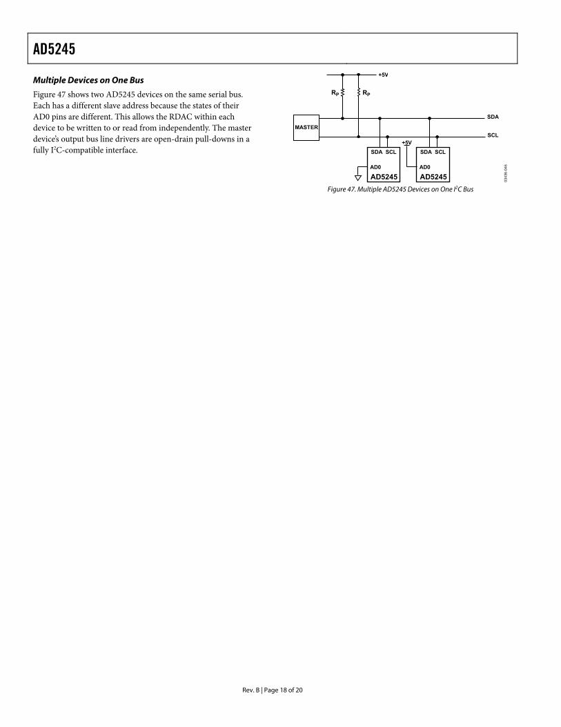
Multiple Devices on One Bus
Figure 47 shows two AD5245 devices on the same serial bus. Each has a different slave address because the states of their AD0 pins are different. This allows the RDAC within each device to be written to or read from independently. The master device’s output bus line drivers are open-drain pull-downs in a fully I2C-compatible interface.
MASTER
AD5245
SDA SCL
RP RP
+5V
+5V
SDA
SCL
SDA SCL
AD5245AD0 AD0
0343
6-04
6
Figure 47. Multiple AD5245 Devices on One I2C Bus
AD5245
Rev. B | Page 19 of 20
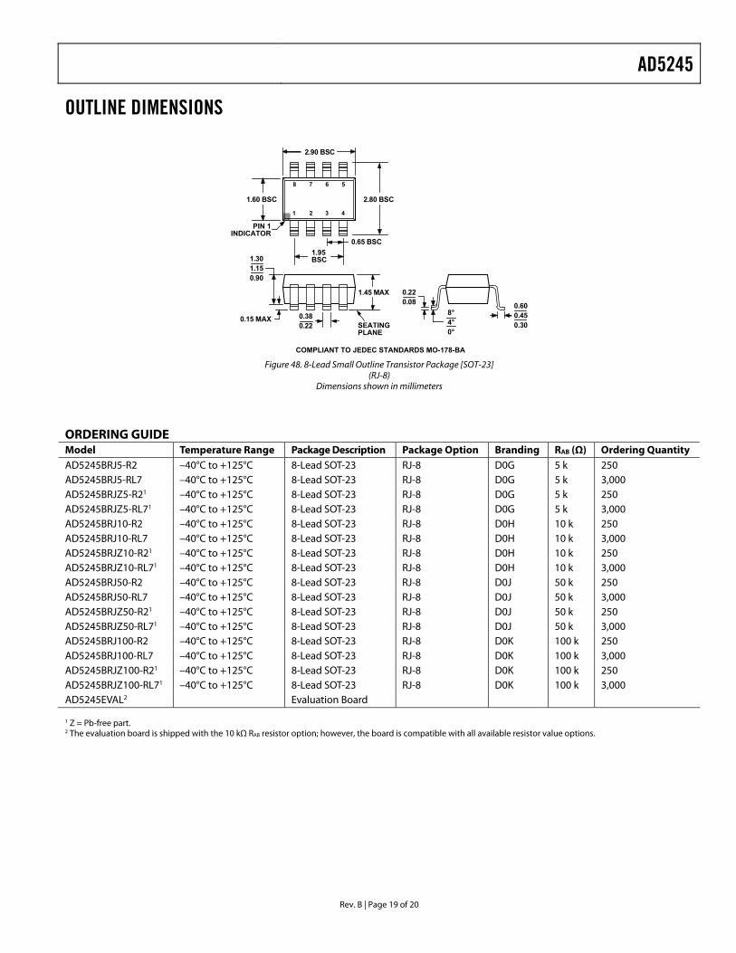
OUTLINE DIMENSIONS
1 3
56
2
8
4
7
2.90 BSC
1.60 BSC
1.95BSC
0.65 BSC
0.380.22
0.15 MAX
1.301.150.90
SEATINGPLANE
1.45 MAX 0.220.08 0.60
0.450.30
8°4°0°
2.80 BSC
PIN 1INDICATOR
COMPLIANT TO JEDEC STANDARDS MO-178-BA Figure 48. 8-Lead Small Outline Transistor Package [SOT-23]
(RJ-8) Dimensions shown in millimeters
ORDERING GUIDE Model Temperature Range Package Description Package Option Branding RAB (Ω) Ordering Quantity AD5245BRJ5-R2 –40°C to +125°C 8-Lead SOT-23 RJ-8 D0G 5 k 250 AD5245BRJ5-RL7 –40°C to +125°C 8-Lead SOT-23 RJ-8 D0G 5 k 3,000 AD5245BRJZ5-R21 –40°C to +125°C 8-Lead SOT-23 RJ-8 D0G 5 k 250 AD5245BRJZ5-RL71 –40°C to +125°C 8-Lead SOT-23 RJ-8 D0G 5 k 3,000 AD5245BRJ10-R2 –40°C to +125°C 8-Lead SOT-23 RJ-8 D0H 10 k 250 AD5245BRJ10-RL7 –40°C to +125°C 8-Lead SOT-23 RJ-8 D0H 10 k 3,000 AD5245BRJZ10-R21 –40°C to +125°C 8-Lead SOT-23 RJ-8 D0H 10 k 250 AD5245BRJZ10-RL71 –40°C to +125°C 8-Lead SOT-23 RJ-8 D0H 10 k 3,000 AD5245BRJ50-R2 –40°C to +125°C 8-Lead SOT-23 RJ-8 D0J 50 k 250 AD5245BRJ50-RL7 –40°C to +125°C 8-Lead SOT-23 RJ-8 D0J 50 k 3,000 AD5245BRJZ50-R21 –40°C to +125°C 8-Lead SOT-23 RJ-8 D0J 50 k 250 AD5245BRJZ50-RL71 –40°C to +125°C 8-Lead SOT-23 RJ-8 D0J 50 k 3,000 AD5245BRJ100-R2 –40°C to +125°C 8-Lead SOT-23 RJ-8 D0K 100 k 250 AD5245BRJ100-RL7 –40°C to +125°C 8-Lead SOT-23 RJ-8 D0K 100 k 3,000 AD5245BRJZ100-R21 –40°C to +125°C 8-Lead SOT-23 RJ-8 D0K 100 k 250 AD5245BRJZ100-RL71 –40°C to +125°C 8-Lead SOT-23 RJ-8 D0K 100 k 3,000 AD5245EVAL2 Evaluation Board 1 Z = Pb-free part. 2 The evaluation board is shipped with the 10 kΩ RAB resistor option; however, the board is compatible with all available resistor value options.

AD5245
Rev. B | Page 20 of 20
NOTES
Purchase of licensed I2C components of Analog Devices or one of its sublicensed Associated Companies conveys a license for the purchaser under the Philips I2C Patent Rights to use these components in an I2C system, provided that the system conforms to the I2C Standard Specification as defined by Philips.
©2006 Analog Devices, Inc. All rights reserved. Trademarks and registered trademarks are the property of their respective owners. C03436-0-1/06(B)