2656 ieee transactions on microwave … lee/2005 tmtt no 9.pdf · tapered dual-plane compact...
TRANSCRIPT

2656 IEEE TRANSACTIONS ON MICROWAVE THEORY AND TECHNIQUES, VOL. 53, NO. 9, SEPTEMBER 2005
Tapered Dual-Plane Compact ElectromagneticBandgap Microstrip Filter Structures
Shao Ying Huang, Student Member, IEEE, and Yee Hui Lee, Member, IEEE
Abstract—In this paper, the designs of two novel tapereddual-plane compact electromagnetic bandgap (C-EBG) microstripfilter structures are presented. With the dual-plane configuration,the proposed structure displays an ultrawide stopband with highattenuation within a small circuit area. Chebyshev distributionis adopted to eliminate ripples in the passband caused by theperiodicity of the EBG structure. This gives rise to a compactEBG structure that exhibits excellent transmission and rejectioncharacteristics in the passband and the stopband, respectively.The proposed structures are implemented and the measurementresults are found to be in good agreement with the simulationresults, verifying the excellent stopband and passband perfor-mance obtained using the proposed configuration. These novelstructures are easy to fabricate and are promising structuresthat have wide applications for compact and high performancecircuit component designs in microwave circuits.
Index Terms—Bandstop filters, dual-plane, electromagneticbandgap (EBG) structures, low sidelobe array theory, microstripfilters, tapering functions, tapering techniques.
I. INTRODUCTION
E LECTROMAGNETIC bandgap (EBG) structure has beena term widely accepted nowadays to name the artificial
periodic structures that prohibit the propagation of electromag-netic waves at microwave or millimeter wave frequencies. Thethree-dimensional (3-D) artificial periodic bandgap structurewas introduced at optical frequencies [1]–[3] and known asphotonic bandgap (PBG) structure. Due to the scalability of theperiodic structure, relevant research work has progressed intothe field of microwave, millimeter wave, and infrared.
The unique feature of EBG structures is the existence of thebandgap where electromagnetic waves are not allowed to prop-agate. It has been widely applied as the substrate of planar mi-crowave circuits such as patch antennas to suppress the surfacewaves [4], [5] and power amplifiers to reduce the harmonics [6].The planar EBG structure was introduced in [7] where planarperiodic elements are etched in the ground plane. It has the ad-vantage of ease of fabrication and yet capable of maintaininga similar control on the wave propagation in the structure tothat in the EBG structure with 3-D periodic elements. The onlydrawback of planar structures is that they are not able to pro-hibit the wave propagation in the entire 3-D space. Nevertheless,planar EBG structures are compatible with microstrip circuitsthus making them attractive as microstrip filters.
Manuscript received December 9, 2004; revised May 26, 2005.The authors are with the School of Electrical and Electronic Engi-
neering, Nanyang Technological University, 639798 Singapore (e-mail:[email protected]; [email protected]).
Digital Object Identifier 10.1109/TMTT.2005.854212
A microstrip line with an array of patches etched in theground plane exhibits a prominent bandgap in the transmissionalong the conducting line [7]. Due to the high confinementof electromagnetic waves around the transmission line, thewell-known one-dimensional (1-D) EBG microstrip reflectorwas proposed [8] where a single column of etched periodicelements below the line is sufficient to obtain a bandgap whenthe Bragg reflection condition is satisfied. A bandgap can beobtained in the EBG microstrip structure when the geometryof the etched patch is changed or when the periodic elementsare introduced in the microstrip line [9], [10]. Defected groundstructure (DGS) has a defect with unique geometry and is ableto exhibit an attenuation pole even with a single unit [11].
Several approaches have been taken to enhance the stopbandperformance of 1-D planar EBG microstrip Bragg reflectorswhile maintaining a reasonable ripple level in the passband andkeeping a small physical size. For example, in order to design ahigh performance bandstop filter that exhibits a wide stopbandwith high attenuation in a relatively small physical area, a me-ander 1-D EBG microstrip structure was proposed [12]. In [13],a compact EBG bandstop filter structure with a wide stopbandwas proposed by combining a 1-D periodic DGS and a modu-lated microstrip line. This structure is able to introduce an in-crease in the bandwidth of the stopband while maintaining asmall ripple level in the lower passband.
A novel tapered dual-plane compact EBG (C-EBG) mi-crostrip filter structure has been introduced in [14]. Due to thedual-plane configuration and the adopted tapering technique,the proposed structure exhibits superior passband and stopbandcharacteristics. In this paper, the characteristics of the novelunique dual-plane configuration of the proposed design arestudied in detail. A comprehensive study on the tapering tech-niques in the application for 1-D EBG microstrip structures ispresented including formulas and a comparison of the effects ofdifferent tapering techniques. In Section II, the two single-planeEBG structures that are used to construct the proposed C-EBGstructures are studied. The relative location of the single-planeEBG structures and its effects on the performance of the C-EBGstructure are examined and analyzed. A comparison betweenthe performances of the proposed structure and its associatedsingle-plane EBG structures is included. In Section III, asystematical study on tapering techniques is presented. In Sec-tion IV, two novel tapered dual-plane C-EBG microstrip filterstructures with significant elimination of ripples are proposedby adopting the Chebyshev distribution. The proposed C-EBGstructures were fabricated and tested. Experimental results arepresented in the same section.
0018-9480/$20.00 © 2005 IEEE
Authorized licensed use limited to: Nanyang Technological University. Downloaded on April 23, 2009 at 05:31 from IEEE Xplore. Restrictions apply.
HUANG AND LEE: TAPERED DUAL-PLANE COMPACT ELECTROMAGNETIC BANDGAP MICROSTRIP FILTER STRUCTURES 2657
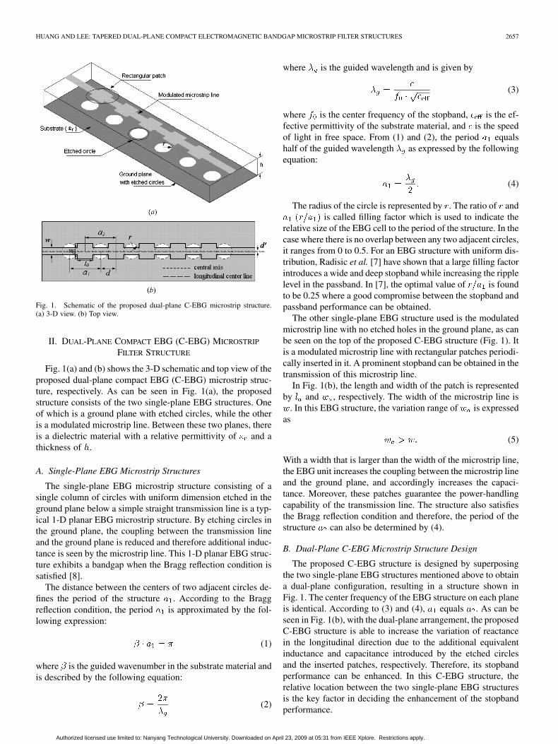
Fig. 1. Schematic of the proposed dual-plane C-EBG microstrip structure.(a) 3-D view. (b) Top view.
II. DUAL-PLANE COMPACT EBG (C-EBG) MICROSTRIP
FILTER STRUCTURE
Fig. 1(a) and (b) shows the 3-D schematic and top view of theproposed dual-plane compact EBG (C-EBG) microstrip struc-ture, respectively. As can be seen in Fig. 1(a), the proposedstructure consists of the two single-plane EBG structures. Oneof which is a ground plane with etched circles, while the otheris a modulated microstrip line. Between these two planes, thereis a dielectric material with a relative permittivity of and athickness of .
A. Single-Plane EBG Microstrip Structures
The single-plane EBG microstrip structure consisting of asingle column of circles with uniform dimension etched in theground plane below a simple straight transmission line is a typ-ical 1-D planar EBG microstrip structure. By etching circles inthe ground plane, the coupling between the transmission lineand the ground plane is reduced and therefore additional induc-tance is seen by the microstrip line. This 1-D planar EBG struc-ture exhibits a bandgap when the Bragg reflection condition issatisfied [8].
The distance between the centers of two adjacent circles de-fines the period of the structure . According to the Braggreflection condition, the period is approximated by the fol-lowing expression:
(1)
where is the guided wavenumber in the substrate material andis described by the following equation:
(2)
where is the guided wavelength and is given by
(3)
where is the center frequency of the stopband, is the ef-fective permittivity of the substrate material, and is the speedof light in free space. From (1) and (2), the period equalshalf of the guided wavelength as expressed by the followingequation:
(4)
The radius of the circle is represented by . The ratio of andis called filling factor which is used to indicate the
relative size of the EBG cell to the period of the structure. In thecase where there is no overlap between any two adjacent circles,it ranges from 0 to 0.5. For an EBG structure with uniform dis-tribution, Radisic et al. [7] have shown that a large filling factorintroduces a wide and deep stopband while increasing the ripplelevel in the passband. In [7], the optimal value of is foundto be 0.25 where a good compromise between the stopband andpassband performance can be obtained.
The other single-plane EBG structure used is the modulatedmicrostrip line with no etched holes in the ground plane, as canbe seen on the top of the proposed C-EBG structure (Fig. 1). Itis a modulated microstrip line with rectangular patches periodi-cally inserted in it. A prominent stopband can be obtained in thetransmission of this microstrip line.
In Fig. 1(b), the length and width of the patch is representedby and , respectively. The width of the microstrip line is
. In this EBG structure, the variation range of is expressedas
(5)
With a width that is larger than the width of the microstrip line,the EBG unit increases the coupling between the microstrip lineand the ground plane, and accordingly increases the capaci-tance. Moreover, these patches guarantee the power-handlingcapability of the transmission line. The structure also satisfiesthe Bragg reflection condition and therefore, the period of thestructure can also be determined by (4).
B. Dual-Plane C-EBG Microstrip Structure Design
The proposed C-EBG structure is designed by superposingthe two single-plane EBG structures mentioned above to obtaina dual-plane configuration, resulting in a structure shown inFig. 1. The center frequency of the EBG structure on each planeis identical. According to (3) and (4), equals . As can beseen in Fig. 1(b), with the dual-plane arrangement, the proposedC-EBG structure is able to increase the variation of reactancein the longitudinal direction due to the additional equivalentinductance and capacitance introduced by the etched circlesand the inserted patches, respectively. Therefore, its stopbandperformance can be enhanced. In this C-EBG structure, therelative location between the two single-plane EBG structuresis the key factor in deciding the enhancement of the stopbandperformance.
Authorized licensed use limited to: Nanyang Technological University. Downloaded on April 23, 2009 at 05:31 from IEEE Xplore. Restrictions apply.

2658 IEEE TRANSACTIONS ON MICROWAVE THEORY AND TECHNIQUES, VOL. 53, NO. 9, SEPTEMBER 2005
Fig. 2. Simulated S parameters of the dual-plane C-EBG structures with avarying d and d = 5:18 mm.
C. Effects of Relative Location Between the Two Single-PlaneEBG Structures
Due to the dual-plane configuration, the relative location ofthe single-plane EBG structure on each plane ( and ) has sig-nificant effects on the performance of the proposed structure.The transversal alignment offset and the longitudinal offsetare illustrated in Fig. 1(b). is defined as the distance betweenthe central axis of the circles and the longitudinal center line ofthe modulated microstrip line in the transversal direction. isdefined as the short distance between the centers of the adjacentetched circle and rectangular patch in the longitudinal direction.It ranges from 0 to , and periodically repeats any-where else. and indicate the relative location between thetwo single-plane EBG structures in the transversal and the lon-gitudinal direction, respectively.
The method-of-moments (MOM)-based software, ZelandIE3D is used to simulate the proposed dual-plane C-EBGmicrostrip structure (Fig. 1). The simulation model consists ofa microstrip line with five inserted square patches and a groundplane with six etched circles. The substrate used is Taconicwith a dielectric constant of 2.43 and a thickness of30 mils. To operate in the -band range, the center frequencyof each single-plane EBG structure is set to be 10 GHz. There-fore, according to the Bragg reflection condition, the period ofthe EBG structure and are both 10.35 mm. The widthof the microstrip line is set to 2.29 mm, corresponding toa characteristics impedance of 50 at 10 GHz. The fillingfactor is set to its optimal value of 0.25. Using thisoptimal filling factor, the radius of the circle is determined tobe 2.59 mm. The length and the width of the inserted patch inthe microstrip line and are both fixed to 5 mm.
Fig. 2 shows the simulated parameters of the C-EBGstructures with a fixed mm and a varying
mm mm mm . As can be seen in Fig. 2,as increases, the 10-dB stopband bandwidth reduces from7.91 to 5.70 to 3.55 GHz. The C-EBG structure with circlesetched exactly below the microstrip line ( mm) showsthe largest stopband bandwidth. The performances of thesethree C-EBG structures are tabulated in Table I. As shown inthe table, a decrease in gives rise to an increase in both thebandwidth and the attenuation within the stopband. However,
TABLE ISIMULATED PERFORMANCES OF DUAL-PLANE C-EBG STRUCTURES.
Fig. 3. Simulated S parameters of the dual-plane C-EBG structures with avarying d and d = 0 mm.
as decreases, the ripple level in both the higher and the lowerpassband increases. It is also observed that due to the higherinsertion loss at high frequencies, the ripple level in the higherpassband is always larger than that in the lower passband.
The results reveal that in the proposed dual-plane C-EBGstructure, an increase in the transversal alignment offset de-grades the stopband performance significantly with only a slightimprovement in the passband performance. This is because theequivalent inductance introduced by the etched circles dimin-ishes with an increase in due to the high confinement of fieldsaround the microstrip line. mm is the optimal locationto significantly enhance the stopband performance because itgives the largest variation of equivalent reactance in the C-EBGstructure.
Fig. 3 depicts the simulated parameters of the dual-planeC-EBG structures with a fixed mm and a varying
mm mm mm . When mm, there is nooverlap between the etched circle in the ground plane and theinserted patch in the microstrip line; when mm, theetched circle partially overlaps the inserted patch; and when
mm, they almost totally overlap each other. As can be seen inthe figure, when mm, no stopband is observed since theadditional capacitive effect introduced by the inserted squarepatches cancels the inductive effect introduced by the circlesof similar size etched in the ground plane. The performancesof the two C-EBG structures with a stopband are included inTable I. As shown in the table, when is decreased from 5.18 to2.59 mm, the stopband performance of the C-EBG structure is
Authorized licensed use limited to: Nanyang Technological University. Downloaded on April 23, 2009 at 05:31 from IEEE Xplore. Restrictions apply.

HUANG AND LEE: TAPERED DUAL-PLANE COMPACT ELECTROMAGNETIC BANDGAP MICROSTRIP FILTER STRUCTURES 2659
degraded in terms of bandwidth and attenuation. Its ripple levelin the higher passband increases while its performance in thelower passband is slightly improved.
The results obtained imply that the longitudinal offsetconsiderably affects the stopband performance of the proposeddual-plane C-EBG microstrip structure while its effect on thepassband performance is minor. The bandwidth and attenu-ation of the stopband decrease with a decreasing . This isbecause the reduction in the longitudinal offset introduces asection of microstrip line without the inductive effect, and anoverlap between the etched circle and the inserted patch wherethe inductive effect introduced by the etched circle cancelsout the capacitive effect introduced by the inserted patch. Itequivalently decreases the variation of reactance along thetransmission line, thus degrades the stopband performance.From the analysis, the optimal configuration of the C-EBGstructure happens when there is no overlap between the EBGunits on the two different planes.
In the design of the proposed dual-plane C-EBG structure,a large variation of equivalent reactance can only be obtainedwhen both the longitudinal offset and the dimension of EBGunits on both planes are properly determined. In the C-EBGstructure with set to (or ) and a fixed radius of thecircle , the length of the inserted patch isdetermined by the following expression:
(6)
to avoid any overlap between the etched circle and the insertedpatch. The variation of equivalent reactance along the microstripline is proportional to when is fixed. Thus, when
, the variation is maximized and a good stopband performancecan be obtained. With mm, mm, and
mm, the proposed dual-plane C-EBG structure satisfies thecondition in (6). It has the optimal relative location of the twosingle-plane EBG structures and a . Therefore, itshows a highly attenuated stopband with a large bandwidth.
D. Comparison Between Single-Plane and Dual-Plane EBGStructures
With the dimension of the EBG units set previously, the twosingle-plane EBG structures; the straight microstrip line withsix circles etched in the ground plane (SP-six-circle); the mod-ulated microstrip line on a smooth ground plane (SP-five-patch);and the proposed dual-plane C-EBG structure with the optimalrelative location are simulated and compared. Fig. 4 shows thesimulated parameters of all three structures. As can be seenfrom the figure, SP-five-patch EBG structure has a 10-dB band-width of 3.27 GHz with an attenuation of 20.17 dB, a ripplelevel of 1.60 dB in the lower passband, and a ripple level of 2.55dB in the higher passband. The bandwidth performance of thisstructure is poor, however, its ripple level performance is verypromising. The 10-dB bandwidth and attenuation of SP-six-circle EBG structure are 4.98 GHz and 34.24 dB, respectively,while its ripple level in the lower passband is 2.77 dB and thatin the higher passband is 6.55 dB. This structure although per-forms well in terms of bandwidth, it is inferior in terms of ripplelevel. When the two single-plane EBG structures are superposedin a compact dual-plane configuration (as shown in Fig. 1), the
Fig. 4. Simulated S parameters of the dual-plane C-EBG structure and twosingle-plane EBG structures.
proposed dual-plane C-EBG microstrip structure shows a band-width and an attenuation within the stopband that are muchlarger than those shown by the two single-plane EBG struc-tures. With only six EBG cells, this proposed structure is ableto achieve a 10-dB bandwidth of 7.91 GHz with a center fre-quency of 10 GHz. This is extremely difficult to realize by usingany single-plane EBG structure (Fig. 4). As compared to themeander 1-D EBG microstrip structure proposed in [12], theC-EBG microstrip structure is able to obtain a comparable stop-band performance within a much smaller circuit area. Althoughthe C-EBG structure exhibits good stopband performance, itsuffers in terms of its ripple level. In this structure, the ripplelevel increases to 3.97 dB in the lower passband and 8.80 dB inthe higher passband.
Like many other conventional methods to enhance a stopbandin an EBG structure, the proposed dual-plane C-EBG structureintroduces an increase in the bandwidth with high attenuationwithin the stopband at the expense of a high ripple level in thepassband. Since the bandwidth and attenuation performance ofthe proposed structure is greatly enhanced, it allows a compro-mise in the stopband for a reduction in ripple level. As effectivemeans to optimize the performance of an EBG structure in termsof its transmission in the passband, tapering techniques are tobe used to tailor the high ripple level in the proposed C-EBGstructure.
III. TAPERING TECHNIQUES
Tapering techniques are effective for eliminating ripples inthe passband caused by the periodicity in an EBG microstripstructure. In some tapered EBG microstrip structures, taperingtechniques are applied by directly adopting tapering functions(such as Hamming tapering function [15] and Kaiser taperingfunction [16]) to modify the dimension of the periodic ele-ments. The effects of adopting Bartlett, Hanning, Hamming,Nuttall, and Kaiser tapering function on the transmission of a1-D planar EBG microstrip structure are compared and studiedin [17]. The other approach to taper EBG structures is baseon low sidelobe array theory [18] including Binomial array,Dolph–Tschebyscheff array (Chebyshev array), and Taylor
Authorized licensed use limited to: Nanyang Technological University. Downloaded on April 23, 2009 at 05:31 from IEEE Xplore. Restrictions apply.

2660 IEEE TRANSACTIONS ON MICROWAVE THEORY AND TECHNIQUES, VOL. 53, NO. 9, SEPTEMBER 2005
array. The significant effects of Binomial and Chebyshev dis-tribution on the passband performance of an EBG microstripstructure have been shown by Karmakar et al. [19]. The effectof the Taylor distribution on the performance of a 1-D EBGcoplanar waveguide (CPW) structure was shown in [20].
For a 1-D planar EBG microstrip structure with a singlecolumn of circles etched in the ground plane of a microstripline, the distribution of the dimension of the circle follows thefollowing expression:
(7)
when tapering functions are applied, and
(8)
when low sidelobe array theory is applied. is an integer with arange from 1 to in the case that is an even number andfrom 1 to in the case that is an odd number. is theradius (or the area) of the th circle, is the radius (or the area)of the central circle. In (7), is the tapering function, andis the normalized distance between the center of the th circleand the center point of the structure that can be determined bythe following expression:
(9)
where is the distance between the center of the th circle andthe center point of the microstrip line and is the total lengthof the EBG microstrip structure. In (8), is the th coefficientin the array. In the case that is even, the central circle does notexist but it is used to determine the dimension of the circle whenemploying tapering functions. Whereas when the low sidelobearray theory is applied, the two circles at the center are regardedas central circles in the calculation [9].
Table II shows some popular tapering functions used in EBGtechnology and their plots. In the Kaiser tapering function,is the modified Bessel function of the first kind. The variance
in the Gaussian tapering function is generally set to 1 for anormal distribution. According to the definition, the value of thefunction varies in the range from 0 to 1 corresponding to
with the exception in Kaiser tapering function where.
The coefficients of a Binomial array are determined by theseries binomial expansion of the function as
(10)
The positive coefficients of the series expansion for a value ofcan be used for tapering in a -element 1-D EBG microstrip
structure. The Binomial array has wide variations between thecoefficients, especially for an array with a large number ofelements. Chebyshev array is a compromise between uniformand Binomial array. Its coefficients are related to Tschebyscheffpolynomial that satisfies the recurrence relations expressed asfollows:
(11)
(12)
TABLE IITAPERING FUNCTIONS
where . Letting is expressed as
(13)
The tapering techniques mentioned above are applied tothe six-cell single-plane EBG microstrip structure with cir-cles etched in the ground plane of a microstrip line that isone of the two single-plane EBG structures used to con-struct the proposed C-EBG structure (Fig. 1). Their effectson the performance of the EBG structure are studied. Taconic( mils) is used as the substrate material ofthe structure. The center frequency of the stopband is 10 GHzgiving a period of the structure mm, according tothe Bragg reflection condition. The width of the microstripis 2.29 mm corresponding to a characteristics impedance of50 at 10 GHz. is determined to be [0.182, 0.545, 0.909]for the tapering functions. To determine the coefficients inBinomial and Chebyshev array, the element number is set tosix. For Chebyshev array, the major-to-minor lobe ratio is fixedat 25 dB. Table III shows the corresponding values of everytapering function and the normalized coefficients of the arrays.
Authorized licensed use limited to: Nanyang Technological University. Downloaded on April 23, 2009 at 05:31 from IEEE Xplore. Restrictions apply.

HUANG AND LEE: TAPERED DUAL-PLANE COMPACT ELECTROMAGNETIC BANDGAP MICROSTRIP FILTER STRUCTURES 2661
TABLE IIIVALUE OF TAPERING FUNCTIONS AND NORMALIZED COFFICIENTS
The area of the circle is tapered according to (7) or (8) wherethe filling factor of the central circle is set to be 0.25.
All tapered EBG structures are simulated. Each tapered EBGstructure exhibits a stopband centered at 10 GHz although thebandwidth and attenuation within the stopband, and the ripplelevel in the passband vary from one to another. Some structuresshow similar transmission characteristics, thus, they are classi-fied together to form two groups. Table IV shows the perfor-mances of structures in these two groups in terms of bandwidthand attenuation of the stopband, ripple levels in the passbands,and sidelobe levels in the parameter. As can be seen inthe table, structures in Group One are good in terms of ripplelevel performance but poor in terms of stopband performance.The stopband performances of the structures in Group Two arebetter than those in Group One but the ripple levels are higherin the Cosine and Welch tapered EBG structure. The Kaiser ta-pered EBG structure in Group Two has the lowest ripple level of0.08 dB in the lower passband and 2.4 dB in the higher passband.Therefore, it is able to tolerate an increase in the ripple level foran enhancement of the stopband. The superior transmission inthe passband of the Kaiser tapered EBG structure is indicatedby its low sidelobe levels of the parameter in Fig. 5.
Fig. 6 shows the simulated parameters of the tapered 1-DEBG microstrip structures (the Blackman, Binomial, Kaiser,Chebyshev, and Gaussian tapered EBG structure) and that ofthe EBG structure with a uniform distribution. Binomial andKaiser tapered EBG structure are chosen as representatives oftheir groups. As shown in the figure, the structure with a uni-form distribution displays a good bandwidth performance whileexhibiting high ripple levels in both passbands. As can be seen,all tapered structures have a significant reduction in the ripplelevel in both passbands. However, this comes at the expense ofa reduction in both the bandwidth and attenuation within thestopband. In all tapered structures, the Gaussian tapered EBGstructure behaves the most similarly to the structure with a uni-form distribution. The Blackman tapered EBG structure has thelowest ripple levels (0.16 dB in the lower passband and 1.9 dBin the higher passband). However, its bandwidth and attenuationare greatly reduced.
It is observed that for the performance of tapered EBGstructures, the reduction in the ripple level in the passband
is commonly proportional to the reduction in the bandwidthand attenuation of the stopband. Nevertheless, the Chebyshevtapered EBG structure exhibits a 4.3-GHz-wide stopband at10 dB with an attenuation of 24.36 dB, a ripple level of0.17 dB in the lower passband, and a ripple level of 2.9 dBin the higher passband. This is similar to the performance ofthe Kaiser tapered EBG structure in the sense that they areboth able to obtain a low ripple level while maintaining arelatively wide and deep stopband. Although their stopbandperformances are not the best, the very low ripple level in thepassband enables them to obtain a good tradeoff between theripple level in the passband, and the bandwidth and attenuationof the stopband. As compared to Kaiser tapered EBG structure,the Chebyshev tapered EBG structure has higher ripple levels inboth passbands, but smaller transition width from the passbandto the stopband that implies a higher selectivity [19].
IV. TAPERED DUAL-PLANE C-EBG MICROSTRIP
FILTER STRUCTURE
A. Design and Numerical Simulation
To eliminate the ripple in the passband due to the periodicityin the dual-plane C-EBG structure proposed in Fig. 1, theChebyshev distribution is adopted to taper the dimension ofthe EBG unit and two tapered C-EBG structures are proposed;the ground-tapered C-EBG structure and the double-taperedC-EBG structure. Fig. 7 shows the schematic of the ground-ta-pered C-EBG structure where the area of the etched circles attwo ends of the structure are tapered. The coefficients of thesix-element Chebyshev array obtained previously (Table III)are used in the design. Amplitude 1 corresponds to the areaof the two central circles with a filling factor of 0.25.Accordingly, the radius of the circle from the left to the right is1.61, 2.21, 2.59, 2.59, 2.21, and 1.61 mm, respectively.
Fig. 8 shows the schematic of the double-tapered C-EBGstructure in which the dimensions of the EBG units in both theground plane and the microstrip line are tapered by applyingthe Chebyshev distribution. Besides the six-element Chebyshevarray that is applied to tailor the dimension of the etched circlein the ground plane, the coefficients of the five-element Cheby-shev array are used to taper the area of the square patch in themicrostrip line. With a major-to-minor lobe ratio set to be 25 dB,its normalized coefficients are determined to be 1, 0.797, and0.393. and of the central patch are both set to 5 mm. Ac-cordingly, , and can be determined to be 4.46,4.46, 3.13, and 3.13 mm, respectively.
Fig. 9 shows the simulated S-parameters for the ground-ta-pered C-EBG structure (Fig. 7), the double-tapered C-EBGstructure (Fig. 8), and the proposed uniform C-EBG structure(Fig. 1). As can be seen in Fig. 1(a), the uniform C-EBG struc-ture shows a 25-dB bandwidth of 7.00 GHz with an attenuationof 50.71 dB. The ground-tapered C-EBG structure has a 25-dBbandwidth of 6.05 GHz with an attenuation of 67.71 dB. This isa reduction of about 14% of bandwidth shown by the uniformC-EBG structure. However, as compared to the uniform C-EBGstructure, the ground-tapered C-EBG structure has a ripple levelthat is significantly lowered from 3.97 to 0.92 dB in the lowerpassband and from 8.80 to 3.42 dB in the higher passband. Forthe ground-tapered C-EBG structure, its stopband performance
Authorized licensed use limited to: Nanyang Technological University. Downloaded on April 23, 2009 at 05:31 from IEEE Xplore. Restrictions apply.

2662 IEEE TRANSACTIONS ON MICROWAVE THEORY AND TECHNIQUES, VOL. 53, NO. 9, SEPTEMBER 2005
TABLE IVPERFORMANCE OF TAPERED 1-D EBG MICROSTRIP STRUCTURES
Fig. 5. Simulated S parameters of tapered 1-D EBG microstrip structuresin Group Two.
Fig. 6. Simulated S parameters of tapered 1-D EBG microstrip structuresand the EBG structure with a uniform distribution.
Fig. 7. Schematic of the ground-tapered C-EBG structure adopting theChebyshev distribution.
is slightly degraded by the adopted tapering technique. How-ever, its ripple level is significantly lowered, which implies anexcellent transmission in the passband.
Fig. 8. Schematic of the ground-tapered C-EBG structure adopting theChebyshev distribution.
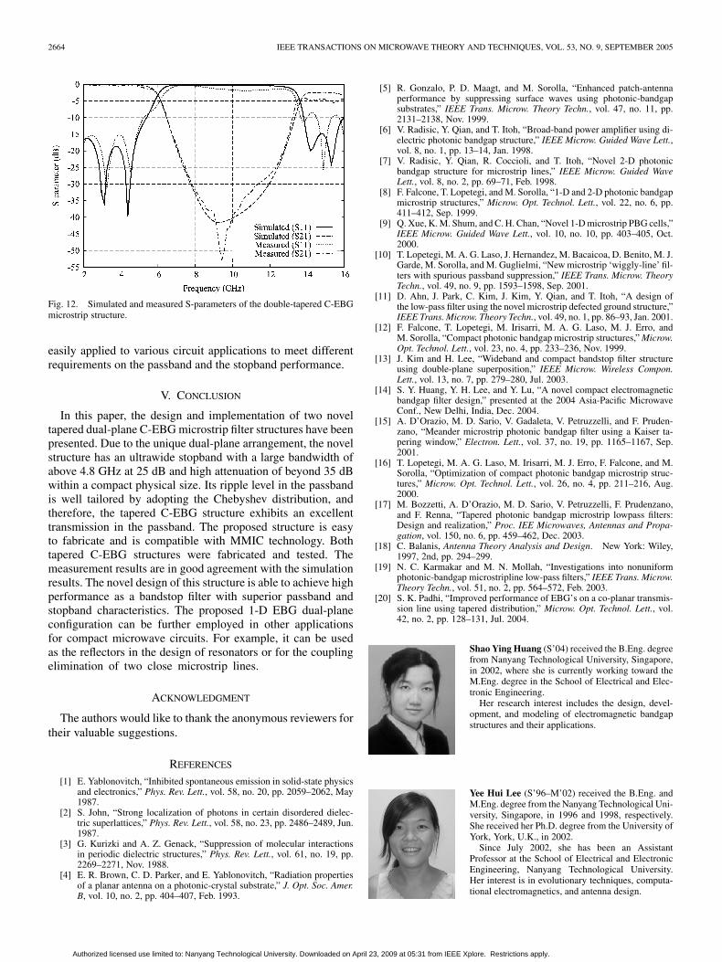
Fig. 9. Simulated S-parameters of the tapered and uniform dual-plane C-EBGmicrostrip structure. (a) S . (b) S .
In the same figure, the double-tapered C-EBG structure ex-hibits a stopband with a 25-dB bandwidth of 5.05 dB and anattenuation of 41.54 dB. Its ripple level in the lower passband is
Authorized licensed use limited to: Nanyang Technological University. Downloaded on April 23, 2009 at 05:31 from IEEE Xplore. Restrictions apply.

HUANG AND LEE: TAPERED DUAL-PLANE COMPACT ELECTROMAGNETIC BANDGAP MICROSTRIP FILTER STRUCTURES 2663
0.16 dB whereas that in the higher passband is 3.20 dB. Com-paring the double-tapered C-EBG structure to the ground-ta-pered C-EBG structure, its performance is improved in termsof ripple levels in both passbands. However, the bandwidth andattenuation of its stopband are reduced. Although the stopbandperformances of both tapered C-EBG structures are degraded,their bandwidth and attenuation are still larger than those inthe single-plane EBG structures (Fig. 4). Fig. 9(b) shows their
parameters. It is observed that both tapered C-EBG struc-tures show much lower sidelobe levels than those of the uni-form structure, which implies the smooth transmission in thepassband. The double-tapered C-EBG structure has the best per-formance of the three structures in terms of ripple level in thepassband while its stopband performance is the worst.
As revealed by the results above, the ripple level of the pro-posed C-EBG structure can be tailored by applying a taperingtechnique to taper the dimension of EBG units on differentplanes, which comes with degradation of the stopband perfor-mance. A double-tapered C-EBG structure is able to obtain alower ripple level than that shown in a single tapered C-EBGstructure such as the ground-tapered C-EBG structure. With theunique dual-plane configuration, the filtering functionality ofthe proposed C-EBG structure can be adjusted to meet differentrequirements in various applications.
B. Measurement Results
Both the proposed ground-tapered and double-taperedfive-patch six-circle dual-plane C-EBG microstrip structurewere fabricated and tested. Fig. 10(a) and (b) shows the mod-ulated microstrip line and the ground plane with etched circlesof the fabricated structures, respectively. These structures arehighly compact with a dimension of 70 mm by 26 mm as shownin Fig. 10. Figs. 11 and 12, show the simulated and measuredS-parameters of the fabricated ground-tapered C-EBG structureand double-tapered C-EBG structure, respectively. As can beseen from the measurement results in the two figures, with onlysix EBG cells, the ground-tapered C-EBG structure is able toachieve a 25-dB bandwidth of 5.98 GHz at 10 GHz, with anattenuation of 39.00 dB, a ripple level of 1.56 dB in the lowerpassband, and a ripple level of 4.68 dB in the higher pass-band whereas the fabricated double-tapered C-EBG structureexhibits a 25-dB bandwidth of 4.87 GHz, an attenuation of52.9 dB, a ripple level of 0.51 dB in the lower passband, anda ripple level of 5.47 dB in the higher passband. An excellentagreement between the measurement and the simulation resultshave been obtained in both the proposed tapered dual-planeC-EBG structures. The slight difference is probably due to theeffect of SMA connectors, the lack of material uniformity andcell uniformity, the over etching, and the nonideal soldering.The infinite ground plane assumed in the simulation is anotherpossible cause for the difference.
Both proposed tapered dual-plane C-EBG structures demon-strate the advantages of large bandwidth, high attenuation,smooth passband, compact size, and easy fabrication process.The ground-tapered C-EBG structure is able to obtain an ultra-wide stopband with very high attenuation and relatively smallripple levels in both passbands whereas the double-taperedC-EBG structure shows an extremely small ripple level inthe passband but a relatively smaller stopband bandwidth and
Fig. 10. Photographs of the fabricated ground-tapered dual-plane C-EBGmicrostrip structure (upper) and the fabricated double-tapered dual-planeC-EBG microstrip structure (lower). (a) Microstrip line. (b) Ground plane.
Fig. 11. Simulated and measured S-parameters of the ground-tapered C-EBGmicrostrip structure.
attenuation. Due to their common characteristics and the uniquefeature of each structure, these two proposed structures can be
Authorized licensed use limited to: Nanyang Technological University. Downloaded on April 23, 2009 at 05:31 from IEEE Xplore. Restrictions apply.
2664 IEEE TRANSACTIONS ON MICROWAVE THEORY AND TECHNIQUES, VOL. 53, NO. 9, SEPTEMBER 2005
Fig. 12. Simulated and measured S-parameters of the double-tapered C-EBGmicrostrip structure.
easily applied to various circuit applications to meet differentrequirements on the passband and the stopband performance.
V. CONCLUSION
In this paper, the design and implementation of two noveltapered dual-plane C-EBG microstrip filter structures have beenpresented. Due to the unique dual-plane arrangement, the novelstructure has an ultrawide stopband with a large bandwidth ofabove 4.8 GHz at 25 dB and high attenuation of beyond 35 dBwithin a compact physical size. Its ripple level in the passbandis well tailored by adopting the Chebyshev distribution, andtherefore, the tapered C-EBG structure exhibits an excellenttransmission in the passband. The proposed structure is easyto fabricate and is compatible with MMIC technology. Bothtapered C-EBG structures were fabricated and tested. Themeasurement results are in good agreement with the simulationresults. The novel design of this structure is able to achieve highperformance as a bandstop filter with superior passband andstopband characteristics. The proposed 1-D EBG dual-planeconfiguration can be further employed in other applicationsfor compact microwave circuits. For example, it can be usedas the reflectors in the design of resonators or for the couplingelimination of two close microstrip lines.
ACKNOWLEDGMENT
The authors would like to thank the anonymous reviewers fortheir valuable suggestions.
REFERENCES
[1] E. Yablonovitch, “Inhibited spontaneous emission in solid-state physicsand electronics,” Phys. Rev. Lett., vol. 58, no. 20, pp. 2059–2062, May1987.
[2] S. John, “Strong localization of photons in certain disordered dielec-tric superlattices,” Phys. Rev. Lett., vol. 58, no. 23, pp. 2486–2489, Jun.1987.
[3] G. Kurizki and A. Z. Genack, “Suppression of molecular interactionsin periodic dielectric structures,” Phys. Rev. Lett., vol. 61, no. 19, pp.2269–2271, Nov. 1988.
[4] E. R. Brown, C. D. Parker, and E. Yablonovitch, “Radiation propertiesof a planar antenna on a photonic-crystal substrate,” J. Opt. Soc. Amer.B, vol. 10, no. 2, pp. 404–407, Feb. 1993.
[5] R. Gonzalo, P. D. Maagt, and M. Sorolla, “Enhanced patch-antennaperformance by suppressing surface waves using photonic-bandgapsubstrates,” IEEE Trans. Microw. Theory Techn., vol. 47, no. 11, pp.2131–2138, Nov. 1999.
[6] V. Radisic, Y. Qian, and T. Itoh, “Broad-band power amplifier using di-electric photonic bandgap structure,” IEEE Microw. Guided Wave Lett.,vol. 8, no. 1, pp. 13–14, Jan. 1998.
[7] V. Radisic, Y. Qian, R. Coccioli, and T. Itoh, “Novel 2-D photonicbandgap structure for microstrip lines,” IEEE Microw. Guided WaveLett., vol. 8, no. 2, pp. 69–71, Feb. 1998.
[8] F. Falcone, T. Lopetegi, and M. Sorolla, “1-D and 2-D photonic bandgapmicrostrip structures,” Microw. Opt. Technol. Lett., vol. 22, no. 6, pp.411–412, Sep. 1999.
[9] Q. Xue, K. M. Shum, and C. H. Chan, “Novel 1-D microstrip PBG cells,”IEEE Microw. Guided Wave Lett., vol. 10, no. 10, pp. 403–405, Oct.2000.
[10] T. Lopetegi, M. A. G. Laso, J. Hernandez, M. Bacaicoa, D. Benito, M. J.Garde, M. Sorolla, and M. Guglielmi, “New microstrip ‘wiggly-line’ fil-ters with spurious passband suppression,” IEEE Trans. Microw. TheoryTechn., vol. 49, no. 9, pp. 1593–1598, Sep. 2001.
[11] D. Ahn, J. Park, C. Kim, J. Kim, Y. Qian, and T. Itoh, “A design ofthe low-pass filter using the novel microstrip defected ground structure,”IEEE Trans. Microw. Theory Techn., vol. 49, no. 1, pp. 86–93, Jan. 2001.
[12] F. Falcone, T. Lopetegi, M. Irisarri, M. A. G. Laso, M. J. Erro, andM. Sorolla, “Compact photonic bandgap microstrip structures,” Microw.Opt. Technol. Lett., vol. 23, no. 4, pp. 233–236, Nov. 1999.
[13] J. Kim and H. Lee, “Wideband and compact bandstop filter structureusing double-plane superposition,” IEEE Microw. Wireless Compon.Lett., vol. 13, no. 7, pp. 279–280, Jul. 2003.
[14] S. Y. Huang, Y. H. Lee, and Y. Lu, “A novel compact electromagneticbandgap filter design,” presented at the 2004 Asia-Pacific MicrowaveConf., New Delhi, India, Dec. 2004.
[15] A. D’Orazio, M. D. Sario, V. Gadaleta, V. Petruzzelli, and F. Pruden-zano, “Meander microstrip photonic bandgap filter using a Kaiser ta-pering window,” Electron. Lett., vol. 37, no. 19, pp. 1165–1167, Sep.2001.
[16] T. Lopetegi, M. A. G. Laso, M. Irisarri, M. J. Erro, F. Falcone, and M.Sorolla, “Optimization of compact photonic bandgap microstrip struc-tures,” Microw. Opt. Technol. Lett., vol. 26, no. 4, pp. 211–216, Aug.2000.
[17] M. Bozzetti, A. D’Orazio, M. D. Sario, V. Petruzzelli, F. Prudenzano,and F. Renna, “Tapered photonic bandgap microstrip lowpass filters:Design and realization,” Proc. IEE Microwaves, Antennas and Propa-gation, vol. 150, no. 6, pp. 459–462, Dec. 2003.
[18] C. Balanis, Antenna Theory Analysis and Design. New York: Wiley,1997, 2nd, pp. 294–299.
[19] N. C. Karmakar and M. N. Mollah, “Investigations into nonuniformphotonic-bandgap microstripline low-pass filters,” IEEE Trans. Microw.Theory Techn., vol. 51, no. 2, pp. 564–572, Feb. 2003.
[20] S. K. Padhi, “Improved performance of EBG’s on a co-planar transmis-sion line using tapered distribution,” Microw. Opt. Technol. Lett., vol.42, no. 2, pp. 128–131, Jul. 2004.
Shao Ying Huang (S’04) received the B.Eng. degreefrom Nanyang Technological University, Singapore,in 2002, where she is currently working toward theM.Eng. degree in the School of Electrical and Elec-tronic Engineering.
Her research interest includes the design, devel-opment, and modeling of electromagnetic bandgapstructures and their applications.
Yee Hui Lee (S’96–M’02) received the B.Eng. andM.Eng. degree from the Nanyang Technological Uni-versity, Singapore, in 1996 and 1998, respectively.She received her Ph.D. degree from the University ofYork, York, U.K., in 2002.
Since July 2002, she has been an AssistantProfessor at the School of Electrical and ElectronicEngineering, Nanyang Technological University.Her interest is in evolutionary techniques, computa-tional electromagnetics, and antenna design.
Authorized licensed use limited to: Nanyang Technological University. Downloaded on April 23, 2009 at 05:31 from IEEE Xplore. Restrictions apply.