2:8 differential lvpecl/lvecl/hstl clock and data driver · input select truth table l h clk0, clk0...
TRANSCRIPT

General DescriptionThe MAX9325 low-skew, 2:8 differential driver featuresextremely low output-to-output skew (50ps max) andpart-to-part skew (225ps max). These features makethe device ideal for clock and data distribution across abackplane or board. The device selects one of the twodifferential HSTL or LVECL/LVPECL inputs and repeatsthem at eight differential outputs. Outputs are compati-ble with LVECL and LVPECL, and can directly drive50Ω terminated transmission lines.
The differential inputs can be configured to accept asingle-ended signal when the unused complementaryinput is connected to the on-chip reference output volt-age VBB. All inputs have internal pulldown resistors toVEE. The internal pulldowns and a fail-safe circuitensure differential low default outputs when the inputsare left open or at VEE.
The MAX9325 operates over a 2.375V to 3.8V supplyrange for interfacing to differential HSTL and LVPECLsignals. This allows high-performance clock or data dis-tribution in systems with a nominal +2.5V or +3.3V sup-ply. For LVECL operation, the device operates with a-2.375V to -3.8V supply.
The MAX9325 is offered in 28-lead PLCC and space-saving 28-lead QFN packages. The MAX9325 is speci-fied for operation from -40°C to +85°C.
ApplicationsPrecision Clock Distribution
Low-Jitter Data Repeaters
Features♦ 50ps (max) Output-to-Output Skew
♦ 1.5psRMS (max) Random Jitter
♦ Guaranteed 300mV Differential Output at 700MHz
♦ +2.375V to +3.8V Supplies for DifferentialHSTL/LVPECL
♦ -2.375V to -3.8V Supplies for Differential LVECL
♦ Two Selectable Differential Inputs
♦ On-Chip Reference for Single-Ended Inputs
♦ Outputs Low for Inputs Open or at VEE
♦ Pin Compatible with MC100LVE310
MA
X9
32
5
2:8 Differential LVPECL/LVECL/HSTL Clock andData Driver
________________________________________________________________ Maxim Integrated Products 1
28 27 26 25 24 23 22
Q0 Q0 Q1 V CC
Q1 Q2 Q2
8 9 10 11 12 13 14
N.C. Q7 V CC Q7 Q6 Q6
15
16
17
18
19
20
21
Q5
*CORNER PINS AND EXPOSED PAD ARE CONNECTED TO VEE.
Q5
Q4
VCC
Q4
Q3
Q3
7
6
5
4
3
2
1
CLK1
VBB
VCC
CLKO
CLK_SEL
VEE
MAX9325
QFN
Q0 Q1 V CC
Q2
N.C.
V CC Q7 Q6
Q5
VCC
Q4
Q3
CLK1
VBB
VCC
CLKO
CLK_SEL
VEE
Q5
Q4
Q3
CLKO
CLKO
CLK1
CLK1
Q7 Q6
Q2Q1Q0
PLCC
TOP VIEW
5 6 7 8 9 10 11
22232425 192021
12
13
14
15
16
17
1826
27
28
1
2
3
4
MAX9325
* *
** CLK_SEL INPUT CLOCK
INPUT SELECT TRUTH TABLE
L
H
CLK0, CLK0 SELECTED
CLK1, CLK1 SELECTED
Pin Configurations
Ordering Information
19-2511; Rev 3; 11/04
For pricing, delivery, and ordering information, please contact Maxim/Dallas Direct! at 1-888-629-4642, or visit Maxim’s website at www.maxim-ic.com.
Functional Diagram appears at end of data sheet.
PART TEMP RANGE PIN-PACKAGE
MAX9325EQI -40°C to +85°C 28 PLCC
MAX9325EGI -40°C to +85°C 28 QFN 5mm x 5mm
MA
X9
32
5
2:8 Differential LVPECL/LVECL/HSTL Clock andData Driver
2 _______________________________________________________________________________________
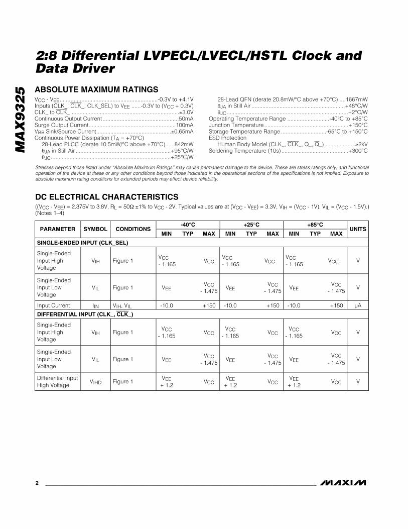
ABSOLUTE MAXIMUM RATINGS
DC ELECTRICAL CHARACTERISTICS((VCC - VEE) = 2.375V to 3.8V, RL = 50Ω ±1% to VCC - 2V. Typical values are at (VCC - VEE) = 3.3V, VIH = (VCC - 1V), VIL = (VCC - 1.5V).)(Notes 1–4)
Stresses beyond those listed under “Absolute Maximum Ratings” may cause permanent damage to the device. These are stress ratings only, and functionaloperation of the device at these or any other conditions beyond those indicated in the operational sections of the specifications is not implied. Exposure toabsolute maximum rating conditions for extended periods may affect device reliability.
VCC - VEE...............................................................-0.3V to +4.1VInputs (CLK_, CLK_, CLK_SEL) to VEE ......-0.3V to (VCC + 0.3V)CLK_ to CLK_ .....................................................................±3.0VContinuous Output Current .................................................50mASurge Output Current........................................................100mAVBB Sink/Source Current................................................±0.65mAContinuous Power Dissipation (TA = +70°C)
28-Lead PLCC (derate 10.5mW/°C above +70°C) .....842mWθJA in Still Air .............................................................+95°C/WθJC.............................................................................+25°C/W
28-Lead QFN (derate 20.8mW/°C above +70°C) ....1667mWθJA in Still Air ............................................................+48°C/WθJC..............................................................................+2°C/W
Operating Temperature Range ...........................-40°C to +85°CJunction Temperature ......................................................+150°CStorage Temperature Range .............................-65°C to +150°CESD Protection
Human Body Model (CLK_, CLK_, Q_, Q_)....................≥2kVSoldering Temperature (10s) ...........................................+300°C
-40°C +25°C +85°CPARAMETER SYMBOL CONDITIONS
MIN TYP MAX MIN TYP MAX MIN TYP MAXUNITS
SINGLE-ENDED INPUT (CLK_SEL)
Single-EndedInput HighVoltage
VIH Figure 1VCC- 1.165
VCCVCC- 1.165
VCCVCC- 1.165
VCC V
Single-EndedInput LowVoltage
VIL Figure 1 VEEVCC
- 1.475VEE
VCC- 1.475
VEEVCC
- 1.475V
Input Current IIN VIH, VIL -10.0 +150 -10.0 +150 -10.0 +150 µA
DIFFERENTIAL INPUT (CLK_, CLK_)
Single-EndedInput HighVoltage
VIH Figure 1VCC
- 1.165VCC
VCC- 1.165
VCCVCC
- 1.165VCC V
Single-EndedInput LowVoltage
VIL Figure 1 VEEVCC
- 1.475VEE
VCC- 1.475
VEEVCC
- 1.475V
Differential InputHigh Voltage
VIHD Figure 1VEE
+ 1.2VCC
VEE+ 1.2
VCCVEE
+ 1.2VCC V

MA
X9
32
5
2:8 Differential LVPECL/LVECL/HSTL Clock andData Driver
_______________________________________________________________________________________ 3
DC ELECTRICAL CHARACTERISTICS (continued)((VCC - VEE) = 2.375V to 3.8V, RL = 50Ω ±1% to VCC - 2V. Typical values are at (VCC - VEE) = 3.3V, VIH = (VCC - 1V), VIL = (VCC - 1.5V).)(Notes 1–4)
-40°C +25°C +85°CPARAMETER SYMBOL CONDITIONS
MIN TYP MAX MIN TYP MAX MIN TYP MAXUNITS
Differential InputLow Voltage
VILD Figure 1 VEEVCC
- 0.095VEE
VCC- 0.095
VEEVCC
- 0.095V
(VCC - VEE) <3.0V, Figure 1
0.095VCC- VEE
0.095VCC- VEE
0.095VCC- VEEDifferential Input
VoltageVIHD -
VILD (VCC - VEE) ≥3.0V, Figure 1
0.095 3.0 0.095 3.0 0.095 3.0V
Input Current IINVIH, VIL, VIHD,
VILD-10.0 +150.0 -10.0 +150.0 -10.0 +150.0 µA
OUTPUT (Q_, Q_)
Single-EndedOutput HighVoltage
VOH Figure 2VCC
- 1.085VCC
- 0.977VCC
- 0.880VCC
- 1.025VCC
- 0.949VCC
- 0.88VCC
- 1.025VCC
- 0.929VCC
- 0.88V
Single-EndedOutput LowVoltage
VOL Figure 2VCC
- 1.810VCC
- 1.695VCC
- 1.620VCC
- 1.810VCC
- 1.697VCC
- 1.62VCC
- 1.810VCC
- 1.698VCC
- 1.62V
DifferentialOutput Voltage
VOH - VOL Figure 2 535 718 595 749 595 769 mV
REFERENCE VOLTAGE OUTPUT (VBB)
ReferenceVoltage Output
VBBIBB = ±0.5mA(Note 5)
VCC- 1.38
VCC- 1.318
VCC- 1.26
VCC- 1.38
VCC- 1.325
VCC- 1.26
VCC- 1.38
VCC- 1.328
VCC- 1.26
V
SUPPLY
Supply Current IEE (Note 6) 35 50 39 55 42 65 mA

MA
X9
32
5
2:8 Differential LVPECL/LVECL/HSTL Clock andData Driver
4 _______________________________________________________________________________________
AC ELECTRICAL CHARACTERISTICS—PLCC Package((VCC - VEE) = 2.375V to 3.8V, RL = 50Ω ±1% to VCC - 2V, fIN ≤ 500MHz, input transition time = 125ps (20% to 80%). Typical valuesare at (VCC - VEE) = 3.3V, VIH = (VCC - 1V), VIL = (VCC - 1.5V).) (Note 7)
-40°C +25°C +85°CPARAMETER SYMBOL CONDITIONS
MIN TYP MAX MIN TYP MAX MIN TYP MAXUNITS
DifferentialInput-to-OutputDelay
tPLHDtPHLD
Figure 2 525 725 550 750 575 775 ps
Single-EndedInput-to-OutputDelay
tPLHtPHL
Figure 3 (Note 8) 500 750 550 800 600 850 ps
Output-to-Output Skew
tSKOO (Note 9) 50 50 50 ps
Part-to-PartSkew
tSKPPDifferential input(Note 10) 160 190 225 ps
Added RandomJitter
tRJ
fIN = 0.5GHzclock pattern(Note 11)
1.5 1.5 1.5 psRMS
AddedDeterministicJitter
tDJ
fIN = 1.0Gbps,2E23 - 1 PRBSpattern (Note 11)
100 100 100 psP-P
SwitchingFrequency
fMAX
VOH - VOL ≥300mV clockpattern
1.5 1.5 1.5 GHz
Output Rise/FallTime (20% to80%)
tR, tF Figure 2 140 440 140 440 140 440 ps

MA
X9
32
5
2:8 Differential LVPECL/LVECL/HSTL Clock andData Driver
_______________________________________________________________________________________ 5
AC ELECTRICAL CHARACTERISTICS—QFN Package((VCC - VEE) = 2.375V to 3.8V, RL = 50Ω ±1% to VCC - 2V, fIN ≤ 500MHz, input transition time = 125ps (20% to 80%). Typical valuesare at (VCC - VEE) = 3.3V, VIH = (VCC - 1V), VIL = (VCC - 1.5V).) (Note 7)
-40°C +25°C +85°CPARAMETER SYMBOL CONDITIONS
MIN TYP MAX MIN TYP MAX MIN TYP MAXUNITS
DifferentialInput-to-OutputDelay
tPLHDtPHLD
Figure 2 250 575 298 553 309 576 ps
Single-EndedInput-to-OutputDelay
tPLHtPHL
Figure 3 (Note 8) 253 581 310 586 324 606 ps
Output-to-Output Skew
tSKOO (Note 9) 50 50 50 ps
Part-to-PartSkew
tSKPPDifferential input(Note 10) 192 215 218 ps
Added RandomJitter
tRJ
fIN = 0.5GHzclock pattern(Note 11)
1.5 1.5 1.5 psRMS
AddedDeterministicJitter
tDJ
fIN = 1.0Gbps,2E23 - 1 PRBSpattern (Note 11)
95 95 95 psP-P
SwitchingFrequency
fMAX
VOH - VOL ≥300mV clockpattern
1.5 1.5 1.5 GHz
Output Rise/FallTime (20% to80%)
tR, tF Figure 2 97 411 104 210 111 232 ps
Note 1: Measurements are made with the device in thermal equilibrium.Note 2: Current into a pin is defined as positive. Current out of a pin is defined as negative.Note 3: DC parameters production tested at TA = +25°C and guaranteed by design over the full operating temperature range.Note 4: Single-ended input operation using VBB is limited to (VCC - VEE) = 3.0V to 3.8V.Note 5: Use VBB only for inputs that are on the same device as the VBB reference.Note 6: All pins open except VCC and VEE.Note 7: Guaranteed by design and characterization. Limits are set at ±6 sigma.Note 8: Measured from the 50% point of the input signal with the 50% point equal to VBB, to the 50% point of the output signal.Note 9: Measured between outputs of the same part at the signal crossing points for a same-edge transition. Differential input signal.Note 10: Measured between outputs of different parts under identical condition for same-edge transition.Note 11: Device jitter added to the input signal. Differential input signal.

MA
X9
32
5
2:8 Differential LVPECL/LVECL/HSTL Clock andData Driver
6 _______________________________________________________________________________________
SUPPLY CURRENT (IEE)vs. TEMPERATURE
MAX
9325
toc0
1
TEMPERATURE (°C)
SUPP
LY C
URRE
NT (m
A)
603510-15
25
30
35
40
45
50
20-40 85
OUTPUT AMPLITUDE (VOH - VOL)vs. FREQUENCY
MAX
9325
toc0
2
FREQUENCY (MHz)
OUTP
UT V
OLTA
GE (V
)1000 1500500
300
500
400
600
700
800
0
TRANSITION TIME vs. TEMPERATURE
TRAN
SITI
ON T
IME
(ps)
160
240
200
280
320
360
400
MAX
9325
toc0
3
TEMPERATURE (°C)603510-15-40 85
tF
tR
PROPAGATION DELAYvs. TEMPERATURE
MAX
9325
toc0
5
TEMPERATURE (°C)603510-15
550
650
750
450-40 85
PROP
AGAT
ION
DELA
Y (p
s)
tPLHD
tPHLD
Typical Operating Characteristics(PLCC package, typical values are at (VCC - VEE) = 3.3V, VIH = (VCC - 1V), VIL = (VCC - 1.5V), RL = 50Ω ±1% to VCC - 2V, fIN =500MHz, input transition time = 125ps (20% to 80%).)

MA
X9
32
5
2:8 Differential LVPECL/LVECL/HSTL Clock andData Driver
_______________________________________________________________________________________ 7
Pin Description
PINPLCC QFN
NAME FUNCTION
1, 8, 15, 22 4, 11, 18, 25 VCC
Positive Supply Voltage. Bypass each VCC to VEE with 0.1µF and 0.01µF ceramiccapacitors. Place the capacitors as close to the device as possible, with the smallervalue capacitor closest to the device.
2 5 CLK0 Inverting Differential Clock Input 0. Internal 105kΩ pulldown to VEE.
3 6 VBB
Reference Output Voltage. Connect to the inverting or noninverting clock input toprovide a reference for single-ended operation. When used, bypass VBB to VCC with a0.01µF ceramic capacitor. Otherwise leave open.
4 7 CLK1 Noninverting Differential Clock Input 1. Internal 105kΩ pulldown to VEE.
5 8 CLK1 Inverting Differential Clock Input 1. Internal 105kΩ pulldown to VEE.
6 9 N.C. Not Connected
7 10 Q7 Inverting Q7 Output. Typically terminate with 50Ω resistor to VCC - 2V.
9 12 Q7 Noninverting Q7 Output. Typically terminate with 50Ω resistor to VCC - 2V.
10 13 Q6 Inverting Q6 Output. Typically terminate with 50Ω resistor to VCC - 2V.
11 14 Q6 Noninverting Q6 Output. Typically terminate with 50Ω resistor to VCC - 2V.
12 15 Q5 Inverting Q5 Output. Typically terminate with 50Ω resistor to VCC - 2V.
13 16 Q5 Noninverting Q5 Output. Typically terminate with 50Ω resistor to VCC - 2V.
14 17 Q4 Inverting Q4 Output. Typically terminate with 50Ω resistor to VCC - 2V.
16 19 Q4 Noninverting Q4 Output. Typically terminate with 50Ω resistor to VCC - 2V.
17 20 Q3 Inverting Q3 Output. Typically terminate with 50Ω resistor to VCC - 2V.
18 21 Q3 Noninverting Q3 Output. Typically terminate with 50Ω resistor to VCC - 2V.
19 22 Q2 Inverting Q2 Output. Typically terminate with 50Ω resistor to VCC - 2V.
20 23 Q2 Noninverting Q2 Output. Typically terminate with 50Ω resistor to VCC - 2V.
21 24 Q1 Inverting Q1 Output. Typically terminate with 50Ω resistor to VCC - 2V.
23 26 Q1 Noninverting Q1 Output. Typically terminate with 50Ω resistor to VCC - 2V.
24 27 Q0 Inverting Q0 Output. Typically terminate with 50Ω resistor to VCC - 2V.
25 28 Q0 Noninverting Q0 Output. Typically terminate with 50Ω resistor to VCC - 2V.
26 1 VEE Negative Supply Voltage
27 2 CLK_SELClock Select Input. When driven low, the CLK0 input is selected. Drive high to selectthe CLK1 Input. The CLK_SEL threshold is equal to VBB. Internal 75kΩ pulldown to VEE.
28 3 CLK0 Noninverting Differential Clock Input 0. Internal 105kΩ pulldown to VEE.
ExposedExposed
Pad— Internally Connected to VEE

MA
X9
32
5
2:8 Differential LVPECL/LVECL/HSTL Clock andData Driver
8 _______________________________________________________________________________________
DIFFERENTIAL INPUT VOLTAGE DEFINITION
VCC VCC
VILD (MAX)
VIHD (MAX)
VILD (MIN)
VIHD (MIN)
VEE VEE
VBB
VIH
VIL
VIHD - VILD
SINGLE-ENDED INPUT VOLTAGE DEFINITION
VIHD - VILD
Figure 1. Input Voltage Definitions
CLK
CLK
Q_
Q_
Q_ - Q_
20%20%
80%80%
VIHD - VILD
VOH - VOL
VOH - VOL
VOH - VOL
DIFFERENTIAL OUTPUT WAVEFORM
0V (DIFFERENTIAL)
VIHD
VILD
VOH
VOL
tPLHD
tR tF
tPHLD
Figure 2. Differential Input (CLK_, CLK_) to Output (Q_, Q_) Delay Timing Diagram

MA
X9
32
5
2:8 Differential LVPECL/LVECL/HSTL Clock andData Driver
_______________________________________________________________________________________ 9
Detailed DescriptionThe MAX9325 low-skew, 2:8 differential driver featuresextremely low output-to-output skew (50ps max) andpart-to-part skew (225ps max). These features make thedevice ideal for clock and data distribution across abackplane or board. The device selects one of the twodifferential HSTL or LVECL/LVPECL inputs, and repeatsthem at eight differential outputs. Outputs are compati-ble with LVECL and LVPECL, and can directly drive 50Ωterminated transmission lines.
A 2:1 mux selects between the two differential inputs,CLK0, CLK0 and CLK1, CLK1. The 2:1 mux is switchedby the single-ended CLK_SEL input. A logic low selectsthe CLK0, CLK0 input. A logic high selects the CLK1,CLK1 input. The logic threshold for CLK_SEL is set byan internal VBB voltage reference. The selected input isreproduced at eight differential outputs at speeds up to700MHz.
The differential inputs can be configured to accept asingle-ended signal when the unused complementaryinput is connected to the on-chip reference output volt-age (VBB). A single-ended input of at least VBB ±95mVor a differential input of at least 95mV switches the out-puts to the VOH and VOL levels specified in the DCElectrical Characteristics. The maximum magnitude ofthe differential input from CLK_ to CLK_ is ±3.0V or
±(VCC - VEE), whichever is less. This limit also appliesto the difference between a single-ended input and anyreference voltage input.
The single-ended CLK_SEL input has a 75kΩ pulldownto VEE that selects the default input, CLK0, CLK0, whenCLK_SEL is left open or at VEE. All the differential inputshave 105kΩ pulldowns to VEE. Internal pulldowns and afail-safe circuit ensure differential low default outputswhen the inputs are left open or at VEE.
Specifications for the high and low voltages of a differ-ential input (VIHD and VILD) and the differential inputvoltage (VIHD - VILD) apply simultaneously.
For interfacing to differential HSTL and LVPECL signals,these devices operate over a +2.375V to +3.8V supplyrange, allowing high-performance clock or data distrib-ution in systems with a nominal +2.5V or +3.3V supply.For differential LVECL operation, these devices operatefrom a -2.375V to -3.8V supply.
Single-Ended OperationCLK_SEL is a single-ended input with the input thresholdinternally set to VBB, and can be driven to VCC or VEE orby a single-ended LVPECL/LVECL signal. The CLK_,CLK_ are differential inputs but can be configured toaccept single-ended inputs when operating at supplyvoltages greater than 2.58V. The recommended supplyvoltage for single-ended operation is 3.0V to 3.8V. A dif-
OR
VBB
VBB
VBB
VBB
tPLH tPHL
VOH - VOL
Q_
Q_
CLK_ WHEN CLK_ = VBB
VOH
VIL
VIL
VIH
VIH
VOL
CLK_ WHEN CLK_ = VBB
Figure 3. Single-Ended Input (CLK_, CLK_) to Output (Q_, Q_) Delay Timing Diagram

MA
X9
32
5
2:8 Differential LVPECL/LVECL/HSTL Clock andData Driver
10 ______________________________________________________________________________________
ferential input is configured for single-ended operationby connecting the on-chip reference voltage, VBB, to anunused complementary input as a reference. For exam-ple, the differential CLK0, CLK0 input is converted to anoninverting, single-ended input by connecting VBB toCLK0 and connecting the single-ended input to CLK0.Similarly, an inverting input is obtained by connectingVBB to CLK0 and connecting the single-ended input toCLK0. With a differential input configured as single-ended (using VBB), the single-ended input can be drivento VCC or VEE or with a single-ended LVPECL/LVECLsignal.
When configuring a differential input as a single-endedinput, a user must ensure that the supply voltage (VCC -VEE) is greater than 2.58V. This is because the inputhigh minimum level must be at (VEE + 1.2V) or higherfor proper operation. The reference voltage VBB mustbe at least (VEE + 1.2V) or higher for the same reasonbecause it becomes the high-level input when the othersingle-ended input swings below it. The minimum VBBoutput for the MAX9325 is (VCC - 1.38V). Substitutingthe minimum VBB output for (VBB = VEE + 1.2V) resultsin a minimum supply (VCC - VEE) of 2.58V. Rounding upto standard supplies gives the single-ended operatingsupply ranges (VCC - VEE ) of 3.0V to 3.8V for theMAX9325.
When using the VBB reference output, bypass it with a0.01µF ceramic capacitor to VCC. If not used, leave itopen. The VBB reference can source or sink 0.5mA,which is sufficient to drive two inputs.
Applications InformationOutput Termination
Terminate the outputs through 50Ω to (VCC - 2V) or useequivalent Thevenin terminations. Terminate each Q andQ output with identical termination on each for low outputdistortion. When a single-ended signal is taken from thedifferential output, terminate both Q_ and Q_.
Ensure that output currents do not exceed the currentlimits as specified in the Absolute Maximum Ratingstable. Under all operating conditions, the device’s totalthermal limits should be observed.
Supply BypassingBypass each VCC to VEE with high-frequency surface-mount ceramic 0.1µF and 0.01µF capacitors. Place thecapacitors as close to the device as possible with the0.01µF capacitor closest to the device pins.
Use multiple vias when connecting the bypass capaci-tors to ground. When using the VBB reference output,bypass it with a 0.01µF ceramic capacitor to VCC. If theVBB reference is not used, it can be left open.
TracesCircuit board trace layout is very important to maintainthe signal integrity of high-speed differential signals.Maintaining integrity is accomplished in part by reduc-ing signal reflections and skew, and increasing com-mon-mode noise immunity.
Signal reflections are caused by discontinuities in the50Ω characteristic impedance of the traces. Avoid dis-continuities by maintaining the distance between differ-ential traces, not using sharp corners or using vias.Maintaining distance between the traces also increasescommon-mode noise immunity. Reducing signal skewis accomplished by matching the electrical length ofthe differential traces.
Exposed-Pad PackageThe 28-lead QFN package (MAX9325EGI) has theexposed paddle on the bottom of the package that pro-vides the primary heat removal path from the IC to thePC board, as well as excellent electrical grounding tothe PC board. The MAX9325EGI’s exposed pad isinternally connected to VEE. Do not connect theexposed pad to a separate circuit ground planeunless VEE and the circuit ground are the same.
Chip InformationTRANSISTOR COUNT: 1030
PROCESS: Bipolar
Q0
Q0
Q1
Q1
Q2
Q2
Q3
Q3
Q4
Q4
Q5
0
1
Q5
Q6
Q6
Q7
Q7
VEE
VEE
CLK1
CLK_SEL
CLK1
105kΩ
75kΩ
VEE
CLK0
CLK0
105kΩ
MAX9325
Functional Diagram

MA
X9
32
5
2:8 Differential LVPECL/LVECL/HSTL Clock andData Driver
______________________________________________________________________________________ 11
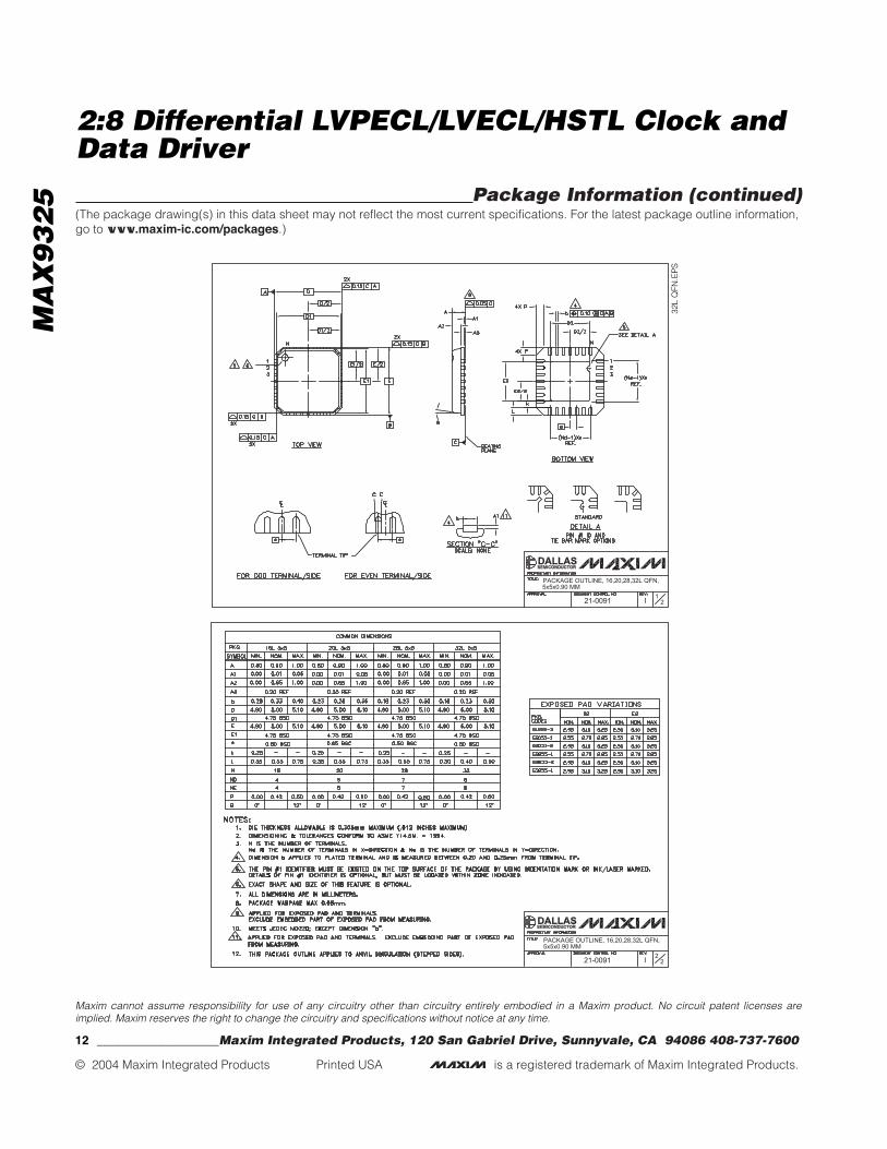
Package Information(The package drawing(s) in this data sheet may not reflect the most current specifications. For the latest package outline information,go to www.maxim-ic.com/packages.)
PLC
C.E
PS
FAMILY PACKAGE OUTLINE: 20L, 28L, 44L, 52L, 68L PLCC
11
21-0049 DREV.DOCUMENT CONTROL NO.APPROVAL
PROPRIETARY INFORMATION
TITLE:
D1
D
C
A2
B1B
A1A
A3 D2
e
D3D1D
D3
N
22.6120.320.800D3
D2 0.890 0.930REF REF
23.62
4.202.293.690.510.330.660.23
9.788.897.375.08
12.3211.439.917.62
17.4016.5114.9912.70
MIN MIN
24.1325.02
0.1200.090A1
REFD3 0.200
0.485
0.300
0.685
0.500
0.985
DD1D2D3
D1D
0.6500.590
0.950
DD1D2D3
0.4500.390
0.6950.6560.630
0.9580.995
REF
0.4950.4560.430REF
0.050
0.385
INCHES
DD1D2
0.3500.290
MIN
A2A3BB1Ce
0.1450.0200.0130.0260.009
0.3950.3560.330
MAX
0.156
0.0210.032
---
0.011
INCHES
A 0.165MIN
0.180MAX
3.04
REF
28
44
68
17.6516.6616.00REF
24.3325.27
12.5711.5810.92REF
AC
AE
AB
10.039.048.38
MAX N20
3.96---0.530.810.28
1.27
AA4.57MAX
NOTES: 1. D1 DOES NOT INCLUDE MOLD FLASH. 2. MOLD FLASH OR PROTRUSIONS NOT TO EXCEED .20mm (.008") PER SIDE. 3. LEADS TO BE COPLANAR WITHIN .10mm. 4. CONTROLLING DIMENSION: MILLIMETER 5. MEETS JEDEC MO047-XX AS SHOWN IN TABLE. 6. N = NUMBER OF PINS.
REFREFD3 0.600 15.2417.5319.0519.94
D1D2
D0.7500.690
0.7850.7560.795
0.730
5219.2020.19
18.54
AD
MA
X9
32
5
2:8 Differential LVPECL/LVECL/HSTL Clock andData Driver
Maxim cannot assume responsibility for use of any circuitry other than circuitry entirely embodied in a Maxim product. No circuit patent licenses areimplied. Maxim reserves the right to change the circuitry and specifications without notice at any time.
12 ____________________Maxim Integrated Products, 120 San Gabriel Drive, Sunnyvale, CA 94086 408-737-7600
© 2004 Maxim Integrated Products Printed USA is a registered trademark of Maxim Integrated Products.
Package Information (continued)(The package drawing(s) in this data sheet may not reflect the most current specifications. For the latest package outline information,go to www.maxim-ic.com/packages.)
32L
QFN
.EP
S