3. overview of microfabrication techniquesevoy/ece658/pdf/chap3.pdf · 3. overview of...
TRANSCRIPT

1
3. Overview of Microfabrication Techniques
The Si Revolution…
First TransistorBell Labs (1947)
Si integrated circuitsTexas Instruments (~1960)
Modern ICs
More ? Check out:http://www.pbs.org/transistor/background1/events/miraclemo.html
http://www.ti.com/corp/docs/company/history/firstic.shtml
The Need of Micropatterning
The batch fabrication of microstructures requires a low-cost, high throughput surface patterning technology
Microfabrication Process
Complete processing sequence consist of:
Layering: OxidationDeposition
Patterning:LithographyEtching
Doping :Ion ImplantationDiffusion
Robotics arm is used to transfer wafers
(Source: IBM)
Check out: B. Van Zeghbroeck, “Principles of Semiconductor Devices ”W. Maly, “Atlas of IC Tech”

2
Again and Again…..
A typical process can have 15-20 masks
Bulk micromachining
Fabrication technologies for the machining of "bulk" microdevices in silicon
Example: Membrane Pressure Sensor Example: MEMS Microturbines

3
3. Overview of Microfabrication…TOC
Wafer-level Processes
SubstratesWafer CleaningOxidationDopingThin-Film DepositionWafer Bonding
3. Overview of Microfabrication…TOC
Pattern Transfer
Optical LithographyDesign RulesMask MakingWet EtchingDry-EtchingLift-OffPlanarization
3. Overview of Microfabrication…TOC
Wafer-level Processes
SubstratesWafer CleaningOxidationDopingThin-Film DepositionWafer Bonding
3. Overview of Microfabrication…TOC
Wafer-level Processes
SubstratesWafer CleaningOxidationDopingThin-Film DepositionWafer Bonding
4
Growth of Silicon (ctnd.)
Quartzite or SiO2 (sand) is reacted in a furnace with carbon (from coke and/or coal) to make metallurgical grade silicon (MGS) which is about 98% pure, via the reaction:
SiO2+2C→Si+2CO
The silicon is crushed and reacted with HCl (gas) to make trichlorosilane:
Si+3HCl(gas)→SiHCl3+H2
Fractional distillation is then used to separate out the SiHCl3 from most of the impurities. The (pure) trichlorosilane is then reacted with hydrogen gas to form pure electronic grade silicon (EGS):
SiHCl3+H2→2Si+3HCl
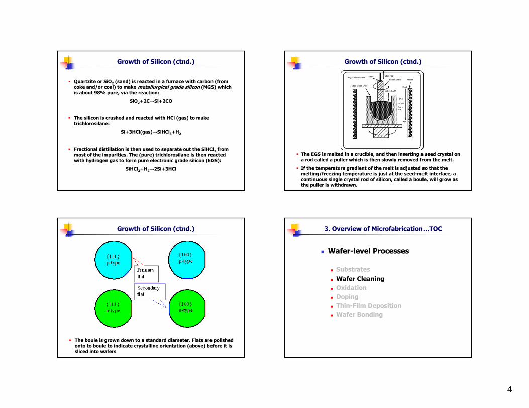
Growth of Silicon (ctnd.)
The EGS is melted in a crucible, and then inserting a seed crystal on a rod called a puller which is then slowly removed from the melt.
If the temperature gradient of the melt is adjusted so that the melting/freezing temperature is just at the seed-melt interface, a continuous single crystal rod of silicon, called a boule, will grow as the puller is withdrawn.
Growth of Silicon (ctnd.)
The boule is grown down to a standard diameter. Flats are polished onto to boule to indicate crystalline orientation (above) before it is sliced into wafers
3. Overview of Microfabrication…TOC
Wafer-level Processes
SubstratesWafer CleaningOxidationDopingThin-Film DepositionWafer Bonding

5
RCA cleaning of Si
The RCA cleaning procedure has three major steps used sequentially:
I. Organic Clean: Removal of insoluble organic contaminants with a 5:1:1 H2O:H2O2:NH4OH solution.
II. Oxide Strip: Removal of a thin silicon dioxide layer where metallic contaminants may accumulated as a result of (I), using a diluted 50:1 H2O:HF solution.
III. Ionic Clean: Removal of ionic and heavy metal atomic contaminants using a solution of 6:1:1 H2O:H2O2: HCl.
3. Overview of Microfabrication…TOC
Wafer-level Processes
SubstratesWafer CleaningOxidationDopingThin-Film DepositionWafer Bonding
Thermal Oxidation
Thermal oxidation of silicon accomplished at high temperatures by flowing oxygen sources such as O2 or H2O
Thermal Oxidation (ctnd.)
Oxidation Reactions
The growth of an oxide layer of thickness x will consume 0.44 x of silicon
x0.44 x
Si Si
SiO2
6
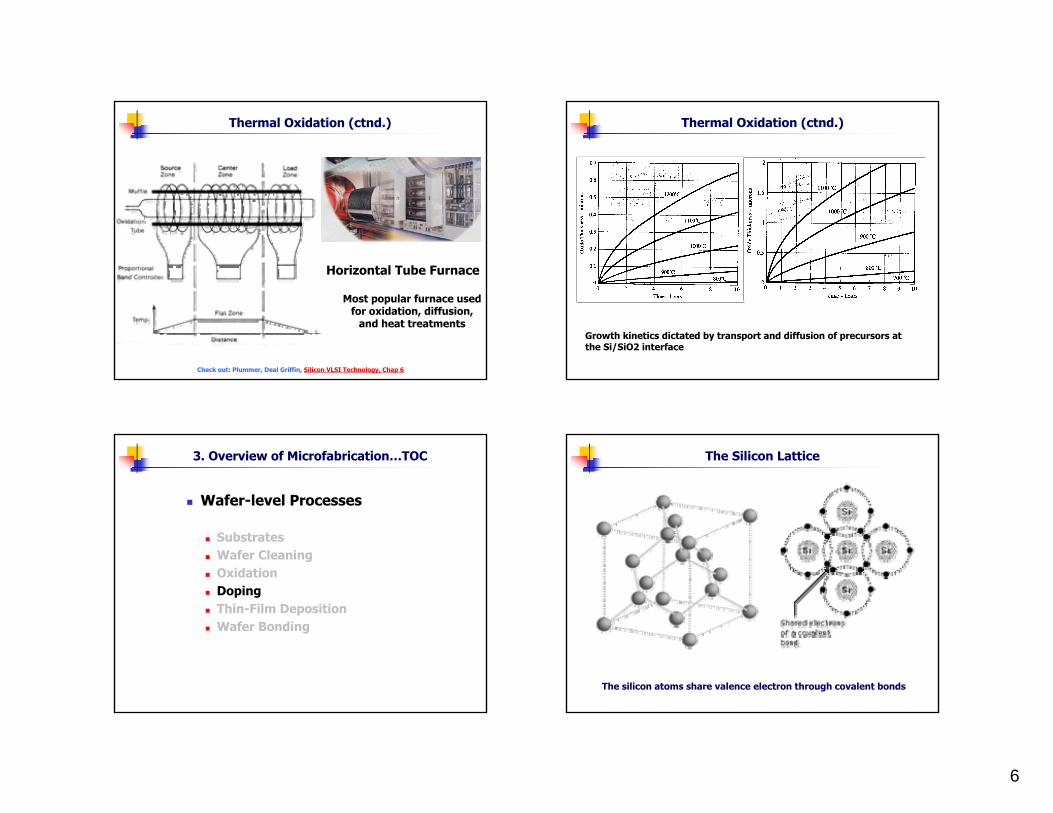
Thermal Oxidation (ctnd.)
Horizontal Tube Furnace
Most popular furnace used for oxidation, diffusion,
and heat treatments
Check out: Plummer, Deal Griffin, Silicon VLSI Technology, Chap 6
Thermal Oxidation (ctnd.)
Growth kinetics dictated by transport and diffusion of precursors at the Si/SiO2 interface
3. Overview of Microfabrication…TOC
Wafer-level Processes
SubstratesWafer CleaningOxidationDopingThin-Film DepositionWafer Bonding
The Silicon Lattice
The silicon atoms share valence electron through covalent bonds
7
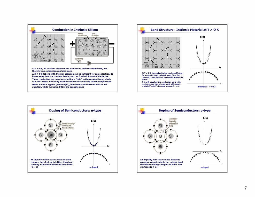
Conduction in Intrinsic Silicon
At T = 0 K, all covalent electrons are localized to their co-valent bond, and therefore no conduction can take place.At T > 0 K (above left), thermal agitation can be sufficient for some electrons to break away from the covalent bonds, and can freely drift around the latticeThese conduction electrons leave behind a "hole" in the covalent bond, which can also "move" by having nearby covalent electrons hop into the empty stateWhen a field is applied (above right), the conduction electrons drift in one direction, while the holes drift in the opposite ones
Band Structure : Intrinsic Material at T > O K
intrinsic (T > 0 K)
Ef
E(k)
At T > 0 K, thermal agitation can be sufficient for some electrons to break away from the covalent bonds, and can freely drift around the lattice.This will populate the conduction band with electrons, and the valence band with empty orbitals ("holes"), in equal amount (n = p)
Doping of Semiconductors: n-type
An impurity with extra valence electron releases this electron in lattice, therefore creating a surplus of electrons over holes (n > p) n-doped
E(k)
Ef
Doping of Semiconductors: p-type
An impurity with less valence electrons creates a vacant state in the valence band therefore creating a surplus of holes over electrons (p > n) p-doped
Ef
E(k)
8
Summary : Intrinsic vs Doped Material
n-doped p-dopedintrinsic
Ef
E(k) E(k)
Ef
Ef
E(k)
The n-doped material is rich in negatively charged conduction electrons
The p-doped material is rich in positively charged valence band holes
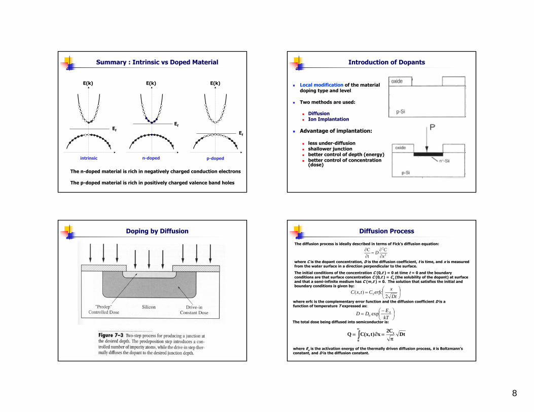
Introduction of Dopants
Local modification of the material doping type and level
Two methods are used:
Diffusion Ion Implantation
Advantage of implantation:
less under-diffusionshallower junctionbetter control of depth (energy)better control of concentration (dose)
Doping by Diffusion Diffusion Process
∫∞
π=∂=
0
s DtC2x)t,x(CQ
The diffusion process is ideally described in terms of Fick’s diffusion equation:
2
2
tC
xCD
∂∂
=∂∂
where C is the dopant concentration, D is the diffusion coefficient, t is time, and x is measured from the water surface in a direction perpendicular to the surface.
The initial conditions of the concentration C (0,t ) = 0 at time t = 0 and the boundary conditions are that surface concentration C (0,t ) = Cs (the solubility of the dopant) at surface and that a semi-infinite medium has C (∞,t ) = 0. The solution that satisfies the initial and boundary conditions is given by:
⎟⎠
⎞⎜⎝
⎛=DtxerfcCtxC S 2
),(
⎟⎠⎞
⎜⎝⎛ −=
kTEDD Aexp0
where erfc is the complementary error function and the diffusion coefficient D is a function of temperature T expressed as:
where Ea is the activation energy of the thermally driven diffusion process, k is Boltzmann’sconstant, and D is the diffusion constant.
The total dose being diffused into semiconductor is:

9
Diffusion Process (ctnd.) Diffusion Process (ctnd.)
Diffusion Process (ctnd.)
⎟⎠⎞
⎜⎝⎛ −=
kTEDD Aexp0
Numerical Example
Q: A p-type (boron) diffusion is performed in silicon as follows for 30 min at 900˚C. What is the deposited Q? Assume that the solid solubility is maintained at the surface (x=0)
Solution:According to figures above, the boron diffusion coefficient is:
at 900˚C:
The deposition is performed at 900˚C where the boron solid solubility from Table 7.4 is:
The dose introduced is then:
( )1216900
B scm1027.9273900k
5.3exp0.1D −−×=⎟⎟⎠
⎞⎜⎜⎝
⎛+
−=
320S cm102.1C −×=
( ) ( )( ) 2141620
S cm1075.160301027.9102.12DtC2Q −− ×=××π×
=π
=
10
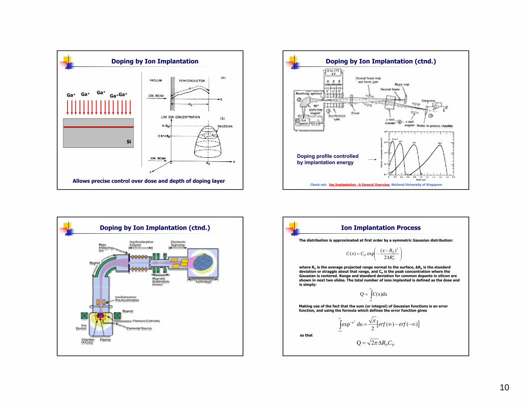
Doping by Ion Implantation
Si
Ga+ Ga+ Ga+Ga+Ga+
Allows precise control over dose and depth of doping layer
Doping profile controlled by implantation energy
Doping by Ion Implantation (ctnd.)
Check out: Ion Implantation : A General Overview, National University of Singapore
Doping by Ion Implantation (ctnd.) Ion Implantation Process
The distribution is approximated at first order by a symmetric Gaussian distribution:
⎟⎟⎠
⎞⎜⎜⎝
⎛Δ−
−= 2
2
2)(exp)(
P
PP R
RxCxC
where RP is the average projected range normal to the surface, ∆RP is the standard deviation or straggle about that range, and CP is the peak concentration where the Gaussian is centered. Range and standard deviation for common dopants in silicon are shown in next two slides. The total number of ions implanted is defined as the dose and is simply:
∫∞
∞
=-
C(x)dxQ
Making use of the fact that the sum (or integral) of Gaussian functions is an error function, and using the formula which defines the error function gives
[ ])()(2
exp2
−∞−∞=∫∞
∞−
− erferfduu π
so that
PPCRΔ= π2Q

11
Ion Implantation Process (ctnd.) Ion Implantation Process (ctnd.)
Ion Implantation Process (ctnd.) Numerical Example
Q: Arsenic is implanted into a lightly doped p-type Si substrate at an energy of 75 keV. The dose is 1 x 1014 cm-2. The Si substrate is tilted 7° with respect to the ion beam to make it appear amorphous. The implanted region is assumed to be rapidly annealed so that complete electrical activation is achieved. What is the peak electron concentration produced?
A: From above graphs, the range and standard deviation for 75 keVarsenic are
The peak concentration is:
Assuming all the dose is active, then the peak electron concentration is equal to the peak dopant concentration.
RP = 0.05μm ΔRP = 0.02μm
CP =Q
2π ΔRP=
1×10¹⁴
2π 0.02 ×10⁻⁴( )= 2 ×1019 cm−3
12
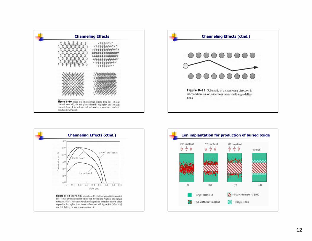
Channeling Effects Channeling Effects (ctnd.)
Channeling Effects (ctnd.) Ion implantation for production of buried oxide

13
Cross-section of SIMOX wafers SIMOX wafers for MEMS devices
3. Overview of Microfabrication…TOC
Wafer-level Processes
SubstratesWafer CleaningOxidationDopingThin-Film DepositionWafer Bonding
Electronics Materials
Typical IC materials include:
Thermal Oxides (covered previously)
Other Dielectric Materials
Polycrystalline silicon (Poly-Si)
Metals
14
Electronics Materials
Typical IC materials include:
Thermal Oxides (covered previously)
Other Dielectric Materials
Polycrystalline silicon (Poly-Si)
Metals
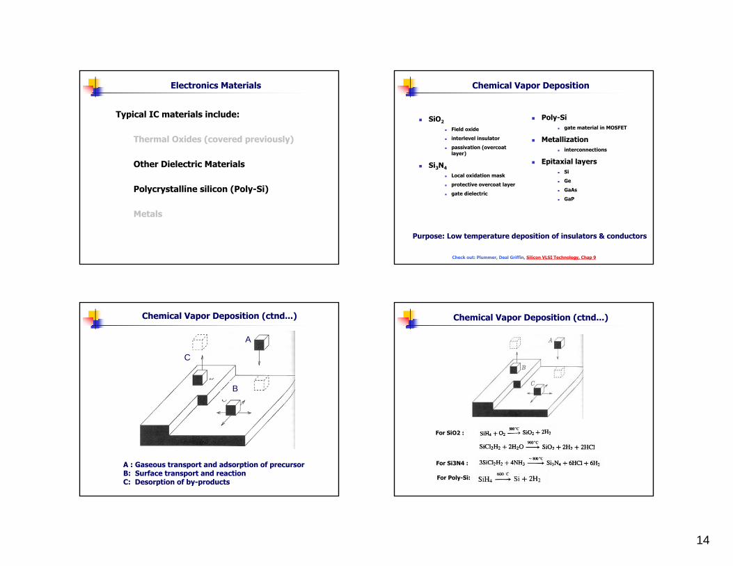
Chemical Vapor Deposition
SiO2
Field oxide
interlevel insulator
passivation (overcoat layer)
Si3N4
Local oxidation mask
protective overcoat layer
gate dielectric
Purpose: Low temperature deposition of insulators & conductors
Poly-Sigate material in MOSFET
Metallizationinterconnections
Epitaxial layersSi
Ge
GaAs
GaP
Check out: Plummer, Deal Griffin, Silicon VLSI Technology, Chap 9
Chemical Vapor Deposition (ctnd...)
A
B
C
A : Gaseous transport and adsorption of precursorB: Surface transport and reactionC: Desorption of by-products
Chemical Vapor Deposition (ctnd...)
For SiO2 :
For Si3N4 :
For Poly-Si:
15
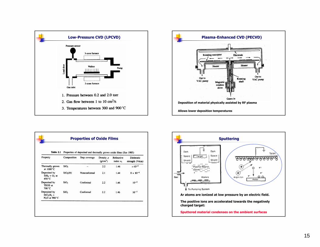
Low-Pressure CVD (LPCVD) Plasma-Enhanced CVD (PECVD)
Deposition of material physically assisted by RF plasma
Allows lower deposition temperatures
Properties of Oxide Films Sputtering
Ar atoms are ionized at low pressure by an electric field.
The positive ions are accelerated towards the negatively charged target:
Sputtered material condenses on the ambient surfaces

16
Electronics Materials
Typical IC materials include:
Thermal Oxides
Dielectric Materials
Polycrystalline silicon (Poly-Si)
Metals
Metallization
Purpose: interconnecting the devices to form a circuit
Use low resistance metal layers:
Aluminum alloys
Silicides
Copper
Important issues:
resistivity
electromigration
planarity
(Source: AMD)
Nine levels of metallization(with low-k dielectric and SiC-based barriers)
Copper introduced in 2001 by IBMLower resistance than AluminumLess interconnection delays on chipHigher clock frequencies possible
Check out: Plummer, Deal, Griffin, Silicon VLSI Technology, Chap 11
Metallization by Evaporation 3. Overview of Microfabrication…TOC
Wafer-level Processes
SubstratesWafer CleaningOxidationDopingThin-Film DepositionWafer Bonding
17
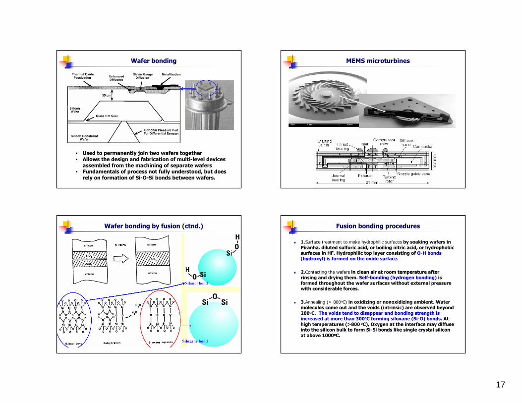
Wafer bonding
• Used to permanently join two wafers together• Allows the design and fabrication of multi-level devices
assembled from the machining of separate wafers• Fundamentals of process not fully understood, but does
rely on formation of Si-O-Si bonds between wafers.
MEMS microturbines
Wafer bonding by fusion (ctnd.) Fusion bonding procedures
1.Surface treatment to make hydrophilic surfaces by soaking wafers in Piranha, diluted sulfuric acid, or boiling nitric acid, or hydrophobic surfaces in HF. Hydrophilic top layer consisting of O-H bonds (hydroxyl) is formed on the oxide surface.
2.Contacting the wafers in clean air at room temperature after rinsing and drying them. Self-bonding (hydrogen bonding) is formed throughout the wafer surfaces without external pressure with considerable forces.
3.Annealing (> 800oC) in oxidizing or nonoxidizing ambient. Water molecules come out and the voids (intrinsic) are observed beyond 200oC. The voids tend to disappear and bonding strength is increased at more than 300oC forming siloxane (Si-O) bonds. At high temperatures (>800 oC), Oxygen at the interface may diffuse into the silicon bulk to form Si-Si bonds like single crystal silicon at above 1000oC.
18
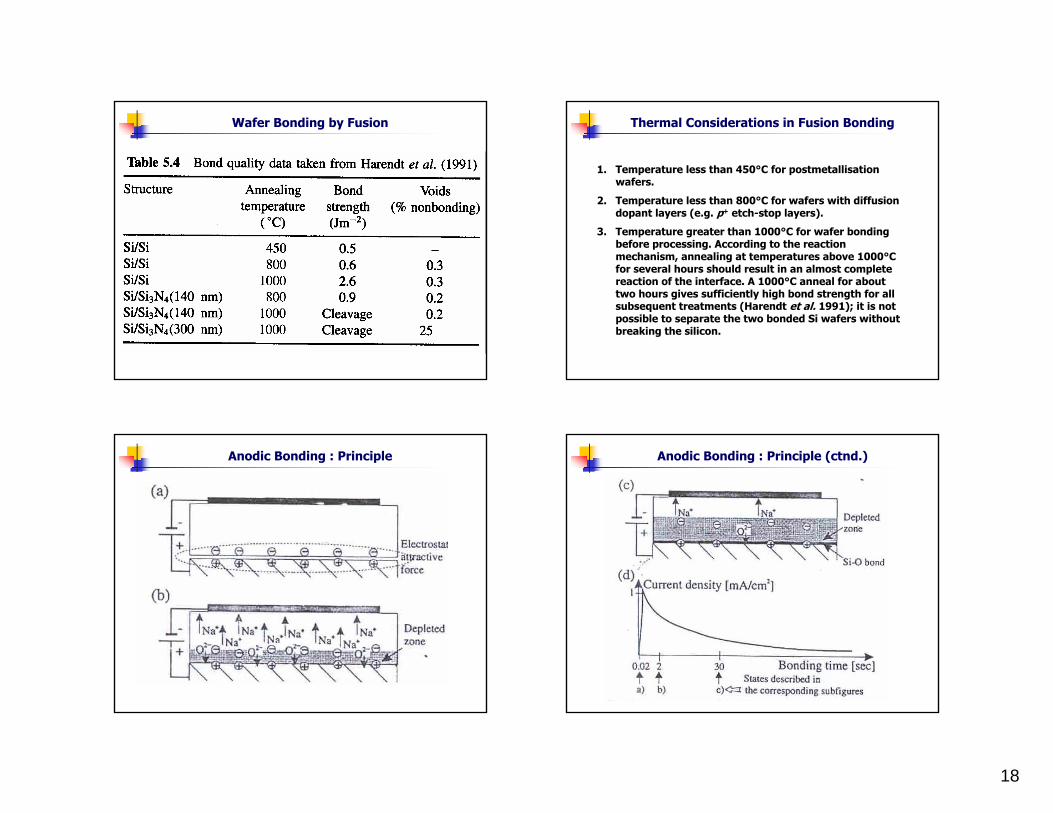
Wafer Bonding by Fusion Thermal Considerations in Fusion Bonding
1. Temperature less than 450°C for postmetallisationwafers.
2. Temperature less than 800°C for wafers with diffusion dopant layers (e.g. p+ etch-stop layers).
3. Temperature greater than 1000°C for wafer bonding before processing. According to the reaction mechanism, annealing at temperatures above 1000°C for several hours should result in an almost complete reaction of the interface. A 1000°C anneal for about two hours gives sufficiently high bond strength for all subsequent treatments (Harendt et al. 1991); it is not possible to separate the two bonded Si wafers without breaking the silicon.
Anodic Bonding : Principle Anodic Bonding : Principle (ctnd.)

19
Anodic Bonding : Principle (ctnd.)
General Principles: Due to the elevated temperature, the Na+ ions are mobile enough for the Pyrex to behave like a conductor. Hence, in the very first moment, most of the voltage applied to the silicon-Pyrex sandwich drops across a small gap of a few microns betweenthe two surfaces.
The high electric field in this area creates a strong electrostatic force, pulling the two surfaces together and thus forming an intimate contact.
In addition Na+ ions start drifting to the negative electrode, which is connected with glass, creating depletion zone adjacent to thesilicon, positive electrode.
During this charging process, the electric field is high enough to allow a drift of oxygen to the positive electrode (Si) reacting with silicon and creating Si-O bond.
Anodic Bonding Setup
Glass sputtered onto one of the silicon surfaces
Bonding take place at T ~300-400 C, at V = 50 - 1200 V (greatly varies depending on glass used for bonding)
Anodic Bonding : Procedure
Typical Variables: temperature, applied voltage, bonding load, voltage-applying time, bonding area, glass thickness. 300 – 400 oC, 700-1200V. (FYI: Temperature limit for IC processed Si substrates is about 450 oC)General conditions: Silicon + Pyrex 7740, 400 oC, and 1000V.Requirements:
Microroughness (Ra) < 1μm. Warp/bow < 5μmThe native or thermal oxide layer on the Si must be thinner than2000Å.
Benefits: Lower temperature process and popular and reliable processLess stringent requirement for the surface quality of the wafers.
Alternate Bonding Technique : Eutectic Bonding
One wafer coated with Au prior to bondingTemperature is raised until the Eutectic point is reachedAbove eutectic temperature, Au will diffuse into Si (and not other way aroundAn Au-Si eutectic alloy is then formed between the two wafersOther Si-metal alloys eutecic bonding also possible

20
IR Monitoring of Bonded Wafers
Quality of bonds is usually monitored using infrared absorption imaging
Worked Example : Floating Element Shear Sensor
(a) Angled view and (b) cross section of a floating sensor based on a rectangular plate with four tethers
Worked Example : Floating Element Shear Sensor
A better view of geometry of such device
SiSiO2
Si
Worked example : Floating Element Shear Sensor

21
Worked example : Floating Element Shear Sensor 3. Overview of Microfabrication…TOC
Pattern Transfer
Optical LithographyDesign RulesMask MakingWet EtchingDry-EtchingLift-OffPlanarization
3. Overview of Microfabrication…TOC
Pattern Transfer
Optical LithographyDesign RulesMask MakingWet EtchingDry-EtchingLift-OffPlanarization
Lithography
Masks
Photoresists
OxideSilicon

22
Elements of Photolithography Elements of Photolithography (ctnd.)
Lithography consists of patterning substrate by employing the interaction of beams of photons or particles with materials.
Photolithography is widely used in the integrated circuits (ICs) manufacturing.
The process of IC manufacturing consists of a series of 10-20 steps or more, called mask layerswhere layers of materials coated with resists are patterned then transferred onto the material layer.
Elements of photolithography (ctnd.)
A photolithography system consists of a light source, a mask, and a optical projection system.
Photoresists are radiation sensitive materials that usually consist of a photo-sensitive compound, a polymeric backbone, and a solvent.
Resists can be classified upon their solubility after exposure into: positive resists (solubility of exposed area increases) and negative resists(solubility of exposed area decreases).
Positive vs. Negative Photoresists
23
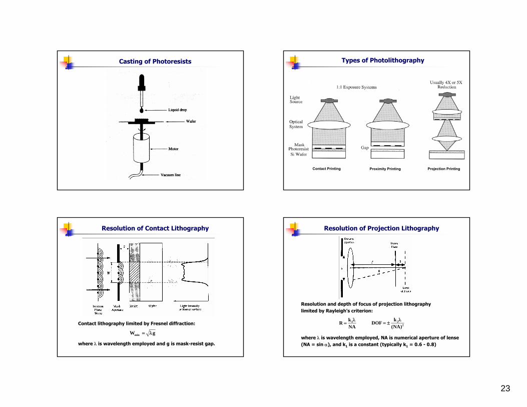
Casting of Photoresists Types of Photolithography
Contact Printing Proximity Printing Projection Printing
Resolution of Contact Lithography
gWmin λ=
Contact lithography limited by Fresnel diffraction:
where λ is wavelength employed and g is mask-resist gap.
Resolution of Projection Lithography
Resolution and depth of focus of projection lithography limited by Rayleigh's criterion:
where λ is wavelength employed, NA is numerical aperture of lense(NA = sin α), and k1 is a constant (typically k1 = 0.6 - 0.8)
NAkR 1λ= 2
2
)NA(kDOF λ
±=
24
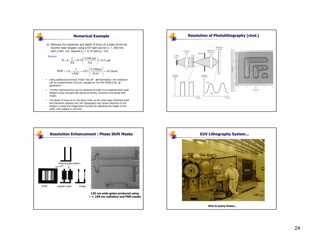
Numerical Example
μm31.00.6
μm248.075.01 =⎟⎠⎞
⎜⎝⎛==
NAkR λ
Q: Estimate the resolution and depth of focus of a state-of-the-art excimer laser stepper using a KrF light source (λ = 248 nm) with a NA= 0.6. Assume k1 = 0.75 and k2= 0.5.
Answer
mmNA
μμλ 34.0)6.0(
248.05.0)(
k DOF 222 ±=⎥⎦
⎤⎢⎣
⎡±=±=
• Using additional technical “tricks” like off- axis illumination, the resolution can be pushed below 0.25 μm, suitable for the SIA NTRS 0.25- μm generation.
• Further improvements can be obtained through more sophisticated mask designs using concepts like optical proximity correction and phase shift masks.
• The depth of focus is on the same order as the resist layer thickness itself and therefore requires very flat topography and careful attention in the stepper to keep the image plane focused by adjusting the height of the wafer with respect to the lens.
Resolution of Photolithography (ctnd.)
Resolution Enhancement : Phase Shift Masks
PSM regular mask image
Original gate pattern
120 nm wide gates produced using λ = 248 nm radiation and PSM masks
EUV Lithography System...
One in every home...
25
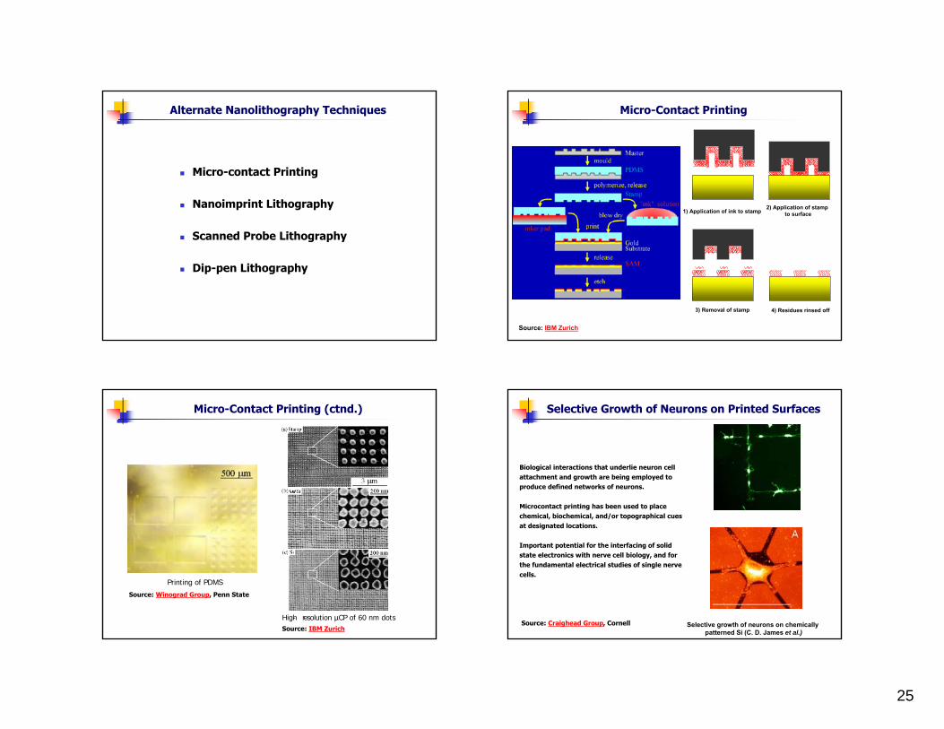
Alternate Nanolithography Techniques
Micro-contact Printing
Nanoimprint Lithography
Scanned Probe Lithography
Dip-pen Lithography
Micro-Contact Printing
1) Application of ink to stamp 2) Application of stamp to surface
3) Removal of stamp 4) Residues rinsed off
Source: IBM Zurich
Micro-Contact Printing (ctnd.)
High- resolution µCP of 60 nm dots Source: IBM Zurich
Printing of PDMS
Source: Winograd Group, Penn State
Biological interactions that underlie neuron cell attachment and growth are being employed to produce defined networks of neurons.
Microcontact printing has been used to place chemical, biochemical, and/or topographical cues at designated locations.
Important potential for the interfacing of solid state electronics with nerve cell biology, and for the fundamental electrical studies of single nerve cells.
Selective growth of neurons on chemically patterned Si (C. D. James et al.)
Selective Growth of Neurons on Printed Surfaces
Source: Craighead Group, Cornell

26
Alternate Nanolithography Techniques
Micro-contact Printing
Nanoimprint Lithography
Scanned Probe Lithography
Dip-pen Lithography
Nanoimprint Lithography
Consists of pressing a mold onto the resist above its glass transition temperature Tg
More ? Check out S. Y. Chou, Princeton
NIL Master
SiO2 pillars with 10 nm diameter, 40 nm spacing, and 60 nm height fabricated by e-beam lithography.
Master can be used tens of times without degradation
NIL Pattern in PMMA
Mask is pressed into 80 nm thick layer of PMMA on Si substrate at 175° C (Tg=105 ° C), P= 4.4 MPa.
PMMA conforms to master patterng, resulting in ~10 nm range holes
27
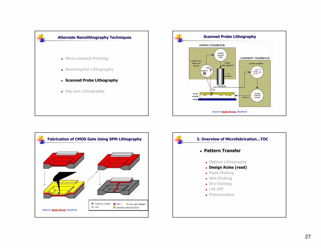
Alternate Nanolithography Techniques
Micro-contact Printing
Nanoimprint Lithography
Scanned Probe Lithography
Dip-pen Lithography
Source: Quate Group, Stanford
Scanned Probe Lithography
Fabrication of CMOS Gate Using SPM Lithography
Source: Quate Group, Stanford
3. Overview of Microfabrication…TOC
Pattern Transfer
Optical LithographyDesign Rules (read)Mask MakingWet EtchingDry-EtchingLift-OffPlanarization

28
3. Overview of Microfabrication…TOC
Pattern Transfer
Optical LithographyDesign RulesMask Making (read)Wet EtchingDry-EtchingLift-OffPlanarization
3. Overview of Microfabrication…TOC
Pattern Transfer
Optical LithographyDesign RulesMask MakingWet EtchingDry-EtchingLift-OffPlanarization
• Selective removal of material as defined by photolithography
Remove photoresist
Etch
Need for Etching Processes Isotropic vs. Anisotropic Etching

29
Selectivity of Etch Process Isotropic vs anisotropic etching : etching bias
Degree of anisotropy Wet Etching of Si
Etching of Si :
222 HSiHSi +⎯→⎯+ ++
)()( gasSiClabsorbedSiCl nn ⎯→⎯

30
Anisotropic etchants in silicon
w = w0 -2h coth (55o)
Anisotropic etchants in silicon (ctnd.)
KOH etch of Si Example MEMS Velcro

31
Example : MEMS Velcro (ctnd.) Wet Etching of Other Materials
Need for etch-stopping layers Need for etch-stopping layers (ctnd.)

32
Doping-selective etching Doping-selective etching (ctnd.)
Disadvantage: requires high-dopant concentration to achieve good selectivity
Electrochemical etching
1. Injection of holes into the semiconductor to raise it to a higher oxidation state Si+
2. Attachment of negatively charged hydroxyl groups, OH-, to the positively charged Si
3. Reaction of the hydrated silicon with the complexingagent in the solution
4. Dissolution of the reaction products into the etchant solution
Steps
Electrochemical etching ctnd.)
Plot of electrochemical current density against voltage for silicon doped to different resistivities
33
Electrochemical etch stop (ctnd.)
Current-voltage characteristics of n-Si and p-Si in KOH. No current flows at the OCP and the current stops above the passivating potential
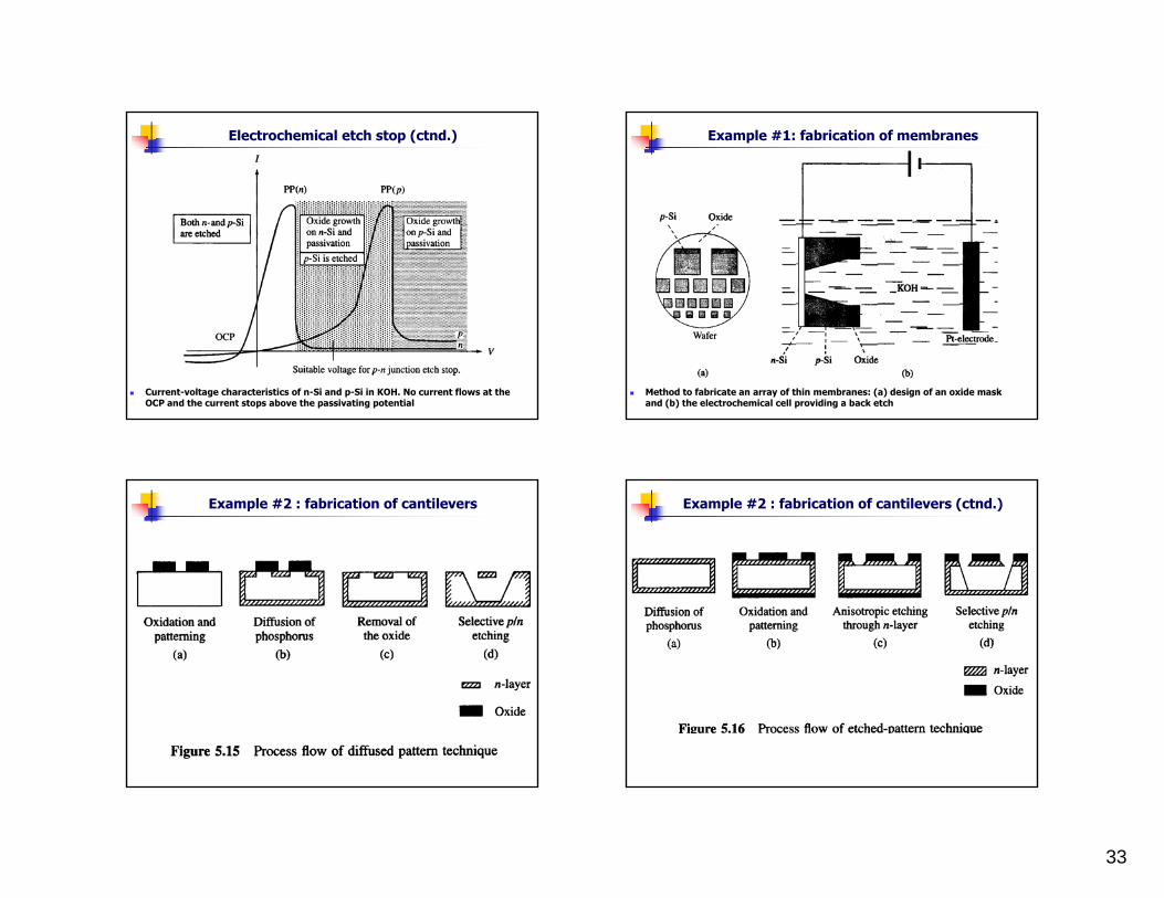
Example #1: fabrication of membranes
Method to fabricate an array of thin membranes: (a) design of an oxide mask and (b) the electrochemical cell providing a back etch
Example #2 : fabrication of cantilevers Example #2 : fabrication of cantilevers (ctnd.)

34
3. Overview of Microfabrication…TOC
Pattern Transfer
Optical LithographyDesign RulesMask MakingWet EtchingDry-EtchingLift-OffPlanarization
Dry Etching Methods
Dry etching required for small feature size:
Anisotropic
High aspect ratios
Types:
Reactive lon etching (right)
Sputtering
Ion beam milling
Check out: Plummer, Deal Griffin, Silicon VLSI Technology, Chap 10
Plasma Etching Plasma Induced Etching Processes
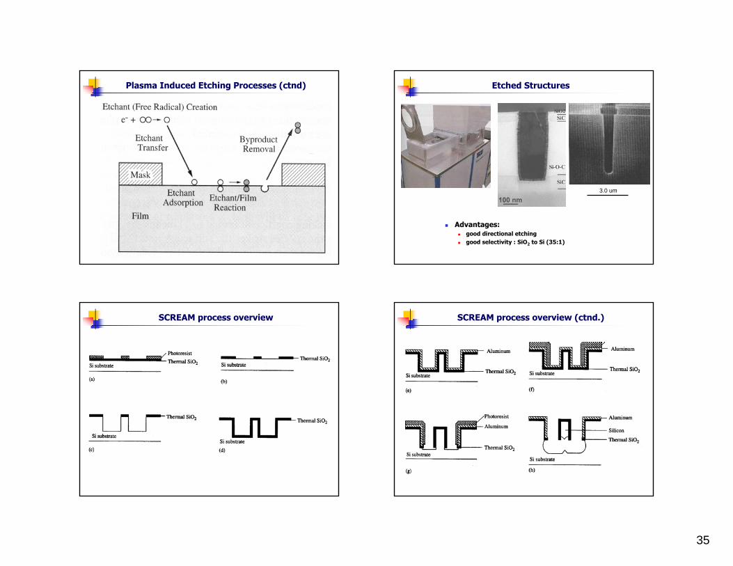
35
Plasma Induced Etching Processes (ctnd) Etched Structures
Advantages:good directional etchinggood selectivity : SiO2 to Si (35:1)
3.0 um
SCREAM process overview SCREAM process overview (ctnd.)
36
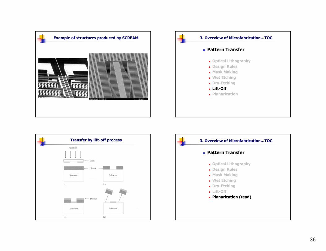
Example of structures produced by SCREAM 3. Overview of Microfabrication…TOC
Pattern Transfer
Optical LithographyDesign RulesMask MakingWet EtchingDry-EtchingLift-OffPlanarization
Transfer by lift-off process 3. Overview of Microfabrication…TOC
Pattern Transfer
Optical LithographyDesign RulesMask MakingWet EtchingDry-EtchingLift-OffPlanarization (read)