3 program sequencer - smdsmd.hu/data/analog/dsp/21xx/adsp-2191 hardware reference...adsp-219x/2191...
TRANSCRIPT

ADSP-219x/2191 DSP Hardware Reference 3-1
3 PROGRAM SEQUENCERFigure 3-0.
Table 3-0.
Listing 3-0.
OverviewThe DSP’s program sequencer controls program flow, constantly provid-ing the address of the next instruction to be executed by other parts of the DSP. Program flow in the DSP is mostly linear with the processor execut-ing program instructions sequentially. This linear flow varies occasionally when the program uses non-sequential program structures, such as those illustrated in Figure 3-1. Non-sequential structures direct the DSP to exe-cute an instruction that is not at the next sequential address. These structures include:
• Loops. One sequence of instructions executes several times with near-zero overhead.
• Subroutines. The processor temporarily interrupts sequential flow to execute instructions from another part of program memory.
• Jumps. Program flow transfers permanently to another part of pro-gram memory.
• Interrupts. Subroutines in which a runtime event triggers the exe-cution of the routine.
• Idle. An instruction that causes the processor to cease operations, holding its current state until an interrupt occurs. Then, the proces-sor services the interrupt and continues normal execution.

Overview
3-2 ADSP-219x/2191 DSP Hardware Reference
The sequencer manages execution of these program structures by selecting the address of the next instruction to execute. As part of this process, the sequencer handles the following tasks:
• Increments the fetch address
• Maintains stacks
• Evaluates conditions
• Decrements the loop counter
Figure 3-1. Program Flow Variations
N
N+1
N+2
N+3
N+4
N+5
ADDRESS:
INSTRUCTION
INSTRUCTION
INSTRUCTION
INSTRUCTION
INSTRUCTION
INSTRUCTION
LINEAR FLOW
INSTRUCTION
INSTRUCTION
INSTRUCTION
INSTRUCTION
INSTRUCTION
DO UNTIL
LOOP
N TIMES
INSTRUCTION
INSTRUCTION
INSTRUCTION
INSTRUCTION
INSTRUCTION
JUMP
JUMP
INSTRUCTION
INSTRUCTION
…
INSTRUCTION
CALL
SUBROUTINE
INSTRUCTION
RTS
INSTRUCTION
INSTRUCTION
…
INSTRUCTION
INSTRUCTION
INSTRUCTION
RTI
INSTRUCTION
INTERRUPT
IRQ
VECTOR
INSTRUCTION
INSTRUCTION
INSTRUCTION
INSTRUCTION
IDLE
INSTRUCTION
INSTRUCTION
IDLE
WAITINGFOR IRQ
INSTRUCTION
INSTRUCTION
ADSP-219x/2191 DSP Hardware Reference 3-3
Program Sequencer
• Calculates new addresses
• Maintains an instruction cache
• Handles interrupts
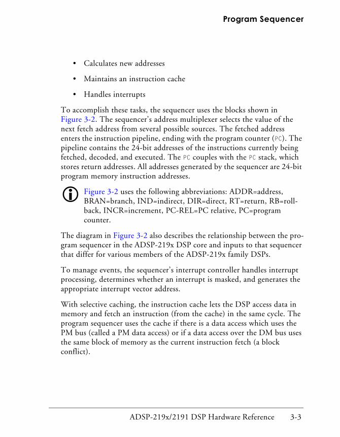
To accomplish these tasks, the sequencer uses the blocks shown in Figure 3-2. The sequencer’s address multiplexer selects the value of the next fetch address from several possible sources. The fetched address enters the instruction pipeline, ending with the program counter (PC). The pipeline contains the 24-bit addresses of the instructions currently being fetched, decoded, and executed. The PC couples with the PC stack, which stores return addresses. All addresses generated by the sequencer are 24-bit program memory instruction addresses.
� Figure 3-2 uses the following abbreviations: ADDR=address, BRAN=branch, IND=indirect, DIR=direct, RT=return, RB=roll-back, INCR=increment, PC-REL=PC relative, PC=program counter.
The diagram in Figure 3-2 also describes the relationship between the pro-gram sequencer in the ADSP-219x DSP core and inputs to that sequencer that differ for various members of the ADSP-219x family DSPs.
To manage events, the sequencer’s interrupt controller handles interrupt processing, determines whether an interrupt is masked, and generates the appropriate interrupt vector address.
With selective caching, the instruction cache lets the DSP access data in memory and fetch an instruction (from the cache) in the same cycle. The program sequencer uses the cache if there is a data access which uses the PM bus (called a PM data access) or if a data access over the DM bus uses the same block of memory as the current instruction fetch (a block conflict).

Overview
3-4 ADSP-219x/2191 DSP Hardware Reference
Figure 3-2. Program Sequencer Block Diagram
INTERRUPT CONTROLLER
INTERRUPTS
PREFETCH ADDRESS (PA)
FETCH ADDRESS (FA)
ADDRESS DECODE (AD)
INSTRUCTION DECODE (ID)
EXECUTE (PC)
INSTRUCTION PIPELINE
RBADDR
INCRADDR
PC-RELBRAN
DIRBRAN
INDBRAN
LOOPADDR
RTADDR
PC STACKLOOP STACK
LOOK AHEAD ADDRESS (LA)
+1
+
INSTR CACHE
INSTR LATCH
STATUS &CONDITION
LOOP STATUS
ARITHMETIC STATUS
COUNTER EXPIRED (CE)
LOOP & BRANCHCONTROL
ADSP-219XDSP SPECIFIC
ADSP-219X DSP CORE(COMMON TO ADSP-219X FAMILY)
DMA CONTROLLER
DMA REQUESTS
PROGRAMMABLEFLAGS
PM DATA BUS
PM ADDRESS BUS
VECTORADDR
PC STATUS
STACKADDRESS
ADDRESSFROM
DAGS

ADSP-219x/2191 DSP Hardware Reference 3-5
Program Sequencer
In addition to providing data addresses, the Data Address Generators (DAGs) provide instruction addresses for the sequencer’s indirect branches.
The sequencer evaluates conditional instructions and loop termination conditions using information from the status registers. The loop stacks support nested loops. The status stack stores status registers for imple-menting interrupt service routines.
Table 3-1 and Table 3-2 list the registers within and related to the pro-gram sequencer. All registers in the program sequencer are Register Group 1 (Reg1), 2 (Reg2), or 3 (Reg3) registers, so they are accessible to other data (Dreg) registers and to memory. All the sequencer’s registers are directly readable and writable, except for the PC. Manual pushing or pop-ping the PC stack is done using explicit instructions and the PC stack page (STACKP) and address (STACKA) registers, which are readable and writable. Pushing or popping the loop stacks and status stack also requires explicit instructions. For information on using these stacks, see “Stacks and Sequencing” on page 3-34.
A set of system control registers configures or provides input to the sequencer. These registers include ASTAT, MSTAT, CCODE, IMASK, IRPTL, and ICNTL. Writes to some of these registers do not take effect on the next cycle. For example, after a write to the MSTAT register to enable ALU satu-ration mode, the change does not take effect until one cycles after the write. With the lists of sequencer and system registers, Table 3-1 and Table 3-2 summarize the number of extra cycles (latency) for a write to take effect (effect latency) and for a new value to appear in the register (read latency). A “0” indicates that the write takes effect or appears in the register on the next cycle after the write instruction is executed, and a “1” indicates one extra cycle.

Overview
3-6 ADSP-219x/2191 DSP Hardware Reference
Table 3-1. Program Sequencer Register Effect Latencies
Register Contents Bits Effect Latency
CNTR loop count loaded on next Do/Until loop 16 11
IJPG Jump Page (upper eight bits of address) 8 1
IOPG I/O Page (upper eight bits of address) 8 1
DMPG1 DAG1 Page (upper eight bits of address) 8 1
DMPG2 DAG2 Page (upper eight bits of address) 8 1
1 CNTR has a one-cycle latency before an If Not CE instruction, but has zero latency otherwise.
Table 3-2. System Register Effect Latencies
Register Contents Bits Effect Latency
ASTAT Arithmetic status 9 1
MSTAT Mode status 7 01
SSTAT System status 8 n/a
CCODE Condition Code 16 1
IRPTL Interrupt latch 16 1
IMASK Interrupt mask 16 1
ICNTL Interrupt control 16 1
CACTL Cache control 3 52
1 Changing MSTAT bits with the Ena or Dis mode instruction has a 0 effect latency; when writing to MSTAT or performing a Pop Sts, the effect latencies vary based on the altered bits.
2 Except for the CFZ bit, which has an effect latency of four cycles.

ADSP-219x/2191 DSP Hardware Reference 3-7
Program Sequencer
The following sections in this chapter explain how to use each of the func-tional blocks in Figure 3-2:
• “Instruction Pipeline” on page 3-7
• “Instruction Cache” on page 3-9
• “Branches and Sequencing” on page 3-13
• “Loops and Sequencing” on page 3-21
• “Interrupts and Sequencing” on page 3-25
• “Stacks and Sequencing” on page 3-34
• “Conditional Sequencing” on page 3-39
• “Sequencer Instruction Summary” on page 3-41
Instruction PipelineThe program sequencer determines the next instruction address by exam-ining both the current instruction being executed and the current state of the processor. If no conditions require otherwise, the DSP executes instructions from program memory in sequential order by incrementing the look-ahead address. Using its instruction pipeline, the DSP processes instructions in six clock cycles:
• Look-Ahead Address (LA). The DSP determines the source for the instruction from inputs to the look-ahead address multiplexer.
• Prefetch Address (PA) and Fetch Address (FA). The DSP reads the instruction from either the on-chip instruction cache or from pro-gram memory.

Instruction Pipeline
3-8 ADSP-219x/2191 DSP Hardware Reference
• Address Decode (AD) and Instruction Decode (ID). The DSP decodes the instruction, generating conditions that control instruc-tion execution.
• Execute (PC). The DSP executes the instruction; the operations specified by the instruction complete in a single cycle.
These cycles overlap in the pipeline, as shown in Table 3-3. In sequential program flow, when one instruction is being fetched, the instruction fetched three cycles previously is being executed. With few exceptions, sequential program flow has a throughput of one instruction per cycle. The exceptions are the two-cycle instructions: 16- or 24-bit immediate data write to memory with indirect addressing, long jump (Ljump), and long call (Lcall).
Table 3-3. Pipelined Execution Cycles
Cycles LA PA FA AD ID PC
1 0x08 �
2 0x09 � 0x08 �
3 0x0A � 0x09 � 0x08 �
4 0x0B � 0x0A � 0x09 � 0x08 �
5 0x0C � 0x0B � 0x0A � 0x09 � 0x08 �
6 0x0D � 0x0C � 0x0B � 0x0A � 0x09 � 0x08
7 0x0E � 0x0D � 0x0C � 0x0B � 0x0A � 0x09
8 0x0F 0x0E 0x0D 0x0C 0x0B 0x0A
Look Ahead Address (LA). Prefetch Address (PA). Fetch Address (FA). Address Decode (AD). Instruction Decode (ID). Execute (PC).

ADSP-219x/2191 DSP Hardware Reference 3-9
Program Sequencer
Any non-sequential program flow can potentially decrease the DSP’s instruction throughput. Non-sequential program operations include:
• Data accesses that conflict with instruction fetches
• Jumps
• Subroutine calls and returns
• Interrupts and return
• Loops (of less than five instructions)
Instruction CacheUsually, the sequencer fetches an instruction from memory on each cycle. Occasionally, bus constraints prevent some of the data and instructions from being fetched in a single cycle. To alleviate these data flow con-straints, the DSP has an instruction cache, which appears in Figure 3-3.
When the DSP executes an instruction that requires data access over the PM data bus, there is a bus conflict because the sequencer uses the PM data bus for fetching instructions.
When a data transfer over the DM bus accesses the same memory block from which the DSP is fetching an instruction, there is a block conflict because only one bus can access a block at a time.
To avoid bus and block conflicts, the DSP caches these instructions, reducing delays. Except for enabling or disabling the cache, its operation requires no intervention. For more information, see “Using the Cache” on page 3-11 and “Optimizing Cache Usage” on page 3-12.
The first time the DSP encounters a fetch conflict, the DSP must wait to fetch the instruction on the following cycle, causing a delay. The DSP automatically writes the fetched instruction to the cache to prevent the same delay from happening again.

Instruction Cache
3-10 ADSP-219x/2191 DSP Hardware Reference
The sequencer checks the instruction cache on every PM data access or block conflict. If the needed instruction is in the cache, the instruction fetch from the cache happens in parallel with the program memory data access, without incurring a delay.
Because of the six-stage instruction pipeline, as the DSP executes an instruction (at address n) that requires a PM data access or block conflict, this execution creates a conflict with the instruction fetch (at address n+3), assuming sequential execution. The cache stores the fetched instruc-tion (n+3), not the instruction requiring the data access.
If the instruction needed to avoid a conflict is in the cache, the cache pro-vides the instruction while the data access is performed. If the needed instruction is not in the cache, the instruction fetch from memory takes place in the cycle following the data access, incurring one cycle of over-head. If the cache is enabled and not frozen, the fetched instruction is loaded into the cache, so that it is available the next time the same conflict occurs.
Figure 3-3 shows a block diagram of the instruction cache. The cache holds 64 instruction-address pairs. These pairs (or cache entries) are arranged into 32 (31-0) cache sets according to the instruction address’ five least significant bits (4-0). The two entries in each set (entry 0 and entry 1) have a valid bit, indicating whether the entry contains a valid instruction. The least recently used (LRU) bit for each set indicates which entry was not used last (0=entry 0, and 1=entry 1).
The cache places instructions in entries according to the five LSBs of the instruction’s address. When the sequencer checks for an instruction to fetch from the cache, it uses the five address LSBs as an index to a cache set. Within that set, the sequencer checks the addresses and valid bits of the two entries, looking for the needed instruction. If the cache contains the instruction, the sequencer uses the entry and updates the LRU bit to indicate the entry did not contain the needed instruction.

ADSP-219x/2191 DSP Hardware Reference 3-11
Program Sequencer
When the cache does not contain a needed instruction, the cache loads a new instruction and its address, placing these in the least recently used entry of the appropriate cache set and toggling the LRU bit.
Using the CacheAfter a DSP reset, the cache starts cleared (containing no instructions), unfrozen, and enabled. From then on, the CACTL register controls the
Figure 3-3. Instruction Cache Architecture
INSTRUCTIONS
SET 0
SET 1
SET 2
SET 29
SET 30
SET 31
ADDRESSESBITS (23-5)
LRUBIT
VALIDBIT
ENTRY 0
ENTRY 0
ENTRY 0
ENTRY 1
ENTRY 1
ENTRY 1
ENTRY 0
ENTRY 0
ENTRY 0
ENTRY 1
ENTRY 1
ENTRY 1
ADDRESSESBITS (4-0)
00000
00001
00010
11101
11110
11111

Instruction Cache
3-12 ADSP-219x/2191 DSP Hardware Reference
operating mode of the instruction cache. Figure A-6 on page A-22 lists all the bits in CACTL. The following bits in CACTL control cache modes:
• Cache DM bus access Enable. Bit 5 (CDE) directs the sequencer to cache conflicting DM bus accesses (if 1) or not to cache conflicting DM bus accesses (if 0).
• Cache Freeze. Bit 6 (CFZ) directs the sequencer to freeze the contents of the cache (if 1) or let new entries displace the entries in the cache (if 0).
• Cache PM bus access Enable. Bit 7 (CPE) directs the sequencer to cache conflicting PM bus accesses (if 1) or not to cache conflicting PM bus accesses (if 0).
� When program memory changes, programs need to resynchronize the instruction cache with program memory using the Flush Cache instruction. This instruction flushes the instruction cache, invali-dating all instructions currently cached, so the next instruction fetch results in a memory access.
Optimizing Cache UsageUsually, cache operation is efficient and requires no intervention, but cer-tain ordering of instructions can work against the cache’s architecture and can degrade cache efficiency. When the order of PM bus data accesses or block conflicts and instruction fetches continuously displaces cache entries and loads new entries, the cache is not being efficient. Rearranging the order of these instructions remedies this inefficiency.
An example of code that works against cache efficiency appears in Table 3-4 on page 3-14. The program memory data access at address 0x0100 in the loop, Outer, causes the cache to load the instruction at 0x0103 (into set 19). Each time the program calls the subroutine, Inner, the program memory data accesses at 0x0300 and 0x500 displace the instruction at 0x0103 by loading the instructions at 0x0303 and 0x0503

ADSP-219x/2191 DSP Hardware Reference 3-13
Program Sequencer
(also into set 19). If the program only calls the Inner subroutine rarely during the Outer loop execution, the repeated cache loads do not greatly influence performance. If the program frequently calls the subroutine while in the loop, the cache inefficiency has a noticeable effect on perfor-mance. To improve cache efficiency on this code (if for instance, execution of the Outer loop is time-critical), it would be good to rearrange the order of some instructions. Moving the subroutine call up one loca-tion (starting at 0x02FE) would work here, because with that order the two cached instructions end up in cache set 18 instead of set 19.
� Because the least significant five address bits determine which cache set stores an instruction, instructions in the same cache set are mul-tiples of 64 address locations apart. As demonstrated in the optimi-zation example, it is a rare combination of instruction sequences that can lead to “cache thrashing”—iterative swapping of cache entries.
Branches and SequencingOne of the types of non-sequential program flow that the sequencer sup-ports is branching. A branch occurs when a Jump or Call/return instruction begins execution at a new location, other than the next sequential address. For descriptions on how to use the Jump and Call/return instructions, see the ADSP-219x DSP Instruction Set Refer-ence. Briefly, these instructions operate as follows:
• A Jump or a Call/return instruction transfers program flow to another memory location. The difference between a Jump and a Call is that a Call automatically pushes the return address (the next

Branches and Sequencing
3-14 ADSP-219x/2191 DSP Hardware Reference
sequential address after the Call instruction) onto the PC stack. This push makes the address available for the Call instruction’s matching return instruction, allowing easy return from the subroutine.
• A return instruction causes the sequencer to fetch the instruction at the return address, which is stored at the top of the PC stack. The two types of return instructions are return from subroutine (Rts) and return from interrupt (Rti). While the return from subroutine (Rts) only pops the return address off the PC stack, the return from interrupt (Rti) pops the return address and pops the status stack.
Table 3-4. Cache-Inefficient Code
Address Instruction
0x00FE CNTR=1024;
0x00FF Do Outer Until CE;
0x0100 AX0=DM(I0+=M0), PM(I4+=M4)=AY0;
...
0x0103 If EQ Call Inner;
0x0104 AR=AX1 + AY1;
0x0105 MR=MX0*MY0 (SS);
0x0106 Outer: SR=MX1*MY1(SS);
0x0107 PM(I7+=M7)=SR1;
...
0x02FF Inner: SR0=AY0;
0x0300 AY0=PM(I5+=M5);
...
0x0500 PM(I5+=M5)=AY1;
...
0x05FF Rts;

ADSP-219x/2191 DSP Hardware Reference 3-15
Program Sequencer
There are a number of parameters that programs can specify for branches:
• Jump and Call/return instructions can be conditional. The program sequencer can evaluate status conditions to decide whether to exe-cute a branch. If no condition is specified, the branch is always taken. For more information on these conditions, see “Conditional Sequencing” on page 3-39.
• Jump and Call/return instructions can be immediate or delayed. Because of the instructions pipeline, an immediate branch incurs four lost (overhead) cycles. A delayed branch incurs two cycles of overhead. For more information, see “Delayed Branches” on page 3-16.
• Jump and Call/return instructions can be used within Do/Until counter (CE) or infinite (Forever) loops, but a Jump or Call instruc-tion may not be the last instruction in the loop. For information, see “Restrictions on Ending Loops” on page 3-24.
The sequencer block diagram in Figure 3-2 on page 3-4 shows that branches can be direct or indirect. The difference is that the sequencer generates the address for a direct branch, and the PM data address genera-tor (DAG2) produces the address for an indirect branch.
Direct branches are Jump or Call/return instructions that use an abso-lute—not changing at runtime—address (such as a program label) or use a PC-relative 16-bit address. To branch farther, the Ljump or Lcall instruc-tions use a 24-bit address. Some instruction examples that cause a direct branch are:
Jump fft1024; {where fft1024 is an address label}Call 10; {where 10 a PC-relative address}
Indirect branches are Jump or Call/return instructions that use a dynamic—changes at runtime—address that comes from the PM data address generator. For more information on the data address generator,

Branches and Sequencing
3-16 ADSP-219x/2191 DSP Hardware Reference
see “DAG Operations” on page 4-8. Some instruction examples that cause an indirect branch are:
Jump (I6); {where (i6) is a DAG2 register}Call (I7); {where (i7) is a DAG2 register}
Indirect Jump Page (IJPG) RegisterThe IJPG register provides the upper eight address bits for indirect Jump and Call instructions. When performing an indirect branch, the sequencer gets the lower 16 bits of the branch address from the I register specified in the Jump or Call instruction and uses the IJPG register to com-plete the address.
At power up, the DSP initializes the IJPG register to 0x0. Initializing the page register only is necessary when the instruction is located on a page other than the current page.
� Changing the contents of the sequencer page register is not auto-matic and requires explicit programming.
Conditional BranchesThe sequencer supports conditional branches. These are Jump or Call/return instructions whose execution is based on testing an If condi-tion. For more information on condition types in If condition instructions, see “Conditional Sequencing” on page 3-39.
Delayed BranchesThe instruction pipeline influences how the sequencer handles branches. For immediate branches—Jump and Call/return instructions not specified as delayed branches (DB), four instruction cycles are lost (Nops) as the pipe-line empties and refills with instructions from the new branch.

ADSP-219x/2191 DSP Hardware Reference 3-17
Program Sequencer
As shown in Table 3-5 and Table 3-6, the DSP does not execute the four instructions after the branch, which are in the fetch and decode stages. For a Call, the next instruction (the instruction after the Call) is the return address. During the four lost (no-operation) cycles, the pipeline fetches and decodes the first instruction at the branch address.
For delayed branches—Jump and Call/return instructions with the delayed branches (DB) modifier, only two instruction cycles are lost in the pipeline, because the DSP executes the two instructions after the branch while the pipeline fills with instructions from the new branch.
Table 3-5. Pipelined Execution Cycles for Immediate Branch (Jump/Call)
Cycles LA PA FA AD ID PC
1 j n+4→nop1 n+3→nop1 n+2→nop1 n+1→nop1 n
2 j+1 j n+4→nop1 n+3→nop1 n+2→nop1 Nop2
3 j+2 j+1 j n+4→nop1 n+3→nop1 Nop
4 j+3 j+2 j+1 j n+4→nop1 Nop
5 j+4 j+3 j+2 j+1 j Nop
6 j+5 j+4 j+3 j+2 j+1 j
Note that n is the branching instruction, and j is the instruction branch address. 1. n+1, n+2, n+3, and n+4 are suppressed.2. For call, return address (n+1) is pushed on the PC stack.

Branches and Sequencing
3-18 ADSP-219x/2191 DSP Hardware Reference
Table 3-6. Pipelined Execution Cycles for Immediate Branch (Return)
Cycles LA PA FA AD ID PC
1 r n+4→nop1 n+3→nop1 n+2→nop1 n+1→nop1 n
2 r+1 r n+4→nop1 n+3→nop1 n+2→nop1 Nop2
3 r+2 r+1 r n+4→nop1 n+3→nop1 Nop
4 r+3 r+2 r+1 r n+4→nop1 Nop
5 r+4 r+3 r+2 r+1 r Nop
6 r+5 r+4 r+3 r+2 r+1 r
Note that n is the branching instruction, and r is the instruction branch address. 1. n+1, n+2, n+3, and n+4 are suppressed.2. r (n+1 in Table 3-5) the return address is popped from PC stack.

ADSP-219x/2191 DSP Hardware Reference 3-19
Program Sequencer
As shown in Table 3-7 and Table 3-8, the DSP executes the two instruc-tions after the branch, while the instruction at the branch address is fetched and decoded. In the case of a Call, the return address is the third instruction after the branch instruction. While delayed branches use the instruction pipeline more efficiently than immediate branches, it is impor-tant to note that delayed branch code can be harder to understand because of the instructions between the branch instruction and the actual branch.
Table 3-7. Pipelined Execution Cycles for Delayed Branch (Jump/Call)
Cycles LA PA FA AD ID PC
1 j n+4→nop1 n+3→nop1 n+2 n+1 n
2 j+1 j n+4→nop1 n+3→nop1 n+2 n+12
3 j+2 j+1 j n+4→nop1 n+3→nop1 n+22
4 j+3 j+2 j+1 j n+4→nop1 Nop3
5 j+4 j+3 j+2 j+1 j Nop
6 j+5 j+4 j+3 j+2 j+1 j
Note that n is the branching instruction, and j is the instruction branch address. 1. n+3 and n+4 are suppressed. 2. Delayed branch slots. 3. For call, return address (n+3) is pushed on the PC stack.

Branches and Sequencing
3-20 ADSP-219x/2191 DSP Hardware Reference
Besides being somewhat more challenging to code, there are also some limitations on delayed branches that stem from the instruction pipeline architecture. Because the delayed branch instruction and the two instruc-tions that follow it must execute sequentially, the instructions in the two locations (delayed branch slots) that follow a delayed branch instruction may not be any of the following:
• Other branches (no Jump, Call, or Rti/Rts instructions)
• Any stack manipulations (no Push or Pop instructions or writes to the PC stack)
• Any loops or other breaks in sequential operation (no Do/Until or Idle instructions)
• Two-cycle instructions may not appear in the second delay branch slot; these instructions may appear in the first delay branch slot.
Table 3-8. Pipelined Execution Cycles for Delayed Branch (Return)
Cycles LA PA FA AD ID PC
1 r1 n+4→nop2 n+3→nop2 n+2 n+1 n
2 r+1 r n+4→nop2 n+3→nop2 n+2 n+13
3 r+2 r+1 r n+4→nop2 n+3→nop2 n+23
4 r+3 r+2 r+1 r n+4→nop2 Nop
5 r+4 r+3 r+2 r+1 r Nop
6 r+5 r+4 r+3 r+2 r+1 r
Note that n is the branching instruction, and r is the instruction branch address. 1. r (n+1 in Table 3-7) the return address is popped from PC. 2. stackn+3 and n+4 are suppressed. 3. Delayed branch slots.

ADSP-219x/2191 DSP Hardware Reference 3-21
Program Sequencer
� Development software for the DSP flags these types of instructions in the two locations after a delayed branch instruction as code errors.
Interrupt processing is also influenced by delayed branches and the instruction pipeline. Because the delayed branch instruction and the two instructions that follow it must execute sequentially, the DSP does not immediately process an interrupt that occurs in between a delayed branch instruction and either of the two instructions that follow. Any interrupt that occurs during these instructions is latched, but not processed until the branch is complete.
Loops and SequencingAnother type of non-sequential program flow that the sequencer supports is looping. A loop occurs when a Do/Until instruction causes the DSP to repeat a sequence of instructions infinitely (Forever) or until the counter expires (CE).
The condition for terminating a loop with the Do/Until logic is loop Counter Expired (CE). This condition tests whether the loop has com-pleted the number of iterations loaded from the CNTR register. Loops that exit with conditions other than CE (using a conditional Jump) have some additional restrictions. For more information, see “Restrictions on Ending Loops” on page 3-24. For more information on condition types in Do/Until instructions, see “Conditional Sequencing” on page 3-39.
The Do/Until instruction uses the sequencer’s loop and condition features, which appear in Figure 3-2 on page 3-4. These features provide efficient software loops, without the overhead of additional instructions to branch, test a condition, or decrement a counter. The following code example

Loops and Sequencing
3-22 ADSP-219x/2191 DSP Hardware Reference
shows a Do/Until loop that contains three instructions and iterates 30 times.
CNTR=30; Do the_end Until CE; {loop iterates 30 times}AX0=DM(I0+=M0), AY0=PM(I4+=M4);AR=AX0-AY0;the_end: DM(I1+=M0)=AR; {last instruction in loop}
When executing a Do/Until instruction, the program sequencer pushes the address of the loop’s last instruction and loop’s termination condition onto the loop-end stack. The sequencer also pushes the loop-begin address—address of the instruction following the Do/Until instruction—onto the loop-begin stack.
The sequencer’s instruction pipeline architecture influences loop termina-tion. Because instructions are pipelined, the sequencer must test the termination condition and decrement the counter at the end of the loop. Based on the test’s outcome, the next fetch either exits the loop or returns to the beginning of the loop.
� The Do/Until instruction supports infinite loops, using the Forever condition instead of CE. Software can use a conditional Jump instruc-tion to exit such an infinite loop.
� When using a conditional Jump to exit any Do/Until loop, software must perform some loop stack maintenance (Pop Loop). For more information, see “Stacks and Sequencing” on page 3-34.
The condition test occurs when the DSP is executing the last instruction in the loop (at location e, where e is the end-of-loop address). If the condi-tion tests false, the sequencer repeats the loop, fetching the instruction from the loop-begin address, which is stored on the loop-begin stack. If the condition tests true, the sequencer terminates the loop, fetching the next instruction after the end of the loop and popping the loop stacks. For more information, see “Stacks and Sequencing” on page 3-34.
Table 3-9 and Table 3-10 show the pipeline states for loop iteration and termination.

ADSP-219x/2191 DSP Hardware Reference 3-23
Program Sequencer
Managing Loop StacksTo support low overhead looping, the DSP stores information for loop processing in three stacks: loop-begin stack, loop-end stack, and counter stack. The sequencer manages these stacks for loops that terminate when the counter expires (Do/Until CE), but does not manage these stacks for loops that terminate with a conditional Jump. For information on manag-ing loop stacks, see “Stacks and Sequencing” on page 3-34.
Table 3-9. Pipelined Execution Cycles for Loop Back (Iteration)
Cycles LA PA FA AD ID PC
1 e1 e–1 e–2 e–3 e–4 e–5
2 b2 e e–1 e–2 e–3 e–4
3 b+1 b e e–1 e–2 e–3
4 b+2 b+1 b e e–1 e–2
5 b+3 b+2 b+1 b e e–1
6 b+43 b+33 b+23 b+13 b3 e3
7 b+5 b+4 b+3 b+2 b+1 b
Note that e is the loop end instruction, and b is the loop begin instruction.1. Termination condition tests false.2. Loop start address is top of loop-begin stack.3. For loops of less than six instructions (shorter than the pipeline), the pipeline retains the instructions
in the loop (e through b+4). On the first iteration of such a short loop, there is a branch penalty of four Nops while the pipeline sets up for the short loop.

Loops and Sequencing
3-24 ADSP-219x/2191 DSP Hardware Reference
Restrictions on Ending LoopsThe sequencer’s loop features (which optimize performance in many ways) limit the types of instructions that may appear at or near the end of the loop. The only absolute restriction is that the last instruction in a loop (at the loop end label) may not be a Call/return, a Jump (DB), or a two cycle instruction.
There are restrictions on placing nested loops. For example, nested loops may not use the same end-of-loop instruction address.
� Use care if using Push Loop or Pop Loop instruction inside loops. It is best to perform any stack maintenance outside of loops.
Table 3-10. Pipelined Execution Cycles for Loop Termination
Cycles LA PA FA AD ID PC
1 e1 e–1 e–2 e–3 e–4 e–5
2 e+1 e e–1 e–2 e–3 e–4
3 e+2 e+1 e e–1 e–2 e–3
4 e+3 e+2 e+1 e e–1 e–2
5 e+4 e+3 e+2 e+1 e e–1
6 e+5 e+4 e+3 e+2 e+1 e
7 e+6 e+5 e+4 e+3 e+2 e+12
Note that e is the loop end instruction.1. Termination condition tests true.2. Loop aborts and loop stacks pop.

ADSP-219x/2191 DSP Hardware Reference 3-25
Program Sequencer
Interrupts and SequencingAnother type of non-sequential program flow that the sequencer supports is interrupt processing. Interrupts may stem from a variety of conditions, both internal and external to the processor. In response to an interrupt, the sequencer processes a subroutine call to a predefined address, the interrupt vector. The DSP assigns a unique vector to each interrupt.
The ADSP-219x DSP core supports 16 prioritized interrupts. The four highest-priority interrupts (reset, powerdown, stack, and kernel) are part of the DSP core and are common to all ADSP-219x DSPs. The rest of the interrupt levels are assignable to peripherals off the DSP core and vary with the particular DSP. For information on working with peripheral interrupts, see “ADSP-2191 Interrupts” on page C-1 and “Configuring and Servicing Interrupts” on page 14-28.
The DSP supports a number of prioritized, individually-maskable off-core interrupts, some of which can be either level- or edge-sensitive. External interrupts occur when an off-chip device asserts one of the DSP’s inter-rupt inputs. The DSP also supports internal interrupts. An internal interrupt can stem from stack overflows or a program writing to the inter-rupt’s bit in the IRPTL register. Several factors control the DSP’s response to an interrupt. The DSP responds to an interrupt request if:
• The DSP is executing instructions or is in an Idle state
• The interrupt is not masked
• Interrupts are globally enabled
• A higher-priority request is not pending
When the DSP responds to an interrupt, the sequencer branches program execution with a call to the corresponding interrupt vector address. Within the DSP’s program memory, the interrupt vectors are grouped in an area called the interrupt vector table. The interrupt vectors in this table are spaced at intervals that varies with the particular DSP; this spacing

Interrupts and Sequencing
3-26 ADSP-219x/2191 DSP Hardware Reference
permits placing most interrupt service routines at the vector location—instead of branching to the actual interrupt service routine from the vector location. For a list of interrupt vector addresses and their associated latch and mask bits, see “Interrupts” on page C-1. Each interrupt vector has associated latch and mask bits. Table A-4 on page A-17 lists the latch and mask bits.
To process an interrupt, the DSP’s program sequencer does the following:
1. Outputs the appropriate interrupt vector address
2. Pushes the next PC value (the return address) on to the PC stack
3. Pushes the current value of the ASTAT and MSTAT registers onto the status stack
4. Clears the appropriate bit in the interrupt latch register (IRPTL)
At the end of the interrupt service routine, the sequencer processes the return from interrupt (Rti) instruction and does following:
1. Returns to the address stored at the top of the PC stack
2. Pops this value off of the PC stack
3. Pops the status stack
All interrupt service routines should end with a return-from-interrupt (Rti) instruction. Although the interrupt vector table holds space for a reset service routine, it is important to note that DSP reset/startup rou-tines do not operate the same as other interrupt service routines. After reset, the PC stack is empty, so there is no return address. The last instruc-tion of the reset service routine should be a Jump to the start of the program.
If software writes to a bit in IRPTL forcing an interrupt, the processor rec-ognizes the interrupt in the following cycle, and four cycles of branching to the interrupt vector follow the recognition cycle.

ADSP-219x/2191 DSP Hardware Reference 3-27
Program Sequencer
The DSP responds to interrupts in three stages: synchronization and latching (1 cycle), recognition (1 cycle), and branching to the interrupt vector (four cycles). Table 3-11, Table 3-12, and Table 3-13 show the pipelined execution cycles for interrupt processing.
For all interrupts, on-core and off-core, only one instruction is executed after the interrupt is recognized for service (and before the two instruc-tions are aborted) while the processor fetches and decodes the first instruction of the service routine. For more information on interrupt latency, see “ADSP-2191 Interrupts” on page C-1.
Table 3-11. Pipelined Execution Cycles for Interrupt During Single-Cycle Instruction
Cycles LA PA FA AD ID PC
1 n+4 n+3 n+2 n+1 n n–11
2 v n+4→nop3 n+3→nop3 n+2→nop3 n+1→nop3 n2
3 v+1 v n+4→nop3 n+3→nop3 n+2→nop3 Nop3
4 v+2 v+1 v n+4→nop3 n+3→nop3 Nop
5 v+3 v+2 v+1 v n+4→nop3 Nop
6 v+4 v+3 v+2 v+1 v Nop
7 v+5 v+4 v+3 v+2 v+1 v4
Note that n is the single-cycle instruction, and v is the interrupt vector instruction.1. Interrupt occurs.2. Interrupt recognized.3. n+1 pushed on PC stack; ASTAT/MSTAT pushed onto status stack; n+1 suppressed.4. Interrupt vector output.

Interrupts and Sequencing
3-28 ADSP-219x/2191 DSP Hardware Reference
If nesting is enabled and a higher-priority interrupt occurs immediately after a lower-priority interrupt, the service routine of the higher-priority interrupt is delayed by at least three additional cycles. For more informa-tion, see “Nesting Interrupts” on page 3-32.
Certain DSP operations that span more than one cycle hold off interrupt processing. If an interrupt occurs during one of these operations, the DSP
Table 3-12. Pipelined Execution Cycles for Interrupt During Instruction with Conflicting PM Data Access (Instruction not Cached)
Cycles LA PA FA AD ID PC
1 n+4 n+3 n+2 n+1 n n–11
2 — n+4 n+3 n+2 n+1 n2
3 v3 n+5→nop4 n+4→nop4 n+3→nop4 n+2→nop4 Nop4
4 v+1 v n+5→nop4 n+4→nop4 n+3→nop4 Nop4
5 v+2 v+1 v n+5→nop4 n+4→nop4 Nop
6 v+3 v+2 v+1 v n+5→nop4 Nop
7 v+4 v+3 v+2 v+1 v Nop
8 v+5 v+4 v+3 v+2 v+1 v5
Note that n is the single-cycle instruction, and v is the interrupt vector instruction.1. Interrupt occurs.2. Interrupt recognized, but not processed; PM data access.3. Interrupt processed.4. n+1 pushed on PC stack; ASTAT/MSTAT pushed onto status stack; n+1 suppressed.5. Interrupt vector output.

ADSP-219x/2191 DSP Hardware Reference 3-29
Program Sequencer
Table 3-13. Pipelined Execution Cycles for Interrupt During Delayed Branch Instruction
Cycles LA PA FA AD ID PC
1 n+4 n+3 n+2 n+1 n n–11
2 j n+4→nop n+3→nop n+2 n+1 n2
3 j+1 j n+4→nop n+3→nop n+2 n+1
4 v3 j+1→nop4 j→nop4 n+4→nop4 n+3→nop4 n+2
5 v+1 v j+1→nop4 j→nop4 n+4→nop4 Nop3
6 v+2 v+1 v j+1→nop4 j→nop4 Nop4
7 v+3 v+2 v+1 v j+1→nop4 Nop4
8 v+4 v+3 v+2 v+1 v Nop5
9 v+5 v+4 v+3 v+2 v+1 v6
Note that n is the delayed branch instruction, j is the instruction at the branch address, and v is the interrupt vector instruction.
1. Interrupt occurs.2. Interrupt recognized, but not processed.3. Interrupt processed.4. ASTAT/MSTAT pushed onto status stack; n+3 suppressed.5. j pushed on PC stack; j+1 suppressed.6. Interrupt vector output.

Interrupts and Sequencing
3-30 ADSP-219x/2191 DSP Hardware Reference
latches the interrupt, but delays its processing. The operations that delay interrupt processing are as follows:
• A branch (Jump or Call/return) instruction and the following cycle, whether it is an instruction (in a delayed branch) or a Nop (in a non-delayed branch)
• The first of the two cycles used to perform a PM bus data access and an instruction fetch
• The set up cycles for loops shorter than the instruction pipeline (<5 instructions).
• Any waitstates for external memory accesses
• Any external memory access that is required when the DSP does not have control of the external bus or during a host bus grant
Sensing InterruptsThe DSP supports two types of interrupt sensitivity—the signal shape that triggers the interrupt. On interrupt pins, either the input signal’s edge or level can trigger an external interrupt. For more information on interrupt sensitivity and timing, see “ADSP-2191 Interrupts” on page C-1.
Masking InterruptsThe sequencer supports interrupt masking—latching an interrupt, but not responding to it. Except for the emulator (EMU), reset (RESET), and power-down interrupts, all interrupts are maskable. If a masked interrupt is latched, the DSP responds to the latched interrupt if it is later unmasked.
Interrupts can be masked globally or selectively. Bits in the ICNTL and IMASK registers control interrupt masking. Table A-5 on page A-18 lists

ADSP-219x/2191 DSP Hardware Reference 3-31
Program Sequencer
the bits in ICNTL, and Table A-4 on page A-17 lists the bits in IMASK. These bits control interrupt masking as follows:
• Global interrupt enable. ICNTL, Bit 5 (GIE) directs the DSP to enable (if 1) or disable (if 0) all interrupts
• Interrupt mask. IMASK, Bits 15-0 direct the DSP to enable (if 1) or disable/mask (if 0) the corresponding interrupt
All maskable interrupts are disabled at reset. For booting, the DSP auto-matically unmasks associated interrupts and uses the selected peripheral as the source for boot data.
Latching InterruptsWhen the DSP recognizes an interrupt, the DSP’s interrupt latch (IRPTL) register latches the interrupt—sets a bit to record that the interrupt occurred. The bits in this register indicate all interrupts that are currently being serviced or are pending. Because these registers are readable and writable, any interrupt can be set or cleared in software.
� Programs can use the Setint and Clrint instructions to set or clear individual interrupts in IRPTL without the risk of affecting other incoming interrupts.
When returning from an interrupt, the sequencer clears the corresponding bit in IRPTL. During execution of the interrupt’s service routine, the DSP cannot latch the same interrupt again while the service routine is executing.
The interrupt latch bits in IRPTL correspond to interrupt mask bits in the IMASK register. In both registers, the interrupt bits are arranged in order of priority. The interrupt priority is from 0 (highest) to 15 (lowest). Inter-rupt priority determines which interrupt is serviced first when more than one occurs in the same cycle. Priority also determines which interrupts are

Interrupts and Sequencing
3-32 ADSP-219x/2191 DSP Hardware Reference
nested when the DSP has interrupt nesting enabled. For more informa-tion, see “Nesting Interrupts” on page 3-32.
Depending on the assignment of interrupts to peripherals, one event can cause multiple interrupts, and multiple events can trigger the same inter-rupt. For more information, see “ADSP-2191 Interrupts” on page C-1.
Stacking Status During InterruptsTo run in an interrupt-driven system, programs depend on the DSP being restored to its pre-interrupt state after an interrupt is serviced. The sequencer’s status stack eases the return from interrupt process by elimi-nating some interrupt service overhead—register saves and restores. For a description of stack operations, see “Stacks and Sequencing” on page 3-34.
Nesting InterruptsThe sequencer supports interrupt nesting—responding to another inter-rupt while a previous interrupt is being serviced. Bits in the ICNTL, IMASK, and IRPTL registers control interrupt nesting. Table A-5 on page A-18 lists the bits in ICNTL, Table A-4 on page A-17 lists the bits in IMASK, and IRPTL. These bits control interrupt nesting as follows:
• Interrupt nesting enable. ICNTL, Bit 4 (INE), directs the DSP to enable (if 1) or disable (if 0) interrupt nesting.
• Interrupt Mask. IMASK, 16 Bits, selectively masks the interrupts. For each bit’s corresponding interrupt, these bits direct the DSP to unmask (enable, if 1) or mask (disable, if 0) the matching interrupt.
• Interrupt Latch. IRPTL, 16 Bits, latch interrupts. For each bit’s cor-responding interrupt, these bits indicate that the DSP has latched (pending, if 1) or not latched (not pending, if 0) the matching inter-rupt.

ADSP-219x/2191 DSP Hardware Reference 3-33
Program Sequencer
When interrupt nesting is disabled, a higher-priority interrupt cannot interrupt a lower-priority interrupt’s service routine. Other interrupts are latched as they occur, but the DSP processes them after the active routine finishes.
When interrupt nesting is enabled, a higher-priority interrupt can inter-rupt a lower-priority interrupt’s service routine. Lower interrupts are latched as they occur, but the DSP processes them after the nested rou-tines finish.
Programs should only change the interrupt nesting enable (INE) bit while outside of an interrupt service routine.
If nesting is enabled and a higher-priority interrupt occurs immediately after a lower-priority interrupt, the service routine of the higher-priority interrupt is delayed by up to several cycles. This delay allows the first instruction of the lower-priority interrupt routine to be executed, before it is interrupted.
If an interrupt re-occurs while its service routine is running and nesting is enabled, the DSP does not latch the re-occurrence in IRPTL. The DSP waits until the return from interrupt (Rti) completes, before permitting the interrupt to latch again.
Placing the DSP in IdleThe sequencer supports placing the DSP in Idle—a special instruction that halts the processor core—until an interrupt occurs. When executing an Idle instruction, the sequencer fetches one more instruction at the cur-rent fetch address and then suspends operation. The DSP’s I/O processor is not affected by the Idle instruction—DMA transfers to or from internal memory continue uninterrupted—depending on the Idle mode.
The processor’s on-chip peripherals continue to run during Idle. When an interrupt occurs, the processor responds normally. After two cycles

Stacks and Sequencing
3-34 ADSP-219x/2191 DSP Hardware Reference
used to fetch and decode the first instruction of the interrupt service rou-tine, the processor resumes execution with the service routine.
� For information on using Idle with powerdown modes, see “Using Clock Modes” on page 14-39.
Stacks and SequencingThe sequencer includes five stacks: PC stack, loop-begin stack, loop-end stack, counter stack, and status stack. These stacks preserve information about program flow during execution branches. Figure 3-4 shows how these stacks relate to each other and to the registers that load (push) or are loaded from (pop) these stacks. Besides showing the operations that occur during explicit push and pop instructions, Figure 3-4 also indicates which stacks the DSP automatically pushes and pops when processing different types of branches: loops (Do/Until), calls (Call/return), and interrupts.
These stacks have differing depths. The PC stack is 33 locations deep; the status stack is 16 locations deep; and the loop begin, loop end, and counter stacks are eight locations deep. A stack is full when all entries are occupied. Bits in the SSTAT register indicate the stack status. Table A-3 on page A-11 lists the bits in the SSTAT register. The SSTAT bits that indicate stack status are:
• PC stack empty. Bit 0 (PCSTKEMPTY) indicates that the PC stack con-tains at least one pushed address (if 0) or PC stack is empty (if 1).
• PC stack full. Bit 1 (PCSTKFULL) indicates that the PC stack contains at least one empty location (if 0) or PC stack is full (if 1).
• PC stack level. Bit 2 (PCSTKLVL) indicates that the PC stack contains between 3 and 28 pushed addresses (if 0) or PC stack is at or above the high-water mark—28 pushed addresses, or it is at or below the low-water mark—3 pushed addresses (if 1).

ADSP-219x/2191 DSP Hardware Reference 3-35
Program Sequencer
Figure 3-4. Program Sequencer Stacks
8 BITS 16 BITS 8 BITS 16 BITS 16 BITS
CN TRLPSTACKP LPSTACKA:STACKP STACKA:
LOOP BEGIN STACK
(8 ENTRIES)
LOOP END STACK
(8 ENTRIES)
COUNTER STACK
(8 ENTRIES)
PC STACK
(33 ENTRIES)
9 BITS
ASTAT
7 BITS
MSTAT
STATUS STACK
(16 ENTRIES)
THE DSP USES THESE STACKS FOR:
• DO/UNTIL LOOPS
• CALL/RETURN INSTRUCTIONS
• INTERRUPT SERVICE ROUNTINES
24 BITS
PC
DO/UNTIL, CALL,
O R
INTERRUPT(IMPLICIT PUSH)
PUSH PCO R
LOOP(EXPLICIT
PU S H)
LOOPITERATE
O R
RETURN(IM PLICIT POP)
POP PCO R
LOOP(EXPLICIT
POP)
PUSHLOOP
(EXPLICITPU S H)
POPLOOP
(EXPLICITPOP)
DOUNTIL(IMPLICIT
PU S H)O R
PUSHLOOP
(EXPLICITPU S H)
POPLOOP
(EXPLICITPOP)
24 BITS
LOOP-END-ADDRESS DO/UNTIL(IM PLICIT
PUSH)
INTERRUPT(IMPLICIT PUSH)
O R
PUSH STS(EXPLICIT PUSH)
RETURN(IMPLICIT POP)
O R
POP STS(EXPLIC IT POP)

Stacks and Sequencing
3-36 ADSP-219x/2191 DSP Hardware Reference
• Loop stack empty. Bit 4 (LPSTKEMPTY) indicates that the loop stack contains at least one pushed address (if 0) or Loop stack is empty (if 1).
• Loop stack full. Bit 5 (LPSTKFULL) indicates that the loop stack con-tains at least one empty location (if 0) or Loop stack is full (if 1).
• Status stack empty. Bit 6 (STSSTKEMPTY) indicates that the status stack contains at least one pushed status (if 0) or status stack is empty (if 1).
• Stacks overflowed. Bit 7 (STKOVERFLOW) indicates that an over-flow/underflow has not occurred (if 0) or indicates that at least one of the stacks (PC, loop, counter, status) has overflowed, or the PC or status stack has underflowed (if 1). Note that STKOVERFLOW is only cleared on reset. Loop stack underflow is not detected because it occurs only as a result of a Pop Loop operation.
Stack status conditions can cause a STACK interrupt. The stack interrupt always is generated by a stack overflow condition, but also can be gener-ated by ORing together the stack overflow status (STKOVERFLOW) bit and stack high/low level status (PCSTKLVL) bit. The level bit is set when:
• The PC stack is pushed and the resulting level is at or above the high water-mark.
• The PC stack is popped and the resulting level is at or below the low water-mark.
This spill-fill mode (using the stack’s status to generate a stack interrupt) is disabled on reset. Bits in the ICNTL register control whether the DSP generates this interrupt based on stack status. Table A-5 on page A-18 lists

ADSP-219x/2191 DSP Hardware Reference 3-37
Program Sequencer
the bits in the ICNTL register. The bits in ICNTL that enable the STACK interrupt are:
• Global interrupt enable. Bit 5 (GIE) globally disables (if 0) or enables (if 1) unmasked interrupts
• PC stack interrupt enable. Bit 10 (PCSTKE) directs the DSP to dis-able (if 0) or enable (if 1) spill-fill mode—ORing of stack status—to generate the STACK interrupt.
� When switching on spill-fill mode, a spurious (low) stack level inter-rupt may occur (depending on the level of the stack). In this case, the interrupt handler should push some values on the stack to raise the level above the low-level threshold.
Values move on (push) or off (pop) the stacks through implicit and explicit operations. Implicit stack operations are stack accesses that the DSP performs while executing a branch instruction (Call/return, Do/Until) or while responding to an interrupt. Explicit stack operations are stack accesses that the DSP performs while executing the stack instruc-tions (Push, Pop).
As shown in Figure 3-4, the source for the pushed values and destination for the pop value differs depending on whether the stack operations is implicit or explicit.
In implicit stack operations, the DSP places values on the stacks from reg-isters (PC, CNTR, ASTAT, MSTAT) and from calculated addresses (end-of-loop, PC+1). For example, a Call/return instruction directs the DSP to branch execution to the called subroutine and push the return address (PC+1) onto the PC stack. The matching return from subroutine instruction (Rts) causes the DSP to pop the return address off of the PC stack and branch execution to the address following the Call.

Stacks and Sequencing
3-38 ADSP-219x/2191 DSP Hardware Reference
A second instruction that makes the DSP perform implicit stack opera-tions is the Do/Until instruction. It takes the following steps to set up a Do/Until loop:
• Load the loop count into the CNTR register
• Initiate the loop with a Do/Until instruction
• Terminate the loop with an end-of-loop label
When executing a Do/Until instruction, the DSP performs the following implicit stack operations:
• Pushes the loop count from the CNTR register onto the counter stack
• Pushes the start-of-loop address from the PC onto the loop start stack
• Pushes the end-of-loop address from the end-of-loop label onto the loop-end stack
When the count in the top location of the counter stack expires, the loop terminates, and the DSP pops the three loop stacks, resuming execution at the address after the end of the loop. The count is decremented on the stack, not in the CNTR register.
A third condition/instruction that makes the DSP perform implicit stack operations is an interrupt/return instruction. When interrupted, the DSP pushes the PC onto the PC stack, pushes the ASTAT and MSTAT registers onto the status stack, and branches execution to the interrupt service routine’s location (vector). At the end of the routine, the return from interrupt instruction directs the DSP to pop these stacks and branch execution to the instruction after the interrupt (PC+1).
In explicit stack operations, a program’s access to the stacks goes through a set of registers: STACKP, STACKA, LPSTACKP, LPSTACKA, CNTR, ASTAT, and MSTAT. A Pop instruction retrieves the value or address from the corre-sponding stack (PC, Loop, or Sts) and places that value in the

ADSP-219x/2191 DSP Hardware Reference 3-39
Program Sequencer
corresponding register (as shown in Figure 3-4 on page 3-35). A Push instruction takes the value or address from the register and puts it on the corresponding stack. Programs should use explicit stack operations for stack maintenance, such as managing the stacks when exiting a Do/Until loop with a conditional Jump.
Conditional SequencingThe sequencer supports conditional execution with conditional logic that appears in Figure 3-4 on page 3-35. This logic evaluates conditions for conditional (If) instructions and loop (Do/Until) terminations. The con-ditions are based on information from the arithmetic status registers (ASTAT), the condition code register (CCODE), the flag inputs, and the loop counter. For more information on arithmetic status, see “Using Computa-tional Status” on page 2-16.
Each condition that the DSP evaluates has an assembler mnemonic. The condition mnemonics for conditional instructions appear in Table 3-14. For most conditions, the sequencer can test both true and false states. For example, the sequencer can evaluate ALU equal-to-zero (EQ) and ALU not-equal-to-zero (NE).
To test conditions that do not appear in Table 3-14, a program can use the Test Bit (Tstbit) instruction to test bit values loaded from status reg-isters. For more information, see the ADSP-219x DSP Instruction Set Reference.
Table 3-14. If Condition and Do/Until Termination Logic
Syntax Status Condition True If: Do/Until If cond
EQ Equal Zero AZ = 1 � �
NE Not Equal Zero AZ = 0 � �

Conditional Sequencing
3-40 ADSP-219x/2191 DSP Hardware Reference
LT Less Than Zero AN .XOR. AV = 1 � �
GE Greater Than or Equal Zero
AN .XOR. AV = 0 � �
LE Less Than or Equal Zero (AN .XOR. AV).OR. AZ = 1
� �
GT Greater Than Zero (AN .XOR. AV).OR. AZ = 0
� �
AC ALU Carry AC = 1 � �
Not AC Not ALU Carry AC = 0 � �
AV ALU Overflow AV = 1 � �
Not AV Not ALU Overflow AV = 0 � �
MV MAC Overflow MV = 1 � �
Not MV Not MAC Overflow MV = 0 � �
SWCOND Compares value in CCODE register with following DSP condi-tions: PF0-13 inputs Hi, AS, SV
CCODE=SWCOND � �
Not SWCOND Compares value in CCODE register with following DSP condi-tions: PF0-13 inputs Lo, Not AS, Not SV
CCODE= Not SWCOND � �
Table 3-14. If Condition and Do/Until Termination Logic (Cont’d)
Syntax Status Condition True If: Do/Until If cond

ADSP-219x/2191 DSP Hardware Reference 3-41
Program Sequencer
The two conditions that do not have complements are CE/Not CE (loop counter expired/not expired) and True/Forever. The context of these con-dition codes determines their interpretation. Programs should use True and Not CE in conditional (If) instructions. Programs should use Forever and CE to specify loop (Do/Until) termination. A Do Forever instruction executes a loop indefinitely, until an interrupt, jump, or reset intervenes.
There are some restrictions on how programs may use conditions in Do/Until loops. For more information, see “Restrictions on Ending Loops” on page 3-24.
Sequencer Instruction SummaryTable 3-15 lists the program sequencer instructions and how they relate to SSTAT flags. For more information on assembly language syntax, see the ADSP-219x DSP Instruction Set Reference. In Table 3-15, note the mean-ing of the following symbols:
• Reladdr# indicates a PC-relative address of #number of bits
• Addr24 indicates an absolute 24-bit address
• Ireg indicates an Index (I) register in either DAG
CE Counter Expired loop counter = 0 � �
Not CE Counter Not Expired loop counter = Not 0 � �
Forever Always (Do) � �
True Always (If) � �
Table 3-14. If Condition and Do/Until Termination Logic (Cont’d)
Syntax Status Condition True If: Do/Until If cond

Sequencer Instruction Summary
3-42 ADSP-219x/2191 DSP Hardware Reference
• Imm4 indicates an immediate 4-bit value
• Addr24 indicates an absolute 24-bit address
• * indicates the flag may be set or cleared, depending on results of instruction
• – indicates no effect

ADSP-219x/2191 DSP Hardware Reference 3-43
Program Sequencer
Table 3-15. Sequencer Instruction Summary
Instruction SSTAT Status Flags
LE LF PE PF PL SE SO
Do <Reladdr12> Until [CE, Forever]; * * – – – – *
[If Cond] Jump <Reladdr13> [(DB)]; – – – – – – –
Call <Reladdr16> [(DB)]; – – * * * – *
Jump <Reladdr16> [(DB)]; – – – – – – –
[If Cond] Lcall <Addr24>; – – * * * – *
[If Cond] Ljump <Addr24>; – – – – – – –
[If Cond] Call <Ireg> [(DB)]; – – * * * – *
[If Cond] Jump <Ireg> [(DB)]; – – – – – – –
[If Cond] Rti [(DB)]; – – * * * * –
[If Cond] Rts [(DB)]; – – * * * – –
Push |PC, Loop, Sts|; * * * * * * *
Pop |PC, Loop, Sts|; * * * * * * *
Flush Cache; – – – – – – –
Setint <Imm4>; – – * * * * *
Clrint <Imm4>; – – – – – – –
Nop; – – – – – – –
Idle; – – – – – – –
Ena | MM, AS, OL, BR, SR, BSR, INT | ; – – – – – – –
Dis | MM, AS, OL, BR, SR, BSR, INT | ; – – – – – – –
Abbreviations for SSTAT Flags: LE = LPSTKEMPTY LF = LPSTKFULL PE = PCSTKEMPTY PF = PCSTKFULL PL = PCSTKLVL SE = STSSTKEMPTY SO = STKOVERFLOW

Sequencer Instruction Summary
3-44 ADSP-219x/2191 DSP Hardware Reference