32 hvdc - helitaviahelitavia.com/books/ee reference chapters/033_ch32.pdf · future trends...
TRANSCRIPT

//integras/b&h/Eer/Final_06-09-02/eerc032
32 HVDC
 OBE
32.1 Introduction 32/3
32.2 32/4 32.2.1 Introduction 32/4 32.2.2 32/4 32.2.3
interconnections 32/4 32.2.4 32/4 32.2.5
systems 32/5
32.3 32/5 32.3.1
32/5 32.3.2
32/6 32.3.3
32/6 32.3.4 32/7 32.3.5
characteristics 32/7 32.3.6
transmission 32/7 32.3.7 32/8 32.3.8 32/9 32.3.9 32/9 32.3.10 32/9
32.4 32/9 32.4.1 32/9 32.4.2 32/10 32.4.3 32/10 32.4.4 32/10 32.4.5 32/10
32.4.6 32/11 32.4.7 32/11
32.5 32/11 32.5.1 32/11 32.5.2 32/13 32.5.3 32/13 32.5.4 32/14 32.5.5 32/14 32.5.6 32/15 32.5.7 Protection 32/15 32.5.8 32/15 32.5.9 32/15 32.5.10 Reliability 32/16
32.6 32/16
32.6.1 Introduction 32/16 32.6.2 32/16 32.6.3 32/17 32.6.4 32/17 32.6.5 32/17 32.6.6 32/18 32.6.7 32/18
32.7 32/19 32.7.1 Introduction 32/19 32.7.2 32/20 32.7.3 32/20 32.7.4 32/21 32.7.5 32/22 32.7.6 32/22 32.7.7 32/23 32.7.8 32/24
A Gavrilovic
The author thanks his colleagues for permission to make extensive use of their material: J D Ainsworth, B R Anderson, M H Baker, R Banks, H Gibson, F G Goodrich, C J B Martin, B A Rowe, H L Thanawala, M L Woodhouse (ALSTOM)
Contents
Applications of HVDC
Types of d.c. interconnection Purposes of transmission
Reasons for choosing HVDC Application of HVDC to developing
Principles of HVDC converters Converter operation: simplified case of zero commutating inductance Converter operation: practical case of finite commutating inductance Converter operation: converter acting as an inverter Twelve-pulse converters Basic d.c. voltage/d.c. current
Basic principles of control of HVDC
Starting and stopping an HVDC link Power reversal Isolating a valve group Numerical example
Transmission arrangements Bipolar lines Two monopolar lines Cable schemes with sea return Back-to-back arrangement Ground electrodes
Sea electrodes Staged construction of HVDC
Converter station design Valve group arrangements Converter valves Converter transformers A.c. filters D.c. smoothing reactor D.c. isolators
Converter station losses Converter stations' prices
Insulation co-ordination of HVDC converter stations
Sources of overvoltages Surge arresters Surge arrester arrangement Safety margins Creepage and clearance Application examples
HVDC thyristor valves
Thyristor level circuits Voltage rating Current rating Turn-on behaviour Turn-off behaviour Valve arrangements Valve tests

//integras/b&h/Eer/Final_06-09-02/eerc032
32.8 converters 32/24 32.8.1 Introduction 32/24 32.8.2 32/24 32.8.3 Filtering 32/26 32.8.4 32/27 32.8.5 32/28
32.9 32/29 32.9.1 Introduction 32/29 32.9.2
converters 32/29 32.9.3
32/29 32.9.4
32/29 32.9.5
low 32/29
32.10 32/30 32.10.1 32/30 32.10.2 32/31 32.10.3
system 32/31 32.10.4 32/32 32.10.5 32/32 32.10.6 Telecommunication 32/32 32.10.7 32/33
32.11 32/34 32.11.1
32/34
32.11.2
size 32/35 32.11.3
32/35
32.12 32/35 32.12.1 32/35 32.12.2 32/36 32.12.3 32/36 32.12.4 32/37 32.12.5 32/38 32.12.6 32/38 32.12.7
32/38 32.12.8 32/40 32.12.9
32/40 32.12.10 32/41 32.12.11
32/41
32.13 32/42 32.13.1 32/42 32.13.2 32/43 32.13.3 32/43
32.14 32/44
Design of harmonic filters for HVDC
A.c. harmonic current generation
Harmonic performance evaluation D.c. filtering
Reactive power considerations
Reactive power requirements of HVDC
Steady-state voltage control and total ratings of reactive equipment Voltage disturbances caused by switching operations and requirements for smooth reactive control Control of temporary overvoltages caused by faults resulting in partial or total loss of d.c. power f
Control of HVDC Summary of HVDC controls Pole controls The phase-locked oscillator control
Tap-changer controls Master control
Performance examples
A.c. system damping controls D.c. link supplies power from dedicated generators or from a very strong system to a small system
D.c. link connecting two systems which are not synchronised but are of similar
D.c. link connecting two parts of an a.c. system or two separate systems having also a parallel a.c. link
Interaction between a.c. and d.c. systems Study of HVDC systems A.c./d.c. system strength Short-circuit ratios Voltage/power curve Maximum-power curve Maximum available power Classification of the a.c./d.c. system strength Critical short-circuit ratios Short-circuit ratio as a guide to system planning `Island' receiving system System interaction when the a.c. system impedance is high relative to d.c. power in-feed (low short-circuit ratio)
Multiterminal HVDC systems Series connection Parallel connection D.c. circuit-breakers
Future trends

//integras/b&h/Eer/Final_06-09-02/eerc032
Introduction 32/3
32.1 Introduction
The first commercial generators were direct current (d.c.) and therefore so were the early distribution systems. As distribution was at relatively low voltages, transmission distances were by necessity very short. The potential benefits of electrical energy were fully recognised and work to improve existing transmission systems was undertaken both in Europe and in the USA.
In 1883, Nikola Tesla was granted patents for the inven-tions on which he had worked during the previous 10 years relating to polyphase alternating current (a.c.) systems. In May of that year he delivered his classic lecture to the American Institute of Electrical Engineers: `A New System of Alternating Current Motors and Transformers'. Although, today we cannot visualise life without a.c. elec-trical systems, they were not immediately or universally accepted. Edison, who was working on a comprehensive d.c. distribution system, wrote in 1889 in the Scientific American: `My personal desire would be to prohibit entirely the use of alternating currents. They are as unnecessary as they are dangerous. I can therefore see no justification for the introduction of a system which has no element of per-manency and every element of danger to life and property'.
Elimination of commutators made generators simpler and transformers allowed voltage to be changed easily; the use of higher voltages became practical and transmission over longer distances feasible. Widespread use of a.c. gen-eration and transmission followed the exploitation of the Niagara Falls energy in 1895. Yet engineers continued to seek means of transmitting d.c. at high voltages, because they realised that the cost of overhead lines and cables for high voltage direct current (h.v.d.c.) could be considerably lower than for a.c. at the same power. An a.c. line has three conductors each insulated for the crest value of the
alternating phase voltage, but the power transmitted is related to the r.m.s. value; the design of a.c. lines has also to take into account the flow of reactive current. HVDC transmission lines require only two conductors and the normal working voltage equals the rated voltage of the line. However, it was necessary to develop an adequate a.c./d.c./ a.c. converter in order to benefit from lower cost of d.c. lines and cables in an a.c. system environment.
The first commercial h.v.d.c. scheme connecting two a.c. systems was a submarine cable link between the Swedish mainland and the island of Gotland. The scheme, rated for 20 MW at 100 kV was commissioned in 1953. Mercury arc valves each rated at 50 kV, 200 A were used as the convert-ing device. Eleven mercury arc valve schemes totalling 6400 MW have since been commissioned. The last scheme to use mercury arc valves was Nelson River Bipole 1 in Canada, rated for 1620/1800 MW at �450 kV. It uses the world's largest mercury arc valves, made in the UK, each rated at 155 kV, 1800/2000 A (Figure 32.1).
In the late 1960s experiments using thyristor valves in mercury arc schemes were carried out in Sweden and in England. In 1970 the Gotland scheme was uprated to 30 MW at 150 kV by the addition of a 50 kV, 200 A thyristor valve bridge. In 1972 the first thyristor scheme, 320 MW back-to-back, was commissioned at Eel River in New Brunswick, Canada. At present there are some 70 schemes totalling over 60 000 MW of installed capacity in service or under construction. The recent increase in the utilisation of h.v.d.c. can be explained partly by its technical attributes and partly by the advantages gained from the intercon-nection of power systems which it facilitates.
The largest long distance overhead line transmission h.v.d.c. system is the 6300 MW Itaipu scheme in Brazil consisting of two bipoles each rated at �600 kV. The largest h.v.d.c. submarine cable scheme is the 2000 MW link
Figure 32.1 Dorsey Converter Station of the Nelson River h.v.d.c. scheme. The photograph shows valve halls and outdoor equipment of Bipole I rated for 1800 A at �( 465 kV and Bipole II rated for 1800 A at �( 500 kV. In an emergency the two bipoles can be paralleled on one bipolar line transmitting 3600 A at �465 kV. (Courtesy of Manitobe Hydro)

//integras/b&h/Eer/Final_06-09-02/eerc032
32/4 HVDC
between France and England, consisting of two bipoles, each rated for 1000 MW at �270 kV. The largest zero distance or `back-to-back' schemes are rated for 1000 MW, Chateauguay in Canada and Chandrapur in India.
32.2 Applications of HVDC
32.2.1 Introduction
The answer to the question `Why h.v.d.c.?' was, historically, that h.v.d.c. lines and cables are cheaper than those for a.c. for the same power transmission capability and, provided the transmission distance is more than a critical value (the `break-even distance'), the savings from using h.v.d.c. lines or cables would more than pay for the a.c. to d.c. converters. The length of submarine cable made a.c. impracticable for some schemes due to the large charging current.
Today, only a few h.v.d.c. links are justified by such simple economics. They are not relevant to back-to-back schemes in which the distance between adjacent a.c. systems is zero, and in most other transmission schemes other attrib-utes of h.v.d.c., its asynchronous nature or its ability to control power, play an equally important part in the choice of transmission.
32.2.2 Types of d.c. interconnection
An h.v.d.c. link is itself asynchronous but it may connect two asynchronous or synchronous a.c. systems and can be further sub-classified by distance according to whether or not there is a h.v.d.c. line or cable between the two converter terminals, as follows.
Asynchronous: where h.v.d.c. is the only interconnec-tion between two systems with different frequencies, e.g. 50 and 60 Hz, or two systems at nominally the same frequency but with uncontrolled phase relationships. Synchronous: where h.v.d.c. link is used within an a.c.
system or in parallel with an a.c. interconnection. Long distance point-to-point interconnections by: (a) over-
head line, (b) undersea cable, (c) underground cable, or (d) combination of overhead lines and cables. Zero distance back-to-back interconnections.
32.2.3 Purposes of transmission interconnections
A.c. or d.c. interconnections can be classified as follows.
(1) Power transfer exclusively or largely in one direction, normally characteristic of point-to-point applications: (a) from remote hydro, thermal or nuclear generation
to load areas; or (b) from a strong to a weak a.c. system.
(2) Power transfer in either direction, normally character-istic of interconnections between neighbouring a.c. systems, typically of similar strength. Such system interconnections, where a.c. or d.c., offer one or more of the following benefits: (a) include the link's capacity in the spinning reserve
for each system, minimising the generating capacity allocated in each system for such duties,
(b) increase the security of supply by offering mutual support,
(c) take advantage of seasonal generation and load pattern differences between the two systems,
(d) take advantage of timing differences between daily load peaks of the two systems, and
(e) take advantage of different types of generating plant with different base to peak cost ratios in the two systems.
32.2.4 Reasons for choosing HVDC
Of the many reasons which may contribute to the choice of the h.v.d.c. as a means of interconnecting two power systems (or elements of power systems), two stand out as being the most important, namely:
(1) Frequency or phase angle variation between the two terminals of the interconnection may render an a.c. link impractical. In an extreme case, the a.c. bus-bars at the terminals of the link may operate at different frequencies. Even if they are synchronised, it does not follow that reliable a.c. transmission can be established, because variations in relative phase angle between the two bus-bars, caused either by variation in load or by network disturbances, may result in unacceptable power flow severe enough to cause frequent tripping. Thus, it may prove economic to use h.v.d.c. for a zero length (back-to-back) transmission, or in parallel with an existing a.c. transmission path.
(2) The transmission distance may be so long that the cost savings arising from the use of relatively cheaper h.v.d.c. conductor systems is more than sufficient to outweigh the costs of the extra terminal equipment required for h.v.d.c.
Combinations of these two factors constitute more power-ful economic pressures than either by itself.
Benefits which h.v.d.c. may provide beyond those provided by an a.c. interconnection can be summarised as follows:
(i) Provide the facility to interconnect two systems which have different operational procedures for frequency or voltage control.
(ii) Provide predetermined and controlled power transfer. Power flow in an a.c. interconnection is controlled by phase relationships which, being relatively uncon-trolled, can cause inadvertent overloading or under-utilisation during normal or disturbed operation. In the case of h.v.d.c., two utilities can pre-set the limits of power by which at any time they can assist each other and power will change automatically up to those limits in response to predetermined conditions, such as a frequency change.
(iii) Improve transient stability of the interconnected sys-tems by modulating synchronising or damping power to reduce intermachine swings.
(iv) Avoid excitation of subsynchronous resonance as might occur in the case of series capacitor applications in an equivalent a.c. interconnection.
(v) Distribute the available power more effectively and thus delay the introduction of new power stations and major transmission reinforcements.
(vi) Permit staged development of a country's overall power system in a more controlled and hence less expensive manner by providing the means to utilise generation in geographically separate systems, com-pared to what could be done by a purely a.c. transmis-sion development.
(vii) HVDC does not contribute to the a.c. system fault current. The contribution to the system fault current

//integras/b&h/Eer/Final_06-09-02/eerc032
by an a.c. interconnection may necessitate the replace-ment of the existing switchgear.
Therefore, in addition to the use of h.v.d.c. to connect two systems which cannot be synchronised, it should also be considered as one of the possible alternatives whenever enhancements are needed to make an a.c. interconnection attractive: the use of series compensation, variable shunt reactive compensation, phase shift boosters, etc.
32.2.5 Application of HVDC to developing systems
In developing countries or regions experiencing load growth the integration of h.v.d.c. should be considered at every stage of system development, not merely as an appendage to an otherwise fully designed system.
Two kinds of interconnection are often required: long distance links for bulk power transfer from remote gener-ation, and shorter links (perhaps even of the back-to-back type) to interconnect adjoining relatively large regional sys-tems. For both kinds of interconnection, but particularly in the latter case, to provide a sufficiently secure link using a.c. may require a large installation, typically of multiple e.h.v. lines, which may not be justifiable economically until a much later stage of load growth. The immunity of an h.v.d.c. link from problems arising from variations in the relative phase of the two networks may permit the benefits of interconnection to be realised economically at a much earlier stage of system and load growth than that at which a.c. becomes justifiable. If at some future date the natural system growth justifies an e.h.v. or u.h.v. overlay of a.c. transmission lines, the d.c. interconnection would readily become an integrated part of the combined a.c./d.c. system and, by virtue of its rapid controllability, improve the overall system stability and dynamic performance. Thus the economic and technical advantages of both d.c. and a.c. interconnections can contribute both to the intermediate and to the long-term transmission planning.
32.3 Principles of HVDC converters
32.3.1 Converter operation: simplified case of zero commutating inductance
The standard `building-block' for h.v.d.c. converters is the three-phase full-wave bridge using six controlled (thyristor)
Figure 32.2 Basic six-pulse converter bridge
Principles of HVDC converters 32/5
Figure 32.3 Idealised waveform for a six-pulse converter, neglecting commutation inductance
valves, as shown in Figure 32.2. This is known as a `six-pulse' converter group or bridge, because there are six valve firing pulses, and six pulses per power frequency cycle in the output, at the d.c. terminals. Figure 32.3 shows the `idealised' current and voltage waveforms, neglecting com-mutation inductance L in Figure 32.2 and assuming acceptably smooth direct current output Id, achieved by the action of the relatively large d.c. smoothing reactor Ld. For this case valve current pulses are 120�( long, and their flat-tops have a magnitude equal to Id. The time at which uncontrolled (diode) valves would commence conduction is used as a reference, and the `firing delay angle' is defined to be zero at this point on the wave. Figure 32.3 is drawn for the case where the firing time for each valve is delayed by the `firing delay angle' �& relative to diode operation, i.e. �&�( 0�(.
All conventional treatments of converter theory make the assumption that the e.m.f. El in Figure 32.2 is sinusoidal; an assumption which is substantially true in practice because of the a.c. harmonic filters which are usually connected at the a.c. terminals of converter stations, preventing the non-sinusoidal converter current from appreciably disturbing the shape of the power frequency voltage. The analysis which follows neglects the effects of the current-dependent losses of converters. This is because they are both small and non-linear, making it unreasonably laborious to take them into account unless digital computers are used to carry out the calculations.

//integras/b&h/Eer/Final_06-09-02/eerc032
32/6 HVDC
Some numerical relationships for this simplified case are
Ud � El �3 ���p2=�� cos �& � 1:35 El cos �& �32:1�(
Il � � (���p2=&
���p3�Id � 0:816Id �32:2�(
I � � (���p6=��Id � 0:780Id �32:3�(
where Ud is the d.c. voltage of the six-pulse bridge, El is the commutation e.m.f. (r.m.s. line±line), Id is the d.c. current, Il is the r.m.s. a.c. current per phase, and I is the fundamental component of the a.c. current.
Equation (32.1) describes the principal control action of a converter, i.e. by change of firing angle �& the d.c. voltage can be changed from maximum positive (rectification) at �&� 0�(, through zero at �&� 90�( to negative (inversion) for �&approaching 180�. The d.c. voltage Ud, at �&� 0 and Id � 0 is termed ideal no-load voltage, Udio; this is a fictitious quantity but it is often used as the basis for further calculations.
Udio � 1:35El �32:4�(
In practice the a.c. connection is via a transformer (not shown in Figure 32.2). The transformer rating is defined as ���#ElIl p
3. Although the choice of this definition is arbitrary from the viewpoint of converter operation, it offers the convenience that it would be equally applicable if the trans-former were to be utilised for a.c. transmission. With the combined simplifications of zero commutation (leakage) reactance and assuming diode operation (�&� 0) from equa-tions (32.1) and (32.2) this exhibits its minimum value of 1.047 times d.c. power.
32.3.2 Converter operation: practical case of finite commutating inductance
In a six-pulse bridge circuit (Figure 32.2) the valves 1, 3 and 5 commutate the outgoing direct current Id between them-selves, while the valves 2, 4 and 6 commutate the incoming direct current Id; the two three-pulse conversion processes form the six-pulse bridge conversion. For clarity the Figure 32.4 is drawn for one-half of the six-pulse bridge, i.e. the commu-tations between valves 1, 3 and 5 only are shown.
In practice, the converter transformer will have a finite leakage inductance (L in Figure 32.2). This causes current
Figure 32.4 Rectifier operation with finite commutating reactance
waveforms to exhibit more gradual transitions as shown in Figure 32.4, i.e. the current requires a finite time to commutate from one valve to the next valve in sequence in that particular row of three valves of the 6-pulse bridge. This is known as commutation overlap time, usually expressed as an angle u in electrical degrees. The value of u increases with increasing d.c. current, reaching typically 25�( at rated current.
The d.c. voltage Ud is reduced by the value dx due to the commutation notch Cn on Figure 32.4. (The derivation of the equations used is well documented in text books given as the general references at the end of the chapter.)
Equation (32.1) becomes
Ud � 1:35El cos �&� dx �32:5�(
where
3 dx �( IdXc �32:6�(
�&
where Xc is the commutating reactance. Usually the commutating (i.e. converter transformer) reactance is expressed in per unit of the converter transformer rating. The equation (32.5) becomes � �#
IdUd � 1:35E cos �&� 0:5 xc �32:7�(
Id1
or using equation (32.4) � �#Id
Ud � Udio cos �&� 0:5 xc �32:8�(Id1
where Idl is rated direct current.
32.3.3 Converter operation: converter acting as an inverter
This occurs when the firing angle �& exceeds 90�. If current flow is to continue, this can only occur as a result of an external power source supporting the direct voltage. An inverter connected to an external circuit composed only of passive components does not conduct, being essentially a provider of back-e.m.f., to be overcome by the d.c. line volt-age. The waveforms are generally similar to those above, but d.c. voltage Ud is negative. Thus to reverse power flow in a converter, although d.c. current cannot be reversed, d.c. voltage can be reversed by control action. Figure 32.5 shows the inversion process for valves 1, 2
and 3 of Figure 32.2. When valve 3 fires, its current rises to Id, and valve 1 current falls to zero, in a time u degrees, similarly as for rectifier operation. However, the current is now flowing due to d.c. line voltage and against the (negative) inverter transformer voltage, which acts as `back-e.m.f.'. The commutation process must be completed before phase A voltage becomes more positive than phase B voltage, point D on Figure 32.5. If valve 1 is still conducting at that point it will continue to conduct driven by the sum of d.c. line and the phase A voltages. The inverter is operated so that the commutation process is completed well before point D. The quantity & is the `extinction angle' and is the time available for the valve to turn off, i.e. become capable of withstanding the subsequent forward voltage. Valve per-formance is discussed in Section 32.7.
Small working values of & (i.e. values of �& approaching 180�) lead to low capital cost of valves and transformers,

//integras/b&h/Eer/Final_06-09-02/eerc032
Figure 32.5 Inverter operation
low harmonic generation, low reactive power consumption and low station losses. However, too small a value of &causes commutation failure. This is usually initiated by dis-turbances arriving from the a.c. system which distort the waveform at the a.c. terminals of the converter station, resulting in temporarily reduced & for one or more com-mutations. A reduction of & to less than 10�( (12�) at 50 Hz (60 Hz) is usually needed before commutation failure becomes likely, but once it has occurred, it may temporarily collapse inverter operation, requiring 100 ms or so before the control system succeeds in restoring normal operation.
A typical running value of , which gives reasonable immunity to commutation failure, is 15�( to 18�( (for a 50 Hz system). The corresponding value of �& to produce this is typically about 140�(. It is important that inverters are provided with constant-extinction angle ( ) control to prevent commutation failures in normal steady-state operation, as discussed in Section 32.10.
For constant & operation, equation (32.8) becomes � �#Id
Ud �( Udio cos & �( 0:5 xc �32:9�(Id1
32.3.4 Twelve-pulse converters
The harmonics produced by a six-pulse converter are large, requiring expensive filters. They can be reduced by use of a 12-pulse converter as discussed in Section 32.8. The usual arrangement of this for h.v.d.c. uses two six-pulse bridges connected in series on the d.c. side, with their transformers respectively star±star and star±delta, connected in parallel to the a.c. bus-bar. As the cancellation of harmonics takes place at the a.c. side of the converter/transformers, the con-version process takes place independently in each six-pulse bridge.
32.3.5 Basic d.c. voltage/d.c. current characteristics
Figure 32.6 shows these for a converter operating on a zero-impedance a.c. system. Natural boundaries to this occur at zero d.c. current (because d.c. current cannot reverse) and at �&�( 0�( (firing cannot occur for �& negative because this would mean attempting to fire valves when their anode± cathode voltage is negative). Other boundaries are applied by control action:
Principles of HVDC converters 32/7
Figure 32.6 Basic firing angle control characteristics (a.c. voltage constant)
(1) a minimum limit of �&�( 2�( is applied in practice to ensure reliable firing of each valve;
(2) a minimum & limit (say at 1 �( 15�) prevents commuta-tion failure in normal operation as described above; or
(3) a d.c. current limit is applied at the thermal current limit of valves and other components.
Within these boundaries, any desired shape of d.c. volt-age/d.c. current characteristics can be obtained by control action, i.e. by change of �, as described later.
32.3.6 Basic principles of control of HVDC transmission
Figure 32.7 shows a simplified diagram for a two-terminal h.v.d.c. link, with elementary controls.
At the rectifier a closed-loop current control is provided, which adjusts firing angle �& in response to the difference between measured d.c. current Id, measured by means of a d.c. current transformer, and a current order signal Io, assumed fixed for the present.
At the inverter, closed-loop & control is provided, operat-ing similarly but from measured , with a fixed reference demanding 1 of typically 15�( to 18�(. A current control loop is also provided, similar to that at the rectifier, sup-plied with the same current order, but with a `current mar-gin' signal Im subtracted from it. Im is typically 0.1 of rated d.c. current, Idl. Figure 32.8 shows the resulting d.c. voltage/d.c current
characteristics. The rectifier current loop generates the constant-current characteristic BCD. This has a natural transition at B to the �&�( 0�( line AB. The inverter has a constant- & characteristic FCE, with a transition at F to a constant-current characteristic FG at Im below BCD.

//integras/b&h/Eer/Final_06-09-02/eerc032
32/8 HVDC
Figure 32.7 Elementary controls for a two-terminal h.d.v.c. link
Figure 32.8 D.c. voltage/d.c. current characteristics for Figure 32.7
D.c. line resistance may be included with either character-istic for constructing the Ud/Id diagram. The steady-state working point is at the cross-over, i.e. point C.
Thus in normal operation the rectifier controls current and the inverter controls voltage.
Tapchangers on each converter transformer are often used. These do not have any major control functions; their duty is to optimise working conditions for each converter. The inverter tapchanger is usually arranged to effectively move FCE up or down to obtain rated d.c. voltage; whereas the rectifier tapchanger adjusts AB up or down so that meas-ured �& lies within a range of about 5�( to 20�(.
Changes of a.c. voltage experienced by the converters are effectively corrected in the long term (many seconds) by the tapchangers, but can temporarily shift the characteristics. The only important case is that in which the rectifier a.c. voltage falls significantly (or inverter a.c. voltage rises), so
that for example AB moves down to HJK. In the absence of the current loop at the inverter this would cause a complete loss of d.c. current. When this loop exists, the working point moves only to point J, at a d.c. current lower than Idl by the current margin Im. (The change of working point from C to J, even for a slow a.c. voltage change, would be too abrupt as shown in Figure 32.8. More sophisticated characteristics are described in Section 32.10.)
32.3.7 Starting and stopping an HVDC link
32.3.7.1 Starting
HVDC converters can be started and stopped very rapidly if required. However, in normal operation this is done relatively slowly to avoid shocks to the a.c. systems.
The normal starting procedure is to first de-block (i.e. initiate firing pulses) at the inverter, with a firing angle of about 160�; as the d.c. voltage is zero, this causes no current.
The rectifier is then de-blocked, initially at a similar firing angle, which is then slowly reduced over a few hundred milliseconds, raising d.c. voltage until the inverter current rises and the system settles at normal firing angles, with a low current order (0.1 per-unit (p.u.) or less). Current (or power) is then increased slowly over, say, 10 seconds to 10 minutes to the desired final value.
32.3.7.2 Stopping
Whilst in a.c. practice a circuit is invariably taken out of service by opening a switch, on the d.c. side of a converter station the technique for shutting down a two-terminal scheme is normally to reduce power by control action over a period to suit the needs of the a.c. system, and then to block all valves.
When a converter is shut down, a bypass path is often provided on the d.c. side. For example, normal firing pulses may be blocked and a pair of series connected valves fired to provide a bypass path. This collapses the d.c. voltage and the change in voltage can be detected at the other station and used to initiate its shut down sequence.
If converters at both ends of a link are bypassed whilst high current is flowing in the link, because the resistance of the line circuit is low and the inductance of the d.c. reactors is large, current may take a long time to decay. The d.c. line can be discharged faster by ensuring that one or both of the converter stations remains in inverter mode until current has stopped.
In an emergency, stopping is achieved much more rapidly. A typical method is to separate fault signals accord-ing to their origin, into non-urgent stop (from relays detecting persistent commutation failure, asymmetry or mis-fire, undervoltage, abnormal firing angle, etc.) or emergency stop (from relays detecting overcurrent, or flash-overs from differential measurement). Non-urgent stop signals are usually allowed to persist for about 300 ms, and at a rectifier cause forced-retard, i.e. firing angle is forced into inversion at, say, 150�, which will normally stop d.c. current in about 10 ms, at an inverter bypass operation is caused by blocking normal firing pulses and instead firing a pair of series connected valves in each bridge. The latter does not directly stop d.c. current, but causes zero d.c. voltage, which is detected by the rectifier which then stops current by forced retard after 300 ms.
For an emergency stop signal, full blocking, i.e. suppres-sion of all firing signals is applied within about 2 ms, and

//integras/b&h/Eer/Final_06-09-02/eerc032
the converter group circuit breaker is tripped. Zero a.c. side current usually occurs in less than 10 ms, except for some types of flashover within the station, which the circuit breakers will clear in, say, three cycles.
32.3.8 Power reversal
As described earlier, in h.v.d.c. schemes, due to the unidir-ectional property of the thyristors, the current cannot reverse. Power reversal is achieved by reversing d.c. voltage. This is carried out by changing over the operation charac-teristics of the converters in the two stations. The effect of this is to change the phase angle of the current at the a.c. bus-bars by reversing its power component; its reactive component always remains negative.
As for start and stop, power reversal can be done rapidly if desired, within typically 200 ms. However, reversal is normally carried out by reducing power order slowly to zero or a low value, and then reversing the power flow at low current. The power order is then increased to the new desired value.
32.3.9 Isolating a valve group
In some schemes, several valve groups at a converter station are connected in series and it may be desirable to be able to block or deblock, or isolate, one group whilst another remains in service. In such cases it is necessary to provide a bypass path for the current and means to transfer the current between the bypass path and the path through the converters.
The ultimate bypass path is normally a metallic switch in a substantially conventional form, and transfer of current from the converter valves to the bypass switch presents no difficulty as the volt drop in conducting valves will be greater than in the switch. The converter can first either be controlled just into the inverter region, or put into its bypass mode. When the contacts of the switch close, current will transfer and valve firing pulses can be blocked. The valve group may then be isolated if desired.
To transfer current from the bypass switch to the con-verter valves a special technique is necessary to extinguish the current in the switch. One alternative is to provide a means to increase the voltage drop in the switch to exceed that in the valve bypass path, to force current to transfer.
32.3.10 Numerical example
Calculations performed for the purpose of equipment steady state ratings are normally carried out by means of computer programs using equations similar to those described previously but taking into account the losses of the converters. For nominal conditions, simplified equa-tions can provide reasonably accurate results. The following takes as an example a 1500 MW bipolar h.v.d.c. scheme with a rated voltage of �500 kV at the rectifier d.c. line terminals. The nominal d.c. resistance of the overhead line is 10.0 ohm. The d.c. voltage (Udi) at the inverter d.c. line terminal, for rated d.c. current Id � 1500 A, is
Udi � 500 � 0:5 � 1500 � 10 � 492:5 kV=pole
and the bipolar powers at the rectifier and inverter d.c. line terminals are
Pdr � 2 �Udr � Id � 2 � 500 � 1500 � 1500 MW
Pdi � 2 �Udi � Id � 2 � 492:5 � 1500 � 1477:5MW
Transmission arrangements 32/9
Each pole consists of two series connected six-pulse valve groups.
Therefore, Udr and Udi of each six-pulse bridge is
1 Udr pole � 500=2 � 250 kV d:c:212 Udi pole � 492:5=2 � 246:52 kV d:c:&
To limit the fault surge current in the thyristor valves to an acceptable level a transformer reactance of 15% is specified. Rated �& is specified as 12�( and rated & as 15�(.
The value winding e.m.f. required at the nominal operat-ing point can be calculated using equation (32.7) for the rectifier and equation (32.9) for the converter.
Udr=2 Elr �( � �#
Id1:35 �( cos �&� 0:5 xcr
Idl
250 � � 205 kV r:m:s:&1:35 � �cos 128 � 0:5 � 0:15�(
Udi=2Eli � � �#
Id1:35 �( cos & � 0:5 xci
Idl
246:25 � � 204:7 kV r:m:s:&1:35 � �cos 15 � 0:5 � 0:15�(
The transformer rating can be calculated as ���p2Rectifier: � Elr � Idl � 1:41 � 205 � 1:5
� 433:6 MVA
���p2Incerter: � Eli � Idl� 1:41 � 204:7 � 1:5
� 432:9 MVA
The reactive power absorbed by the six-pulse group can be calculated as s������������������������#�������#�#
1:35Elr �2
Qr � Udr � Idr � 1 Udr s������������������������#��������������#�#
1:35 � 205 �#2
� 250 � 1:5 � � 1 250
� 178 MV-Ar for the rectifier
and s������������������������#������#�#1:35Eli
�2
Qi � Udi � Idi � 1 Udi s������������������������#������������������#�#
1:35 � 204:1 �2
� 246:25 � 1:5 � 1 246:25
� 188 MVAr for the inverter
32.4 Transmission arrangements
32.4.1 Bipolar lines
The bipole is the most commonly used arrangement. It consists of one line at positive potential with respect to

//integras/b&h/Eer/Final_06-09-02/eerc032
32/10 HVDC
Figure 32.9 Transmission arrangements: (a) bipolar transmission line; (b) two monopolar transmission lines; (c) cable monopolar transmission with sea return; (d) back-to-back connection
earth and the other of negative potential, the neutral being solidly grounded in the converter station. Figure 32.9(a) indicates an overhead line, but the same arrangement is used for bipolar cable schemes.
Control is so arranged that during normal operation the currents in the two poles are balanced so that the current flowing out from the positive pole returns via the negative line, and the current flowing in the earth is negligible. For a fault on one pole controls will reduce direct current and voltage of the affected pole to zero in an attempt to clear the fault. In the meantime transmission by the unfaulted pole continues using earth as the temporary return path. Clearly this technique offers the prospect of increased reli-ability of h.v.d.c. transmission compares with three-phase a.c. transmission, in which phase faults may cause loss of the complete circuit.
32.4.2 Two monopolar lines
In circumstances where the probability of line failure arising from environmental conditions is high, two monopolar towers (Figure 32.9(b)) have been used on separate rights-of-way although the system operates as a bipole.
A monopolar line can be operated using earth return with the connection to earth made via a ground electrode. However, ground electrodes have so far only been con-structed for use in emergency conditions, being designed to
operate only for a matter of hours, or in some cases for a few months.
32.4.3 Cable schemes with sea return
Sea electrodes have been used successfully (Figure 32.9(c)) on several schemes for continuous monopolar operation, low resistivity sea water providing a permanent return path. The resistivity of sea water is in the order of 0.2 -m compared with 10 -m for earth at an ideal land site or 100 -m for fresh water.
32.4.4 Back-to-back arrangement
If there is a need to connect two nearby systems by h.v.d.c., economies can be achieved by combining two converter stations in a back-to-back arrangement (Figure 32.9(d))
32.4.5 Ground electrodes
The earth provides a readily available medium for the return of direct current. While in certain countries perman-ent use of the ground in a power circuit is not permitted, its use under emergency conditions such as a line or terminal outage is accepted. A bipolar circuit with ground return thus provides two independent transmission paths.
A typical design of a ground electrode consists of a 3 m annular trench, 250±400 m in diameter, containing coke (Figure 32.10). A steel conductor embedded in the coke is connected to the electrode line by four or more radial insu-lated conductors. The coke acts as the electrode and the ring diameter is chosen so that the maximum voltage gradient at the ground surface does not exceed (5 � 0.03�) V/m, where �& is the surface material resistivity in ohm-metres. This is a safe value for humans or animals.
A ground electrode requires a damp site of low resistivity both at the surface and in the underlying strata. Very fine soils or sands may be unsuitable because thermal or electrical osmosis could remove the water from the soil± coke surface. A careful survey of neighbouring installations is necessary to identify any electrical conductor which by intercepting the equipotential lines near electrodes would carry a residual d.c. current. This current may cause corro-sion where the (anodic) current enters, unless protected by sacrificial anodes or an applied reverse d.c. voltage. Pipelines, railway line, telephone and power cable sheaths, and power distribution systems using multiple grounding of
Figure 32.10 Typical ground electrode

//integras/b&h/Eer/Final_06-09-02/eerc032
Converter station design 32/11
neutrals may require additional corrosion protection or segmentation into insulated sections.
32.4.6 Sea electrodes
A sea electrode can be relatively simple. One design uses 24 concrete boxes each containing two 1.5 m high silicon cast iron electrodes.1 The boxes prevent contact with marine life, protect electrodes from silt and damage and restrict the voltage gradient outside to 2.5 V/m. The resistance is 0.02 , well below that of the connecting cables and 35 km overhead line to the converter station (1.1 ). An alternative electrode material having good resistance to corrosion is platinised titanium.2
Electrodes can be built on shore, but assurance of contact with sea water is likely to require a pump installation and consequent maintenance. In both cases annual inspection of the anode electrode for deterioration is necessary. The cath-ode electrode consists of a simple single rod.
32.4.7 Staged construction of HVDC
HVDC systems can be built in stages to suit generation development. For example, the Nelson River Bipole I is made up of three six-pulse groups in series in each pole. Stage 1 was rated at 810 MW at �320 kV and �160 kV (Figure 32.11(a)) compared to final rating of �460 kV (Figure 32.11(b)). The low initial voltage implies higher losses until the final voltage was reached. Similarly, Nelson River Bipole II was first used at �250 kV and later at �500 KV.
If the time between stages of generation development is very long, the cost of operation at low voltage may prove to be too high. In such a case it is possible to start with con-verters at full voltage but low current, subsequently adding another converter in parallel. The `parallel' build-up is more expensive than the `series' build-up from the converter station point of view, but it is more economic from the line loss point of view.
The Pacific Coast Inertie is an interesting example of both series and parallel extensions, illustrating the flexibility of h.v.d.c., Figure 32.12. The original scheme was rated for
Figure 32.12 Development stages of Pacific Coast Inertie h.v.d.c. scheme
1420 MW at �400 kV using three mercury arc six-pulse groups in series per pole. The scheme proved to be capable of higher current rating, giving 1600 MW capability. By restringing parts of the h.v.d.c. line and by adding a 100 kV thyristor six-pulse bridge to each pole, it was possible to achieve a rating of 2000 MW at �500 kV. One thyristor converter rated for 500 kV has now been added in parallel with each pole (labelled `proposed extension II' on Figure 32.12) to increase the h.v.d.c. line current to 3100 A. This gives a total external rating of 3100 MW at �500 kV, more than twice the original rating of 1420 MW.
32.5 Converter station design
32.5.1 Valve group arrangements
The size and number of converter groups will generally be dictated by the firm power requirements and will in turn dictate the complexity of the d.c. switchgear requirements. Firm power requirements will also influence the selection of which equipment should be switched simultaneously or independently. Figure 32.13(a) shows the main equipment of a typical
converter station arrangement: converter transformers,
Figure 32.13 Alternative bipolar h.v.d.c. converter connections: Figure 32.11 Development stages of Nelson River Bipole I scheme (a) single 12-pulse groups; (b) series connected 12-pulse groups

//integras/b&h/Eer/Final_06-09-02/eerc032
32/12 HVDC
Figure 32.14 Air-cooled, air-insulated quadrivalves (1000 MW back-to-back scheme, Chandrapur, India)

//integras/b&h/Eer/Final_06-09-02/eerc032
Converter station design 32/13
a.c. filters, valves, d.c. reactors and associated isolators form two separate and independent poles of a bipole. Surge arresters are essential components and are dealt with in Section 32.6. D.c. filters may be added in overhead trans-mission line schemes.
In Figure 32.13(a), the loss of any major component, say a transformer, would lead to the loss of the 12-pulse pole. If power requirements are such that 75% of rated power must be firm then the arrangements in Figure 32.13(b) should be considered. Firm power of 75% can be achieved by dividing the pole into two 12-pulse groups. There is no penalty in the thyristor valve arrangement, as the same number of thyris-tors is required to withstand the desired voltage. However, failure of a d.c. reactor would constitute a loss of 50% power.
In mercury are schemes it was economic to use a six-pulse bridge as the operating unit. In thyristor schemes in most cases, it is more economic to use a 12-pulse converter group as the operating unit, and avoid the need for large filter, for fifth and seventh harmonic currents (Figure 32.14).
32.5.2 Converter valves
The valves are arranged in three-phase bridge circuit as dis-cussed in Section 32.3. The rating of the thyristor valve is flex-ible and the operating voltage of the valve can be varied by choosing a different number of series connected thyristors. Thyristors connected in parallel have been used, but current ratings in excess of 5000 A d.c. bridge current can be accom-modated by a single power thyristor of the type now available.
Physically the thyristor valves of a 12-pulse group are usually arranged in stacks with four valves mounted on top of each other to form a quadrivalve, as shown on Figure 32.14. This arrangement has the advantage of enabling insulation to ground for the valves operating at the highest voltage potential to be provided by the other valves in the stack (Figure 32.16). Figure 32.15 shows a sec-tion through such a valve hall. For the electrical power cir-cuit of the equipment shown refer to Figure 32.21 in Section 32.6. An alternative design from floor supported valves is to hang them from the valve hall ceiling.
32.5.3 Converter transformers
The following transformer arrangements can be used to supply a 12-pulse converter group:
(1) One three-phase transformer having one line (primary) and two valve (secondary) windings;
(2) two three-phase transformers each having one line and one valve winding;
(3) three single-phase transformers each with one line and two valve windings; and
(4) six single-phase transformers each with one line and one valve winding.
Figure 32.17 shows a layout using transformer arrange-ment (1) in which transformer bushings protrude into the valve hall. This layout has the advantage of eliminating out-door connections between the transformers and the valve hall which can be a source of radio interference. Figure 32.16 shows a layout using transformer arrange-
ment (3). It may not be economic to arrange for transformer bushings to protrude into the building as this would neces-sitate a very long valve hall. Gas insulated busbars could be considered for such a layout.
For very large ratings, arrangement (4) may be used for a 12-pulse group, requiring a much larger area to provide the six a.c. connections between transformers and valve hall.
Because the converter groups are connected in series on the d.c. side, the windings of the outer converter transform-ers will be biased at a d.c. potential with respect to earth, which is equal to the sum of the voltage of the inner groups. D.c. potential has a different distribution between oil and paper insulation from a.c. which has to be considered in the design and test. The valve winding line-to-line voltage has a sinusoidal waveshape, but the design must take into account the significant harmonic current content due to the converter action. A major factor in the choice of trans-former reactance is the prospective fault current in the thyr-istor valves during worst case fault conditions. This may dictate the use of a transformer reactance greater than the most economic value for a given transformer design.
Figure 32.15 Section of valve hall: 1, thyristor quadrivalves; 2, surge arrester-valves; 3, surge arrester-valve group; 4, surge arrester-neutral; 5, through-wall bushing neutral d.c.; 6, earth switch; 7, through-wall bushing h.d.v.c.

//integras/b&h/Eer/Final_06-09-02/eerc032
32/14 HVDC
Figure 32.16 Single-phase three-winding transformer arrangement: A, converter transformers; B, valve hall; C, control building; D, d.c. smoothing reactor; E, a.c. connections; F, h.v.d.c. connection; G, neutral connection; H, d.c. filters
Figure 32.17 Three-phase three-winding transformer arrangement
32.5.4 A.c. filters
Filters, to absorb harmonic currents and to provide reactive power, are connected to the same a.c. bus-bar as the con-verter transformers. It will normally be necessary to split filters into several banks, both for separate maintenance (e.g. capacitor replacement) and to restrict the voltage step at switching. Filter design and reactive power are con-sidered in Sections 32.8 and 32.9.
32.5.5 D.c. smoothing reactor
The converter valve groups are connected to the d.c. trans-mission system via a smoothing reactor. In deciding the inductance of this reactor several factors have to be con-sidered. The reactor ensures that the overcurrent transient
occurring during an inverter commutation failure or a d.c. line fault is kept within limits acceptable to the valves.
The smoothing reactor exhibits a very low resistance to direct current but provides a high impedance to the charac-teristic 12-pulse harmonic voltage resulting from converter operation. In the case of transmission schemes employing overhead lines the smoothing reactor acts to filter the harmonics appearing on the d.c. side of the converters in conjunction with shunt connected capacitors or filters. Unattenuated, these harmonics may cause telephone interference in the area surrounding the d.c. line.
Another important feature of the d.c. smoothing reactor, arising from its high impedance to high frequencies, is that it shields the remaining converter station equipment from being directly exposed to fast voltage transients which can occur on the d.c. line.
The reactor can be placed either in the h.v. or the l.v. connection. By placing the reactor in the l.v. connection savings can be made on reactor insulation costs and this arrangement is feasible for back-to-back schemes. The insu-lation to ground of the inner valve group would have to be increased however and for this reason, and because protec-tion from fast voltage wavefronts is required for schemes with high voltage lines, it is usual to place the reactors in the h.v. end of transmission schemes.
In a back-to-back d.c. scheme large currents due to d.c. line faults and fast voltage transients which could occur on d.c. lines are not present. The first d.c. link at McNeill con-necting Canadian eastern and western a.c. systems, which cannot be synchronised, was commissioned in October 1989. D.c. smoothing reactor is not used in this back-to-back scheme.3
There are some operational advantages when the d.c. reactor is not used. On the other hand, in some instances

//integras/b&h/Eer/Final_06-09-02/eerc032
Converter station design 32/15
the generation of harmonics and the transfer of harmonics between the two a.c. systems could marginally increase. It should be noted that the commutating (mainly converter transformer) reactance provides an inherent reactance in the d.c. loop.
The d.c. smoothing reactor was considered an essential requirement for h.v.d.c. operation. It was possible to omit it in the case of McNeill station thanks to modern controls and analytical study techniques.
32.5.6 D.c. isolators
Most isolators in a two-terminal scheme will be of the con-ventional slow type. In the few cases where fast operation is required, high-speed isolators which do not have a d.c. current interruption capability will normally be sufficient to provide the switching of lines and valve groups while zero d.c. current is temporarily imposed by the converter action.
When series connected 12-pulse groups are used in a pole it is usually necessary to incorporate across each group high speed bypass switches, to assist the blocking and deblocking sequences, and to allow independent operation of the groups.
32.5.7 Protection
The protective functions required of a converter terminal can be divided broadly into three groups.
(1) Conventional protection: this group covers the standard forms of protection applied to transformers and reac-tors and would include differential, overcurrent, earth fault, Buchholz, etc.
(2) Special power equipment protection: this group covers special forms of protection which have been developed for converter plant. High-speed systems based on fibre optic coupling used with circuit breakers having two-cycle interruption time, can provide tripping in less than 50 ms. For the capacitor banks used in a.c. filters and static compensators, capacitor unbalance in protection is utilised to detect fuse operations and will have alarm, delayed shutdown, and immediate trip settings.
(3) Protection control equipment: special forms of protec-tion for the converter equipment are incorporated as part of the electronic controls for the poles and valve groups. This protection will cover commutation failure, asymmetry, d.c. line or cable fault, d.c. undervoltage, etc. Transient occurrences do not cause shutdown, but if the condition persists for longer than say 300 ms shut-down would be initiated. Asymmetry protection would operate as a result of a converter valve misfire resulting in the generation of disturbed d.c. voltage waveforms. Again, this condition would cause shutdown if it per-sisted for more than 300 ms. Fault currents on the d.c. line or cable can be limited very quickly (within about 20 ms) by exerting control on the triggering of the valves. For cable schemes this action would be followed by shutdown, but for overhead line schemes, where recovery from the fault may be achieved by temporary reduction of the d.c. current to zero, one or more restarts can be attempted before shutdown is initiated.
These three groups of protection are co-ordinated where appropriate, and are used as back-up to each other to pro-vide a comprehensive protection system. The functions of control and protection are increasingly being coordinated and carried out by microprocessors.
32.5.8 Converter station losses
The high cost of losses can appreciably influence the equip-ment design (thyristor size, and transformer copper size). Larger thyristors than required for the current rating of the schemer incur a lower current dependent loss. Also, by its ability to withstand a higher short-circuit current it per-mits a lower transformer reactance to be used.4 This in turn favours lower transformer copper loss. Such a choice gives as by-products some overload capability and a reduction in converter var consumption. The specified filter performance and var control requirements also influence the converter station's losses. For all these reasons, losses for different schemes may vary greatly. The following loss figures are for a scheme having an average value of losses: at rated load the loss for the two converter stations is 1.6% of rated power and the standby loss is 1/12 of this figure. However, in general, losses for different converter stations may vary by 10% each side of this example. Table 32.1 gives the dis-tribution of losses for this case between the major items, at full load and at standby. It can be seen that transformers and valves account for over 80% of losses.
Table 32.1 Distribution of converter stations' losses
Losses at Losses at standby 1 p.u. power
1 Valves 0.1 0.411 2 Converter transformers 0.755 0.407 3 Filters 0 0.044 4 Smoothing reactors 0 0.095 5 Auxiliaries* 0.145 0.043
* Excludes building services
32.5.9 Converter stations' prices
As discussed in 32.2.1, h.v.d.c. converters plus h.v.d.c. over-head lines or cables were initially being proposed as a straight economic alternative for h.v.a.c. overhead lines or cables, provided the transmission distance was sufficiently long. To enable utilities to make a preliminary estimate of the `break-even' distance, beyond which it was worthwhile considering h.v.d.c., curves of converter station prices were being pro-duced. These price curves of $/kW were of the shape given in Figure 32.18, but included a margin to allow for scheme differences. However, it has become almost impossible to give a meaningful value to the margin of this price curve.
The spare capacity of h.v.a.c. transmission systems and the spinning reserves have been greatly reduced, compared to the time when the $/kW curves were introduced. The integration
Figure 32.18 Variation of converter station price with the rated MW

//integras/b&h/Eer/Final_06-09-02/eerc032
32/16 HVDC
Figure 32.19 Typical cost division for h.v.d.c. converter stations
of power electronics, h.v.d.c. or large a.c. FACTS (see Chapter 41), into a.c. systems has become a complex process involving a substantial amount of engineering and the use of specialised analytical tools. Each power system is different with respect to voltage, system strength, harmonic limits and reactive power limits and each utility has different oper-ating requirements concerning overloads, availability and reliability etc. Each h.v.d.c. scheme is therefore unique and hence caution must be exercised when making cost com-parisons between different schemes or indeed between indicative prices from different manufacturers for the same scheme. Appropriate division of costs between the various components of a station is illustrated in Figure 32.19.
32.5.10 Reliability
The term `reliability' is often used to describe the overall operating performance of an h.v.d.c. scheme which is quanti-fied by its average frequency of failure and average energy availability. The desired performance criteria are usually specified for a scheme at the early planning stages to meet the overall requirements of power transmission strategy. The inclusion of financial penalty clauses in scheme con-tracts has led to great emphasis being placed on system reliability and availability by system designers.
A quantitative analysis is used to assess the effect of the basic elements in the scheme on the overall performance. Whenever possible equipment with proven reliability is used, but the use of redundant capacity is also extensive. Equipment such as thyristor valves, cooling plant, auxiliary power supplies and control systems usually include redundancy.
The provision of adequate spares to minimise mainten-ance and repair times contributes to system availability. Spare converter transformers and smoothing reactors may be considered essential due to the long lead time for repair or replacement even though in practice both have proved to be highly reliable items.
The energy availability of a bipolar transmission scheme can be maximised if the scheme has the capability to trans-mit power during forced outages of one pole by operating its remaining pole as a monopole. This can be achieved in the case of converter station pole equipment failures by using its conductors as a metallic return path for the remaining operational pole. The availability can be further increased by utilising an earth return system rated at full current to permit power transfer even during outages of a transmission line conductor.
Emphasis is placed on providing independence between the poles of bipolar schemes such that the number of
possible common failure modes is kept to an economic minimum, while still sharing the transmission line and associated d.c. switchgear. Overhead transmission lines usually have both pole conductors on common towers. Experience has shown that common mode failures in this arrangement are unlikely. Even in areas of high lightning activity failures are usually restricted to one pole.
Typical performance targets would be a frequency of fail-ure per pole of a converter station of 1 per year, an avail-ability at full rated power of 98% and scheme total energy availability of 99.25%.
32.6 Insulation co-ordination of HVDC converter stations5
32.6.1 Introduction
Insulation co-ordination is the selection of the electric strength of equipment in relation to the voltages to which it may be exposed. Protective devices are chosen to reduce the voltage stresses imposed on the equipment to an economic-ally and operationally acceptable level. The main object of insulation co-ordination for any system, whether a.c. or d.c., is to ensure reliable operation of the scheme at minimum cost.
Generally, an a.c. system is considered to consist of par-allel-connected equipments which all have identical insula-tion levels. A d.c. converter station consists of both series and parallel connected equipment. However, when examin-ing the insulating characteristic of individual a.c. equipment in detail, it is often found that the equipment has been designed and manufactured in discrete units which are con-nected in series. Obvious examples of this technique are found in shunt capacitor banks, insulators and a.c. circuit breakers which may use several interruptors in series. Less obvious examples include transformers and reactors.
Insulation levels on a.c. systems are relatively higher the lower the a.c. system voltage (facilitating co-ordination between different voltage levels). In a d.c. converter it is generally economical to have relatively lower insulation levels than on the adjacent a.c. system. These lower levels are made possible by close control of the voltages applied during both normal and transient conditions, but this does mean that a.c. system overvoltages can cause significant energy absorption in the converter surge arresters.
32.6.2 Sources of overvoltages
The magnitude and slope of overvoltages arriving at the converter station from the a.c. system will be attenuated by the action of a.c. filters and converter transformer reactance so that overvoltages with fast front times (less than, say, 10 ms) do not penetrate the converter from the a.c. system.
Similarly, lightning or other impulsive overvoltages trav-elling along d.c. overhead line towards the h.v.d.c. converter station will be almost fully reflected at the d.c. smoothing reactor.
Thus, thyristor valves are protected from fast transient overvoltages arising from the a.c. system by the converter transformer, and from the d.c. system by the smoothing reactor. However, in the event of an insulation breakdown within the boundaries established by these protecting induct-ances, a fast transient overvoltage may occur across the thyristor valves. The most onerous overvoltage occurs if a flashover from an outer (highest d.c. voltage) converter transformer bushing to ground takes place when the converter station has been charged by a switching surge

//integras/b&h/Eer/Final_06-09-02/eerc032
Insulation co-ordination of HVDC converter stations 32/17
originating in the a.c. system. During such an event the prospective valve overvoltage can be up to twice the switch-ing surge protective level of the valve arrester. It is import-ant to ensure that this surge arrester is able to limit the overvoltage to a level which is safe for the thyristor valve and that its energy absorption capability is adequate for this duty.
32.6.3 Surge arresters
The zinc-oxide non-linear resistor material used in modern surge arresters exhibits a very high impedance at normal applied voltage whilst at a voltage only some 50% higher a very low impedance is provided. The extremely non-linear relationship between voltage and current shown in Figure 32.20, has rendered obsolete the spark gaps which were a feature of previous arresters based on silicon carbide.
Gapless metal oxide arresters are simple in construction, consisting merely of enough resistor blocks connected in series to ensure that the current during normal operating conditions is very small, typically less than one milliampere. The zinc oxide resistor becomes unstable if the continuously applied voltage appreciably exceeds this level, which defines the maximum continuous operating voltage (MCOV). It may also suffer thermal runaway if the surge energy absorbed is too high (unless the applied voltage is removed after the transient). Its capacity for energy absorption is limited either by the accumulation of the consequences of these two major thermal considerations or in some cases by instantaneous thermal shock.
The protective characteristic of the arrester is the envel-ope of the discharge voltage (being the maximum voltage developed across the arrester during the passage of a speci-fied current impulse waveform) for various waveshapes. Parallel connected surge arresters can be made to share the total energy to be absorbed in limiting switching surge over-voltages if their voltage±current characteristics are properly matched during manufacture.
32.6.4 Surge arrester arrangement
A typical arrangement of surge arresters is shown in Figure 32.21. Arresters are normally connected across each indivi-dual thyristor valve, and also across each six-pulse group. In schemes employing more than one 12-pulse group in series per pole, the point of interconnection between groups is also pro-tected by a surge arrester connected to ground. The d.c. line (and d.c. reactor) is similarly protected by a surge arrester.
The surge arrester protective level applicable to each item of equipment is obtained by examination of the circuit to
Figure 32.20 Voltage±current characteristic of non-linear resistor material
Figure 32.21 Arrangement of surge arresters in one pole of a 500-kV converter
Figure 32.22 Arrangement of surge arresters on the a.c. side of a converter
find the path giving the lowest discharge voltage. Thus, the protective level between the outer converter transformer bus-bar and ground is determined by the series connection of the valve arrester and the six-pulse bridge arrester (in the case of two 12-pulse groups in series the protective level of the 12-pulse group arrester must also be added).
Surge arresters are also used on the a.c. system to protect the converter station in the manner shown in Figure 32.22. The phase-to-earth insulation is protected by surge arresters which are often placed close to the transformer terminals. Additional surge arresters may be applied within the a.c. harmonic filters specifically for the protection of filter reactors and resistors.
32.6.5 Safety margins
The source and magnitude of each credible overvoltage can be calculated, knowing the impedance of the circuit elements and the characteristics of arresters. Then the insula-tion level of the equipment in the converter station can be determined. For most items of conventional equipment the voltage withstand increases as the front time of the applied impulse decreases (Figure 32.23). For such conventional

//integras/b&h/Eer/Final_06-09-02/eerc032
32/18 HVDC
Figure 32.23 Insulation characteristics of conventional equipment
plant the safety margin between the protective level of the arrester and the withstand voltage of the equipment is 15% for switching surges. A minimum safety margin of 20% at lightning impulse waveforms and 25% at front of wave (FOW) waveforms is usually applied. The relatively flat protective characteristic of zinc oxide means that the actual margin between the protective level and the equipment withstand at lightning and FOW for most equipment is substantially higher than the minimum recommended. In practice, standard insulation levels (e.g. the IEC 71 series) are used for conventional eqipment.
The safety margins applied to conventional equipment have evolved over many years and are intended to take into account both the measuring tolerances and the anti-cipated deterioration with age of the insulation of the pro-tected equipment and of the surge arrester characteristics. A margin is also necessary to allow for the increase in voltage which may arise as the distance from the surge arrester to the protected equipment increases.
Arresters are placed immediately adjacent to valve terminals, so no allowance is needed for distance effects. The thyristor valves incorporate redundancy which can be restored at regular (e.g. annual) intervals by replacement of any failed thyristors ensuring that the insulating properties of the thyristor valve stay virtually constant throughout its life.
The withstand voltage of the thyristor valve in its off-state is dictated not only by the sum of the withstand volt-ages of all the thyristors (which is essentially independent of waveform), but also by the interaction between its distribu-ted in-rush-limiting reactors and the thyristor grading and damping network. During slow wavefronts only a small proportion of the applied voltage will appear across the reactors. However, as the front time decreases an increasing proportion of the voltage will appear across the reactors, and as a result the valve withstand voltage increases. It is possible to match the valve voltage±time curve to the surge arrester characteristic, achieving the margins listed above for the various impulse waveforms.
32.6.6 Creepage and clearance
The selection of creepages and clearances for the converter station is an important part of insulation co-ordination. The creepage required for a given item of equipment will vary substantially with the environment in which it is
required to operate. The creepage length required is pro-portional to the maximum continuous voltage. In the clean air-conditioned environment provided by a valve hall, a creepage of 14 mm/kV peak will provide satisfactory per-formance. Under polluted conditions, such as may be present on d.c. overhead lines or on outdoor converter equipment in industrial areas, a creepage distance of 40 mm/kV peak, or sometimes even more, may be required to give adequate performance. Clearances within the converter station are determined primarily by lightning impulse and switching impulse withstand requirements.
32.6.7 Application examples
The economic incentive for using a low protective level across the thyristor valves is very strong, since the number of thyristor levels required is directly proportional to this voltage. Therefore, the valve arresters normally exhibit a low protective level, which means that they may be required to absorb large amounts of energy during overvoltages.
With all a.c. harmonic filters connected, recovery from a local three-phase short circuit to ground in a weak a.c. sys-tem may cause high prospective overvoltages. These over-voltages will have a high content of low order harmonics, and will therefore appear relatively unattenuated on the valve winding side of the converter transformer. The a.c. system phase to ground arresters will limit the peak ampli-tudes of these recovery overvoltages, but the thyristor valve surge arrester may nevertheless be required to absorb a large amount of energy.
A flashover from the outer converter transformer valve winding bus-bar to ground, occurring when the d.c. line is charged to overvoltage can also lead to high energy absorp-tion in the thyristor valve surge arrester. During this event the surge arrester absorbs a substantial part of the energy stored in the capacitance of the d.c. line and d.c. filters (where applicable). Although this event is not very likely, the surge arresters across the top three thyristor valves are sometimes specified to be capable of higher energy absorp-tion than the other valve arresters to accommodate it. Figure 32.24 shows typical lightning and switching impulse
levels in a 500 kV d.c. pole as applicable at various locations, (a) to (e), shown in Figure 32.21. It should be noted that the thyristor valves use non-standard insulation levels.
During normal operating conditions the inductor and resistor of an a.c. or d.c. harmonic filter experience only a small fraction of the total line-to-ground voltage. However, a major fraction of any transient overvoltage can appear across the inductor and/or resistor. Filter energisation is an example of a routine event causing an overvoltage across the filter components. If the a.c. system is strong or if sev-eral filters are already connected to the bus-bar, the voltage across the inductor when energised at peak voltage can easily approach the full line-to-ground voltage. By connect-ing a surge arrester in parallel with the inductor or resistor as shown in Figure 32.22 it is possible to utilise components with an insulation level significantly below that applicable to the rest of the a.c. system. However, if it is fitted, such an arrester may be subject to very fast-rising wavefronts,
Figure 32.24 Typical lightning and switching impulse levels in a 500-kV d.c. pole

//integras/b&h/Eer/Final_06-09-02/eerc032
HVDC thyristor valves 32/19
associated with high energy discharge duties. For example, if a flashover occurs from the a.c. bus-bar to ground, most of the energy stored in the main capacitor will be discharged into the surge arrester. Such an event can lead not only to high energy absorption in the arrester, but also to very high discharge current amplitudes. For example for a filter connected to a 400 kV system the arrester protecting the inductor of the filter may need a co-ordination current of 80 000 A. By using the arrangement shown in Figure 32.22 it becomes possible to specify for inductors the Basic Insulation Level (BIL) of 650 kV, whereas the a.c. system BIL is 1425 kV.
32.7 HVDC thyristor valves
32.7.1 Introduction
Together with the central control system, the valves and their auxiliary cooling and overvoltage protection equip-ment account for approximately one-third of the equipment cost of the converter terminal. In addition, between 30% and 40% of the total station loss is incurred by the valves. At typical capitalised values of US $3000±8000 per kilowatt, the evaluated cost of losses can approach and sometimes exceed the capital cost of the valves. In such cases, it is eco-nomical to invest more in the hardware to reduce the level of losses.
Table 32.2 Interaction between thyristor parameters
The single most significant variable that influences both the capital cost and the level of losses is the number of series connected thyristors in each valve. The most economic solu-tion is one that uses the minimum number of series levels consistent with reliable long term operation.
A valve is required to act as a switch. It should switch on (turn-on) and switch off (turn-off) efficiently. When off, it should withstand the applied forward and reverse voltages and when on, it should have low resistance.
Unfortunately, thyristors are not perfect switches. At turn-on, they initially have reduced current carrying cap-acity. At turn-off, the current reverses for a brief period while the thyristor stored charge is extracted and the thyris-tor's ability to withstand forward voltage is severely limited for some time after negative recovery starts.6,7 Table 32.2 summarises how the principal thyristor characteristics are influenced by design parameters. The thyristor designer can trade-off one characteristic against another to achieve the most economic solution for a given application.6 Close collaboration between the converter valve designer and the thyristor designer is essential in order to achieve the best economic solution.
When properly applied, the thyristor does not suffer from any `ageing' effects which would cause deterioration of its characteristics with time and it has proved to be a very reli-able device provided it is used within its rating. Figure 32.25 indicates the significant advances which have been achieved in recent years in both voltage and current ratings of thyristors.
Thyristor parameter Desired magnitude
Increased by Reduced by
Current rating High Increased area, increased carrier lifetime,
Reduced area, reduced carrier lifetime
packaging (improved cooling), reduced thickness Increased thickness
Voltage rating High Increased resistivity, increased thickness,
Lower resistivity, reduced thickness,
shallow impurity gradients, uniformity of purity distribution (NTD silicon), edge profiling (reduced peak surface field), edge passivation (stability)
steep impurity gradients, less uniform purity distribution, steeper edge bevels
Turn-off time Low Increased carrier lifetime, Reduced carrier lifetime, increased thickness, thinner slices emitter geometry
Stored charge Low Increased carrier lifetime, increased thickness
Reduced carrier lifetime, thinner slices
Surge current High Increased area, reduced thickness,
Reduced area, increased thickness,
increased carrier lifetime reduced carrier lifetime
dV/dt withstand High Shorted emitter pattern density, vertical diffusion geometry
Trigger sensitivity
In-rush dI/dt capability High Fast rising gate pulse, amplifying gate, interdigitated gate
Heavy shorted emitter pattern, minimal gate area
Vgt, Igt Low Design for high dV/dt Favourable lateral patterns, favourable diffusion profiles
Turn-on delay time Low Carrier lifetime control Favourable vertical diffusion profile, vertical geometry
Forward voltage drop Low Thicker slices, shorter emitter pattern density
Thinner slices, less dense shorter emitter pattern

//integras/b&h/Eer/Final_06-09-02/eerc032
32/20 HVDC
Figure 32.25 Advances in thyristor ratings
32.7.2 Thyristor level circuits
To cater for high voltages for h.v.d.c., each valve is made up of many thyristor levels connected in series. Figure 32.26 shows the basic electrical circuit of one thyris-
tor level as it may typically be implemented. Many variants are possible but all key features are shown. In some designs one series reactor serves several thyristor levels.
The power thyristor is electrically triggered via its gate and logic unit in response to an optical command received via a fibre optic waveguide from earth potential. Electrical power for energising the electronics is derived from the main damping circuit, local to the thyristor.
The gate and logic unit and the associated power supply are designed to ensure that full and adequate control and
fprotection of the thyristor is af orded, not only under normal steady-state operation, but also under abnormal and disturbed conditions, such as operation with discontinuous current or the loss of a.c. system voltage for up to the max-imum a.c. system fault clearance time (typically 200±300 ms).
In series with the thyristor is a saturable reactor to control inrush current and across each thyristor the usual capacitor and capacitor resistor circuits used for voltage grading and damping purposes.
32.7.3 Voltage rating
The required d.c. voltages can vary from 25 kV for a 50 MW back-to-back scheme to 600 kV to ground (1200 kV �ve to �ve line) for a 3000 MW, long transmission scheme. Thyristors for h.v.d.c. having a withstand capability in excess of 5 kV are already available and the economic pres-sure to reduce the number of series levels will continue to force ratings upward.
In the case of long distance schemes, the need to optimise the transmission line costs and losses usually results in a defined optimum transmission voltage for a particular power transfer requirement.
Figure 32.27 Voltages across a valve operating in a six-pulse bridge Figure 32.26 Basic circuit of one thyristor level for rectification, zero voltage and inversion

//integras/b&h/Eer/Final_06-09-02/eerc032
HVDC thyristor valves 32/21
For back-to-back interconnections the designer can choose the operating voltage and current to suit the capabil-ity of available thyristors. This usually results in a scheme with low operating voltage and high current. Whatever the application, the general form of the normal valve terminal-to-terminal voltage is similar. The voltage waveshape is complex (Figure 32.27), containing fundamental frequency components, fast transient components and a d.c. off-set.
Each valve is protected against overvoltages by a zinc oxide surge arrester, connected directly across its terminals. For maximum economy, the protective level of this arrester should be as low as possible. The achievable protective level depends on the performance requirements of the arrester, which in turn is determined by the system voltage condi-tions. While the nature of transient overvoltages is import-ant because it determines the energy rating of the arrester, it is the ability of the arrester to withstand the peak of the fundamental frequency voltage after a maximum energy surge, which is normally the determining factor. Once the voltage rating of the arrester is chosen, the protective level arises naturally from the zinc oxide voltage±current charac-teristic and the value of co-ordinating current.
The protective level of the arrester is not a single value but is somewhat dependent on the front time of the incident voltage wave, the value being higher for faster fronted impulses. This must be taken into account in the valve design. In addition, the valve must contain enough thyris-tors in series to be capable of being tested at values suffi-ciently above the arrester protective level to give confidence that long service life will be achieved.
In accordance with international standard IEC 700, valves are normally designed for the following test margins with respect to the surge arrester protective levels:
15% for switching impulse, 15% for lightning impulse, and 20% for front-of-wave.
Having established the test voltages to be applied, the number of thyristors may be determined. This number is a
function of the reverse voltage capability of the thyristors and on the achievable accuracy of the grading circuit.
Thyristors can be damaged if they are exposed to exces-sive voltage in the forward direction. Further, the forward voltage capability is usually lower than that in the reverse direction. For this reason, protective firing of the thyristors is often employed for overvoltages in the forward direction. Figure 32.26 shows this feature implemented by a breakover diode (see Section 32.7.5.). The valve voltage, above which protective self firing may occur, depends on the detailed application but, as a general rule, it will not be below 90% of the surge arrester protective level for switching surge wavefronts (see Figure 32.28).
32.7.4 Current rating
For an h.v.d.c. application it is desirable that any credible fault current, arising from insulation failure, can be blocked by the thyristors at the first current zero. It is therefore neces-sary to ensure that the post-fault thyristor junction tempera-ture is below the critical value, above which the thyristor may not be able to block the ensuing recovery voltage.
The problem is a thermal one, bound by two limits: one limit is the temperature above which the thyristors may be
Figure 32.29 Typical breakdown of temperature rise between the Figure 32.28 Typical insulation co-ordination for a thyristor valve coolant±thyristor junction

//integras/b&h/Eer/Final_06-09-02/eerc032
32/22 HVDC
unable to block the post-fault recovery voltage, the other limit is the ultimate heat sink temperature to which all losses are finally dissipated (e.g. ambient air, river water, etc.). Figure 32.29 shows a typical breakdown of temperature
rise between the two limits. In practice, the designer has direct or indirect control over each component of the tem-perature rise and, for any given application, aims to achieve an optimum economic balance. As can be seen, nearly 60% of the available temperature rise has to be kept in reserve as a margin for transient overloads and fault currents. It is most important to be able to determine the temperature rise resulting from any fault current. Figure 32.30 indicates how junction temperature follows
the current. A short circuit caused by a d.c. side flashover must not be allowed to raise junction temperature to a value that would prevent forward blocking after current zero.
There are sophisticated techniques for producing an accurate mathematical model from which the worst case thy-ristor junction temperature excursion, for any applied current waveform, can be derived.6,8 Using such models, the sensi-tivity of junction temperature to changes in fault current produced by changes in transformer leakage reactance can be determined and an optimum value of reactance chosen.
Technically, the method of cooling employed is irrelevant to the performance of the thyristor as it is only a means of achieving a defined steady-state condition from which junc-tion temperature excursions due to transients and faults can commence. Because heat generated at the thyristor junction does not reach the heat sink in times less than 1 s, the design of heat sink and the method of cooling have no influence on the transient excursions due to faults and disturbances, which rarely last more than a few hundred milliseconds.
Figure 32.30 Variation of thyristor junction temperature for typical fault current waveforms
Increasingly, the cost of losses is such that it is often justified to select a larger thyristor than could technically satisfy the current requirements of a scheme. Under these conditions, considerations other than overcurrent rating may become limiting (e.g. maximum coolant temperature).
32.7.5 Turn-on behaviour
When thyristors are gated, there is a short (1 to 2 ms) delay before any significant change in impedances takes place. After this initial delay, the impedance of each thyristor col-lapses rapidly, but the steady-state impedance is not reached until several hundred microseconds later. During this turn-on phase, the thyristors have reduced current carry-ing capacity and it is necessary to protect them from the prospectively high rates of rise of current arising from the discharge of the circuit stray capacitances. Series connected saturable reactors are used which are active during the initial stages of turn-on but exhibit a low inductance value after conduction is established.
The rate of rise and amplitude of voltage applied to the thyristors, when fast fronted voltage waves appear at the valve terminals are controlled by the reactor and capacitor grading circuit.
Normally, valve turn-on is initiated by the coherent triggering of all thyristors in response to a firing command originating in the central control system. It is clear that if a thyristor is late turning on, it could be destroyed by excessive voltage. Protective self-firing described earlier can be achieved by electronic means or, if very high reliability is required, by use of a break-over diode (BOD) at each thy-ristor level. The BOD is a voltage-sensitive semiconductor switch that operates in response to an overvoltage. It gates the main power thyristor directly and, unlike the electronic alternative, is fully independent of the normal firing system. Because of tolerances, overvoltage firing of the valve is non-coherent and a cascading type of turn-on may take place, and the last level to turn-on may experience increased stress. Being independent, the BOD firing circuit acts as a back up to the normal firing circuits. If normal firing on any one levels fails, the BOD responds to the rapid rise in voltage arising from firing of other thyristors in the valve and safely initiates conduction before damage to the thyristor can occur. Efforts to integrate the BOD into the main thyristor, making it self-protecting against overvoltages will even-tually remove the need for such circuits.
32.7.6 Turn-off behaviour
At turn-off, the switching action of the valve excites an oscillation between the transformer leakage reactance and the circuit stray capacitances. This oscillation cannot be critically damped but the degree of voltage overshoot can be minimised by the correct choice of values for the components of the valve grading network. The thyristors themselves aggravate the recovery overshoot as they do not cease conduction immediately the current reaches zero, but shortly after. The reverse current flow that is established before turn-off occurs allows energy to be stored in the magnetic fields of the inductive components, and this energy has to be dissipated in the damping circuits.
Immediately after turn-off has occurred, thyristors are unable to support any forward voltage without spontan-eously re-conducting. Gradually the thyristors acquire some forward hold-off capability, but it is typically more than one millisecond before their full off-state capability is attained.

//integras/b&h/Eer/Final_06-09-02/eerc032
HVDC thyristor valves 32/23
Figure 32.31 Water-cooled assembly with 14 thyristors, levels in series. (Courtesy of GEC Alsthom Transmission and Distribution Projects Ltd)
The economics of converter design dictate that inverter operation be achieved with the smallest practicable extinc-tion angle margin ( ) but the value of & chosen must not only allow time for the thyristors to recover sufficient for-ward voltage capability, but must also include additional margin so that temporary minor distortion of the a.c. sys-tem voltage waveforms does not result in an unacceptably high incidence of commutation failure. Severe transients, such as those arising from nearby a.c. line faults, will result in loss of margin angle such that commutation failure becomes inevitable (see Section 32.10).
Two aspects relating to commutation failure are worthy of mention. First, a thyristor may be exposed to positive voltage (arising from, for example, disturbed a.c. network voltage) before its recovery process is complete. Forward recovery failure of thyristors may be in itself potentially destructive to the thyristors, particularly when re-applica-tion of forward voltage is rapid. The mechanisms leading to failure are complex and are discussed in more detail in references 6 and 7. It is essential for the security and reli-ability of the system that proper protection is afforded to the thyristors. This usually has to be carried out at each thyristor level.
Second, in marginal cases, some thyristors may re-conduct while others do not. This leaves the valve in a partially blocked state with only a portion of the thyristors support-ing the applied voltage. Those thyristors which have succes-fully blocked are now exposed to a prospective overvoltage, even though the valve terminal voltage may not exceed 1 p.u. The use of individual overvoltage protection, at each thyristor level, and/or whole valve protective firing in
response to a data-back signal, ensures that no damaging overvoltage can occur.
32.7.7 Valve arrangements
Oil-cooled, oil insulated and air-cooled, air-insulated valves have been used in the past. However, most economic arrangements at present use air-insulation and water cooling.
The following description of a valve is given as an example of how a 1500 MW �500 kV d.c. converter is built up. Two six-pulse bridges connected in series are used to form a 500 kV 12-pulse valve group. Therefore each valve has to be capable of operating in a 250 kV six-pulse bridge. To achieve this voltage between 70 and 80 thyristor levels (Figure 32.26) would have to be used, including two to three levels for redundancy. Figure 32.31 shows a water-cooled assembly (valve
section) comprising 14 series-connected thyristors arranged into seven subassemblies (banded pairs), though the num-ber of thyristors in a valve section will vary depending on the application. Each banded pair has interleaved heat sinks and is held in compression by glass fibre composite bands and internally mounted spring washers. Replacement of a thyristor is possible without disturbance of the water circuit and the main electrical connections. The banded pair is raised into the position shown and the bands are stretched by means of an integral hydraulic ram to enable packing pieces and then a thyristor to be removed. Two counter-flow water circuits provide uniform temperature through the valve.
The valve sections which form one tier are mounted in a structure with support insulators as shown diagrammatically

//integras/b&h/Eer/Final_06-09-02/eerc032
32/24 HVDC
Figure 32.32 Diagrammatic illustration of part of a valve structure showing four valve sections connected in series at each tier
in Figure 32.32. Four such tiers are required to form one valve for the example chosen. Four valves are stacked on top of each other to form a quadrivalve. Electrical con-nections form a spiral from ground level (neutral voltage) through four series valves forming a quadrivalve (i.e. four valves associated with one phase of a 12-pulse valve group). Three such quadrivalves form a complete 12-pulse pole con-tained in one valve hall, rated 500 kV, 1500 A, 750 MW (see Figure 32.15).
32.7.8 Valve tests
The testing of thyristor valves for h.v.d.c. is covered by IEC 60700 (1998) and IEEE 857 (1996). Broadly speaking, these two standards have similar requirements.
Dielectric tests are performed on compete, single, valves and, when required, on multiple valve units and their sup-porting (or suspending) structures.
The testing of the normal operating duty of a valve is difficult because of the power limitations of practical test circuits. As a result, operational tests are normally performed on valve sections at realistic current but at pro-portionally reduced voltage. In order for `realistic' stresses to be reproduced, both standards normally require the valve sections for operational tests to have five or more series-connected thyristor levels.
Two basic test methods for operational tests can be used: the first one uses 12 valve sections configured as two 6-pulse bridges in back-to-back connection and the second uses single valve sections in a synthetic test circuit with repetitive (50 Hz/60 Hz) capability. In a synthetic test circuit, various voltage and current sources are combined in an appropriate
manner to reproduce representative stresses (see Figure 32.33). Synthetic circuits offer greater flexibility, are more accommodating of increases in thyristor rating and require lower test plant MVA than the back-to-back alternative.
32.8 Design of harmonic filters for HVDC converters
32.8.1 Introduction
The a.c./d.c. converter is a source of harmonics, and since excessive levels of harmonic distortion on an a.c. system can lead to a number of undesirable effects (overheating of induction motors, generators and capacitors, telephone interference, etc.) shunt harmonic filters are used on the a.c. terminals of all h.v.d.c. converter stations.
Harmonic distortion on the d.c. line may in some cases cause unacceptable interference in adjacent telecommun-ication circuits. In order to minimise this interference, harmonic filters are often fitted at the terminations of d.c. overhead lines.
32.8.2 A.c. harmonic current generation
Due to large inductance of the d.c. smoothing reactor the current conducted by each converter valve consists of a train of nearly flat topped current pulses. Thus, the current at the a.c. terminals of the converters is not sinusoidal. Figure 32.34 superimposes the a.c. current pulses from
two ideal six-pulse bridge converter circuits connected via star±star and star±delta transformers with zero commutating

//integras/b&h/Eer/Final_06-09-02/eerc032
Design of harmonic filters for HVDC converters 32/25
Figure 32.33 (a) Synthetic circuit for valve testing (block diagram); (b) Voltage response of thyristor level with back-up triggering. (�&� 90�( firing conditions)
reactance but with infinite d.c. circuit inductance. A Fourier analysis gives, for a d.c. current of Id, the following series for the star±star and the star±delta transformer, respectively: ���p
32 i �( Id �cos�!t� � 1=5 cos�5!t�(
�&
� 1=7 cos�7!t� � 1=11 cos�11!t� � � � �� (���p32
i �( Id �cos�!t� � 1=5 cos�5!t�(�&
� 1=7 cos�7!t� � 1=11 cos�11!t� � � � �� (
By addition of these two currents the fifth and seventh harmonics cancel and only harmonics of orders 12 k � 1 will enter the a.c. system for a 12-pulse group.
In practice, because the converter transformer reactance is not zero, the current takes a finite time to transfer from one valve to the next. As shown in Figure 32.35 the resulting current waveform is smoother than that shown in Figure 32.34. The amplitude of each harmonic component of cur-rent depends on the value of overlap angle u which is a function of the commutating reactance, of the firing angle �& (or ) and of the load current. The effect of u can be judged from Figure 32.36. The 11th harmonic with u � 0 would be 1/11 (9.1%) of the fundamental, while in practice it is nearer to 4%. Figure 32.37 shows the variation of char-
Figure 32.34 Idealised phase current on the a.c. side of a converter acteristic harmonics with d.c. load. Text books should be station consulted for a full analysis of harmonic currents.

//integras/b&h/Eer/Final_06-09-02/eerc032
32/26 HVDC
Figure 32.35 Phase current with firing and overlap delays
The theoretical analysis above is valid for balanced a.c. systems and converter operation. In practice, neither the a.c. system nor the converter circuit are perfect, and cancel-lation of harmonics will be incomplete. The major causes of harmonics other than 12 k �( 1 are:
(1) a.c. system phase unbalance including non-linear loads; (2) unbalance between six-pulse bridges; and (3) unbalances within six-pulse bridges.
32.8.3 Filtering
Shunt harmonic filters connected to the converter a.c. bus-bars provide a low impedance into which most of the
Figure 32.37 Harmonic generation
harmonic currents are diverted. Shunt filters also generate reactive power at fundamental frequency providing some or all of the reactive power required by the converters.
The most direct method of achieving a low impedance at a given frequency is by means of a tuned filter as shown in Figure 32.38(a). The admittance of a tuned filter varies sharp-ly around the resonant frequency as demonstrated in Figure 32.40. The sharpness of tuning and the var rating of the filter must be chosen to achieve the specified performance over the required range of system frequency, temperature and component tolerances.
Each sharply tuned filter is capable of providing signifi-cant attenuation at one frequency, but gives virtually no damping at other frequencies. This means that the a.c. bus-bar voltage during transient phenomena may exhibit ringing at low order non-characteristic frequencies, and that this ringing may persist for a long time. The bus-bar voltage shown in Figure 32.41 is typical of the transient occurring during the energisation of a combination of tuned filters and a single high pass damped filter.
It is possible to combine two separate tuned filters in a single filter as shown in Figure 32.39. The characteristics
Figure 32.36 Eleventh harmonic as a percentage of the fundamental harmonic Figure 32.38 Alternative types of harmonic filter

//integras/b&h/Eer/Final_06-09-02/eerc032
Design of harmonic filters for HVDC converters 32/27
Figure 32.39 Alternative types of double-tuned harmonic filters
can be altered by increasing the damping thus reducing the sharpness of `tuning'. Combining the main capacitors of two individual tuned filters to create one double-tuned filter can often give significant cost savings.
The damped broadband filter shown in Figure 32.38(b) requires a significantly higher var rating than a correspond-ing sharply tuned filter to provide the same harmonic absorption at a given frequency, but Figure 32.40 shows that damping and filtering is provided over a range of har-monic frequences.
Damped filters must have a higher var rating than the corresponding tuned filters to achieve same filtering perfor-mance, and their losses are higher. The losses can be reduced significantly by the use of an additional capacitor as shown in Figure 32.38(c) and 32.38(d). In the third-order broadband damped filter the fundamental frequency losses in the resistor are reduced by the use of a capacitor C2 in series with the resistor. In the `C'-type damped filter a capa-citor C2 is connected in series with the inductor L and the fundamental frequency losses are minimised by tuning C2 to resonate with the inductor at fundamental frequency. The `C'-type filter attenuates low order non-characteristic harmonics, where the losses in a second-order filter would be uneconomically high. Figure 32.42 shows the bus-bar voltage following ener-
gisation of a combination of a `C'-type and second-order damped filter. The transient can be seen to be virtually damped out within 10±15 ms after energisation.
In general, a combination of tuned and high-pass damped filters will provide the lowest loss solution. However, a com-bination of damped filters can often provide substantially better service to the a.c. system by preventing resonances.
Figure 32.41 Switching transient tuned combination single- and high-pass damped filter
32.8.4 Harmonic performance evaluation
The harmonic current generated by the converter is injected into the parallel combination of the filter impedance and the a.c. network impedance as shown in Figure 32.43. Whilst the impedance of the filters can be determined the harmonic impedance of the a.c. system can vary substan-tially because of line switching operations and load/genera-tion changes in the network. Variation of system impedance with harmonic number for a typical system condition is shown in the polar R±X diagram of Figure 32.44. Information presented in this manner is more informative than that provided in tabular form at integral harmonics because it gives a clear indication of where the resonant frequencies occur, i.e. when the locus crosses the R axis. When resonance occurs close to a particular harmonic under
Figure 32.42 Switching transient C-type and second-order damped Figure 32.40 Filter performance filter

//integras/b&h/Eer/Final_06-09-02/eerc032
32/28 HVDC
Figure 32.43 Circuit diagram for the calculation of harmonic distortion Vn at harmonic number Rn
consideration there will be a rapid change in impedance with frequency, making it difficult to assess performance accur-ately. Where the supply system has many different operat-ing configurations it can be assumed that the impedance lies within a circle limited by the impedance angles �, or within a segment of a circle of specified radius. The co-ordinates of such a circle encompass all the anticipated system condi-tions and enable the determination of the worst case of har-monic distortion to be carried out. A typical example of an harmonic impedance locus specified for filter performance evaluation purposes is given in Figure 32.45.
The a.c. network impedance locus is converted into an admittance locus and the worst case of harmonic voltage distortion Vn due to the converter harmonic current is determined by assuming an a.c. system admittance giving the minimum resultant admittance of the parallel combina-tion of the a.c. harmonic filters and a.c. system.
Pre-existing distortion originating in the a.c. network must be added to the voltage distortion caused by converter harmonic currents. Permitted harmonic voltage distortion levels vary from country to country and according to the a.c. network voltage level, but typical values are 1% for odd harmonics, 0.5% for even ones, and 2% for the total root of the sum of the squares.
Filtering performance must normally be achieved for sys-tem voltage and frequency variations and ambient tempera-tures which can persist for long periods. For conditions which can only exist for short times, it is often acceptable to allow the specified harmonic distortion to be exceeded.
Figure 32.45 A.C. network impedance
However, the equipment must be rated for these more arduous conditions.
32.8.5 D.c. filtering
The converters produce harmonic voltages between the d.c. terminals of the valve groups. In a 12-pulse scheme the low-est order characteristic harmonic is the twelfth, but because of inevitable imperfections in the a.c. system and the con-verter circuit, harmonic voltages of other orders will also be present.
The converter circuit contains a d.c. reactor which exhi-bits a large impedance at high harmonic orders, minimising the harmonic current flowing into the d.c. line. Nevertheless, the voltage and current profile along the line should be calculated and the possible induced noise in nearby communication circuits checked. The current and voltage profile is dependent on the earth resistivity and the line characteristics, and it will vary along the line.
If calculation suggests that unacceptable noise is likely to be induced in nearby circuits it may be necessary to provide filters at the converter station terminals. These filters inter-act closely with the d.c. reactor and the line, but often it is possible to achieve the required performance by means of a simple damped filter. Figure 32.46 shows a typical arrangement of a d.c. filter
on a converter pole.
Figure 32.46 Second-order damped d.c. filter Figure 32.44 Typical supply network impedance diagram

//integras/b&h/Eer/Final_06-09-02/eerc032
32.9 Reactive power considerations
32.9.1 Introduction
Generation and absorption of reactive power constitute major consideration for long h.v.a.c. overhead lines and for much shorter a.c. cables. There is usually a surplus of reactive power at light load and a deficit at heavy load, and it often becomes necessary to provide fixed or variable, shunt and/or series compensation which also affects the stable power transmission limit. While h.v.d.c. lines do not consume, generate or transmit reactive power, converters do. At the a.c. terminals of the converter stations, the solution of reactive power requirements of the converters is combined with the reduction of harmonic distortion.
32.9.2 Reactive power requirements of HVDC converters
The converter absorbs reactive power irrespective of whether it is operating as a rectifier or an inverter as explained in Section 32.3.
At the rectifier end the a.c. system has normally some excess reactive power capability. Therefore, the a.c. filters are usually designed to achieve economically the filtering requirements. This may lead to the fact that the MVAr rat-ing of filters is lower than the reactive power consumption of the rectifier, the a.c. system supplying the difference. At the receiving end the situation is normally different. Here, reactive power is required not only for inverter operation but also for loads supplied by the inverter. It is normal to specify that the converter station must as a minimum supply all inverter reactive power requirements. System require-ments for reactive power can be supplied by additional shunt capacitors in the converter station or situated elsewhere in the system. In bi-directional schemes each end will in turn act as the receiving or the sending end stations. Figure 32.47 shows the variation of the reactive power Q
with changes in d.c. power for the converter of a 2000 MW scheme. The two continuous curves must allow for all the relevant design and operating tolerances. The nominal reac-tive power demand of the converters at full load is about 50% of the megawatt rating for this scheme.
In the example considered in Figure 32.47 assuming that the filters are designed to supply all inverter var, Qi at rated load, there would be an excess of reactive power supplied to the system at lower powers. This may not be acceptable. In
Figure 32.47 Reactive power of h.v.d.c. converters
Reactive power considerations 32/29
such cases filters are designed so that parts can be switched out at lower loads, reducing Qf, but always having sufficient filtering capacity. For the example in Figure 32.47 the filter has been divided into four identical banks for filtering of lower order harmonics (indicated as 1C etc. in Figure 32.47) and four banks for filtering higher order harmonics (indicated as 1D etc.).
32.9.3 Steady-state voltage control and total ratings of reactive equipment
A.c. system load flow studies including the effects of d.c. link P and Q should be carried out for all likely network situations in order to determine the limiting levels of Q that the a.c. system would be able to absorb or generate if the network and converter station voltages were to remain within the usual operating limits (e.g. �5%).
The size of harmonic filters necessary from voltage dis-tortion considerations at different power levels should first be determined. Further studies would indicate the required positive and negative range of additional reactive compen-sation taking account of the tolerances of all components. This additional reactive compensation equipment may be switched in steps or may have a proportion under smooth or continuous control, as determined by the following further considerations.
32.9.4 Voltage disturbances caused by switching operations and requirements for smooth reactive control
Step changes of reactive power caused by switching of shunt capacitors and filters have to be limited in order to minimise voltage disturbances to other consumers and to the h.v.d.c. converter itself. The permissible magnitude of voltage step may be appreciable for infrequent occurrences (e.g. 3%) but for frequent events the value may have to be smaller (e.g. 1% or 1.5%). Such step changes may be regularly imposed by filter switchings corresponding to the daily load cycle. If the minimum practical step change is not acceptable some form of smooth acting var compensator should be consid-ered, such as a static var compensator as described in Chapter 41.
32.9.5 Control of temporary overvoltages caused by faults resulting in partial or total loss of d.c. power flow15
Changes in the system conditions, such as line and load switching, may cause sudden changes of reactive power; the balance between the demand and the supply of reactive power will be disturbed which will result in voltage changes. The overvoltage which may result from such a reactive power change is termed the temporary overvoltage (TOV). TOV refers to the total overvoltage waveform: the funda-mental component of TOV plus any oscillatory superim-posed component. TOVf, the fundamental component of TOV can be calculated from the following equation (in per unit) for complete loss of full d.c. load at rated a.c. bus voltage. (TOVf, replaces the previously used term DOV (dynamic overvoltage)):
1=2TOVf � �1 � 2Ze�Pd cos �&�Qd sin �� � Ze2 �P2 �Q2 ��d d
where Ze is the a.c. system effective impedance which includes station shunt and filter capacitors, �& is the damp-ing angle of the a.c. system impedance, Pd is the d.c. power, which is positive for the rectifier and negative for the

//integras/b&h/Eer/Final_06-09-02/eerc032
32/30 HVDC
inverter, and Qd is the reactive power consumed by the con-verter, which is positive for the rectifier and the inverter. All quantities (except the angle �) are in per unit of Pd. From Section 32.12.3 it can be seen that the effective a.c. system impedance is 1/[Ym �Yc] �(ESCR for Pd �( 1.0 p.u.
D.c. load rejection resulting, for example, from a d.c. line fault can lead to excessive temporary overvoltage at converter station bus-bars because the connected filters and capacitors represent a substantial surplus over the reduced var demand of the converter. The worst disturbances for a converter at one end of the d.c. link are usually due to faults in the a.c system at the other end. This normally results in reduced power flow, the exact nature of it being dependent on whether the converter is operating as a rectifier or an inverter.
Faults in the a.c. system, at the remote rectifier end, cause low d.c. line voltage giving low d.c. power flow. The d.c. link is usually designed to attempt to ride through such temporary system faults. Usually the rectifier-end fault situation is communicated to the receiving end by a telecommunication link, but, in order to discriminate against temporary, rapidly cleared rectifier-end faults, no protective switching action is initiated at the inverter terminal for a few hundred milliseconds. Subsequently the converter is blocked and the filter and other capacitors are switched off to reduce the overvoltage.
The transient load rejection effect on the a.c. system of such inverter blocking should be investigated for the a.c. network conditions of minimum fault level at which full power could be transmitted. As an example, a theoretical fundamental component of temporary overvoltage, TOVf of about 1.35 p.u. at power frequency, may be expected at the inverter station a.c. bus-bars for a system short circuit level of three times the d.c. power level (short-circuit ratio (SCR) �( 3, see Section 32.12), if the a.c. system impedance were a pure reactance. In practice a lower overvoltage will be more usual, due to the resistive effect of network loads. In many urban networks such an overvoltage, even for a fraction of a second, may not be acceptable.
For a rectifier, faults in the remote receiving system have the same effect as a d.c. short circuit. The reactive power demand of the rectifier is then determined by the low voltage current limit (l.v.c.l., see Section 32.10) setting of its current controller. A typical value of l.v.c.l. of 0.3 p.u. would result in reduced var demand compared with the levels provided by the connected filter capacitors, so that there would be some surplus var generation and the rectifier a.c. terminal voltage would rise.
The reduction of such temporary overvoltages due to load rejection cannot generally be achieved by d.c. conver-ter controls themselves. Fast responsive equipment capable of absorbing a large part of the filter Mvar temporarily until the filters can be disconnected is required. Synchronous compensators can only influence this in accordance with their effect on the system SCR, on the basis of x00( for two d or three cycles and xd
0( for somewhat longer. If a.c. system requirements demand faster control of temporary over-voltage, this can be achieved by switching actions, variable static var compensators may have to be used. Figure 32.48 compares the calculated dynamic over-
voltage for a converter station with and without the presence of static compensators following a fault leading to total d.c. load rejection. To achieve the desired control of the tempor-ary overvoltage, the saturated reactor compensator was designed for reactive absorption overcurrents of three times its rated current. In Figure 32.48 the main parameters of a thyristor controlled reactor (TCR) or of a saturated reactor (SR) compensator required to achieve this rating are summarised.
Figure 32.48 Overvoltages due to h.v.d.c. link blocking
A very large bank of non-linear zinc oxide type resistors could be considered as an alternative as a voltage limiter of high energy capability suitable for repetitive current surges lasting up to 0.5 s or more. At present this would be expen-sive. (See also Chapter 41.)
32.10 Control of HVDC
32.10.1 Summary of HVDC controls
Figure 32.50 shows the general arrangement of controls for a typical h.v.d.c. bipole. Progressing backwards from the converter valves these are as follows.
Valve firing circuits: these have some protective and monitoring functions, but in normal conditions they act only as an interface between the pole controls and the valves. Pole controls: these are the main controls responsible for
changing the firing angles of converters in response to various control loops, and are fast (response time typically 5 ms to 50 ms). Tap-changer controls: these are relatively slow (about 5 s
per step) and act only to optimise working conditions of the converters for minimum reactive power, losses, and harmo-nics. Master control: this is at one station only and controls the
whole bipole in response to a power order; it has a slower response than pole controls. Telecommunication: this transmits current order digitally
to the remote station, with a check-back signal on a return channel. It may also carry supervisory and other signals.
Figure 32.49 Voltage±current characteristics of static variable reators in the overload region

//integras/b&h/Eer/Final_06-09-02/eerc032
Figure 32.50 Control hierarchy for a bipole h.v.d.c. link
A.c. system damping controls: measurement and feedback of various a.c. system quantities to provide damping to one or both a.c. systems, normally acting via the master control. These are discussed individually in Section 32.11.
32.10.2 Pole controls
Figure 32.51 shows typical d.c. voltage±current characteris-tics for the rectifier and inverter respectively as seen from the d.c. line. This diagram effectively summarises the various control loops used in the converters as follows.
Rectifier: AB is from a voltage limit loop. BC is from a minimum alpha limit at about �&�( 2�, CDE is from a con-stant current loop at a current equal to current order. FG is the low-voltage current clamp (l.v.c.c.) characteristic and also acts via the current loop, switched to a fixed current order of 0.3 p.u. if d.c. voltage falls below 0.3 p.u. Inverter: HD is from a constant-extinction angle ( ) loop,
typically at &�( 15�( to 18�; KD is a `current-error character-istic' to ensure stable operation near normal voltage.16 KL is from a constant current loop, at a current lower than current order by the current margin (0.1 per unit). LM is a low-voltage current limit (l.v.c.l.) characteristic obtained by compounding a current loop with measured d.c. voltage.
In normal operation the working point is at the cross-over point D of the two characteristics, corresponding to the inverter in constant gamma ( ) control determining d.c. voltage, and the rectifier in constant current control determining d.c. current at the ordered value.
If rectifier a.c. voltage falls relative to inverter a.c. vol-tage, then BC falls, sweeping the working point along DK and perhaps down KL, in a stable manner, i.e. the inverter takes overcurrent control at a current below order by up to 0.1 p.u. It is not satisfactory to omit slope KD because the
Control of HVDC 32/31
Figure 32.51 Typical Vd/Id characteristics of rectifier and inverter stations
transition is then too abrupt. The master control will nor-mally correct the resulting power error by increasing current orders.
32.10.3 The phase-locked oscillator control system
The type of converter control used in the pole controls of all modern h.v.d.c. schemes is the phase-locked oscillator control system17 giving nominally equidistant pulse firing. The principal reason for this is its freedom from harmonic instability18 when the converter is connected to a relatively weak a.c. system, as generally applies when the d.c. power forms a substantial part of the a.c. system infeed. Figure 32.52 shows the principles of the phase-locked
oscillator control in simplified form. Its basic components are a voltage-controlled oscillator, and a 12-stage ring coun-ter (for a 12-pulse converter) which feeds the 12 pulses to the respective converter valves.
The oscillator comprises an integrator, comparator, and short pulse generator, and normally runs at 12 times supply
Figure 32.52 Basic phase-locked oscillator control system

//integras/b&h/Eer/Final_06-09-02/eerc032
32/32 HVDC
frequency, hence valve firing pulses are normally once per cycle per valve, at an accurate 30�( spacing. The oscillator input has a fixed bias V1, plus an error signal equal to the difference of the measured quantity for the particular loop (d.c. current as shown) and an order signal. The system settles as for an integral control system, with zero steady-state error, and with firing pulse times (firing angle �) at the correct values to obtain this.
In its recent form, the feedback signal is applied `raw', i.e. without extra smoothing lags, giving fast response and good stability. This applies not only to approximately smooth signals such as d.c. voltage or current, but also to mark/space type signals such as �& or . Because this method integrates the input signal, it correctly controls the mean value of the controlled quantity. Some methods (including some forms of digital control) do not have this property and tend to respond more to sampled values of the measured quantity near to the normal firing times; this gives excessive response to ripple and sudden disturbances, with poor stability, unless extra smoothing lags are added, which also degrades stability.
All practical control systems must be multi-loop, as seen from Figure 32.51 since the operating mode must change according to system conditions at each break. As an example, operation changes between alpha control (�&�( 2�) to constant-current control at point C of the rectifier charac-teristic. Figure 32.53 shows a recent development of multi-loop
control based on multiple oscillators.19 As an example this is shown for three loops, respectively for d.c. current, & and �. (A scheme may use ten or more loops.) Each loop has an individual integrator and comparator, and is coupled via OR and AND gates to a common pulse generator; the latter resets all integrators together, and also operates a common ring counter (not shown) as before. This gives extremely fast and precise handover between modes, without the extra smoothing lags and amplifier desaturation delays which characterise systems which use handover in the pre-oscilla-tor portions of the controls.
The most modern controls include -balancing circuits, which equalise & values even in conditions of a.c. system unbalance; this gives the control the combined advantages of the equal pulse-spacing method (stable operation on weak a.c. systems) and the individual phase control method (maximum real power and minimum reactive power during unbalanced a.c. system conditions).
Flux-control circuits are included to prevent core satura-tion instability in converter transformers, and also to reduce the effects of even harmonics from the a.c. system or of a small fundamental frequency component on the d.c. line.
Figure 32.53 Loop control system
32.10.4 Tap-changer controls
At the inverter station the converter transformer tap-changers are automatically controlled from d.c. voltage to obtain rated d.c. voltage.
At the rectifier the tap-changers are controlled from mea-sured firing angle to hold it within set limits, say 8±18�. The lower limit is as low as possible to give minimum reactive power, losses, and harmonics, while preserving a small con-trol range in case of small a.c. voltage dips. The upper limit is also as small as possible without giving tap-changer control instability [i.e. (cos 8�±cos 18�) >& tap voltage stepper unit].
The tap-changers are conventional, and rather slow, but any errors in power before they reach steady values are corrected by the master control.
32.10.5 Master control
The principal duty of the master control is to adjust the current orders of the two poles so that measured power is equal to a power order. This is done by direct measurement of total bipole power from the d.c. quantities, subtracting it from the power order signal, and integrating the resulting error signal to generate the `master current order', which is then applied to both poles in both stations.20 It is therefore a feedback loop, at a higher level than pole controls, but rather slow (settling time of say, 100±300 ms, depending on telecommunication rate); the telecommunication gives a direct delay when the remote station happens to be control-ling current, and an indirect delay even when the local station is in control because it may then have to wait for the checkback signal (see Section 32.10.6 below). However, the master control contains various other functions includ-ing special forms of limit; an example of the latter is in reco-vering from a zero-voltage fault, when it would otherwise try to generate an infinite current order.
The master control will normally control to constant power in the presence of changes of a.c. voltages and other disturbances, subject to maximum current limits applied locally in pole controls. This applies even if the inverter temporarily takes over current control; the master current order will then be temporarily above the actual current.
Where the rectifier and inverter stations are a long dis-tance apart, a telecommunication system (see below) is required to send current order to the remote station. Although schemes have been operated without telecom-munications, optimum performance cannot be obtained without it. Generally the master control is at one end and the remote station acts only as a `slave' without any master control function. It is not in principle important whether the master control is in the rectifier or the inverter station. Both have been used in practice, though a.c. system damp-ing controls (see Section 32.11) may influence the choice.
The power order signal input will normally be set by an operator; either locally or in a remote control centre. It may be modified by a.c. damping controls.
Back-to-back schemes have both converters in one sta-tion, hence do not require a long-distance inter-station tele-communication, but their control and performance is otherwise similar to that for long-distance schemes (except that their response is much faster due to the omission of d.c. line capacitance and telecommunication delays).
32.10.6 Telecommunication
The main duty of this is to send a current order signal to the `remote' station. Because practical telecommunication media are subject to noise and interference, signals are

//integras/b&h/Eer/Final_06-09-02/eerc032
Control of HVDC 32/33
always sent in digital (binary) form, with error checking code.21 The coding must generally be much more powerful than normally used for sending computer data, because of the serious effect of an undetected error on power flow.
Detected errors are less of a problem since they are arranged to `freeze' pole current orders in both stations at the last correct value, using a check-back channel.21 The latter must itself have error-detection coding; this is usually shared with other signals, e.g. supervisory signals or a.c. network damping signals. Since normal operation is steady state, or with very slow change, the effect of brief errors is then negligible. For permanent telecommunication failure the controls are transferred to a simpler manual mode.
Various media are possible for telecommunication. Direct wires via private land lines or the telephone system have been used, but usually only for emergency operation because of their high cost and poor reliability. Power-line carrier is probably the cheapest method. It would require two or three repeaters for say 900 km of overhead line. Interference generated by the converters, penetrating via the d.c. reactors, is greater than normally seen on a.c. systems, and requires special measures. Microwave radio has been used on several schemes. It requires rather short repeater intervals of about 40 km since line-of-sight trans-mission is required, but its bandwidth is very large and can accommodate many telephone and even television channels in addition to the h.v.d.c. control requirements.
Tropospheric scatter radio is another possible method, requiring repeater intervals between 200 and 500 km depend-ing on transmitter power. It is subject to heavy fading, and requires multiple redundant channels and multiple antennae to give an acceptable basic signal error rate. Optical fibre is being used more and more for medium-distance telecommu-nications, and has been installed experimentally inside power conductors and overhead earth wires. It is almost immune from interference and has wide bandwidth but would require repeaters about every 100 km at present, though future improvements to this are expected.
The choice of telecommunication will depend on cost and the policy of the utility. Generally a baud rate of 2400 (block period about 50 ms) will be adequate to obtain sufficient bandwidth for damping a.c. system swings up to about 1 Hz.
32.10.7 Performance examples
Figures 32.54±32.57 are oscillograms taken from simulator tests showing the behaviour of a typical h.v.d.c. link for a.c. and d.c. faults. These are all for the relatively onerous case of a weak receiving system (effective short-circuit ratio 2.4, impedance angle 75�), and at rated power.
Figure 32.55 One-phase 40% fault at the inverter
Figure 32.56 Three-phase 100% fault at the rectifier
Figure 32.54 is for a three-phase fault close to the inverter a.c. bus-bar. There is an initial current surge, then the cur-rent settles to 0.3 p.u. during the fault, at zero d.c. voltage. After fault removal, most of the recovery occurs in about 100 ms, but the last part of the recovery is relatively slow because of the effect of magnetising inrush current of con-verter transformers on a.c voltages. Figure 32.55 is for a more remote fault in the a.c. system
fed by the inverter, which reduces a.c. voltage by about 40%. There is an initial commutation failure, but commuta-tion is then restored at reduced voltage until the fault is removed, with recovery as before. Figure 32.56 shows a three-phase fault at the rectifier.
D.c. current falls to zero during the fault, and recovery afterwards is similar to Figure 32.54. Figure 32.57 shows a fault, e.g. due to lightning, about
halfway along a d.c. overhead line. The fault reduces d.c. voltage to an average of zero, with line oscillations and a rectifier current surge. The rectifier starts to reduce current to 0.3 p.u., but a line fault detector relay operates at 30 ms after the fault, forcing complete (temporary) shut-down; by about 40 ms both rectifier and inverter currents are at zero.
Figure 32.54 Three-phase 100% fault at the inverter Figure 32.57 D.c. line fault

//integras/b&h/Eer/Final_06-09-02/eerc032
32/34 HVDC
Figure 32.58 Three-phase fault at the inverter (ESCR �1.5)
After waiting about 100 ms for transient line currents to decay, and the fault arc to de-ionise, power is then restored to normal. This simple action appears to be sufficient in most real cases, though if necessary operation can be more complicated, with several re-starts.
To illustrate several of the points discussed above, Figure 32.58 shows an oscillogram from simulator tests showing the behaviour of an h.v.d.c. link for a three-phase fault at the inverter, similar to Figure 32.54 but with a very low value of effective short circuit ratio (see Section 32.12) ESCR �( 1.5 �( 75�(. This gives good performance, only slightly worse than for Figure 32.54 (SCR �( 3), with fast recovery and good stability without using special controls. However, in practice, for an a.c. system so weak, the exces-sive a.c. voltage changes to which consumers may be exposed following, say, a d.c. line fault, may not be accept-able. In such a case some form of fast reactive control, such as a static var compensator, may have to be used.
32.11 A.c. system damping controls
The normal duty of an h.v.d.c. link is to transmit power at a preset level set, usually, by an operator. However, h.v.d.c. is a very powerful control device as it is capable of changing transmitted power in a controlled manner, rapidly and by a large amount and thereby influencing the a.c. system transient performance significantly. Three main system conditions are discussed below.
32.11.1 D.c. link supplies power from dedicated generators or from a very strong system to a small
22±24system
Figure 32.59 shows a block diagram of the Nelson River h.v.d.c. transmission scheme in Manitoba, Canada. The scheme is essentially a 900 km long, `asynchronous' intercon-nection from remote hydro generation to an urban industrial load area. The d.c. link controls are arranged to produce a current order in response to four principal signals:
(1) Steady-state power order from the system dispatch control.
(2) Transient power order in response to the receiving end load area frequency changes; this provides receiving fre-quency control by the d.c. link of the form usually carried out by governors with defined droop characteristics.
Figure 32.59 Block diagram of the Nelson River transmission scheme
(3) Transient power order in response to frequency changes at the sending end; this assists the hydrogenerator governors in controlling the sending end frequency.
(4) Transient power order in response to the inverter a.c. bus voltage phase angle changes; this signal modulates d.c. power to provide swing damping within the local network and also between the local (Manitoba) power system and the three neighbouring systems of Ontario. Saskatchewan and the USA Northern States Power Pool. The power change required for swing damping is usually quite small, typically less than 10% of rated h.v.d.c. power.
Figure 32.60 illustrates the damping effectiveness of the frequency controls on the speed (frequency) of the receiving end (Manitoba) system equivalent machine and on the sending end generator at the Kettle generating station. Figure 32.61 shows site measurements of the effect on system frequency oscillations of an inadvertent loss of h.v.d.c. system damping control; before this event the system frequency is well damped, but after the loss of damping, sustained oscillations at about 0.3 Hz are to be observed on the nominal 60 Hz frequency trace. (These appear rather small on a frequency trace, but power oscillations in tie-lines are much larger in proportion.) In this scheme the damping
Figure 32.60 Nelson River transmission scheme: rotor frequencies following on disturbance without (left) and with (right) d.c. link system damping controls

//integras/b&h/Eer/Final_06-09-02/eerc032
Interaction between a.c. and d.c. systems 32/35
Figure 32.61 Site measurements showing the effect of loss of h.v.d.c. damping controls on a.c. system frequency
signal (4) is based on measurement of the rate of change of the absolute phase of the inverter a.c. bus voltage using a phase-locked oscillator. Direct derivation of a network frequency signal would require filter circuits which generally reduce the sensitivity and accuracy of the measurement.
Signal (4) is effectively `a.c. coupled' having no effect in steady state; signals (2) and (3) may be either of this type or may be d.c. coupled to influence steady-state operation. Various other signals are also possible for particular sys-tems, for example power in a tie-line.
The use of a damping signal such as (4) above (which is relatively fast) may influence the location of the master control. The average response to modulation at the master control is not much affected by its location (at rectifier or inverter stations) but if it is remote from the source of the fastest damping signal then an extra delay will occur in its loop because of the necessity for sending the damping signal via telecommunication; this is undesirable, hence the master control should be at the end where the highest natural fre-quency (e.g. 1 Hz) is to be damped. This may require the operator's power order to be sent via a telecommunication channel, but this is rather easy since a relatively slow chan-nel can be used.
32.11.2 D.c. link connecting two systems which are not synchronised but are of similar size
Care must be taken that the requirements of one system do not adversely affect the other. For example, two systems of similar size may have the same dominant natural frequency, say, in the region of 0.5±1 Hz. In this case it will generally be necessary to provide damping signals from both a.c. sys-tems, so that a disturbance in one system is shared between the two; this will slightly disturb the healthy system, but in a heavily damped manner. (Taking a damping signal from one a.c. system only will cause disturbance in the healthy system which may not be damped by the d.c. link.) It should be noted that even if the converter is operated at its max-imum rating, a degree of damping can be achieved by power reduction modulation only.
32.11.3 D.c. link connecting two parts of an a.c. system or two separate systems having also a parallel a.c. link
Figure 32.62 shows a simple diagram illustrating parallel a.c. and d.c. transmission.
The Pacific Intertie on the USA West Coast is an example of an h.v.d.c. link between two a.c. systems which also have long interconnecting a.c. lines. Initially this scheme was oper-ated with constant power control, but in the mid-1970s add-itional power modulation controls were provided which
Figure 32.62 Block diagram of simple parallel a.c. and d.c. transmission
considerably enhance its use by arranging for the transient stability of the a.c. lines to be improved. In such applications, the amount of power modulation required to achieve benefi-cial transient stability and swing damping effects is generally small compared with the transmitted power.
There are several examples in Canada, USA and Europe of back-to-back h.v.d.c. links between two large systems where an a.c. interconnection would have been much less advantageous technically and economically. By providing controllable d.c. power flows in the interconnection, even in the event of a major disturbance in either a.c. system, the h.v.d.c. links can help reduce the instabilities, and pre-vent complete system collapse situations by avoiding the cascading of disturbances which could otherwise occur in uncontrolled a.c. ties.
32.12 Interaction between a.c. and d.c. 25±27systems
32.12.1 Study of HVDC systems
The relationship between an h.v.d.c. link and the a.c. system to which it is connected can be considered in two categories.
(1) The line commutated converter depends for its opera-tion on being supplied with a reasonable sinusoidal voltage. A distorted voltage, or a significant unbalance of the three-phase system voltage such as occurs during faults, will detract from the essentially symmetrical rec-tification and inversion processes.
(2) The rectifier takes from its a.c. system both power (P) and reactive power (Q). The inverter feeds power to its a.c. system but takes the reactive power from it. If the d.c. link is relatively large compared with the a.c. system to which it is connected, any large changes in P and Q could have significant effects on the system.
A.c. system disturbance can affect the operation of a small converter but maloperation of a small converter will have neg-ligible effects on the a.c. system. However, it is not uncommon for an h.v.d.c. link to supply a large proportion of the a.c. system load so that the loss of d.c. power and associated react-ive power changes can have a profound effect on the system.
The effects of h.v.d.c. operation and maloperation can be simulated accurately using loadflow, transient stability and other digital programmes as regards category (2) above and by the use of an h.v.d.c. simulator and digital programmes, such as electromagnetic transient programmes (EMTPs) as regards category (1) above.
An a.c./d.c. simulator is an important tool in the study of h.v.d.c. In particular, its use is important in the development

//integras/b&h/Eer/Final_06-09-02/eerc032
32/36 HVDC
Figure 32.63 System representation for h.v.d.c. simulator
of h.v.d.c. controls and in the study of the inverter recovery after system faults, as illustrated in Section 32.10. It is not necessary to represent the a.c. network in detail for these studies. A.c. systems can be represented by a Thevenin equiva-lent of a constant e.m.f. behind an impedance, as shown in Figure 32.63. It is important to represent adequately both the value of the impedance and its damping. A.c. filters should be correctly represented as well as any shunt capacitor banks.
Simulator studies are usually concerned with a time-scale of up to 400 ms. Sufficiently accurate representation will generally be achieved by representing generators by their subtransient reactances, though more accurate representa-tion is sometimes needed. As far as the converter transfor-mer is concerned, it is important to represent it correctly as the major contribution to the distortion of the a.c. voltage is the transformer in-rush current. It is therefore important to represent not only the commutation reactance but also satu-rated self and mutual reactances.
32.12.2 A.c./d.c. system strength
The `strength' of an a.c. system is represented by its impedance and by its mechanical (rotational) inertia. System strength expressed as an absolute numerical value, such as short-circuit MVA is useful only if compared to the power and reactive power values of its load. The short-circuit ratio (SCR), defined as the ratio of the system short-circuit level MVA to the a.c. power MW, has been used to indicate system strength.
A system consisting of a number of generators and trans-mission lines representing a network has more than one value of system strength, because loads connected at different loca-tions in the same interconnected network will see different values of the system impedance and the loads themselves will have different values; changes by switching generators, lines, transformers, etc., will also occur from time to time.
32.12.3 Short-circuit ratios
32.12.3.1 Short-circuit ratio
The higher the system impedance and the lower the system damping for a given h.v.d.c. inverter, the greater the effect of the inverter maloperation on the a.c. system. It has
become customary to refer to relative sizes of the a.c. system and the h.v.d.c. power by the term short-circuit ratio (SCR)
S SCR � �32:10�(
Pd
where S is the minimum a.c. system short circuit MVA at which the maximum d.c. power Pd is transmitted. S is calculated similarly as in Section 32.12.1 using
Thevenin equivalents. If synchronous compensators are used in the converter station, the effect of their reactance should be included in S, as shown in Figure 32.64.
32.12.3.2 Effective short-circuit ratio
A.c. harmonic filters must be used in all schemes. At funda-mental frequency the filter acts practically as a shunt capacitor. Shunt capacitors increase the impedance at fundamental frequency of essentially inductive systems and to allow for this the term effective short-circuit ratio (ESCR) is used. In admittance form this is defined as for SCR but it is the admittance of the a.c. system plus all filters and capacitor banks additionally connected to the a.c. bars.
Figure 32.64 Simplified representation of a d.c. link feeding an a.c. system with shunt capacitors (C) and synchronous compensators (SC), if any, at converter station bus-bars

//integras/b&h/Eer/Final_06-09-02/eerc032
Interaction between a.c. and d.c. systems 32/37
Note that both SCR and ESCR always have an angle as well as magnitude. Thus, for example, for a system with SCR � 3 � 80�(the addition of 0.6 p.u. of capacitors plus filters gives ESCR � 2.4 � 78�. If the simplification of a system impedance angle of 90�( is assumed, then, in short- circuit MVA form
S �QcESCR � �32:11�(
Pd
where Qc is equal to the sum of the fundamental frequency MVA of a.c. filters and of any additional shunt capacitors connected to converter station terminals. Figure 32.64 indicates the definition of SCR and ESCR.
SCR: the value of the admittance Y at the fundamental frequency, on the base of the rated d.c. power at the rated a.c. voltage.
ESCR: is defined as SCR except that the admittance includes the admittance of the capacitor, Y �Ys �Yc
It should be noted that because a.c. systems are largely inductive, it is the change of reactive power which is mainly responsible for the effect of converter behaviour on the a.c. network voltage. Most schemes in the past were designed with transformer reactance of the order of 20% or more to limit the thyristor fault current. The availability of large thyr-istors and the pressure of cost of losses, are responsible for some schemes being designed using a larger thyristor than necessary in order to reduce the losses. An additional benefit is that it is possible to design the transformer for any suitable reactance down to, say, 11%, as the oversized thyristor has correspondingly larger surge current capability.28
Lower converter transformer reactance can bring a num-ber of advantages, including:
(1) converter reactive power consumption (Qd) will be reduced; (2) a.c. filters and any additional shunt capacitors are normally
designed to supply at least all converter reactive power (the amount of shunt-capacitor compensation can be reduced, reducing the cost and increasing ESCR);
(3) temporary overvoltages will be reduced, due to smaller shunt capacitors; and
(4) rating of equipment such as surge arresters may be reduced.
SCR and ESCR represent the a.c. system reasonably accu-rately for the short time-scale considered. However, the SCR concept should be used mainly to get a `feel' of the system, which should be followed with adequate studies.
32.12.3.3 QESCR
Two converters may be rated for the same d.c. power, but their transformers may be designed to have different reactances and they may be operating at different values of �& and & and, therefore, they would consume different amounts of reactive power. Both SCR and ESCR are referred to d.c. power and do not take into account the converter reactive power, Qd. Qd can be partly taken into account by referring the SCR to the sum of the power and the reactive power (Pd �Qd). Thus,
QESCR � �S �Qc�=�Pd �Qd � �32:12�(
32.12.3.4 Operational short-circuit ratios (OSCR, OESCR and OQESCR)
For operation at conditions other than at rated load, often at loads lower than rated, the corresponding operational
short-circuit ratios (OSCR, OESCR and OQESCR) must be used: appropriate minimum short-circuit capacity of the a.c. system, actual values of shunt capacitors and power level, not the rated power, must be used.
32.12.4 Voltage/power curve
A simplified representation of two a.c. lines feeding a load is given in Figure 32.65(a) and the well known voltage/power curve of the simple a.c. system is drawn in Figure 32.65(b). As the load current increases, the power rises until it reaches a maximum. After that point, due to the increasing line volt-age drop, a sharp decrease in power occurs. The operating point is normally at a power level sufficiently smaller than the maximum power point to avoid voltage collapse due to, say, a temporary load increase or trip of a line. The curve in Figure 32.65(b), for illustration purposes, was calculated assuming operation at the point of maximum power; it was further assumed that the load power factor is unity and the small a.c. line resistance was neglected. The fundamental component of the temporary overvoltage (TOVf) for total ���#load rejection for assumed conditions is equal to
p2, as
can be seen from Figure 32.65.29
A converter, rectifier or inverter, behaves as a static a.c. load. At the sending end, the rectifier can be represented as a P and Q load, with P positive and Q also positive (lagging). At the receiving end, the inverter delivers power, but consumes vars; P is negative, while Q is positive as for the rectifier. If, for approximate calculations, the small a.c. line resistance is neglected, the voltage/power curves of an a.c. load, a rectifier and an inverter are identical, for the same values of P and Q. Moreover, d.c. converters are normally compensated to operate near unity power factor and, therefore, the curve
Figure 32.65 (a) Representation of a simplified a.c. system. (b) A.c. voltage/power curve (unity load power factor)

//integras/b&h/Eer/Final_06-09-02/eerc032
32/38 HVDC
Figure 32.66 D.c. power/current curve for minimum &
of Figure 32.65(b) is in general relevant to h.v.d.c. operation near the point of maximum power, as discussed later.
32.12.5 Maximum-power curve
D.c. transmission is carried out at maximum designed d.c. voltage, for reasons of economy; the transmitted power is regulated by variation of the d.c. current. For this reason it is customary to plot d.c. power against d.c. current as shown in Figure 32.66. Maximum d.c. voltage is obtained by operating the inverter at the minimum permissible commuta-tion margin angle ( ), as discussed in the Section 32.3.3. The power/current curve for operation at the constant minimum & is termed the maximum power curve (MPC). This curve is generated by increasing and decreasing d.c. current from the initial conditions at the operating point A. Usually the starting point corresponds to the rated d.c. current and d.c. voltage at the rated a.c. voltage. MPC corresponds to transient conditions after the d.c. current was changed. The a.c. voltage is not controlled, but drops as the d.c. current increases; auto-matic voltage regulators, tap-changers, shunt reactors and capacitors are assumed fixed, which is what happens in practice for the first 100±300 ms after the onset of a transient disturbance. For definition of MPC, it is assumed that fast voltage control by thyristor-controlled rectifiers or saturated reactors, which would be comparable in speed to d.c. current changes, are not used.
No power greater than that corresponding to MPC can be obtained, unless the a.c. voltage feeding the converters is increased. On the other hand, any power can be obtained below the MPC by increasing . Similar MPC curves can be drawn for rectifier operation by replacing & with �.
As indicated in Figure 32.66, a d.c. link is provided with a current limit, acting at the rectifier. This means that d.c. con-verters can operate closer to the maximum power point with-out risking a voltage collapse (see Figure 32.65(b)). In fact, a d.c. link can be made to act as its own thyristor-controlled rectifier (see Chapter 28) and respond to an a.c. voltage signal to reduce its power, and therefore its reactive power, and so prevent excessive a.c. voltage reductions.
32.12.6 Maximum available power
The maximum value of the MPC has been termed the max-imum available power (MAP). The value of MAP, for a given a.c. system impedance (SCR), depends on the conver-ter station rated reactive power and, therefore, it is a func-tion of the commutating reactance xc, usually equal to the converter transformer reactance, the value of minimum &(or �) and the amount of shunt capacitance of the station.
Figure 32.67 Variation of inverter a.c. terminal voltage and power with d.c. current
MPC curves of an inverter of given characteristics (xc �( 15%, &�( 18�(, Qc �(Qd �( 0.54Pd at UL �( 1.0 p.u.; see Figure 32.64 for interpretation of the symbols) for four dif-ferent values of SCR are plotted in Figure 32.67. These curves assume that the rectifier will not cause limitation of power demanded by the inverter. However, it should be noted that similar MPC curves apply for the rectifier operation. Depending on the strength of the sending-end a.c. system and on the design of its a.c. to d.c. converter system, i.e. on the voltage control and on the value of the operating �, the rectifier may transiently impose limitation on d.c. power. Therefore, the design of the sending and receiv-ing a.c. to d.c. converter systems must be co-ordinated.
32.12.7 Classification of the a.c./d.c. system strength
An a.c./d.c. system has to be designed to be able to deliver the specified power for the specified a.c. system conditions, including outage situations. Loss of a part of a system or of a transmission line will increase the impedance of the a.c. system. The SCR of the simple system shown in Figure 32.65 (a) may be assumed, for example, to reduce from 3 to 2 with one line tripped with consequent reduction of maxi-mum power, as shown in Figure 32.68.
The relationship between MAP and the required power for specified system conditions is used to classify the a.c./d.c. system strength.
32.12.7.1 High SCR a.c./d.c. system
The strongest a.c./d.c. system of the four considered in Figure 32.67 is the one corresponding to SCR �( 4.5 and having MAP �( 1.28 p.u. of rated power. With this much power margin, MAP is unlikely to get reduced for expected outage conditions below the rated power and such a system is termed a high SCR a.c./d.c. system.

//integras/b&h/Eer/Final_06-09-02/eerc032
Figure 32.68 A.c./d.c. system: low SCR power and a.c. voltage curves; sudden change of SCR from 3 to 2
32.12.7.2 Low SCR a.c./d.c. system
For the system represented by SCR �( 3 in Figure 32.67, MAP �( 1.08 of the rated power, and it is likely that MAP will reduce below the rated power for some outage conditions. For the example shown in Figure 32.68 MAP is reduced to 0.96 p.u. of rated power at point A, following the trip of one line. This intermediate condition is termed a low SCR a.c./d.c. system. As described in, Section 32.10.5, the current of a d.c. link is automatically adjusted so that the measured power is equal to the power order. If the power order has a higher value than MAP, then an increase of current beyond IMAP would result in power reduction, because the line voltage drop increases at a higher rate than the current increase due to the increased inverter reactive power consumption. In general, there are three possible ways to deal with such outage conditions.
(1) For operation beyond MAP, change from power mode of control to constant-current control, and accept operation at a lower power level until a.c. system con-ditions are restored. The disadvantage of this approach is that the transmitted power would vary in sympathy with the a.c. voltage variations and would not be suit-able for schemes where the d.c. power is used to respond to an a.c.-system-stabilising signal.
(2) Reduce the power level order and continue to operate in power control mode on the `stable' part of the power curve, that is at the left side of MAP. This has the advantage that the control of d.c. power would be retained, albeit at a lower power level.
(3) If it is important to maintain full power without waiting for system conditions to improve, automatic switching of additional shunt capacitors should be used to main-tain a.c. voltage and, therefore, the power level.
32.12.7.3 Very low SCR a.c./d.c. system
If the normal operating point is on the `unstable' part of the power curve, i.e. at the right of MAP, where dP/dI is
Interaction between a.c. and d.c. systems 32/39
negative, as for the case of SCR �( 1.5 (point A in Figure 32.67) then the system is described as a very low SCR a.c./ d.c. system. (There may appear to be an operating point (B in Figure 32.67) on the stable part of the curve on the left of MAP on MPC for SCR �( 1.5 for 1 p.u. power. However, examination of Figure 32.67 for SCR �( 1.5 will show that this point corresponds to an a.c. voltage which cannot be utilised as it is much higher than the rated voltage.) Figure 32.67 shows that the a.c. voltage at total load
rejection (TOVf), Id �( 0 for SCR �( 1.5, may be in the region of 1.7 p.u., ignoring transformer saturation.
The main criterion in the design of synchronous compen-sators, when used to reduce the a.c. system impedance as seen by the converter, was the limitation of TOVf to accept-able values. This inevitably changed a very low SCR system to a low SCR system and shifted the normal operating point to the left of MAP, i.e. to the `stable' part of the power curve. However, the availability of zinc oxide arresters has made it possible to control TOV without the need to use a synchronous compensator for that purpose.
There are two possible ways of operating with very low SCR systems, and thus avoiding the need to use the synchro-nous compensators for the sole purpose of reducing TOV.
(1) A.c. voltage can be controlled by a fast static var compensator (SVC). This can be a satisfactory solution, provided the SVC operation is continuous and faster than the required d.c. power-control loop. Automatically switchable shunt-capacitor banks are needed to keep the current of the thyristor-controlled reactor (TCR) or saturated reactor (SR) of the SVC in the controllable range.
(2) A more economic way is to use the inverter to control the voltage as shown in Figure 32.69. Controlling the d.c voltage by varying & makes dP/dI positive in the normal operating range (along the line A±B), providing stability in power-control mode. For operation at constant , dP/dI is negative (point B and beyond) and an increase in current would cause a decrease in power; as discussed in Section 32.12.7.2 for transient operation, in that region constant current control mode must be employed.
Figure 32.69 Operation with variable & control to maintain the d.c. voltage constant

//integras/b&h/Eer/Final_06-09-02/eerc032
32/40 HVDC
The inverter must be designed to operate at & larger than the minimum in the steady state. In the example in Figure 32.69, & is assumed to be 24�( at the rated conditions (point A). By keeping d.c. voltage constant, the a.c. voltage changes near point A are reduced. Capacitor switching and transformer tap-changing are used to control the a.c. volt-age in the steady state to keep & in the required range, between, say, 30�( and the minimum value of 18�. The effects of a.c. voltage control and the use of the inverter in TCR mode to control a.c. overvoltages are not shown.
Inverter data for the examples given in Figures 32.67 and 32.69 are the same, except that in Figure 32.67 the 1 p.u. power corresponds to &�( 18�( and in Figure 32.69 to &�( 24�. As Qd is larger for &�( 24�, the potential value of TOVf is larger, as can be seen by comparing a.c. voltages on the two figures for SCR �( 1.5 for zero current. It should be remembered that, in practice, these overvoltages would be reduced by transformer saturation; the value of the oscil-latory component of TOV will depend on the a.c. system damping and the system resonant conditions.
By increasing the current from 1.0 p.u. and allowing & to reduce from 24�( to the minimum value of 18�, power will be increased to the maximum value of 1.07 p.u. More power could be obtained only by restoring the a.c. voltage as discussed above.
The method of operation described has been employed in a number of recent d.c. schemes. To summarise, the most eco-nomic operation is at the minimum & (minimum cost of equipment, minimum losses, minimum generation of a.c. har-monics, and minimum consumption of vars), which can be done for high and low SCR systems. For operation with very low SCR systems the variable & mode of control must be adopted, at a normal value of & above the minimum, or fast SVCs should be used.
32.12.8 Critical short-circuit ratios
32.12.8.1 Definition and calculation
If the operating point coincides with MAP (SCR �( 2 in Figure 32.67), then the corresponding SCR is termed critical (CSCR, CESCR, or CQESCR). The exact equation for CESCR can be found in references 25 and 27.
The angle �, representing the system damping, has a small effect on CESCR in the region of 70±90�. Therefore, by assuming �&�( 90�(, a simple formula is obtained for CESCR:25
1 1CESCR �( ��Qd �( Pd cotan �908 �( & �( u��( �32:13�(
U2 2
where U is the converter a.c. bus voltage per unit, Pd is the power supplied by the inverter per unit, u is the overlap angle of the inverter, & is the commutation margin (extinc-tion angle) of the inverter, and Qd is the reactive power consumed by the inverter. CSCR can be calculated from equation (32.13) by adding to it Qc in per-unit of Pd.
For a given Pd and U, CESCR depends on & and u. As u is a function of & and the commutating reactance (xc), CESCR is a function of xc and . In Figure 32.70 CESCR (calculated using the exact formula given in references 25 and 27), CSCR and CQESCR are plotted against xc for &�( 15�( and 20�( �&�( 90�( and 70�; and for Qc/Qd �( 1 and 1.5.
CSCR varies by just over 50% for the assumed data. As discussed earlier, CESCR takes into account the value of Qc and the variation is reduced to 27%. CQESCR takes account of Qc and Qd, and varies by 10%, from 0.9 to 1.0.
Figure 32.70 Sensitivity of critical short-circuit ratios
32.12.8.2 Significance of critical short-circuit ratios
Control-mode requirements CSCR represents a borderline between `stable' and `unstable' parts of the power curve when the rectifier is in power control and the inverter is in constant & control. Normal operation at the right side of MAP can be carried out only if a.c voltage is closely controlled. Moreover, if the operation is very close to MAP, even on the stable side, fully satisfactory operation can be achieved only if a.c. voltage is well controlled.
Expected levels of temporary overvoltages CSCR provides an indication of the expected temporary overvoltages. TOVf for load rejection from MAP, i.e. at SCR will have a value near 1.4 p.u.; for higher values of SCR, TOV will be smaller and for lower values it will be higher, as can be seen from Figure 32.67.
Expected resonant frequency The resonant frequency which may occur between the converter station and the system is principally governed by the system impedance and the station shunt capacitors and can be expressed as p�����������#fr �( fo S=Qc
where ¦r is the resonant frequency and ¦o is the system frequency.
From SCR �(S/Pd for the case when Qc �( 0.5 Pd
p�������������#fr �( fo 2SCR �32:14�(
From equation (32.14), for SCR �( 2 the resonant frequency would be near the second harmonic. From Figure 32.67 it can be seen that SCR �( 2 corresponds to CSCR for average inverter data.
Instantly available additional power The value of the short-circuit ratios gives an indication of additional power imme-diately available for high and low SCR systems, as indicated by the difference between the rated power and the MAP value (Figure 32.67). For the average inverter data used in Figure 32.67, the immediate power margin for SCR �( 4.5 is equal to 1.28 p.u. at Id �( 1.74 p.u., and for SCR �( 3 it is 1.08 p.u. at Id �( 1.32 p.u.
32.12.9 Short-circuit ratio as a guide to system planning25
For average converter data (xc �( 15%, and minimum &�( 18�) it can be concluded from Figure 32.67 and the

//integras/b&h/Eer/Final_06-09-02/eerc032
discussion in Section 32.12, that SCR will have the following approximate average values for different system strengths:
High SCR (strong), a.c. system: SCR �3 low SCR (weak), a.c. system: SCR � 2 Very low SCR (very weak), a.c. system: SCR � 2
The above values of the SCR are only approximate. As described in the previous section, it is the value of the criti-cal SCRs which determines whether a system behaves as having high, low or very low SCR values; as discussed and seen from Figure 32.70 for different inverter data the CSCR values vary greatly.
The cost of a converter station will be higher for low and particularly for very low SCR systems. It is therefore import-ant to obtain an approximate value of CSCR as early as pos-sible in the planning stages of a scheme. In the early planning stages, the short-circuit MVA of the a.c. system, the proposed d.c. power and the amount of desirable reactive power com-pensation, may be the only known data, which would have a bearing on the CSCRs. An approximate value of CSCR can be obtained quickly from equation (32.12), by using the following equation, expressing all quantities in per unit of Pd,
SCR � QESCR�1 �Qd� �Qc �32:15�(
and, as CQESCR is approximately equal to 1, a good approximation for CSCR is
CSCR � CQESCR �Qd �Qc �32:16�(
In Figure 32.71 CQESCR and Qd (average value for &� 18�(to 20�) are plotted against the commutating reactance, which is normally equal to converter transformer reactance. Consider two examples.
(1) xc � 15%, &� 18�( and Qc �Qd (average data): using values of CQESCR and Qd, from Figure 32.71 equation (32.16) gives CESCR � 2.05, while the correct value is 2.0.
(2) xc � 20%, &� 20�( and Qc � 1.5 Qd: as for (1), equation (32.16) gives CESCR � 2.6, while the correct value is 2.58.
32.12.10 `Island' receiving system25
It is possible to supply most or all of the system power requirements to an island system by h.v.d.c. The example for such a scheme is the d.c. link supplying power from the Swedish mainland to the island of Gotland.30 A more recent scheme bringing power to the South Korean island Cheju has a similar requirement.43
Figure 32.71 CQESCR and Qd as a function of xc
Interaction between a.c. and d.c. systems 32/41
The a.c. line commutated converter, as used in h.v.d.c., depends for its operation on being supplied with an a.c. volt-age of reasonable sinusoidal wavef ault orm. During a fdisturbance, say an a.c. system short circuit, the inertia of turbines and generators provides the energy to maintain the required system e.m.f. If all or most of the power is supplied to a network by h.v.d.c., the system inertia will be inadequate to provide transiently the required e.m.f. following a fault. In such cases a synchronous compensator is installed so that its inertia acts as a `transient generator' to maintain the e.m.f. for sufficient time following a fault to enable the d.c. link to resume transmission.
Analogously to SCR, the required H constant of the syn-chronous compensator can be referred to Pd:
Hdc � H �MVAsc =Pd
where H is the inertia constant of the synchronous compen-sator and MVAsc is its MVA rating. Hdc can be calculated as
Hdc � Pdc � dt � fo =2 � df �32:17�(
H
If the frequency drop (d¦) is limited to 5%, for loss of power for dt � 200 ms (fault duration, breaker clearance, and time to get back to full power), then from equation (32.17)
dc � 2 s. A synchronous compensator dimensioned from the
inertia point of view, will contribute sufficiently to the SCR value to convert a very low SCR system to a system having a high or, at least, low SCR value.
32.12.11 System interaction when the a.c. system impedance is high relative to d.c. power in-feed (low short-circuit ratio)25±27,31
The important and desired interaction between a.c. and d.c. systems is beneficial. D.c. can bring power into an a.c. sys-tem in a controlled way and can assist the a.c. system by improving its frequency control, stability and damping. The design of the converter system must allow for:
(1) steady-state stability; (2) recovery after a.c. or d.c. faults; and (3) a.c. and d.c. overvoltages.
32.12.11.1 Steady-state stability
Power and voltage instability This is a steady-state cumu-lative type of instability which can occur at low and very low SCR at the inverter end when power control modes are used. The simplest cure is to design the master controller to give a not-quite constant power-control when necessary. This and other methods25,32,33 to prevent this form of instab-ility have been discussed earlier in this section.
Core saturation instability This is an instability which involves saturation of converter transformers, and occurs when there is a resonance near to fundamental frequency on the d.c. side between d.c. reactors and d.c. line, with an antiresonance (or at least a high impedance) near to second harmonic on the a.c. side. The mechanism involves funda-mental frequency on the d.c. side, d.c. components in valve windings which cause transformer saturation, and second harmonic on the a.c. side. The control system is also involved. Build up of this type of instability is very slow (several minutes) because of the transformer saturation

//integras/b&h/Eer/Final_06-09-02/eerc032
32/42 HVDC
effect. It can be cured by control system additions which effectively monitor the effect of saturation, and oppose it by feedback in the converter.34
Subsynchronous instability This can occur typically at frequencies of the order of 10±40 Hz, assuming the worst case of transmission via a long d.c. line or cable. It corre-sponds to ordinary control loop instability and can be studied by, for example, the Nyquist Criterion or by eigenvalues and cured by proper choice of control para-meters such as loop gain settings at the rectifier and inver-ter. Synchronous machines with steam turbines exhibit mechanical shaft resonances in this frequency region, hence guaranteed stability is particularly important where these are present in the a.c. networks, to prevent their reson-ances being excited.
Suitably designed h.v.d.c. controls should not excite subsynchronous instability and in fact can be used to damp such instability.35
32.12.11.2 Recovery after a.c. and d.c. faults
Satisfactory recovery of the h.v.d.c. link after a major a.c. fault at the inverter can present problems, because the a.c. voltage distortion caused by magnetising in-rush current of transformers during recovery may be substantial. The most important criterion is the shock to machines caused by the loss of megawatt-seconds, which must be minimised to pre-vent pole-slipping in the a.c. system (transient instability). From the control point of view this requires a control system which re-starts as rapidly as possible on re-establishment of a.c. voltage, which has static and dynamic characteristics chosen to give fast restoration of power, and which gives freedom from commutation failures during recovery. As can be seen from oscillograms in the section on controls, modern controls can cope well even at low values of SCR. The situation can be helped further by suitable design of the converter transformers to give low magnetising in-rush current when economic, and of the a.c. filters to give substantial damping at low frequencies of the order of second to fourth harmonic.
Recovery following d.c. faults represents a less severe condition.
32.12.11.3 A.c. and d.c. overvoltages
Where a converter is connected to a low or very low SCR a.c. system, the effect of sudden blocking of the converter (load rejection) is to cause a substantial a.c. voltage rise. This may be caused for example by an a.c. fault at the remote station, or because of the necessity to cut off direct current to clear a d.c. line fault. Another case is where an a.c. fault near to the converter bus-bars is removed by a circuit breaker opening; when the a.c. voltage re-appears it is likely to be excessive, particularly if for some reason the converter does not com-mence commutation immediately. The control of these and other overvoltages is discussed in Section 32.9.
Overvoltages on the d.c. line are generally lower, at least with a d.c. cable scheme, because of the isolating effect of the d.c. reactors. However, with weak a.c. systems it is advis-able to provide each station with voltage limiting loops in its controls; d.c. voltage surges can then be effectively reduced in most conditions, with benefit to cable insulation. A d.c. overhead line is subject to lightning overvoltages, which can be reduced by conventional methods.
32.12.11.4 Conditions at the rectifier end
The above are primarily concerned with the inverter (receiving system) end. The rectifier end source impedance has a much smaller effect on stability and recovery. However, the recti-fier end is still liable to moderate a.c. voltage changes caused by disturbances. If the source is an isolated generat-ing station without local loads, the a.c. voltage changes are generally acceptable. If there are local consumers then static compensators may again be a suitable solution to reduce a.c. voltage changes.
32.13 Multiterminal HVDC systems36±38
The applicability and flexibility of h.v.d.c. systems can be enhanced in some conditions if several converters are coupled to form a multiterminal h.v.d.c. system. The ear-liest application of this philosophy was the paralleling of bipoles I and II of the Nelson River Scheme onto one line in the event of an outage of one of the bipolar transmission lines. This procedure has now been carried out in response to a major storm damage to transmission lines. The first true multiterminal h.v.d.c. scheme has been achieved with the construction of a parallel tap (50 MW) on the Sardinia±Italian Mainland h.v.d.c. scheme (200 MW).44
Multiterminal h.v.d.c. systems may be divided into series and parallel types, illustrated in Figures 32.72 and 32.73, respectively. However, there are many permutations of each type, depending on system requirements.
32.13.1 Series connection
Figure 32.72 shows an example, in which one pole of a 500 kV, 1000 A rectifier suplies two inverter stations in series, respectively of 100 kV, 1000 A, and 400 kV, 1000 A.
Figure 32.72 Three-terminal series scheme
Figure 32.73 Three-terminal parallel scheme

//integras/b&h/Eer/Final_06-09-02/eerc032
In the case shown, one method of control is to operate the rectifier permanently at constant current equal to full rated current, and vary inverter powers individually as required by varying their voltages. This makes the series method expensive in terms of line losses, filter losses, damping losses, and reactive compensation, but does give virtually independent control (including smooth power reversal in any station), and very little interaction between stations during most disturbances. Some economy is obtained by reducing current when total power is less than full load, so that at least one inverter is at its rated voltage, but the sum of the ratings required of each item of plant (including fil-ters, etc.) is always greater than for a parallel scheme.
32.13.2 Parallel connection
The example in Figure 32.73 shows an arrangement for a three-terminal parallel scheme intended principally for operation as a 2000 MW rectifier supplying two inverters each of 1000 MW. This is an example of a system of med-ium control difficulty. Switches A and B are solely to isolate their respective lines in case of permanent d.c. line faults. Switches C and D form in addition a reversing system for station 2. The switches shown may be slow-acting isolators, plain fast switches, or true d.c. circuit-breakers.
Control of parallel rectifiers is easy since by using normal constant current control loops at each rectifier, their cur-rents (and powers) are easily set to any desired values (including zero) and there are no current sharing problems.
The basic problem of control of parallel inverters is that an h.v.d.c. inverter operating in the most efficient mode, of constant extinction angle ( ), has an effective slope resist-ance which is negative, so that two such inverters in parallel are obviously unstable.
Many ways round this problem have been proposed, such as operating one inverter at constant extinction angle (to control direct voltage), and the other in a constant-current mode; this means that the second inverter requires higher plant rating. However, the system is in a rather delicate state for even minor transients. Figure 32.74 shows an alternative control characteristic,
originally developed to enable parallel operation of the two bipoles of the Nelson River Scheme, and which gives stable operation without requiring excessive plant rating. The cur-rent order at each station is communicated from a master control. Obviously the actual currents obey Kirchhoff's first law, so current orders should be restricted so that the sum of the rectifier current orders is equal to the sum of the inverter current orders.
Figure 32.74 Normal steady-state operation
Multiterminal HVDC systems 32/43
Figure 32.75 Inverter 1 tap-changer slightly low
Figure 32.74 has been drawn for the normal steady-state case where respective transformer tap-changers have been adjusted to the ideal positions, for the particular a.c. volt-ages, d.c. currents, etc. The working points of the inverters are right on the constant characteristic (in the ideal posi-tions) at their correct currents, and the rectifiers have the usual small voltage margin in hand (i.e. their firing angles are in the range 2�( to 15�).
The example of Figure 32.75 shows the case in which inverter 1 a.c. voltage becomes relatively slightly low. The working points ABC must still obey Kirchhoff's and Ohm's laws, but are now not quite at their ideal positions, inverter currents being slightly high and low respectively, with inverter 2 operating at slightly high extinction angle. This is a stable operating condition. Powers are corrected in the short term by master control action, and normal (optimum) working conditions are re-established in a longer time by transformer tap-changers.
A commutation failure is a relatively frequent (and inevit-able) minor disturbance, usually caused by a switching transient from the a.c. system at an inverter. Its effect is to cause temporary collapse of inverter operation for say 100±200 ms, momentarily giving zero d.c. voltage and a.c. current. In a multiterminal scheme there is a tendency for the whole of the d.c. current to be diverted temporarily into the `failed' inverter. The rectifier controls will restrain this automatically after a cycle or two; the inverter will not be able to re-commutate (particularly with weak receiving system) until actual inverter current and firing angle fall below rated values.
32.13.3 D.c. circuit-breakers
One of the main advantages of an h.v.d.c. scheme is the con-trollability conferred by the ability of the converter valves to conduct or block the full load direct current as desired. This capability has meant that the need for true high voltage direct current circuit breakers has been small, since by appro-priate converter action ordinary a.c. circuit breakers could be utilised for circuit switching on the d.c. side.
The first application for a d.c. breaker was the metallic return transfer breaker (MRTB). The MRTB is principally introduced to increase the independence between the poles of a bipolar scheme: A station fault requiring the blocking of a pole will divert the direct current from the healthy pole into the ground electrode. If the station fault is permanent, the faulty pole is isolated and bypassed, and transmission continues in the monopolar mode. However, although the metallic return conductor is then in parallel with the ground return, the major part of the current continues to flow into
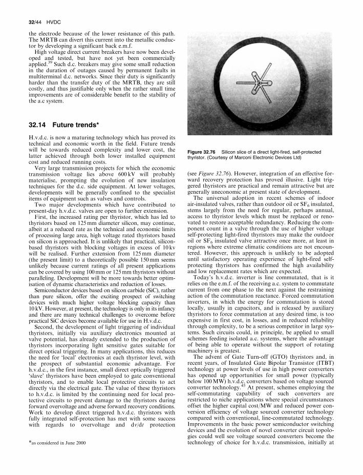
//integras/b&h/Eer/Final_06-09-02/eerc032
32/44 HVDC
the electrode because of the lower resistance of this path. The MRTB can divert this current into the metallic conduc-tor by developing a significant back e.m.f.
High voltage direct current breakers have now been devel-oped and tested, but have not yet been commercially applied.39 Such d.c. breakers may give some small reduction in the duration of outages caused by permanent faults in multiterminal d.c. networks. Since their duty is significantly harder than the transfer duty of the MRTB, they are still costly, and thus justifiable only when the rather small time improvements are of considerable benefit to the stability of the a.c system.
32.14 Future trends*
H.v.d.c. is now a maturing technology which has proved its technical and economic worth in the field. Future trends will be towards reduced complexity and lower cost, the latter achieved through both lower installed equipment cost and reduced running costs.
Very large transmission projects for which the economic transmission voltage lies above 600 kV will probably materialise, prompting the evolution of new insulation techniques for the d.c. side equipment. At lower voltages, developments will be generally confined to the specialist items of equipment such as valves and controls.
Two major developments which have contributed to present-day h.v.d.c. valves are open to further extension.
First, the increased rating per thyristor, which has led to thyristors based on 125 mm diameter silicon, may continue, albeit at a reduced rate as the technical and economic limits of processing large area, high voltage rated thyristors based on silicon is approached. It is unlikely that practical, silicon-based thyristors with blocking voltages in excess of 10 kv will be realised. Further extension from 125 mm diameter (the present limit) to a theoretically possible 150 mm seems unlikely because current ratings of all present applications can be covered by using 100 mm or 125 mm thyristors without paralleling. Development will be more towards better optim-isation of dynamic characteristics and reduction of losses.
Semiconductor devices based on silicon carbide (SiC), rather than pure silicon, offer the exciting prospect of switching devices with much higher voltage blocking capacity than 10 kV. However, at present, the technology is only in its infancy and there are many technical challenges to overcome before practical SiC devices become available for use in H.v.d.c.
Second, the development of light triggering of individual thyristors, initially via auxiliary electronics mounted at valve potential, has already extended to the production of thyristors incorporating light sensitive gates suitable for direct optical triggering. In many applications, this reduces the need for `local' electronics at each thyristor level, with the prospect of substantial economic advantage. For h.v.d.c., in the first instance, small direct optically triggered `slave' thyristors have been employed to gate conventional thyristors, and to enable local protective circuits to act directly via the electrical gate. The value of these thyristors to h.v.d.c. is limited by the continuing need for local pro-tective circuits to prevent damage to the thyristors during forward overvoltage and adverse forward recovery conditions. Work to develop direct triggered h.v.d.c. thyristors with fully integrated self-protection has met with some success with regards to overvoltage and dv/dt protection
*as considered in June 2000
Figure 32.76 Silicon slice of a direct light-fired, self-protected thyristor. (Courtesy of Marconi Electronic Devices Ltd)
(see Figure 32.76). However, integration of an effective for-ward recovery protection has proved illusive. Light trig-gered thyristors are practical and remain attractive but are generally uneconomic at present state of development.
The universal adoption in recent schemes of indoor air-insulated valves, rather than outdoor oil or SF6 insulated, stems largely from the need for regular, perhaps annual, access to thyristor levels which must be replaced or reno-vated to restore acceptable redundancy. Reducing the com-ponent count in a valve through the use of higher voltage self-protecting light-fired thyristors may make the outdoor oil or SF6 insulated valve attractive once more, at least in regions where extreme climatic conditions are not encoun-tered. However, this approach is unlikely to be adopted until satisfactory operating experience of light-fired self-protecting thyristors has confirmed the high availability and low replacement rates which are expected.
Today's h.v.d.c. inverter is line commutated, that is it relies on the e.m.f. of the receiving a.c. system to commutate current from one phase to the next against the restraining action of the commutation reactance. Forced commutation inverters, in which the energy for commutation is stored locally, usually in capacitors, and is released by auxiliary thyristors to force commutation at any desired time, is too expensive in first cost, in losses, and in reduced reliability through complexity, to be a serious competitor in large sys-tems. Such circuits could, in principle, be applied to small schemes feeding isolated a.c. systems, where the advantage of being able to operate without the support of rotating machinery is greatest.
The advent of Gate Turn-off (GTO) thyristors and, in recent years, of Insulated Gate Bipolar Transistor (ITBT) technology at power levels of use in high power converters has opened up opportunities for small power (typically below 100 MW) h.v.d.c. converters based on voltage sourced converter technology.45 At present, schemes employing the self-commutating capability of such converters are restricted to niche applications where special circumstances offset the higher capital cost/MW and reduced power con-version efficiency of voltage sourced converter technology compared with conventional, line-commutated technology. Improvements in the basic power semiconductor switching devices and the evolution of novel converter circuit topolo-gies could well see voltage sourced converters become the technology of choice for h.v.d.c. transmission, initially at

//integras/b&h/Eer/Final_06-09-02/eerc032
References 32/45
low power and later, as technology matures, at increasing levels of power.
The performance of an h.v.d.c. scheme is critically depen-dent on the central control system, particularly if the a.c. sys-tem at the receiving end is weak. The cost of the controls is a small fraction of the overall cost of a scheme, hence improve-ment of control performance and operational reliability will continue even where this incurs somewhat higher costs.
Some parts of the controls will be implemented on pro-grammable digital systems with internal self-checking and, in critical areas, with duplicated circuits and automatic change-over in the event of faults. Because of their relative simplicity and low component count, analogue circuits are likely to be retained in those areas to which they are best suited.
References
1 KIMBARK, E. W., Direct Current Transmission, Vol. 1. Wiley Interscience, New York (1971)
2 THORP and MACGREGOR, Design of the Sea Electrode System, Sardinia±Italian Mainland 200 kV Scheme (IEE Conference Publication No. 22), London (1966)
3 BURGESS, R. P. and KOTHARI, R., Design Features of the Back-to-Back HVDC Convertor Connecting the Western and Eastern Canadian Systems, IEEE July (1989)
4 GAVRILOVIC, A., HVDC Scheme Aspects Influencing Design of Converter Terminals, International Symposium HVDC, Rio de Janeiro (March 1983)
5 IEC, Insulation Co-ordination Application Guide for Insulation Co-ordination and Arrester Protection of HVDC Converter Stations (IEC Publication Nos 71-1 and 71-2), London (1976) (CIGRE WG 33-05, Electra, 96 (1984))
6 GIBSON, H., BALLAD, J. P. and CHESTER, J. K., Characterisation, Evaluation and Modelling of Thyristors for HVDC (IEE Conference Publication No. 255), IEE London (1985)
7 WOODHOUSE, M. L., BALLAD, J. P., HADDOCK, J. L. and ROWE, B. A., `The control and protection of thyristors in the English terminal cross channel valves, particularly during forward recovery', IEE Conference Publication No. 205, Thyristor and Variable Static Equipment for A.C. and D.C. Transmission, IEE, London (1981)
8 CHESTER, J. K., `A new technique for deriving self-consistent electrical and thermal models of thyristors during surge loops', IEE Conference Proceedings, Power Electronics, Power Semi-Conductors and their Applications, IEE, London (1977)
9 EKSTROM, A. and JUHLIN, L. E., Testing of Thyristor Valves, (CIGRE Publication No. 14-03), CIGRE, Paris (1972)
10 BANKS, R., ROWE, B. A. and NOBLE, R. G., Testing Thyristor Valves for HVDC Transmission (CIGRE Publication No. 14-07), CIGRE, Paris (1978)
11 DEMAREST, O. M. and STOILS, C. M., Solid State Valve Test Procedures and Field Correlation (CIGRE Publication No. 14-12), CIGRE, Paris (1978)
12 LIPS, P., THIELE, G., HUYNH, H. and VOHL, P. E., `Design and testing of thyristor valves for the HVDC back-to-back TIE Chateauguay', International Conference on DC Power Transmission, Montreal, Canada (June 1984)
13 INTERNATIONAL ELECTROTECHNICAL COM-MISSION, Publication 700, IEC, Geneva (1981)
14 KRISHNAYYA, P. C. S., Important Characteristics of Thyristors, of Valves for HVDC Transmission and Static Var Compensators, (CIGRE Publication No. 14±10), CIGRE, Paris (1984)
15 CIGRE, Guide for Planning DC Links Terminating at AC Locations having Low Short Circuit Capacities. Part I: AC/DC System Interaction Phenomena, CIGRE Technical Brochure 68, Paris (1992)
16 British Patent 1 300 226. (Current-error characteristic) 17 AINSWORTH, J. D., `The phase-locked oscillatorÐa
new control system for controlled state converters', IEEE Trans., PAS-87(3), 859±865 (March 1968)
18 AINSWORTH, J. D., `Harmonic instability between controlled static converters and a.c. networks', Proc. IEE, 114(7), 949±958 (July 1967)
19 AINSWORTH, J. D., `Developments in the phase-locked oscillator control system for HVDC and other large converters', IEE Conference on a.c. and d.c. Power Transmission. IEE Conference Publication No. 255 (September 1985)
20 British Patents 1 170 249 and 1 258 974 (Master control and telecommunication)
21 AINSWORTH, J. D., `Telecommunication for HVDC', IEE Conference on Thyristor and Variable Static Equipment for a.c. and d.c. Transmission, IEE Conference Publication No. 205, (November 1981)
22 MARTIN, C. J. B. and UHLMANN, E., AC Network Stabilisation by DC Links (CIGRE Paper 32-01), CIGRE, Paris (1970)
23 HAYWOOD, R. W. and RALLS, K. J., Use of HVDC for Improving AC System Stability and Speed Control, Manitoba Power Conference EHV-DC, Winnipeg, Manitoba (June 1971)
24 AINSWORTH, J. D. and MARTIN, G. J. B., `The influence of h.v.d.c. links on a.c. power systems', GEC Journal of Science and Technology, 44(1), (1977)
25 CIGRE, Guide for Planning DC Links Terminating at AC Locations having Low Short Circuit Capacities. Part I: AC/DC System Interaction Phenomena, CIGRE Technical Brochure 68, Paris (1992)
26 GAVRILOVIC, A., KRISHNAYYA, P. C. S., PEIXOTO, C. O. A., AINSWORTH, J. D., BOWLES, J. P., HAMMAD, A., LISS, G. and THIO, C. V., Aspects of a.c./d.c. System Interactions: Peak Available Power, Second Harmonic Resonance, Low Inertia Systems, Controllability of h.v.d.c., MONTECH-IEEE Conference (September±October 1986)
27 GAVRILOVIC, A., KRISHNAYYA, P. C. S., AINSWORTH, J. D., BOWLES, J. P., BREUER, G. D., HAMMAD, A., LISS, G., PEIXOTO, C. O. A., POVH, D. and THIO, C. D., ̀Interaction between a.c and d.c. systems', CIGRE Symposium: AC/DC Transmission Interactions and Comparisons', Boston (September 1987)
28 GAVRILOVIC, A., HVDC Scheme Aspects Influencing the Design of Converter Terminals, International Symposium on HVDC Technology, Rio de Janeiro (March 1983)
29 THANAWALA, H. L., Maximum Available Power Features of a.c. and d.c. Transmission Systems, Power Technology International (1990)
30 LISS, G. and SMEDSFELT, S., HVDC Links for Connection to Isolated a.c. Networks, United Nations Seminar on High Voltage Direct Current (HVDC) Techniques (May 1985)
31 AINSWORTH, J. D. and GAVRILOVIC, A., Interaction Between HVDC and a.c. Systems when the d.c. Link is Large Compared to the a.c. System, United

//integras/b&h/Eer/Final_06-09-02/eerc032
32/46 HVDC
Nations Seminar on High Voltage Direct Current (HVDC) Techniques, Stockholm (May 1985)
32 AINSWORTH, J. D., GAVRILOVIC, A. and THANAWALA, H. L., Static and Synchronous Compensators for h.v.d.c. Transmission Converters Connected to Weak a.c. Systems (CIGRE Paper No. 31-01), CIGRE, Paris (August 1980)
33 HAMMAD, A. and KAENFERLE, J., A New Approach for the Analysis and Solutions of a.c. Voltage StabilityÐProblems at h.v.d.c. Terminals, HVDC Symposium, Montreal, Canada (June 1984)
34 AINSWORTH, J. D., Development in the Phase-locked Oscillator Control Systems for HVDC and Other Large Converters (IEE Conference Publication No. 255), London (1985)
35 PIKE, P. J. and LARSEN, E. V., HVDC System Control for Damping of Subsynchronous Oscillations (IEEE PZS-101) (July 1982)
36 CARCANO, C., INESI, A., MAZZOLDI, F. and RICCI, F., Rebuilding of the h.v.d.c. Sardinia± Corsica±Italy Mainland Link (SACOI): Installation of Two New Conversion Stations and a Tapping Station in Corsica for Multi-terminal Operation. (IEE Conference Publication No. 255), IEE, London (1985)
37 AINSWORTH, J. D., Multi-terminal h.v.d.c. Systems (CIGRE Meeting SC.14), Winnipeg, Canada (June 1977)
38 LONG, W. F., REEVE, J. M'NICHOL, J. R., HARRISON, R. E. and BOWLES, J. P., Considerations for Implementing Multi-terminal d.c. Systems, W. F. Long, IEEE PES Winter Meeting (1985)
39 VITHAYATHIL, J. J., HVDC Breaker and its Application, International Symposium in HVDC Technology, Rio de Janeiro, Brazil (March 1983)
40 MELTA, H. and TEMPLE, V. A., Advanced Light-triggered Thyristor, A.c. and d.c. Power Transmission Conference (IEE Conference Publication No. 255), London (1985)
41 TAYLOR. P. D. and FRITH, P. J., Recent Advances in High Voltage Thyristor Design, A.c. and d.c. Power Transmission Conference (IEE Conference Publication No. 255), London (1985)
42 NISHIZAURA, J., New Thyristor Applicable to d.c. Power Transmission, A.c. and d.c. Power Transmission Conference (IEE Conference Publication No. 255), London (1985)
43 THANAWALA, H. L., WHITEHOUSE, R. S., GOO OURCK KWON and SUK JIN LEE, Equipment and control features of Haenam±Cheju Link in South Korea, (CIGRE Paper 14-303), CIGRE, Paris (1994)
44 MAZZOLDI, F., TAISNE, J.-P., MARTIN, C. J. B. and ROWE, B. A., Adaptation of the Control Equipment to permit 3-terminal operation of the HVDC link between Sardinia, Corsica and Mainland Italy, IEE Summer Power Meeting (1988)
45 APSLUND, G., ERIKSON, K., JIANG, H., LINDBERG, J., PALSSON, R. and SVENSSON, K., DC Transmission based on Voltage Source Convertors, (CIGRE Paper 14-302), CIGRE, Paris (1998)
Bibliography
An Annotated Bibliography of High Voltage Direct Current Transmission, 1969±1983, Bonneville Power Administration An Annotated Bibliography of High Voltage Direct Current Transmission, 1984±1989, Western Area Power Administration, Bonneville Power Administration An Annotated Bibliography of High Voltage Direct Current Transmission, 1989±1991, Western Area Power Administration, Bonneville Power Administration An Annotated Bibliography of High Voltage Direct Current Transmission and Flexible AC Transmission (FACTS) Devices, 1991±1993, Bonneville Power Administration, Western Area Power Administration An Annotated Bibliography of HVDC Transmission and FACTS Devices, 1994±1995, US Department of Energy, Western Area Power Administration. An Annotated Bibliography of HVDC Transmission and FACTS Devices, 1996±1997, EPRI and Bonneville Power Administration
IEE Publications
IEEE 857 The Testing of Thyristor Valves for HVDC:(1996)International Conference on DC Power Transmission,Montreal, Canada (1984)Overvoltages and compensation on integrated a.c./d.c. sys-tems, (IEEE Conference Proceedings), Winnipeg, Canada (June 1980)
Conferences other than CIGRE, IEE, IEEE
International Symposium on HVDC Technology±Sharing theBrazilian Experience, Rio de Janeiro (1983)Manitoba Power Conference EHV-DC, Winnipeg, Canada(1971)US DEPARTMENT OF ENERGY, Incorporating HVDCPower Transmission into Power System Planning, Phoenix,Arizona (1980)
Books by individual authors
ADAMSON, C., and HINGORANI, N. G., High VoltageDirect Current Power Transmission, Garraway, London(1960)ARRILLAGA, J., High Voltage Direct CurrentTransmission (IEE Power Engineering Series 6) PeterPeregrinus, London (1983)CORY, B. J. (Ed.), High Voltage Direct Current Convertorsof Systems, Macdonalds, London (1965)KIMBARK, E. W., Direct Current Transmission, Vol. 1,Wiley Interscience, New York (1971)UHLMANN, E., Power Transmission by Direct Current,Springer-Verlag, Berlin (1975)