3.2. intrinsic semiconductors
TRANSCRIPT

3.2. Intrinsic semiconductors:
Unbroken covalent bonds make a low conductivity crystal, and at 0ok the
crystal behaves as an insulator, since no free electrons and holes are
available. At room temperature, some of the covalent bonds will be
broken because of the thermal energy supplied to the crystal and
conductive increases since pairs of (e-h) are thermally generated. A
forbidden energy EG or energy gap is required to break such a covalent
bond where EG=0.72 eV for Ge and EG=1.1 eV for Si at room
temperature (300ok). When a bond is broken so that a hole is exist, it is
easy for a valence -e in a neighboring atom to leave its covalent bond in
order to fill this hole, which in turn leaves a hole in its original position.
Hence, holes move in opposite direction to that of -e. Hence, holes can
participate in the conduction of electricity. Holes behave like a (+ve)
charge so that hole current is in the same direction as hole movement.
If n≡ no. of electrons in C.B (thermally generated)
p≡ no. of holes in V.B (thermally generated)
So n=p=ni=pi................. in intrinsic semiconductors.
Where ni=pi ≡ intrinsic concentration of electrons (holes).
Conductivity of intrinsic semiconductor is due to both -e and holes:
𝜎 = 𝑞𝑛𝜇𝑛 + 𝑞𝑝𝜇𝑝
𝜎𝑖 = 𝑞𝑛𝑖𝜇𝑛 + 𝑞𝑝𝑖𝜇𝑝 𝑏𝑢𝑡 𝑛𝑖 = 𝑝𝑖
∴ 𝜎𝑖 = 𝑞𝑛𝑖 𝜇𝑛 + 𝜇𝑝 𝑖𝑛𝑡𝑟𝑖𝑛𝑠𝑖𝑐 𝑐𝑜𝑛𝑑𝑢𝑐𝑡𝑖𝑣𝑖𝑡𝑦
Where µn ≡ mobility of -e in C.B.
µp ≡ mobility of holes in V.B.
And
𝑛𝑖𝑝𝑖 = 𝑛𝑖2

3.3. Extrinsic semiconductors:
If a small percentage of trivalent or pentavalent atoms are added to
intrinsic Si or Ge, impure or extrinsic semiconductor is formed.
3.3.1. N-type semiconductor:
Donor impurities (or pentavalent atom) such as Phosphorous p (z=15);
Arsenic As (z=33); Antimony Sb (z=51); and Bismuth B (z=83).
EV ≡ upper energy level of V.B. C.B.
EC ≡ lower energy level of C.B.
ED ≡ donor energy. + + + + + + + + + +
EC - ED =0.01 eV for Ge EG donor energy (+ve)
=0.05 eV for Si
This energy is required to detached
the fifth electron from the impurity atom.
The no. of -e in C.B. (n) increase rapidly due to V.B.
the impurity, the holes decrease comparing with the intrinsic hole
concentration (pi) because the rate of recombination between -e and hole
will increase. Therefore, majority carriers’ electrons (nn) and minority
carrier holes (pn).
nn= Nd + ni and Nd >> ni
Nd ≡ donor doping concentration.
n
Ionization n region
Nd intrinsic region
Extrinsic region
p
0 ~50ok ~500
ok
Tok
EC
ED
EV

3.3.2. P-type semiconductor:
Acceptor impurities (trivalent atoms) such as Boron B (z=5); Indium In
(z=49); Gallium Ga (z=31); Alliminum Al (z=13).
EA ≡ acceptor energy level.
EA - EV = 0.01 eV for Ge C.B. Ec
= 0.05 eV for Si
Since a very small amount of energy is
required for an (-e) to leave the V.B. and Acceptor energy level (-ve)
fill the acceptor energy level. So generated - - - - - - - - - - - - - - EA
holes in V.B. and is equal to the no. of the EV
impurity concentration (Na). Therefore, majority V.B.
carriers holes (pp) and minority carries electrons (np).
pp = Na + pi and Na >> pi
Na ≡ acceptor doping concentration.
p
p
Na
n
50 500
Tok

3.7. Mass action law:
At thermal equilibrium (at room temperature), the product of the free
electron and hole concentration is constant and is independent of the
amount of donor and acceptor impurity.
nipi = pnnn = ppnp = ni2
𝑝𝑛 =𝑛𝑖
2
𝑛𝑛≈
𝑛𝑖2
𝑁𝐷
𝑛𝑝 =𝑛𝑖
2
𝑝𝑝≈
𝑛𝑖2
𝑁𝐴
The current density (J)
𝐽 = 𝜎𝐸 = 𝑞 𝑛𝜇𝑛 + 𝑝𝜇𝑝 𝐸
3.4. Conductivity of extrinsic semiconductor:
Assume that ni= intrinsic electron concentration.
pi = intrinsic hole concentration.
nn= electron concentration in n-type.
pn= hole concentration in n-type.
ND= donor electrons.
Pp= hole concentration in p-type.
np= electron concentration in p-type.
NA= acceptor holes.
In n-type:
𝑛 + 𝑁𝐴− = 𝑝 + 𝑁𝐷
+
𝑛𝑛 = 𝑛𝑖 + 𝑁𝐷
𝜎 = 𝑞 𝑛𝑛𝜇𝑛 + 𝑝𝑛𝜇𝑝 𝑒𝑥𝑎𝑐𝑡 𝑣𝑎𝑙𝑢𝑒 𝑜𝑓 𝑐𝑜𝑛𝑑𝑢𝑐𝑡𝑖𝑣𝑖𝑡𝑦
At normal temperature (extrinsic region), ND >> ni and nn >> pn so that
nn ~ ND.
𝜎 ≅ 𝑞𝑁𝐷𝜇𝑛 𝑎𝑝𝑝𝑟𝑜𝑥𝑖𝑚𝑎𝑡𝑒 𝑐𝑜𝑛𝑑𝑢𝑐𝑡𝑖𝑣𝑖𝑡𝑦
In p-type:
𝑝𝑝 = 𝑝𝑖 + 𝑁𝐴
𝜎 = 𝑞 𝑝𝑝𝜇𝑝 + 𝑛𝑝𝜇𝑛
At normal temperature, NA >> pi and pp >> np so that pp ~ NA.
𝜎 ≅ 𝑞𝑁𝐴𝜇𝑃
3.5. Charge neutrality relationship:
The relationships established to this point are devoid of an explicit
dependence on the dopant concentrations introduction into a
semiconductor. It is the charge neutrality relationship that provides the

general tie between the carrier and dopant concentrations. To establish
the charge neutrality relationship, let us consider a uniformly doped
semiconductor, a semiconductor where the number of dopant atoms/cm3
is the same everywhere. Systematically examining little sections of the
semiconductor far from any surfaces, and assuming equilibrium
conditions prevail; one must invariably find that each and every section is
charge-neutral, i.e, contains no net charge. If this were not the case,
electric fields would exist inside the semiconductor. The electric fields in
turn would give rise to carrier motion and associated currents- a situation
totally inconsistent with the assumed equilibrium conditions. There are,
however, charged entities inside all semiconductors. Electrons, holes,
ionized donors (donor atoms that have become positively charged by
donating an electron to the conduction band) and negatively charged
ionized acceptors can all exist simultaneously inside any given
semiconductor. For the uniformly doped material to be everywhere
charge neutral clearly requires.
𝑐𝑎𝑟𝑔𝑒
𝑐𝑚3 = 𝑞𝑝 − 𝑞𝑛 + 𝑞𝑁𝐷+ − 𝑞𝑁𝐴
− = 0
𝑜𝑟 𝑝 − 𝑛 + 𝑁𝐷+ − 𝑁𝐴
− = 0
Where, by definition,
𝑁𝐷+ =number of ionized (positively charged) donors/cm
3.
𝑁𝐴− =number of ionized (negatively charged) acceptors/cm
3.
As previously discussed, there is sufficient thermal energy available in a
semiconductor at room temperature to ionize almost all of the shallow-
level donor and acceptor sites. Defining:
ND =total number of donors/cm3.
NA =total number of acceptors/cm3.
And setting
𝑁𝐷+ = 𝑁𝐷
𝑁𝐴− = 𝑁𝐴
One then obtains
𝒑 − 𝒏 + 𝑵𝑫 − 𝑵𝑨
= 𝟎 𝒂𝒔𝒔𝒖𝒎𝒆𝒔 𝒕𝒐𝒕𝒂𝒍 𝒊𝒐𝒏𝒊𝒛𝒂𝒕𝒊𝒐𝒏 𝒐𝒇 𝒅𝒐𝒑𝒂𝒏𝒕 𝒂𝒕𝒐𝒎………… . (𝟏)
Equation above is the standard form of the charge neutrality relationship.
3.6. Carrier concentration calculations:
We are finally in a position to calculate the carrier concentrations in a
uniformly doped semiconductor under equilibrium conditions. In the

computations to be presented we specifically make the assumptions of
nondegeneracy (allowing us to use the np product relationship) and total
ionization of the dopant atoms. Note that ni, which appears in the np
product expression, has been calculated and plotted and must be
considered a known quantity. Likewise, NA and ND, which appear in the
charge neutrality relationship, are typically controlled and determined
experimentally and should also be considered known quantities. The only
other symbols used the two equations are n and p. thus, under the cite
assumptions of nondegeneracy and total ionization of dopant atoms, we
have two equations and two unknowns from which n and p can be
deduced. Starting with the np product expression, one can write:
𝑝 =𝑛𝑖
2
𝑛……………………………………………… . . 2
Eliminating p in eq. (1) using eq. (2) gives:
𝑛𝑖2
𝑛− 𝑛 + 𝑁𝐷 − 𝑁𝐴 = 0 ………………………………… . . 3
Or
𝑛2 − 𝑛 𝑁𝐷 − 𝑁𝐴 − 𝑛𝐼2 = 0
Solving the quadratic equation for n then yields:
𝑛 =𝑁𝐷 − 𝑁𝐴
2+
𝑁𝐷 − 𝑁𝐴
2
2
+ 𝑛𝑖2
12
………………………… . 4𝑎
And
𝑝 =𝑛𝑖
2
𝑛=
𝑁𝐴 − 𝑁𝐷
2+
𝑁𝐴 − 𝑁𝐷
2
2
+ 𝑛𝑖2
12
……………………… . . 4𝑏
Only the plus roots have been retained in Esq. (4) because physically the
carrier concentrations must be greater than or equal to zero.
Equations (4) are general case solutions. In the vast majority of practical
computations it is possible to simplify these equations prior to
substituting in numerical values for ND, NA, and ni. Special cases of
specific interest are considered next.
(1) Intrinsic semiconductor (NA=0, ND=0). With NA=0 and ND=0, Esq. (4)
simplify to n=ni and p=ni. n=p=ni is of course the expected result for the
equilibrium carrier concentrations in an intrinsic semiconductor.
(2) Doped semiconductor where either ND - NA ≈ ND>> ni or NA - ND ≈
NA>>ni . This is the special case of greatest practical interest. The
unintentional doping levels in Si are such that the controlled addition of
dopants routinely yields ND>> NA or NA>> ND. Moreover, the intrinsic
carrier concentration in Si at room temperature is about 1010
/cm3, while
the dominant doping concentration (NA or ND) is seldom less than
1014
/cm3. Thus the special case considered here is the usual case
encountered in practice. If ND-NA ≈ ni, the square root in eq. (4a) reduces
to ND/2 and:
𝑛 ≈ 𝑁𝐷 ……………………………………………………… . 5𝑎
𝑝 ≈ 𝑛𝑖2 𝑁𝐷 ……………………………………………………… 5𝑏
ND>>NA, ND>> ni (nondegenerate, total ionization)
Similarly
𝑝 ≈ 𝑁𝐴 ……………………………………………………… 6. 𝑎
𝑛 ≈ 𝑛𝑖2 𝑁𝐴 ………………………………………………………… 6. 𝑏
NA>>ND , NA>> ni (nondegenerate, total ionization)
As a numerical example, suppose a Si sample maintained at room
temperature is uniformly doped with ND=1015
/cm3 donors. Using Eqs.(5),
one rapidly concludes n≈1015
/cm3 and p≈10
5/cm
3.
(3) Doped semiconductor where ni >> |ND-NA|. Systematically increasing
the ambient temperature causes a monotonic rise in the intrinsic carrier
concentration. At sufficiently elevated temperatures, ni will eventually
equal and then exceed the net doping concentration. If ni>>|ND-NA|, the
square roots in Eqs. (4) reduce to ni and n≈p≈ni . in other words, all
semiconductors become intrinsic at sufficiently high temperatures where
ni>>|ND-NA|.
(4) Compensated semiconductor. As is evident from Eqs. (4), donors and
acceptors tend to negate each other. Indeed, it is possible to produce
intrinsic like material by making ND-NA=0. In some materials, such as
GaAs, NA may be comparable to ND in the as grown crystal. When NA and
ND are comparable and nonzero, the material is said to be compensated. If
the semiconductor is compensated, both NA and ND must be retained in all
carrier concentration expressions.
In summary Eqs. (4) can always be used to compute the carrier
concentrations if the semiconductor is nondegerated and the dopant are
totally ionized. In the vast majority of practical situations, however, it is
possible to simplify these equations prior to performing numerical
computations. Equations (4) must be used to compute the carrier
concentrations only in those rare instances when |ND-NA| ~ ni the
simplified relationships of greatest practical utility are Eqs. (5) and (6).


4. Fermi-Dirac probability function (f(E)):
The Fermi-Dirac probability function f(E), gives the probability that a
state of energy (E) is occupied by electron.
𝑓 𝐸 =1
1 + 𝑒 𝐸−𝐸𝐹𝑘𝑇
Where k= Boltzmann constant = 1.38*10-23
J/oK =8.62*10
-5 eV/
oK.
T= temperature in oK.
EF= is the Fermi-level, which represent the energy state with 50%
probability of being filled with (-e) if no forbidden band exist and is
independent of temperature. i.e. when E=EF:
𝑓 𝐸 =1
1 + 𝑒 𝐸𝐹−𝐸𝐹
𝑘𝑇
=1
1 + 𝑒0=
1
1 + 1=
1
2= 0.5 = 50%
At T=0ok:
0 if E>EF (C.B) no (-e) in C.B. so that f (E) =0.
f(E)=
1 if E<EF (V.B) all energies in V.B. are occupied by (-e).
In any metal: Fermi energy at 0ok is:
𝐸𝑓𝑜 =2
8𝑚
3𝑛
𝜋
23
………… . . 𝑗𝑜𝑢𝑙𝑒
n= electron density.
Or Efo = 3.64*10-19
n2/3
(eV)
At any temperature (T):
𝐸𝑓 = 𝐸𝑓𝑜 1 −𝜋2
12 𝑘𝑇
𝐸𝑓𝑜
2
i.e Ef as T , 𝜎 in metals since Ef .
f (E)
1 T=0oK
T= 300oK
T=2500oK
0.5

0 E
E=Ef
E< EF (V.B) | E> Ef (C.B)
4.1. Derivation of the Fermi-Dirac distribution function:
To derive the Fermi-Dirac distribution function, we start from a series of
possible energies, labeled Ei. At each energy, we can have gi possible
states and the number of states that are occupied equals gifi, where fi is the
probability of occupying a state at energy Ei. We also assume that number
of possible states is very large, so that the discrete nature of the state can
be ignored. The number of possible ways called configurations to fit gi fi
electrons in gi states, given the restriction that only one electron can
occupy each state, equals:
𝑊𝑖 =𝑔𝑖
𝑔𝑖 − 𝑔𝑖𝑓𝑖 ! 𝑔𝑖𝑓𝑖!…………………………………………… . 1
This equation is obtained by numbering the individual states and
exchanging the states rather than the electrons. This yields a total number
of gi! possible configurations. However since the empty states are all
identical, we need to divide by the number of permutations between the
empty states, as all permutations cannot be distinguished from each other
and can therefore only be counted once. In addition, all the filled states
are indistinguishable from each other, so we need to divide also by all
permutations between the filled states, namely gifi! The number of
possible ways to fit the electrons in the number of available states is
called the multiplicity function. The multiplicity function for the whole
system is the product of the multiplicity functions for each energy Ei:
𝑊 = 𝑊𝑖
𝑖
= 𝑔𝑖 !
𝑔𝑖 − 𝑔𝑖𝑓𝑖 ! 𝑔𝑖𝑓𝑖 !𝑖
…………………………… . . 2
Using Stirling’s approximation, one can eliminate the factorial signs,
yielding:

𝑙𝑛𝑊 = 𝑙𝑛𝑊𝑖
𝑖
= 𝑔𝑖 𝑙𝑛𝑔𝑖 − 𝑔𝑖 1 − 𝑓𝑖 ln 𝑔𝑖 − 𝑔𝑖𝑓𝑖 − 𝑔𝑖𝑓𝑖𝑙𝑛𝑔𝑖𝑓𝑖
𝑖
3
The total number of electrons in the system equals N and the total energy
of those N electrons equal U. These system parameters are related to the
number of states at each energy, gi, and the probability of occupancy of
each state, fi, by:
𝑁 = 𝑔𝑖𝑓𝑖
𝑖
……………………………………………………………… 4
And
𝑈 = 𝐸𝑖𝑔𝑖𝑓𝑖𝑖
……………………………………………………………… (5)
According to the basic assumption of statistical thermodynamics, all
possible configurations are equally probable. The multiplicity function
provides the number of configurations for a specific sat of occupancy
probabilities, fi. The multiplicity function sharply peaks at the thermal
equilibrium distribution since this is the most likely distribution of the
system and must therefore be associated with the largest number of
equally probable configurations. The occupancy probability in thermal
equilibrium is therefore obtained by finding the maximum of the
multiplicity function, W, while keeping the total energy and the number
of electrons constant. For convenience, we maximize the logarithm of the
multiplicity function instead of the multiplicity function itself. According
to the Lagrange method of undetermined multipliers, we must maximize
the following function:
ln 𝑊 − 𝑎 𝑔𝑗𝑓𝑗𝑗
− 𝑏 𝐸𝑗𝑔𝑗𝑓𝑗𝑗
……………………………………… . 6
Where a and b need to be determine. The maximum of the multiplicity
function, W, is obtained from:
𝜕
𝜕 𝑔𝑖𝑓𝑖 𝑙𝑛𝑊 − 𝑎 𝑔𝑖𝑓𝑖
𝑗
− 𝑏 𝐸𝑗𝑔𝑗𝑓𝑗𝑗
= 0 ……………………… . 7
which can be solved, yielding:
𝑙𝑛𝑔𝑖 − 𝑔𝑖𝑓𝑖
𝑔𝑖𝑓𝑖− 𝑎 − 𝑏𝐸𝑖 = 0 ………………………………………… . (8)
Or
𝑓𝑖 = 𝑓𝐹𝐷 𝐸𝑖 =1
1 + exp 𝑎 + 𝑏𝐸𝑖 ……………………………………… . 9
Which can be written in the following form
𝑓𝐹𝐷 𝐸𝑖 =1
1 + exp 𝐸𝑖 − 𝐸𝐹
𝛽 ………………………………………… . . 10
With b=1/b and EF= -a/b. The symbol EF was chosen since this constant
has units of energy and will be the constant associated with this
probability distribution. Taking the derivative of the total energy, one
obtains:
𝑑𝑈 = 𝐸𝑖𝑑 𝑔𝑖𝑓𝑖
𝑖
+ 𝑔𝑖𝑓𝑖𝑑𝐸𝑖
𝑖
……………………………………… . (11)
Using the Lagrange equation, this can be rewritten as:
𝑑𝑈 = 𝛽𝑑 𝑙𝑛𝑊 + 𝑔𝑖𝑓𝑖𝑑𝐸𝑖
𝑖
+ 𝐸𝐹𝑑𝑁 ………………………………… (12)
Any variation of the energies, Ei, can only be caused by a change in
volume, so that the middle term can linked to a volume variation dV.
𝑑𝑈 = 𝛽𝑑 𝑙𝑛𝑊 + 𝑔𝑖𝑓𝑖𝑑𝐸𝑖
𝑑𝑉𝑖
𝑑𝑉
+ 𝐸𝐹𝑑𝑁 …………………………… . (13)
Comparing this to the thermodynamic identity:
𝑑𝑈 = 𝑇𝑑𝑆 − 𝑝𝑑𝑉
+ 𝜇𝑑𝑁………………………………………………… 14
One finds that b=kT and S=k ln W, where k is a constant that must be
determined. The energy, EF, equals the energy associated with the
particles, namely the electro-chemical potential, m. the comparison also
identifies the entropy, S, as being proportional to the logarithm of the
multiplicity function, W. the proportionality constant, k, is known as
Boltzmann’s.
The Fermi- Dirac distribution function then becomes:
𝑓𝐹𝐷 𝐸
=1
1 + exp 𝐸 − 𝐸𝐹
𝑘𝑇 ……………………………………………… . 15
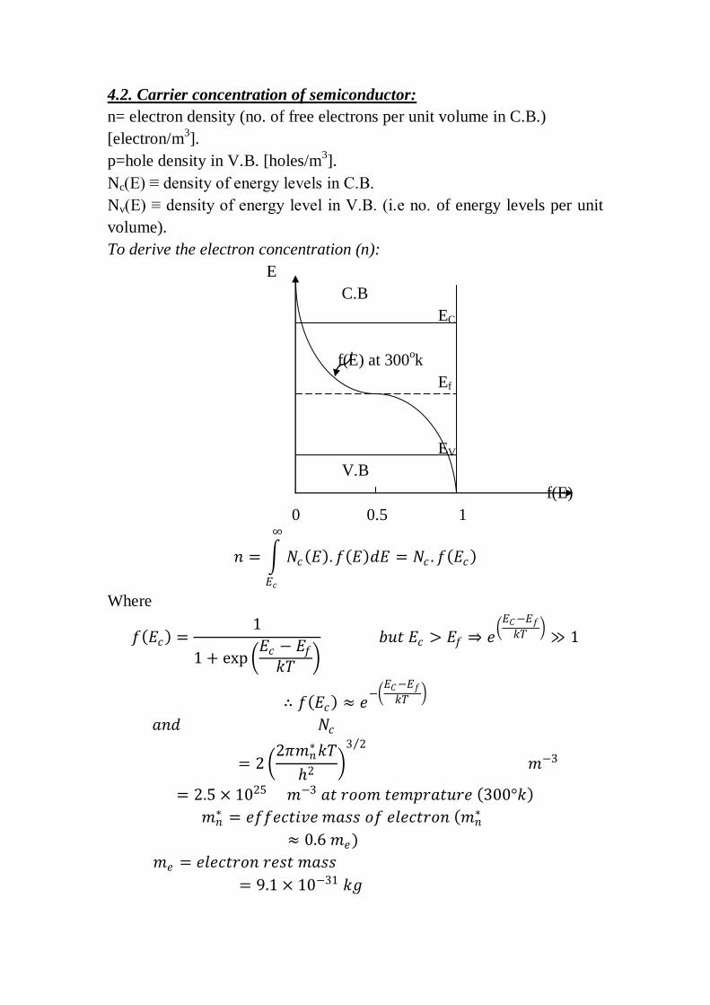
4.2. Carrier concentration of semiconductor:
n= electron density (no. of free electrons per unit volume in C.B.)
[electron/m3].
p=hole density in V.B. [holes/m3].
Nc(E) ≡ density of energy levels in C.B.
Nv(E) ≡ density of energy level in V.B. (i.e no. of energy levels per unit
volume).
To derive the electron concentration (n):
E
C.B
EC
f(E) at 300ok
Ef
EV
V.B
f(E)
0 0.5 1
𝑛 = 𝑁𝑐 𝐸 . 𝑓 𝐸 𝑑𝐸 = 𝑁𝑐 . 𝑓 𝐸𝑐
∞
𝐸𝑐
Where
𝑓 𝐸𝑐 =1
1 + exp 𝐸𝑐 − 𝐸𝑓
𝑘𝑇
𝑏𝑢𝑡 𝐸𝑐 > 𝐸𝑓 ⇒ 𝑒 𝐸𝐶−𝐸𝑓
𝑘𝑇 ≫ 1
∴ 𝑓 𝐸𝑐 ≈ 𝑒−
𝐸𝐶−𝐸𝑓
𝑘𝑇
𝑎𝑛𝑑 𝑁𝑐
= 2 2𝜋𝑚𝑛
∗𝑘𝑇
2
3 2
𝑚−3
= 2.5 × 1025 𝑚−3 𝑎𝑡 𝑟𝑜𝑜𝑚 𝑡𝑒𝑚𝑝𝑟𝑎𝑡𝑢𝑟𝑒 300°𝑘
𝑚𝑛∗ = 𝑒𝑓𝑓𝑒𝑐𝑡𝑖𝑣𝑒 𝑚𝑎𝑠𝑠 𝑜𝑓 𝑒𝑙𝑒𝑐𝑡𝑟𝑜𝑛 𝑚𝑛
∗
≈ 0.6 𝑚𝑒
𝑚𝑒 = 𝑒𝑙𝑒𝑐𝑡𝑟𝑜𝑛 𝑟𝑒𝑠𝑡 𝑚𝑎𝑠𝑠
= 9.1 × 10⁻³¹ 𝑘𝑔

𝑛 = 𝑁𝑐𝑒−
𝐸𝑐−𝐸𝑓
𝑘𝑇 applied for both intrinsic and extrinsic.
To drive the hole concentration (p):
𝑝 = 𝑁𝑉 𝐸
𝐸𝑣
−∞
1 − 𝑓 𝐸 𝑑𝐸 = 𝑁𝑉 1 − 𝑓 𝐸𝑉
Where
𝑓 𝐸𝑉 : Probability of energy level being filled but electron in V.B.
1 − 𝑓 𝐸𝑉 : Probability of energy level being empty of electron in V.B.
or probability of energy level being filled by holes (V.B).
1 − 𝑓 𝐸𝑉 = 1 −1
1 + 𝑒 𝐸𝑉−𝐸𝑓
𝑘𝑇
=1
1 + 𝑒 𝐸𝑓−𝐸𝑉
𝑘𝑇
𝑠𝑖𝑛𝑐𝑒 𝐸𝑓 > 𝐸𝑉 ∴ 𝑒 𝐸𝑓−𝐸𝑉
𝑘𝑇 ≫ 1 𝑜𝑟 1 − 𝑓 𝐸𝑉 = 𝑒
𝐸𝑉−𝐸𝑓
𝑘𝑇
= 𝑒−
𝐸𝑓−𝐸𝑉
𝑘𝑇
𝑎𝑛𝑑 𝑁𝑉 = 2 2𝜋𝑚𝑃
∗𝑘𝑇
2
3 2
𝑚𝑝∗ = 𝑒𝑓𝑓𝑒𝑐𝑡𝑖𝑣𝑒 𝑚𝑎𝑠𝑠 𝑜𝑓 𝑜𝑙𝑒𝑠, 𝑤𝑒𝑛 𝑚𝑝
∗ = 𝑚𝑛∗ ⇒ 𝑁𝑉 = 𝑁𝐶 .
𝑝 = 𝑁𝑉𝑒−
𝐸𝑓−𝐸𝑉
𝑘𝑇
applied for both intrinsic and extrinsic.
Homework:
1- Show that the product of n and p is independent of Fermi energy.
2- Derive the equation for the position of Fermi level in intrinsic
semiconductor (Ef i ).
3- Show that the intrinsic concentration ni is given by:
𝑛𝑖 = 𝑁𝐶𝑁𝑉 1 2 exp −𝐸𝐺
2𝑘𝑇
Note:
Atomic density (atoms/cm3) =Avogadro’s no.*
𝑑𝑒𝑛𝑠𝑖𝑡𝑦
𝑎𝑡𝑜𝑚𝑖𝑐 𝑤𝑒𝑖𝑔𝑡
Where Av.no. = 6.02* 1023
atom/mole
Density = gm/cm3.
Atomic weight = gm/mole.
n= atomic density * valence electrons electron/cm3.
4.3. Fermi-level position in extrinsic semiconductor:
In n-type:
𝑛 = 𝑁𝐶 𝑒−
𝐸𝐶−𝐸𝑓
𝑘𝑇
𝑏𝑢𝑡 𝑛~ 𝑁𝐷
∴ 𝑁𝐷 = 𝑁𝐶 𝑒−
𝐸𝐶−𝐸𝑓
𝑘𝑇
⇒ 𝑁𝐷
𝑁𝐶= 𝑒
− 𝐸𝐶−𝐸𝑓
𝑘𝑇
By taking (ln) for both sides:
− 𝐸𝐶 − 𝐸𝑓
𝑘𝑇 = 𝑙𝑛
𝑁𝐷
𝑁𝐶 ⟹ 𝐸𝐶 − 𝐸𝑓𝑛 = 𝑘𝑇 𝑙𝑛
𝑁𝐶
𝑁𝐷
Or
𝐸𝑓𝑛 = 𝐸𝐶 − 𝑘𝑇 𝑙𝑛 𝑁𝐶
𝑁𝐷
𝐼𝑓 𝑁𝐶 = 𝑁𝐷 ⟹ 𝑙𝑛 𝑁𝐶
𝑁𝐷 = 0 𝑖. 𝑒 𝐸𝑓 = 𝐸𝐶(𝐸𝑓 𝑐𝑜𝑖𝑛𝑐𝑖𝑑𝑒𝑠 𝑤𝑖𝑡ℎ 𝐸𝐶)
In p-type:
𝑝 = 𝑁𝑉 𝑒−
𝐸𝑓−𝐸𝑉𝑘𝑇
𝑏𝑢𝑡 𝑝~ 𝑁𝐴
∴ 𝑁𝐴 = 𝑁𝑉 𝑒−
𝐸𝑓−𝐸𝑉𝑘𝑇
⇒
𝑁𝐴
𝑁𝑉= 𝑒
− 𝐸𝑓−𝐸𝑉𝑘𝑇
By taking (ln) for both sides:
𝐸𝑓𝑃 − 𝐸𝑉 = 𝑘𝑇 𝑙𝑛 𝑁𝑉
𝑁𝐴
Or
𝐸𝑓𝑃 = 𝐸𝑉 + 𝑘𝑇 𝑙𝑛 𝑁𝑉
𝑁𝐴
The Fermi level (Ef) in extrinsic semiconductor is slightly depends on
temperature T. But mainly depends on impurity, concentration (NA or
ND).
If ND is added to a crystal at a given temperature, the no. of (e-h) pairs
thermally generated will be reduced. So Ef must move closer to the C.B
to indicate that many of the energy states in that band are filled by donor
electrons and fewer holes exist in V.B.
6. Einstein relationship:
Diffusion constant and mobility are dependent parameters. Einstein
equation: 𝐷𝑝
𝜇𝑝=
𝐷𝑛
𝜇𝑛=
𝑘𝑇
𝑞= 𝑉𝑇 =
𝑇
11600 𝑣𝑜𝑙𝑡
Where VT = volt equivalent of temperature.
Example for Ge Dn=0.0093 m2/s and DP=0.0044 m
2/s.

7. P-N Junction:
Pn junction is used to build: diode, LED, transistors and integrated circuit
(IC).
7.1. Open circuited p-n junction:
If donor impurities ND are introduce into one side and acceptor impurities
NA into other side of a single crystal of a semiconductor, a p-n junction is
formed.
* Diffusion current is due to majority carriers (due to density gradient).
* Drift current is due to minority carriers thermally generated (due to
potential gradient).
* At equilibrium condition, net electron current =0, net hole current =0.
Because there is a density gradient across the junction, holes will initially
diffuse to the right (p→n) and electrons to the left (n→p). As a result, a
negative charge to the left and a positive charge to the right will be .........
Thus an electric filed E from right to left will exist. Due to this E a drift
current will be existed which is produced due to the minority carriers,
holes from n-region to p-region and electrons from p to n region, until
equilibrium condition will be reached. At the junction, there exist
immobile positive and negative ions and so an electrical filed and a
potential called potential barrier (VB) preventing the electron in n-type to
diffuse through the junction to p-type and holes to diffuse into n-type.
VB = 0.7 V for Si
= 0.3 V for Ge at room temperature (300ok).
P N 0.5 cm
+ + + - - -

(- ve) ions (+ve) ions
Electron hole
Junction
- + VB potential barrier
E
Depletion region (~1µm)
charge density
Potential barrier potential barrier
for electron for hole
vB vB
7.2. Energy band diagram for open circuited p-n junction:
+
Drift current
Holes & electrons
Holes & electrons
Diffusion current
+
+
+
+ + -
+ -
-
-
-
-
+ -
-
-
+
+
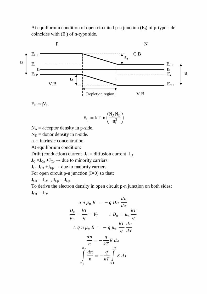
At equilibrium condition of open circuited p-n junction (Ef) of p-type side
coincides with (Ef) of n-type side.
P N
ECP C.B
Ei Ec n
Ef P Ei
V.B Ev n
Depletion region V.B
EB =qVB
EB = kT ln NA ND
ni2
NA = acceptor density in p-side.
ND = donor density in n-side.
ni = intrinsic concentration.
At equilibrium condition:
Drift (conduction) current JC = diffusion current JD
JC =JCn +JCp → due to minority carriers.
JD=JDn +JDp → due to majority carriers.
For open circuit p-n junction (I=0) so that:
JCn= -JDn , JCp= -JDp
To derive the electron density in open circuit p-n junction on both sides:
JCn= -JDn
𝑞 𝑛 𝜇𝑛 𝐸 = − 𝑞 𝐷𝑛 𝑑𝑛
𝑑𝑥
𝐷𝑛𝜇𝑛
=𝑘𝑇
𝑞= 𝑉𝑇 ∴ 𝐷𝑛 = 𝜇𝑛
𝑘𝑇
𝑞
∴ 𝑞 𝑛 𝜇𝑛 𝐸 = − 𝑞 𝜇𝑛 𝑘𝑇
𝑞 𝑑𝑛
𝑑𝑥
𝑑𝑛
𝑛= −
𝑞
𝑘𝑇𝐸 𝑑𝑥
𝑑𝑛
𝑛= −
𝑞
𝑘𝑇
𝑛𝑛
𝑛𝑝
𝐸 𝑑𝑥
𝑥2
𝑥1
EB
EB Eg
Eg EF EF

ln(𝑛) 𝑛𝑛𝑛𝑝
= −𝑞
𝑘𝑇 𝐸 𝑑𝑥
𝑥2
𝑥1
𝑏𝑢𝑡 − 𝐸 𝑑𝑥
𝑥2
𝑥1
= 𝑉𝐵
ln 𝑛𝑛 − ln 𝑛𝑝 =𝑞
𝑘𝑇 𝑉𝐵 𝑜𝑟 ln
𝑛𝑛𝑛𝑝 =
𝑞
𝑘𝑇𝑉𝐵
𝑛𝑛 = 𝑛𝑝 𝑒 𝑞 𝑉𝐵𝑘𝑇
= 𝑛𝑝 𝑒
𝑉𝐵𝑉𝑇
P junction N
VB
X1 X2
Homework:
1- To derive the hole concentration:
𝐽𝐶𝑃 = −𝐽𝐷𝑃 ⇒ 𝑃𝑃 = 𝑃𝑛 𝑒 𝑉𝐵𝑉𝑇
2- Prove that:
𝑉𝐵 =𝑘𝑇
𝑞𝑙𝑛
𝑁𝐷𝑁𝐴
𝑛𝑖2
JDP
JDn
JCP
JCn

8. Diode rectifier action:
8.1. Reverse bias p-n junction:
VB
New potential barrier (VB) = - (VB+V)
IS = reverse current or (saturation current) IC >> ID
IS = ICn +ICp
Both the holes in p-type and electron in n-type (majority carriers) move
away from the junction. Due to large E in the depletion region which is
caused by the new potential barrier (VB'= - (VB +V), the minority carriers
thermally generated will flow and so a reverse saturation current (IS) will
flow. This reverse current will increase with temperature increase since
(e-h) pairs thermally generated will increase, and hence the reverse
resistances of the diode will decrease with temperature increase.
8.2. Forward bias p-n junction:
VB
When V>VB → VD = (V - VB)
I = forward current → ID > IC
= IDp + IDn
8.3. V-I characteristic of diode:

8.4. Current components in a p-n junction:
I = Inp o + Ipn o
𝑛 − 𝑠𝑖𝑑𝑒: I = Inn + Ipn
𝑝 − 𝑠𝑖𝑑𝑒: I = Ipp + Inp
In forward bias, holes diffuse from p to n and electron from n to p. Hole
diffusion current in the n-type decrease exponentially with distance (x).
Similarly for electron in p-type.
To derive the forward current:
The minority hole diffusion current at the junction in n-side is:
Ipn o = −qADP
dp
dx=
qADp
Lp
Pn o − Pno …………………………… 1
Where A= cross sectional area of the diode.
LP= diffusion length for holes.
Lp = Dpτp
τp = mean life time for hole before recombination.
Pno = hole minority thermally generated 𝑛𝑖
2
𝑁𝐷
The forward bias lowers the potential barrier heights which allow more
carriers to cross the junction. Hence Pn o is a function of the forward
voltage V:
Pn o
= Pno e
VVT
………………………………………………………… . . 2
Substitute equation (2) into equation (1) to get:
Ipn o =qADp Pno
Lp e
V
VT − 1 where VT =
kT
q
Similarly the electron current in p-side crossing the junction into p-side:
Inp o =qADn npo
Ln e
V
VT − 1
Hence the total current:
I = Inp o + Ipn o = qA Dn npo
Ln+
Dp Pno
Lp e
V
VT − 1
Diode current equation:
I = −IS e
VVT
− 1 where IS is −ve value
IS = qA Dn npo
Ln+
Dp Pno
Lp
8.5. Diode equation: I
now potential barrier VB′ = VB − V

V= +ve (forward)
V= - ve (reverse)
Minority carrier concentration: V
Pn = Po e −VB
′
VT
, np = nn e −VB
′
VT
I = ID + IS , ID = II = injected current ∝ np + Pn
∴ ID ∝ nn + Pp e −VB
′
VT
= 𝐶 nn + Pp e −VB
′
VT
∴ ID = Be −VB
′
VT
To find B:
For v=0 → I=0 and VB′ = VB
∴ 0 = ID + IS ⇒ ID = −IS
∴ −IS = B e −VB
′
VT
⇒ B = −IS e
VB′
VT
∴ ID = −IS e
VB′
VT
× e −VB
′
VT
= −IS exp VB − VB
′
VT = −IS e
V
VT
I = ID + IS = −IS e
VVT
+ IS = −IS e
V
VT − 1
(- ve) sign means forward is opposite to IS .
At room temperature (T= 300ok):
1
VT=
q
kT= 39 V−1
I = IS e39 V − 1
1- Forward:
V = +ve , and e 39 V
>>> 1
∴ I ≈ IS e39 V
2- Reverse:
V = -ve , and e - 39 V
<<< 1
∴ I ≈ IS

8.6. Load line:
Vi VD RL VR
From KVL: Vi = VD + i RL
The intersection of the load line with the static curve gives the current (i)
corresponding to Vi value. Load line passes through two points:
1- Intersection with x- axis:
i= 0, so that VD = Vi .
2- Intersection with y- axis:
VD =0, i =V i
RL , slope of load line =
∆𝑖
∆𝑉=
1
RL
𝐕𝐢
𝐑𝐋
i
V
i=iD
VD Vi
Q
∆i
∆V
Load line
𝐈 = 𝐈𝐒 𝐞𝟑𝟗 𝐕 − 𝟏
Static ch/s
Operating point

8.7. Linear diode model equivalent circuit:
8.7.1. Forward bias:
8.7.2. Reverse bias:
i
V
Low R1
R1=Rf = 𝑽𝑻
𝑰 ≈ 30 Ω
R1
R2
R2=∞
High
R2
Rf=0
Short circuit
Vγ
Vγ threshold
voltage
Vγ Rf
Not ideal
diode
Vγ ideal
diode
Short circuit
Ideal diode
Vi >> Vγ neglect threshold
voltage
RL
V
i

-V
-i
Rr =∞
Open circuit
Rr ~ 1MΩ
ideal diode
Rr
Not ideal
diode
RL
V

Semiconductor Devices Assistant prof. Dr. Mohammed Adnan Mahdi
1
9. Zener diode:
Zener may have breakdown voltage (Vz) of 2→2oo v depending on doping
level. They are always used in reverse biasing and uses as a voltage
regulator (reference) and constant voltage devices.
Characteristics of Zener diode:
Pz max= max power dissipation.
Pz max= Vz Iz max
Iz max = max current in a Zener diode.
Zener equivalent circuit:
In break down region, Zener diode has small resistance, rz =∆V
∆i change of
Vz with temperature, ∆Vz = ∆T * Vz * Tc
Tc = temperature coefficient.
∆T = change in temperature.
Vz = Zener voltage.
Power dissipation of Zener diode is:
Pz = Vz * Iz
9.1. Zener breakdown:
With heavy doping the depilation layer width becomes narrow, and E across
it is very intense (~ 107 v/m). It is enough to pull electrons out of valence
orbits. Creation of free electrons in this way is called (Zener breakdown),
dominant Vz < 4v.
9.2. Avalanche breakdown:
When the applied reverse voltage reaches breakdown value, minority
carriers in the depletion region are accelerated and reach high enough
velocity to liberate valence electrons from outer orbits. These newly
liberated electrons, further free valence electrons. In this way, avalanche of
p N
-V
-i
ideal
rz =0
rz ≠ 0
Not ideal
Iz
rz Vz Vz
Vz
Ideal zener Practical (not ideal)

Semiconductor Devices Assistant prof. Dr. Mohammed Adnan Mahdi
2
free electrons is obtained. Avalanche occurs for Vz > 6v. Both avalanche
and Zener effects are present between (4 & 6) v.
9.3. Regulation of load current:
I = IL + IZ
R =V−VZ
IL +IZ, IZmin < IZ < IZmax
Q - Point is chosen such that:
Iz = 20 % of Izmax
R =V−VZ
IL +0.2IZmax
RL VL
R
Vz
V Iz
I
IL
-V
Iz min
Iz max
Iz
Vz
Q

Example: draw the output voltage waveform for the following circuit:
Solution:
Case (1): ideal diode Vi >> Vγ
1- Positive half cycle:
Diode is forward (i.e short cct.)
Vo = Vi
2- Negative half cycle:
Diode is reverse bias (i.e open cct.)
Vo = 0.
Case (2): not ideal diode:
1- Positive half cycle:
Diode is forward:
Vo = Vi − Vγ ×RL
RL +Rf
∴ 𝑉𝑜𝑚 = Vi − Vγ ×RL
RL +Rf
2- Negative half cycle:
Diode is reverse bias:
Vo = Vi ×RL
RL +Rr , Rr ≫ RL
Vi
RL
+ve half
_-ve half
Vo
Vi
wt
Vmi
Vm
Vmo
Vo
+ve
half
-ve
half
-ve
half
+ve
half
Vi = Vm sin (wt)
Vi
Vγ Rf ~ 30Ω
RL ~ 1kΩ
Vo
Vo RL
Rr
Vi