331 week13.1spring 2006 14:332:331 computer architecture and assembly language spring 2006 week 13...
Post on 20-Dec-2015
228 views
TRANSCRIPT

331 Week13.1 Spring 2006
14:332:331Computer Architecture and Assembly Language
Spring 2006
Week 13Basics of Cache
[Adapted from Dave Patterson’s UCB CS152 slides and
Mary Jane Irwin’s PSU CSE331 slides]

331 Week13.2 Spring 2006
A question to think about …
Given a pipelined datapath, which instruction may slow down the pipeline the most:
R-type beq j lw sw

331 Week13.3 Spring 2006
Review: Major Components of a Computer
Processor
Control
Datapath
Memory
Devices
Input
Output

331 Week13.4 Spring 2006
SecondLevelCache
(SRAM)
A Typical Memory Hierarchy
Control
Datapath
SecondaryMemory(Disk)
On-Chip Components
RegF
ile
MainMemory(DRAM)
Data
Cache
InstrC
ache
ITLB
DT
LB
eDRAM
Speed (ns): .1’s 1’s 10’s 100’s 1,000’s
Size (bytes): 100’s K’s 10K’s M’s T’s
Cost: highest lowest
By taking advantage of the principle of locality: Present the user with as much memory as is available in the
cheapest technology. Provide access at the speed offered by the fastest technology.

331 Week13.5 Spring 2006
Characteristics of the Memory Hierarchy
Increasing distance from the processor in access time
L1$
L2$
Main Memory
Secondary Memory
Processor
(Relative) size of the memory at each level
Inclusive– what is in L1$ is a subset of what is in L2$ is a subset of what is in MM that is a subset of is in SM
4-8 bytes (word)
1 block
1,023+ bytes (disk sector = page)
8-32 bytes (block)

331 Week13.6 Spring 2006
Why Care About the Memory Hierarchy?
1
10
100
1000
1980
1981
1983
1984
1985
1986
1987
1988
1989
1990
1991
1992
1993
1994
1995
1996
1997
1998
1999
2000
DRAM
CPU19
82
Processor-MemoryPerformance Gap:(grows 50% / year)
Per
form
ance
Time
“Moore’s Law”
Processor-DRAM Memory GapµProc60%/year(2X/1.5yr)
DRAM9%/year(2X/10yrs)

331 Week13.7 Spring 2006
Memory Hierarchy: Goals Fact: Large memories are slow, fast memories are
small
How do we create a memory that gives the illusion of being large, cheap and fast (most of the time)?
by taking advantage of
The Principle of Locality: Programs access a relatively small portion of the address space at any instant of time.
Address Space0 2n - 1
Probabilityof reference
331 Week13.8 Spring 2006
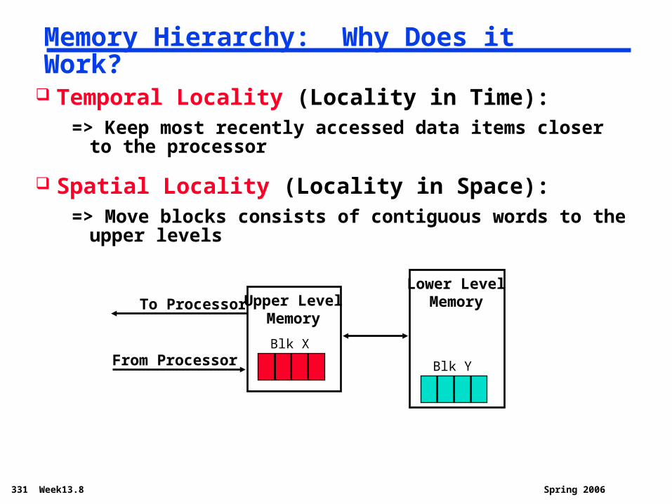
Memory Hierarchy: Why Does it Work?
Temporal Locality (Locality in Time):=> Keep most recently accessed data items closer to the
processor
Spatial Locality (Locality in Space):=> Move blocks consists of contiguous words to the upper
levels
Lower LevelMemoryUpper Level
MemoryTo Processor
From ProcessorBlk X
Blk Y
331 Week13.9 Spring 2006
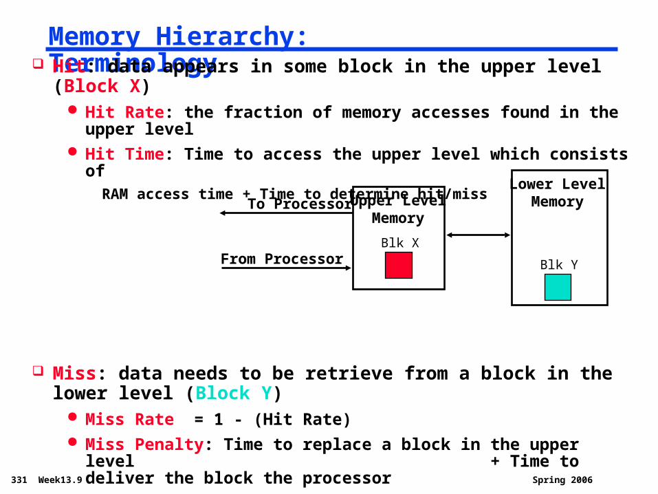
Memory Hierarchy: Terminology Hit: data appears in some block in the upper level (Block X)
Hit Rate: the fraction of memory accesses found in the upper level Hit Time: Time to access the upper level which consists of
RAM access time + Time to determine hit/miss
Miss: data needs to be retrieve from a block in the lower level (Block Y)
Miss Rate = 1 - (Hit Rate) Miss Penalty: Time to replace a block in the upper level
+ Time to deliver the block the processor Hit Time << Miss Penalty
Lower LevelMemoryUpper Level
MemoryTo Processor
From ProcessorBlk X
Blk Y

331 Week13.10 Spring 2006
How is the Hierarchy Managed? registers <-> memory
by compiler (programmer?)
cache <-> main memory by the hardware
main memory <-> disks by the hardware and operating system (virtual memory) by the programmer (files)

331 Week13.11 Spring 2006
Two questions to answer (in hardware): Q1: How do we know if a data item is in the cache? Q2: If it is, how do we find it?
First method: Direct mapped
- For each item of data at the lower level, there is exactly one location in the cache where it might be (i.e., lots of items at the lower level share locations in the upper level)
Block size is one word of data Mapping: (word address) modulo (# of words in the
cache)
Cache

331 Week13.12 Spring 2006
Caching: A Simple First Example
00
011011
Cache0000000100100011010001010110011110001001101010111100110111101111
Main Memory
Q2: How do we find it?
Use low order 2 memory address bits to determine which cache block (i.e., modulo the number of blocks in the cache)
Tag Data
Q1: Is it there?
Compare the cache tag to the high order 2 memory address bits to tell if the memory block is in the cache
Valid
331 Week13.13 Spring 2006
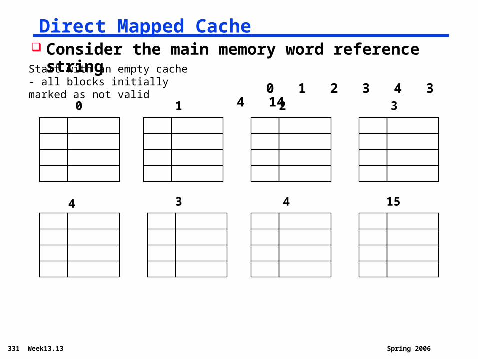
Direct Mapped Cache
0 1 2 3
4 3 4 15
Consider the main memory word reference string 0 1 2 3 4 3 4 14Start with an empty cache - all
blocks initially marked as not valid

331 Week13.14 Spring 2006
Another Reference String Mapping
0 4 0 4
0 4 0 4
Consider the main memory word reference string 0 4 0 4 0 4 0 4Start with an empty cache - all
blocks initially marked as not valid

331 Week13.15 Spring 2006
Sources of Cache Misses Compulsory (cold start or process migration, first
reference): first access to a block “Cold” fact of life, not a whole lot you can do about it If you are going to run “billions” of instruction,
Compulsory Misses are insignificant
Conflict (collision): Multiple memory locations mapped to the same cache
location Solution 1: increase cache size Solution 2: increase associativity
Capacity: Cache cannot contain all blocks accessed by the program Solution: increase cache size

331 Week13.16 Spring 2006
One word/block, cache size = 1K wordsMIPS Direct Mapped Cache Example
Hit 20Tag 10Index
DataIndex TagValid012...
102110221023
31 30 . . . 13 12 11 . . . 2 1 0
Byte offset
20
Data
32

331 Week13.17 Spring 2006
Multiword Block Direct Mapped Cache
8Index
DataIndex TagValid012...
253254255
31 30 . . . 13 12 11 . . . 4 3 2 1 0Byte offset
20
20Tag
Hit Data
32
Block offset
Four words/block, cache size = 1K words
What kind of locality are we taking advantage of?

331 Week13.18 Spring 2006
Taking Advantage of Spatial Locality
0
Let cache block hold more than one word 0 1 2 3 4 3 4 15
1 2
3 4 3
4 15
Start with an empty cache - all blocks initially marked as not valid

331 Week13.19 Spring 2006
Reducing Cache Miss Rates #1
1. Allow more flexible block placement
In a direct mapped cache a memory block maps to exactly one cache block
At the other extreme, could allow a memory block to be mapped to any cache block – fully associative cache
A compromise is to divide the cache into sets each of which consists of n “ways” (n-way set associative). A memory block maps to a unique set (specified by the index field) and can be placed in any way of that set (so there are n choices)
(block address) modulo (# sets in the cache)

331 Week13.20 Spring 2006
Set Associative Cache Example
0
Cache
Main Memory
Q2: How do we find it?
Use next 1 low order memory address bit to determine which cache set (i.e., modulo the number of sets in the cache)
Tag Data
Q1: Is it there?
Compare all the cache tags in the set to the high order 3 memory address bits to tell if the memory block is in the cache
V
0000xx0001xx0010xx0011xx0100xx0101xx0110xx0111xx1000xx1001xx1010xx1011xx1100xx1101xx1110xx1111xx
Two low order bits define the byte in the word (32-b words)One word blocks
Set
1
01
Way
0
1

331 Week13.21 Spring 2006
Another Reference String Mapping
0 4 0 4
Consider the main memory word reference string 0 4 0 4 0 4 0 4Start with an empty cache - all
blocks initially marked as not valid

331 Week13.22 Spring 2006
Four-Way Set Associative Cache 28 = 256 sets each with four ways (each with one
block) 31 30 . . . 13 12 11 . . . 2 1 0 Byte offset
DataTagV012...
253 254 255
DataTagV012...
253 254 255
DataTagV012...
253 254 255
Index DataTagV012...
253 254 255
8Index
22Tag
Hit Data
32
4x1 select

331 Week13.23 Spring 2006
Range of Set Associative Caches For a fixed size cache, each increase by a factor of
two in associativity doubles the number of blocks per set (i.e., the number or ways) and halves the number of sets – decreases the size of the index by 1 bit and increases the size of the tag by 1 bit
Block offset Byte offsetIndexTag
Decreasing associativity
Fully associative(only one set)Tag is all the bits exceptblock and byte offset
Direct mapped(only one way)Smaller tags
Increasing associativity
Selects the setUsed for tag compare Selects the word in the block

331 Week13.24 Spring 2006
Announcement
HW 5
Notes and updated Syllabus will be put online today afternoon
No lecture on Friday

331 Week13.25 Spring 2006
Handling Cache Misses
Handling hit is trivial
Handling misses needs to stall the processor
Upon an instruction cache miss Send the original PC value (current PC – 4) to the
memory Instruct main memory to perform a read and wait for the
memory to complete its access Write the cache entry, putting the data from memory in
the data portion of the entry, writing the upper bits of the address (from the ALU) into the tag field, and turning the valid bit on
Restart the instruction execution at the first step, which will re-fetch the instruction, this time finding it in the cache
Similar for data cache miss

331 Week13.26 Spring 2006
Handling Writes
The cache and memory are inconsistent when their values (of the same data) are different
A simple solution: write through Write to both the cache and the memory at the same time Poor performance. Every store instruction needs to stall
the processor (a memory access can take 100 CPU cycles)
Alternative: write back Write to the cache; write to the memory when the cache
block is replaced later.

331 Week13.27 Spring 2006
Cache Summary The Principle of Locality:
Program likely to access a relatively small portion of the address space at any instant of time
- Temporal Locality: Locality in Time
- Spatial Locality: Locality in Space
Three Major Categories of Cache Misses: Compulsory Misses: sad facts of life. Example: cold start
misses Conflict Misses: increase cache size and/or associativity
Nightmare Scenario: ping pong effect! Capacity Misses: increase cache size
Cache Design Space total size, block size, associativity (replacement policy) write-hit policy (write-through, write-back) write-miss policy (write allocate, write buffers)

331 Week13.28 Spring 2006
The off-chip interconnect and memory architecture can affect overall system performance in dramatic ways.
Memory Systems that Support Caches
CPU
Cache
Memory
bus
One word wide organization (one word wide bus and one word wide memory) Assume
1. 1 clock cycle (2 ns) to send the address
2. 25 clock cycles (50 ns) for DRAM cycle time, 8 clock cycles (16 ns) access time
3. 1 clock cycle (2ns) to return a word of data
Memory-Bus to Cache bandwidth
number of bytes accessed from memory and transferred to cache/CPU per clock cycle
32-bit data&
32-bit addrper cycle
on-chip

331 Week13.29 Spring 2006
One Word Wide Memory Organization
CPU
Cache
Memory
bus
on-chip
If the block size is one word, then for a memory access due to a cache miss, the pipeline will have to stall the number of cycles required to return one data word from memory
cycle to send address
cycles to read DRAM
cycle to return data
total clock cycles miss penalty
Number of bytes transferred per clock cycle (bandwidth) for a single miss is
bytes per clock
1
25
1
27
4/27 = 0.148

331 Week13.30 Spring 2006
One Word Wide Memory Organization, con’t
CPU
Cache
Memory
bus
on-chip
What if the block size is four words? cycle to send 1st address
cycles to read DRAM
cycles to return last data word
total clock cycles miss penalty
Number of bytes transferred per clock cycle (bandwidth) for a single miss is
bytes per clock
25 cycles
25 cycles
25 cycles
25 cycles
1
4 x 25 = 100
1
102
(4 x 4)/102 = 0.157

331 Week13.31 Spring 2006
Interleaved Memory Organization
For a block size of four words cycle to send 1st address
cycles to read DRAM
cycles to return last data word
total clock cycles miss penalty
CPU
Cache
Memorybank 1
bus
on-chip
Memorybank 0
Memorybank 2
Memorybank 3
Number of bytes transferred per clock cycle (bandwidth) for a single miss is
bytes per clock
25 cycles
25 cycles
25 cycles
25 cycles
(4 x 4)/30 = 0.533
1
25 + 3 = 28
1
30

331 Week13.32 Spring 2006
DRAM Memory System Summary
Its important to match the cache characteristics caches access one block at a time (usually more than
one word)
with the DRAM characteristics use DRAMs that support fast multiple word accesses,
preferably ones that match the block size of the cache
with the memory-bus characteristics make sure the memory-bus can support the DRAM
access rates and patterns with the goal of increasing the Memory-Bus to Cache
bandwidth