34.particledetectors ataccelerators -...
TRANSCRIPT

34. Detectors at accelerators 1
34. PARTICLE DETECTORS
AT ACCELERATORS
Revised 2015. See the various sections for authors.
34.1. Introduction
This review summarizes the detector technologies employed at accelerator particlephysics experiments. Several of these detectors are also used in a non-accelerator contextand examples of such applications will be provided. The detector techniques which arespecific to non-accelerator particle physics experiments are the subject of Chap. 35. Moredetailed discussions of detectors and their underlying physics can be found in books byFerbel [1], Kleinknecht [2], Knoll [3], Green [4], Leroy & Rancoita [5], and Grupen [6].
In Table 34.1 are given typical resolutions and deadtimes of common charged particledetectors. The quoted numbers are usually based on typical devices, and should beregarded only as rough approximations for new designs. The spatial resolution refers tothe intrinsic detector resolution, i.e. without multiple scattering. We note that analogdetector readout can provide better spatial resolution than digital readout by measuringthe deposited charge in neighboring channels. Quoted ranges attempt to be representativeof both possibilities. The time resolution is defined by how accurately the time atwhich a particle crossed the detector can be determined. The deadtime is the minimumseparation in time between two resolved hits on the same channel. Typical performanceof calorimetry and particle identification are provided in the relevant sections below.
Table 34.1: Typical resolutions and deadtimes of common charged particledetectors. Revised November 2011.
Intrinsinc Spatial Time Dead
Detector Type Resolution (rms) Resolution Time
Resistive plate chamber . 10 mm 1 ns (50 psa) —
Streamer chamber 300 µmb 2 µs 100 ms
Liquid argon drift [7] ∼175–450 µm ∼ 200 ns ∼ 2 µs
Scintillation tracker ∼100 µm 100 ps/nc 10 ns
Bubble chamber 10–150 µm 1 ms 50 msd
Proportional chamber 50–100 µme 2 ns 20-200 ns
Drift chamber 50–100 µm 2 nsf 20-100 ns
Micro-pattern gas detectors 30–40 µm < 10 ns 10-100 ns
Silicon strip pitch/(3 to 7)g few nsh . 50 nsh
Silicon pixel . 10 µm few nsh . 50 nsh
Emulsion 1 µm — —
a For multiple-gap RPCs.b 300 µm is for 1 mm pitch (wirespacing/
√12).
c n = index of refraction.
C. Patrignani et al. (Particle Data Group), Chin. Phys. C, 40, 100001 (2016)October 6, 2016 12:10

2 34. Detectors at accelerators
d Multiple pulsing time.e Delay line cathode readout can give ±150 µm parallel to anode wire.f For two chambers.g The highest resolution (“7”) is obtained for small-pitch detectors ( . 25 µm) with
pulse-height-weighted center finding.h Limited by the readout electronics [8].
34.2. Photon detectors
Updated August 2011 by D. Chakraborty (Northern Illinois U) and T. Sumiyoshi (TokyoMetro U).
Most detectors in high-energy, nuclear, and astrophysics rely on the detection ofphotons in or near the visible range, 100 nm .λ . 1000 nm, or E ≈ a few eV. Thisrange covers scintillation and Cherenkov radiation as well as the light detected in manyastronomical observations.
Generally, photodetection involves generating a detectable electrical signal proportionalto the (usually very small) number of incident photons. The process involves three distinctsteps:1. generation of a primary photoelectron or electron-hole (e-h) pair by an incident photon
by the photoelectric or photoconductive effect,2. amplification of the p.e. signal to detectable levels by one or more multiplicative
bombardment steps and/or an avalanche process (usually), and,3. collection of the secondary electrons to form the electrical signal.
The important characteristics of a photodetector include the following in statisticalaverages:1. quantum efficiency (QE or ǫQ): the number of primary photoelectrons generated per
incident photon (0 ≤ ǫQ ≤ 1; in silicon more than one e-h pair per incident photon canbe generated for λ <∼ 165 nm),
2. collection efficiency (CE or ǫC ): the overall acceptance factor other than the generationof photoelectrons (0 ≤ ǫC ≤ 1),
3. gain (G): the number of electrons collected for each photoelectron generated,4. dark current or dark noise: the electrical signal when there is no photon,5. energy resolution: electronic noise (ENC or Ne) and statistical fluctuations in the
amplification process compound the Poisson distribution of nγ photons from a givensource:
σ(E)
〈E〉 =
√
fN
nγǫQǫC+
(
Ne
GnγǫQǫC
)2, (34.1)
where fN , or the excess noise factor (ENF), is the contribution to the energydistribution variance due to amplification statistics [9],
6. dynamic range: the maximum signal available from the detector (this is usuallyexpressed in units of the response to noise-equivalent power, or NEP, which is theoptical input power that produces a signal-to-noise ratio of 1),
7. time dependence of the response: this includes the transit time, which is the timebetween the arrival of the photon and the electrical pulse, and the transit time spread,
October 6, 2016 12:10

34. Detectors at accelerators 3
which contributes to the pulse rise time and width, and8. rate capability: inversely proportional to the time needed, after the arrival of one
photon, to get ready to receive the next.
Table 34.2: Representative characteristics of some photodetectors commonly used inparticle physics. The time resolution of the devices listed here vary in the 10–2000 psrange.
Type λ ǫQ ǫC Gain Risetime Area 1-p.e noise HV Price
(nm) (ns) (mm2) (Hz) (V) (USD)
PMT∗ 115–1700 0.15–0.25 103–107 0.7–10 102–105 10–104 500–3000 100–5000
MCP∗ 100–650 0.01–0.10 103–107 0.15–0.3 102–104 0.1–200 500–3500 10–6000
HPD∗ 115–850 0.1–0.3 103–104 7 102–105 10–103 ∼2 × 10⁴ ∼600
GPM∗ 115–500 0.15–0.3 103–106 O(0.1) O(10) 10–103 300–2000 O(10)
APD 300–1700 ∼0.7 10–108 O(1) 10–103 1–103 400–1400 O(100)
PPD 320–900 0.15–0.3 105–106 ∼ 1 1–10 O(106) 30–60 O(100)
VLPC 500–600 ∼0.9 ∼5 × 10⁴ ∼ 10 1 O(104) ∼7 ∼1
∗These devices often come in multi-anode configurations. In such cases, area, noise, andprice are to be considered on a “per readout-channel” basis.
The QE is a strong function of the photon wavelength (λ), and is usually quoted atmaximum, together with a range of λ where the QE is comparable to its maximum.Spatial uniformity and linearity with respect to the number of photons are highlydesirable in a photodetector’s response.
Optimization of these factors involves many trade-offs and vary widely betweenapplications. For example, while a large gain is desirable, attempts to increase the gainfor a given device also increases the ENF and after-pulsing (“echos” of the main pulse).In solid-state devices, a higher QE often requires a compromise in the timing properties.In other types, coverage of large areas by focusing increases the transit time spread.
Other important considerations also are highly application-specific. These include thephoton flux and wavelength range, the total area to be covered and the efficiency required,the volume available to accommodate the detectors, characteristics of the environmentsuch as chemical composition, temperature, magnetic field, ambient background, as wellas ambient radiation of different types and, mode of operation (continuous or triggered),bias (high-voltage) requirements, power consumption, calibration needs, aging, cost, andso on. Several technologies employing different phenomena for the three steps describedabove, and many variants within each, offer a wide range of solutions to choose from. Thesalient features of the main technologies and the common variants are described below.Some key characteristics are summarized in Table 34.2.
October 6, 2016 12:10
4 34. Detectors at accelerators
34.2.1. Vacuum photodetectors : Vacuum photodetectors can be broadly subdividedinto three types: photomultiplier tubes, microchannel plates, and hybrid photodetectors.
34.2.1.1. Photomultiplier tubes: A versatile class of photon detectors, vacuumphotomultiplier tubes (PMT) has been employed by a vast majority of all particle physicsexperiments to date [9]. Both “transmission-” and “reflection-type” PMT’s are widelyused. In the former, the photocathode material is deposited on the inside of a transparentwindow through which the photons enter, while in the latter, the photocathode materialrests on a separate surface that the incident photons strike. The cathode material hasa low work function, chosen for the wavelength band of interest. When a photon hitsthe cathode and liberates an electron (the photoelectric effect), the latter is acceleratedand guided by electric fields to impinge on a secondary-emission electrode, or dynode,which then emits a few (∼ 5) secondary electrons. The multiplication process is repeatedtypically 10 times in series to generate a sufficient number of electrons, which are collectedat the anode for delivery to the external circuit. The total gain of a PMT depends onthe applied high voltage V as G = AV kn, where k ≈ 0.7–0.8 (depending on the dynodematerial), n is the number of dynodes in the chain, and A a constant (which also dependson n). Typically, G is in the range of 105–106. Pulse risetimes are usually in the fewnanosecond range. With e.g. two-level discrimination the effective time resolution can bemuch better.
A large variety of PMT’s, including many just recently developed, covers a wide spanof wavelength ranges from infrared (IR) to extreme ultraviolet (XUV) [10]. They arecategorized by the window materials, photocathode materials, dynode structures, anodeconfigurations, etc. Common window materials are borosilicate glass for IR to near-UV,fused quartz and sapphire (Al2O3) for UV, and MgF2 or LiF for XUV. The choiceof photocathode materials include a variety of mostly Cs- and/or Sb-based compoundssuch as CsI, CsTe, bi-alkali (SbRbCs, SbKCs), multi-alkali (SbNa2KCs), GaAs(Cs),GaAsP, etc. Sensitive wavelengths and peak quantum efficiencies for these materials aresummarized in Table 34.3. Typical dynode structures used in PMT’s are circular cage,line focusing, box and grid, venetian blind, and fine mesh. In some cases, limited spatialresolution can be obtained by using a mosaic of multiple anodes. Fast PMT’s with verylarge windows—measuring up to 508 mm across—have been developed in recent yearsfor detection of Cherenkov radiation in neutrino experiments such as Super-Kamiokandeand KamLAND among many others. Specially prepared low-radioactivity glass is usedto make these PMT’s, and they are also able to withstand the high pressure of thesurrounding liquid.
PMT’s are vulnerable to magnetic fields—sometimes even the geomagnetic field causeslarge orientation-dependent gain changes. A high-permeability metal shield is oftennecessary. However, proximity-focused PMT’s, e.g. the fine-mesh types, can be usedeven in a high magnetic field (≥ 1 T) if the electron drift direction is parallel to thefield. CMS uses custom-made vacuum phototriodes (VPT) mounted on the back face ofprojective lead tungstate crystals to detect scintillation light in the endcap sections of itselectromagnetic calorimeters, which are inside a 3.8 T superconducting solenoid. A VPTemploys a single dynode (thus, G ≈ 10) placed close to the photocathode, and a meshanode plane between the two, to help it cope with the strong magnetic field, which is not
October 6, 2016 12:10

34. Detectors at accelerators 5
too unfavorably oriented with respect to the photodetector axis in the endcaps (within25), but where the radiation level is too high for Avalanche Photodiodes (APD’s) likethose used in the barrel section.
34.2.1.2. Microchannel plates: A typical Microchannel plate (MCP) photodetectorconsists of one or more ∼2 mm thick glass plates with densely packed O(10 µm)-diametercylindrical holes, or “channels”, sitting between the transmission-type photocathodeand anode planes, separated by O(1 mm) gaps. Instead of discrete dynodes, the innersurface of each cylindrical tube serves as a continuous dynode for the entire cascadeof multiplicative bombardments initiated by a photoelectron. Gain fluctuations can beminimized by operating in a saturation mode, whence each channel is only capable of abinary output, but the sum of all channel outputs remains proportional to the number ofphotons received so long as the photon flux is low enough to ensure that the probabilityof a single channel receiving more than one photon during a single time gate is negligible.MCP’s are thin, offer good spatial resolution, have excellent time resolution (∼20 ps), andcan tolerate random magnetic fields up to 0.1 T and axial fields up to ∼ 1 T. However,they suffer from relatively long recovery time per channel and short lifetime. MCP’s arewidely employed as image-intensifiers, although not so much in HEP or astrophysics.
34.2.1.3. Hybrid photon detectors: Hybrid photon detectors (HPD) combine thesensitivity of a vacuum PMT with the excellent spatial and energy resolutions of a Sisensor [11]. A single photoelectron ejected from the photocathode is accelerated througha potential difference of ∼20 kV before it impinges on the silicon sensor/anode. The gainnearly equals the maximum number of e-h pairs that could be created from the entirekinetic energy of the accelerated electron: G ≈ eV/w, where e is the electronic charge,V is the applied potential difference, and w ≈ 3.7 eV is the mean energy required tocreate an e-h pair in Si at room temperature. Since the gain is achieved in a single step,one might expect to have the excellent resolution of a simple Poisson statistic with largemean, but in fact it is even better, thanks to the Fano effect discussed in Sec. 34.7.
Low-noise electronics must be used to read out HPD’s if one intends to take advantageof the low fluctuations in gain, e.g. when counting small numbers of photons. HPD’s canhave the same ǫQ ǫC and window geometries as PMT’s and can be segmented down to∼50 µm. However, they require rather high biases and will not function in a magneticfield. The exception is proximity-focused devices (⇒ no (de)magnification) in an axialfield. With time resolutions of ∼10 ps and superior rate capability, proximity-focusedHPD’s can be an alternative to MCP’s. Current applications of HPD’s include theCMS hadronic calorimeter and the RICH detector in LHCb. Large-size HPD’s withsophisticated focusing may be suitable for future water Cherenkov experiments.
Hybrid APD’s (HAPD’s) add an avalanche multiplication step following the electronbombardment to boost the gain by a factor of ∼50. This affords a higher gain and/orlower electrical bias, but also degrades the signal definition.
October 6, 2016 12:10

6 34. Detectors at accelerators
Table 34.3: Properties of photocathode and window materials commonly used invacuum photodetectors [10].
Photocathode λ Window Peak ǫQ (λ/nm)
material (nm) material
CsI 115–200 MgF2 0.11 (140)
CsTe 115–320 MgF2 0.14 (240)
Bi-alkali 300–650 Borosilicate 0.27 (390)
160-650 Synthetic Silica 0.27 (390)
“Ultra Bi-alkali” 300–650 Borosilicate 0.43 (350)
160-650 Synthetic Silica 0.43 (350)
Multi-alkali 300–850 Borosilicate 0.20 (360)
160-850 Synthetic Silica 0.20 (360)
GaAs(Cs)∗ 160–930 Synthetic Silica 0.23 (280)
GaAsP(Cs) 300-750 Borosilicate 0.50 (500)
InP/InGaAsP† 350-1700 Borosilicate 0.01 (1100)
∗Reflection type photocathode is used. †Requires cooling to ∼ −80C.
34.2.2. Gaseous photon detectors : In gaseous photomultipliers (GPM) a photoelec-tron in a suitable gas mixture initiates an avalanche in a high-field region, producing alarge number of secondary impact-ionization electrons. In principle the charge multiplica-tion and collection processes are identical to those employed in gaseous tracking detectorssuch as multiwire proportional chambers, micromesh gaseous detectors (Micromegas), orgas electron multipliers (GEM). These are discussed in Sec. 34.6.4.
The devices can be divided into two types depending on the photocathode material.One type uses solid photocathode materials much in the same way as PMT’s. Since it isresistant to gas mixtures typically used in tracking chambers, CsI is a common choice.In the other type, photoionization occurs on suitable molecules vaporized and mixed inthe drift volume. Most gases have photoionization work functions in excess of 10 eV,which would limit their sensitivity to wavelengths far too short. However, vapors ofTMAE (tetrakis dimethyl-amine ethylene) or TEA (tri-ethyl-amine), which have smallerwork functions (5.3 eV for TMAE and 7.5 eV for TEA), are suited for XUV photondetection [12]. Since devices like GEM’s offer sub-mm spatial resolution, GPM’s areoften used as position-sensitive photon detectors. They can be made into flat panelsto cover large areas (O(1 m2)), can operate in high magnetic fields, and are relativelyinexpensive. Many of the ring imaging Cherenkov (RICH) detectors to date have usedGPM’s for the detection of Cherenkov light [13]. Special care must be taken to suppressthe photon-feedback process in GPM’s. It is also important to maintain high purity ofthe gas as minute traces of O2 can significantly degrade the detection efficiency.
October 6, 2016 12:10

34. Detectors at accelerators 7
34.2.3. Solid-state photon detectors : In a phase of rapid development, solid-statephotodetectors are competing with vacuum- or gas-based devices for many existingapplications and making way for a multitude of new ones. Compared to traditionalvacuum- and gaseous photodetectors, solid-state devices are more compact, lightweight,rugged, tolerant to magnetic fields, and often cheaper. They also allow fine pixelization,are easy to integrate into large systems, and can operate at low electric potentials, whilematching or exceeding most performance criteria. They are particularly well suited fordetection of γ- and X-rays. Except for applications where coverage of very large areasor dynamic range is required, solid-state detectors are proving to be the better choice.Some hybrid devices attempt to combine the best features of different technologies whileapplications of nanotechnology are opening up exciting new possibilities.
Silicon photodiodes (PD) are widely used in high-energy physics as particle detectorsand in a great number of applications (including solar cells!) as light detectors. Thestructure is discussed in some detail in Sec. 34.7. In its simplest form, the PD is areverse-biased p-n junction. Photons with energies above the indirect bandgap energy(wavelengths shorter than about 1050 nm, depending on the temperature) can create e-hpairs (the photoconductive effect), which are collected on the p and n sides, respectively.Often, as in the PD’s used for crystal scintillator readout in CLEO, L3, Belle, BaBar,and GLAST, intrinsic silicon is doped to create a p-i-n structure. The reverse biasincreases the thickness of the depleted region; in the case of these particular detectors,to full depletion at a depth of about 100 µm. Increasing the depletion depth decreasesthe capacitance (and hence electronic noise) and extends the red response. Quantumefficiency can exceed 90%, but falls toward the red because of the increasing absorptionlength of light in silicon. The absorption length reaches 100 µm at 985 nm. However,since G = 1, amplification is necessary. Optimal low-noise amplifiers are slow, but, evenso, noise limits the minimum detectable signal in room-temperature devices to severalhundred photons.
Very large arrays containing O(107) of O(10 µm2)-sized photodiodes pixelizing aplane are widely used to photograph all sorts of things from everyday subjects at visiblewavelengths to crystal structures with X-rays and astronomical objects from infrared toUV. To limit the number of readout channels, these are made into charge-coupled devices(CCD), where pixel-to-pixel signal transfer takes place over thousands of synchronouscycles with sequential output through shift registers [14]. Thus, high spatial resolutionis achieved at the expense of speed and timing precision. Custom-made CCD’s havevirtually replaced photographic plates and other imagers for astronomy and in spacecraft.Typical QE’s exceed 90% over much of the visible spectrum, and “thick” CCD’s haveuseful QE up to λ = 1 µm. Active Pixel Sensor (APS) arrays with a preamplifier oneach pixel and CMOS processing afford higher speeds, but are challenged at longerwavelengths. Much R&D is underway to overcome the limitations of both CCD andCMOS imagers.
In APD’s, an exponential cascade of impact ionizations initiated by the originalphotogenerated e-h pair under a large reverse-bias voltage leads to an avalanchebreakdown [15]. As a result, detectable electrical response can be obtained from low-intensity optical signals down to single photons. Excellent junction uniformity is critical,
October 6, 2016 12:10

8 34. Detectors at accelerators
and a guard ring is generally used as a protection against edge breakdown. Well-designedAPD’s, such as those used in CMS’ crystal-based electromagnetic calorimeter, haveachieved ǫQ ǫC ≈ 0.7 with sub-ns response time. The sensitive wavelength window andgain depend on the semiconductor used. The gain is typically 10–200 in linear and upto 108 in Geiger mode of operation. Stability and close monitoring of the operatingtemperature are important for linear-mode operation, and substantial cooling is oftennecessary. Position-sensitive APD’s use time information at multiple anodes to calculatethe hit position.
One of the most promising recent developments in the field is that of devices consistingof large arrays (O(103)) of tiny APD’s packed over a small area (O(1 mm2)) andoperated in a limited Geiger mode [16]. Among different names used for this classof photodetectors, “PPD” (for “Pixelized Photon Detector”) is most widely accepted(formerly “SiPM”). Although each cell only offers a binary output, linearity with respectto the number of photons is achieved by summing the cell outputs in the same way as witha MCP in saturation mode (see above). PPD’s are being adopted as the preferred solutionfor various purposes including medical imaging, e.g. positron emission tomography (PET).These compact, rugged, and economical devices allow auto-calibration through decentseparation of photoelectron peaks and offer gains of O(106) at a moderate bias voltage(∼50 V). However, the single-photoelectron noise of a PPD, being the logical “or” ofO(103) Geiger APD’s, is rather large: O(1 MHz/mm2) at room temperature. PPD’s areparticularly well-suited for applications where triggered pulses of several photons areexpected over a small area, e.g. fiber-guided scintillation light. Intense R&D is expectedto lower the noise level and improve radiation hardness, resulting in coverage of largerareas and wider applications. Attempts are being made to combine the fabrication of thesensors and the front-end electronics (ASIC) in the same process with the goal of makingPPD’s and other finely pixelized solid-state photodetectors extremely easy to use.
Of late, much R&D has been directed to p-i-n diode arrays based on thin polycrystallinediamond films formed by chemical vapor deposition (CVD) on a hot substrate (∼1000K) from a hydrocarbon-containing gas mixture under low pressure (∼100 mbar).These devices have maximum sensitivity in the extreme- to moderate-UV region [17].Many desirable characteristics, including high tolerance to radiation and temperaturefluctuations, low dark noise, blindness to most of the solar radiation spectrum, andrelatively low cost make them ideal for space-based UV/XUV astronomy, measurement ofsynchrotron radiation, and luminosity monitoring at (future) lepton collider(s).
Visible-light photon counters (VLPC) utilize the formation of an impurity band only50 meV below the conduction band in As-doped Si to generate strong (G ≈ 5 × 10⁴)yet sharp response to single photons with ǫQ ≈ 0.9 [18]. The smallness of the bandgap considerably reduces the gain dispersion. Only a very small bias (∼7 V) is needed,but high sensitivity to infrared photons requires cooling below 10 K. The dark noiseincreases sharply and exponentially with both temperature and bias. The Run 2 DØdetector used 86000 VLPC’s to read the optical signal from its scintillating-fiber trackerand scintillator-strip preshower detectors.
October 6, 2016 12:10

34. Detectors at accelerators 9
34.3. Organic scintillators
Revised August 2011 by Kurtis F. Johnson (FSU).
Organic scintillators are broadly classed into three types, crystalline, liquid, and plastic,all of which utilize the ionization produced by charged particles (see Sec. 33.2 of thisReview) to generate optical photons, usually in the blue to green wavelength regions [19].Plastic scintillators are by far the most widely used, liquid organic scintillator is findingincreased use, and crystal organic scintillators are practically unused in high-energyphysics. Plastic scintillator densities range from 1.03 to 1.20 g cm−3. Typical photonyields are about 1 photon per 100 eV of energy deposit [20]. A one-cm-thick scintillatortraversed by a minimum-ionizing particle will therefore yield ≈ 2 × 10⁴ photons. Theresulting photoelectron signal will depend on the collection and transport efficiency of theoptical package and the quantum efficiency of the photodetector.
Organic scintillator does not respond linearly to the ionization density. Very denseionization columns emit less light than expected on the basis of dE/dx for minimum-ionizing particles. A widely used semi-empirical model by Birks posits that recombinationand quenching effects between the excited molecules reduce the light yield [21]. Theseeffects are more pronounced the greater the density of the excited molecules. Birks’formula is
dL
dx= L0
dE/dx
1 + kB dE/dx, (34.2)
where L is the luminescence, L0 is the luminescence at low specific ionization density,and kB is Birks’ constant, which must be determined for each scintillator by measurement.Decay times are in the ns range; rise times are much faster. The high light yield andfast response time allow the possibility of sub-ns timing resolution [22]. The fraction oflight emitted during the decay “tail” can depend on the exciting particle. This allowspulse shape discrimination as a technique to carry out particle identification. Because ofthe hydrogen content (carbon to hydrogen ratio ≈ 1) plastic scintillator is sensitive toproton recoils from neutrons. Ease of fabrication into desired shapes and low cost hasmade plastic scintillator a common detector element. In the form of scintillating fiber ithas found widespread use in tracking and calorimetry [23].
Demand for large volume detectors has lead to increased use of liquid organicscintillator, which has the same scintillation mechanism as plastic scintillator, due to itscost advantage. The containment vessel defines the detector shape; photodetectors orwaveshifters may be immersed in the liquid.
34.3.1. Scintillation mechanism :
A charged particle traversing matter leaves behind it a wake of excited molecules.Certain types of molecules, however, will release a small fraction (≈ 3%) of this energyas optical photons. This process, scintillation, is especially marked in those organicsubstances which contain aromatic rings, such as polystyrene (PS) and polyvinyltoluene(PVT). Liquids which scintillate include toluene, xylene and pseudocumene.
In fluorescence, the initial excitation takes place via the absorption of a photon,and de-excitation by emission of a longer wavelength photon. Fluors are used as“waveshifters” to shift scintillation light to a more convenient wavelength. Occurring
October 6, 2016 12:10
10 34. Detectors at accelerators
in complex molecules, the absorption and emission are spread out over a wide band ofphoton energies, and have some overlap, that is, there is some fraction of the emittedlight which can be re-absorbed [24]. This “self-absorption” is undesirable for detectorapplications because it causes a shortened attenuation length. The wavelength differencebetween the major absorption and emission peaks is called the Stokes’ shift. It is usuallythe case that the greater the Stokes’ shift, the smaller the self absorption thus, a largeStokes’ shift is a desirable property for a fluor.
Ionization excitation of base plastic
Forster energy transfer
γ
γ
base plastic
primary fluor (~1% wt/wt )
secondary fluor (~0.05% wt/wt )
photodetector
emit UV, ~340 nm
absorb blue photon
absorb UV photon
emit blue, ~400 nm
1 m
10−4m
10−8m
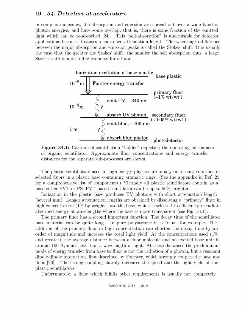
Figure 34.1: Cartoon of scintillation “ladder” depicting the operating mechanismof organic scintillator. Approximate fluor concentrations and energy transferdistances for the separate sub-processes are shown.
The plastic scintillators used in high-energy physics are binary or ternary solutions ofselected fluors in a plastic base containing aromatic rings. (See the appendix in Ref. 25for a comprehensive list of components.) Virtually all plastic scintillators contain as abase either PVT or PS. PVT-based scintillator can be up to 50% brighter.
Ionization in the plastic base produces UV photons with short attenuation length(several mm). Longer attenuation lengths are obtained by dissolving a “primary” fluor inhigh concentration (1% by weight) into the base, which is selected to efficiently re-radiateabsorbed energy at wavelengths where the base is more transparent (see Fig. 34.1).
The primary fluor has a second important function. The decay time of the scintillatorbase material can be quite long – in pure polystyrene it is 16 ns, for example. Theaddition of the primary fluor in high concentration can shorten the decay time by anorder of magnitude and increase the total light yield. At the concentrations used (1%and greater), the average distance between a fluor molecule and an excited base unit isaround 100 A, much less than a wavelength of light. At these distances the predominantmode of energy transfer from base to fluor is not the radiation of a photon, but a resonantdipole-dipole interaction, first described by Foerster, which strongly couples the base andfluor [26]. The strong coupling sharply increases the speed and the light yield of theplastic scintillators.
Unfortunately, a fluor which fulfills other requirements is usually not completely
October 6, 2016 12:10

34. Detectors at accelerators 11
adequate with respect to emission wavelength or attenuation length, so it is necessaryto add yet another waveshifter (the “secondary” fluor), at fractional percent levels, andoccasionally a third (not shown in Fig. 34.1).
External wavelength shifters are widely used to aid light collection in complexgeometries. Scintillation light is captured by a lightpipe comprising a wave-shifting fluordissolved in a nonscintillating base. The wavelength shifter must be insensitive to ionizingradiation and Cherenkov light. A typical wavelength shifter uses an acrylic base becauseof its good optical qualities, a single fluor to shift the light emerging from the plasticscintillator to the blue-green, and contains ultra-violet absorbing additives to deadenresponse to Cherenkov light.
34.3.2. Caveats and cautions :Plastic scintillators are reliable, robust, and convenient. However, they possess
quirks to which the experimenter must be alert. Exposure to solvent vapors, hightemperatures, mechanical flexing, irradiation, or rough handling will aggravate theprocess. A particularly fragile region is the surface which can “craze” develop microcrackswhich degrade its transmission of light by total internal reflection. Crazing is particularlylikely where oils, solvents, or fingerprints have contacted the surface.
They have a long-lived luminescence which does not follow a simple exponentialdecay. Intensities at the 10−4 level of the initial fluorescence can persist for hundreds ofns [19,27].
They will decrease their light yield with increasing partial pressure of oxygen. Thiscan be a 10% effect in an artificial atmosphere [28]. It is not excluded that other gasesmay have similar quenching effects.
Their light yield may be changed by a magnetic field. The effect is very nonlinearand apparently not all types of plastic scintillators are so affected. Increases of ≈ 3% at0.45 T have been reported [29]. Data are sketchy and mechanisms are not understood.
Irradiation of plastic scintillators creates color centers which absorb light more stronglyin the UV and blue than at longer wavelengths. This poorly understood effect appears asa reduction both of light yield and attenuation length. Radiation damage depends notonly on the integrated dose, but on the dose rate, atmosphere, and temperature, before,during and after irradiation, as well as the materials properties of the base such as glasstransition temperature, polymer chain length, etc. Annealing also occurs, acceleratedby the diffusion of atmospheric oxygen and elevated temperatures. The phenomenaare complex, unpredictable, and not well understood [30]. Since color centers are lessdisruptive at longer wavelengths, the most reliable method of mitigating radiation damageis to shift emissions at every step to the longest practical wavelengths, e.g., utilize fluorswith large Stokes’ shifts (aka the “Better red than dead” strategy).
October 6, 2016 12:10

12 34. Detectors at accelerators
34.3.3. Scintillating and wavelength-shifting fibers :The clad optical fiber comprising scintillator and wavelength shifter (WLS) is
particularly useful [31]. Since the initial demonstration of the scintillating fiber (SCIFI)calorimeter [32], SCIFI techniques have become mainstream [33]. SCIFI calorimetersare fast, dense, radiation hard, and can have leadglass-like resolution. SCIFI trackers canhandle high rates and are radiation tolerant, but the low photon yield at the end of a longfiber (see below) forces the use of sensitive photodetectors. WLS scintillator readout ofa calorimeter allows a very high level of hermeticity since the solid angle blocked by thefiber on its way to the photodetector is very small. The sensitive region of scintillatingfibers can be controlled by splicing them onto clear (non-scintillating/non-WLS) fibers.
A typical configuration would be fibers with a core of polystyrene-based scintillatoror WLS (index of refraction n = 1.59), surrounded by a cladding of PMMA (n = 1.49)a few microns thick, or, for added light capture, with another cladding of fluorinatedPMMA with n = 1.42, for an overall diameter of 0.5 to 1 mm. The fiber is drawn from aboule and great care is taken during production to ensure that the intersurface betweenthe core and the cladding has the highest possible uniformity and quality, so that thesignal transmission via total internal reflection has a low loss. The fraction of generatedlight which is transported down the optical pipe is denoted the capture fraction and isabout 6% for the single-clad fiber and 10% for the double-clad fiber. The number ofphotons from the fiber available at the photodetector is always smaller than desired, andincreasing the light yield has proven difficult. A minimum-ionizing particle traversinga high-quality 1 mm diameter fiber perpendicular to its axis will produce fewer than2000 photons, of which about 200 are captured. Attenuation may eliminate 95% of thesephotons in a large collider tracker.
A scintillating or WLS fiber is often characterized by its attenuation length, overwhich the signal is attenuated to 1/e of its original value. Many factors determine theattenuation length, including the importance of re-absorption of emitted photons by thepolymer base or dissolved fluors, the level of crystallinity of the base polymer, and thequality of the total internal reflection boundary [34]. Attenuation lengths of severalmeters are obtained by high quality fibers. However, it should be understood that theattenuation length is not the sole measure of fiber quality. Among other things, it is notconstant with distance from the excitation source and it is wavelength dependent.
34.4. Inorganic scintillators
Revised November 2015 by R.-Y. Zhu (California Institute of Technology) and C.L. Woody(BNL).
Inorganic crystals form a class of scintillating materials with much higher densitiesthan organic plastic scintillators (typically ∼ 4–8 g/cm3) with a variety of differentproperties for use as scintillation detectors. Due to their high density and high effectiveatomic number, they can be used in applications where high stopping power or a highconversion efficiency for electrons or photons is required. These include total absorptionelectromagnetic calorimeters (see Sec. 34.9.1), which consist of a totally active absorber(as opposed to a sampling calorimeter), as well as serving as gamma ray detectors over awide range of energies. Many of these crystals also have very high light output, and can
October 6, 2016 12:10

34. Detectors at accelerators 13
therefore provide excellent energy resolution down to very low energies (∼ few hundredkeV).
Some crystals are intrinsic scintillators in which the luminescence is produced by apart of the crystal lattice itself. However, other crystals require the addition of a dopant,typically fluorescent ions such as thallium (Tl) or cerium (Ce) which is responsible forproducing the scintillation light. However, in both cases, the scintillation mechanism isthe same. Energy is deposited in the crystal by ionization, either directly by chargedparticles, or by the conversion of photons into electrons or positrons which subsequentlyproduce ionization. This energy is transferred to the luminescent centers which thenradiate scintillation photons. The light yield L in terms of the number of scintillationphotons produced per MeV of energy deposit in the crystal can be expressed as [35]
L = 106 S · Q/(β · Eg), (34.3)
where β · Eg is is the energy required to create an e-h pair expressed as a multiple of theband gap energy Eg (eV), S is the efficiency of energy transfer to the luminescent centerand Q is the quantum efficiency of the luminescent center. The values of β, S and Q arecrystal dependent and are the main factors in determining the intrinsic light yield of thescintillator. The decay time of the scintillator is mainly dominated by the decay time ofthe luminescent center.
Table 34.4 lists the basic properties of some commonly used inorganic crystals.NaI(Tl) is one of the most common and widely used scintillators, with an emissionthat is well matched to a bialkali photomultiplier tube, but it is highly hygroscopic anddifficult to work with, and has a rather low density. CsI(Tl) and CsI(Na) have high lightyield, low cost, and are mechanically robust (high plasticity and resistance to cracking).However, they need careful surface treatment and are slightly and highly hygroscopicrespectively. Pure CsI has identical mechanical properties as CsI(Tl), but faster emissionat shorter wavelength and a much lower light output. BaF2 has a fast component witha sub-nanosecond decay time, and is the fastest known scintillator. However, it alsohas a slow component with a much longer decay time (∼ 630 ns). Bismuth gemanate(Bi4Ge3O12 or BGO) has a high density, and consequently a short radiation lengthX0 and Moliere radius RM . Similar to CsI(Tl), BGO’s emission is well-matched to thespectral sensitivity of photodiodes, and it is easy to handle and not hygroscopic. Leadtungstate (PbWO4 or PWO) has a very high density, with a very short X0 and RM , butits intrinsic light yield is rather low.
Cerium doped lutetium oxyorthosilicate (Lu2SiO5:Ce, or LSO:Ce) [36] and ceriumdoped lutetium-yttrium oxyorthosilicate (Lu2(1−x)Y2xSiO5, LYSO:Ce) [37] are densecrystal scintillators which have a high light yield and a fast decay time. Only theproperties of LSO:Ce are listed in Table 34.4 since the properties of LYSO:Ce are similarto that of LSO:Ce except a slightly lower density than LSO:Ce depending on the yttriumfraction in LYSO:Ce. This material is also featured with excellent radiation hardness [38],so is expected to be used where extraordinary radiation hardness is required.
Also listed in Table 34.4 are other fluoride crystals such as PbF2 as a Cherenkovmaterial and CeF3, which have been shown to provide excellent energy resolution incalorimeter applications. Table 34.4 also includes cerium doped lanthanum tri-halides,
October 6, 2016 12:10
14 34. Detectors at accelerators
such as LaBr3 [39] and CeBr3 [40], which are brighter and faster than LSO:Ce, butthey are highly hygroscopic and have a lower density. The FWHM energy resolutionmeasured for these materials coupled to a PMT with bi-alkali photocathode for 0.662MeV γ-rays from a 137Cs source is about 3%, and has recently been improved to 2% byco-doping with cerium and strontium [41], which is the best among all inorganic crystalscintillators. For this reason, LaBr3 and CeBr3 are expected to be used in applicationswhere a good energy resolution for low energy photons are required, such as homelandsecurity.
Beside the crystals listed in Table 34.4, a number of new crystals are being developedthat may have potential applications in high energy or nuclear physics. Of particularinterest is the family of yttrium and lutetium perovskites and garnet, which includeYAP (YAlO3:Ce), LuAP (LuAlO3:Ce), YAG (Y3Al5O12:Ce) and LuAG (Lu3Al5O12:Ce)and their mixed compositions. These have been shown to be linear over a large energyrange [42], and have the potential for providing good intrinsic energy resolution.
Aiming at the best jet-mass resolution inorganic scintillators are being investigatedfor HEP calorimeters with dual readout for both Cherenkov and scintillation light tobe used at future linear colliders. These materials may be used for an electromagneticcalorimeter [43] or a homogeneous hadronic calorimetry (HHCAL) detector concept,including both electromagnetic and hadronic parts [44]. Because of the unprecedentedvolume (70 to 100 m3) foreseen for the HHCAL detector concept the materials must be (1)dense (to minimize the leakage) and (2) cost-effective. It should also be UV transparent(for effective collection of the Cherenkov light) and allow for a clear discriminationbetween the Cherenkov and scintillation light. The preferred scintillation light is thus at alonger wavelength, and not necessarily bright or fast. Dense crystals, scintillating glassesand ceramics offer a very attractive implementation for this detector concept [45].
The fast scintillation light provides timing information about electromagneticinteractions and showers, which may be used to mitigate pile-up effects and/or for particleidentification since the time development of electromagnetic and hadronic showers, aswell as minimum ionizing particles, are different. The timing information is primarilydetermined by the scintillator rise time and decay time, and the number of photonsproduced. For fast timing, it is important to have a large number of photons emitted inthe initial part of the scintillation pulse, e.g. in the first ns, since one is often measuringthe arrival time of the particle in the crystal using the leading edge of the light pulse. Agood example of this is BaF2, which has ∼ 10% of its light in its fast component witha decay time of < 1 ns. The light propagation can spread out the arrival time of thescintillation photons at the photodetector due to time dispersion [46]. The time responseof the photodetector also plays a major role in achieving good time resolution with fastscintillating crystals.
Table 34.4 gives the light output of other crystals relative to NaI(Tl) and theirdependence to the temperature variations measured for 1.5 X0 cube crystal sampleswith a Tyvek paper wrapping and a full end face coupled to a photodetector [47]. Thequantum efficiencies of the photodetector is taken out to facilitate a direct comparisonof crystal’s light output. However, the useful signal produced by a scintillator isusually quoted in terms of the number of photoelectrons per MeV produced by a given
October 6, 2016 12:10

34. Detectors at accelerators 15
photodetector. The relationship between the number of photons/MeV produced (L) andphotoelectrons/MeV detected (Np.e./MeV) involves the factors for the light collectionefficiency (LC) and the quantum efficiency (QE) of the photodetector:
Np.e./MeV = L · LC · QE. (34.4)
LC depends on the size and shape of the crystal, and includes effects such as thetransmission of scintillation light within the crystal (i.e., the bulk attenuation lengthof the material), scattering from within the crystal, reflections and scattering from thecrystal surfaces, and re-bouncing back into the crystal by wrapping materials. Thesefactors can vary considerably depending on the sample, but can be in the range of∼10–60%. The internal light transmission depends on the intrinsic properties of thematerial, e.g. the density and type of the scattering centers and defects that can produceinternal absorption within the crystal, and can be highly affected by factors such asradiation damage, as discussed below.
The quantum efficiency depends on the type of photodetector used to detect thescintillation light, which is typically ∼15–30% for photomultiplier tubes and ∼70% forsilicon photodiodes for visible wavelengths. The quantum efficiency of the detector isusually highly wavelength dependent and should be matched to the particular crystal ofinterest to give the highest quantum yield at the wavelength corresponding to the peak ofthe scintillation emission. Fig. 34.2 shows the quantum efficiencies of two photodetectors,a Hamamatsu R2059 PMT with bi-alkali cathode and quartz window and a HamamatsuS8664 avalanche photodiode (APD) as a function of wavelength. Also shown in thefigure are emission spectra of three crystal scintillators, BGO, LSO:Ce/LYSO:Ce andCsI(Tl), and the numerical values of the emission weighted quantum efficiency. Thearea under each emission spectrum is proportional to crystal’s light yield, as shown inTable 34.4, where the quantum efficiencies of the photodetector has been taken out.Results with different photodetectors can be significantly different. For example, theresponse of CsI(Tl) relative to NaI(Tl) with a standard photomultiplier tube with abi-alkali photo-cathode, e.g. Hamamatsu R2059, would be 45 rather than 165 becauseof the photomultiplier’s low quantum efficiency at longer wavelengths. For scintillatorswhich emit in the UV, a detector with a quartz window should be used.
For very low energy applications (typically below 1 MeV), non-proportionality ofthe scintillation light yield may be important. It has been known for a long time thatthe conversion factor between the energy deposited in a crystal scintillator and thenumber of photons produced is not constant. It is also known that the energy resolutionmeasured by all crystal scintillators for low energy γ-rays is significantly worse than thecontribution from photo-electron statistics alone, indicating an intrinsic contribution fromthe scintillator itself. Precision measurement using low energy electron beam shows thatthis non-proportionality is crystal dependent [48]. Recent study on this issue also showsthat this effect is also sample dependent even for the same crystal [49]. Further work istherefore needed to fully understand this subject.
One important issue related to the application of a crystal scintillator is its radiationhardness. Stability of its light output, or the ability to track and monitor the variation ofits light output in a radiation environment, is required for high resolution and precision
October 6, 2016 12:10

16 34. Detectors at accelerators
calibration [50]. All known crystal scintillators suffer from ionization dose inducedradiation damage [51], where a common damage phenomenon is the appearance ofradiation induced absorption caused by the formation of color centers originated from theimpurities or point defects in the crystal. This radiation induced absorption reduces thelight attenuation length in the crystal, and hence its light output. For crystals with highdefect density, a severe reduction of light attenuation length may cause a distortion of thelight response uniformity, leading to a degradation of the energy resolution. Additionalradiation damage effects may include a reduced intrinsic scintillation light yield (damageto the luminescent centers) and an increased phosphorescence (afterglow). For crystalsto be used in a high precision calorimeter in a radiation environment, its scintillationmechanism must not be damaged and its light attenuation length in the expectedradiation environment must be long enough so that its light response uniformity, and thusits energy resolution, does not change.
7
Figure 34.2: The quantum efficiencies of two photodetectors, a Hamamatsu R2059PMT with bi-alkali cathode and a Hamamatsu S8664 avalanche photodiode (APD),are shown as a function of wavelength. Also shown in the figure are emission spectraof three crystal scintillators, BGO, LSO and CsI(Tl), and the numerical values ofthe emission weighted quantum efficiencies. The area under each emission spectrumis proportional to crystal’s light yield.
While radiation damage induced by ionization dose is well understood [52],investigation is on-going to understand radiation damage caused by hadrons, includingboth charged hadrons and neutrons. Two additional fundamental processes may causedefects by hadrons: displacement damage and nuclear breakup. While charged hadrons
October 6, 2016 12:10

34. Detectors at accelerators 17
Table 34.4: Properties of several inorganic crystals. Most of the notation is defined inSec. 6 of this Review.
Parameter: ρ MP X∗0 R∗
M dE∗/dx λ∗I τdecay λmax n Relative Hygro- d(LY)/dT
output† scopic?Units: g/cm3 C cm cm MeV/cm cm ns nm %/C‡
NaI(Tl) 3.67 651 2.59 4.13 4.8 42.9 245 410 1.85 100 yes −0.2
BGO 7.13 1050 1.12 2.23 9.0 22.8 300 480 2.15 21 no −0.9
BaF2 4.89 1280 2.03 3.10 6.5 30.7 650s 300s 1.50 36s no −1.9s
0.9f 220f 4.1f 0.1f
CsI(Tl) 4.51 621 1.86 3.57 5.6 39.3 1220 550 1.79 165 slight 0.4
CsI(Na) 4.51 621 1.86 3.57 5.6 39.3 690 420 1.84 88 yes 0.4
CsI(pure) 4.51 621 1.86 3.57 5.6 39.3 30s 310 1.95 3.6s slight −1.4
6f 1.1f
PbWO4 8.30 1123 0.89 2.00 10.1 20.7 30s 425s 2.20 0.3s no −2.5
10f 420f 0.077f
LSO(Ce) 7.40 2050 1.14 2.07 9.6 20.9 40 402 1.82 85 no −0.2
PbF2 7.77 824 0.93 2.21 9.4 21.0 - - - Cherenkov no -
CeF3 6.16 1460 1.70 2.41 8.42 23.2 30 340 1.62 7.3 no 0
LaBr3(Ce) 5.29 783 1.88 2.85 6.90 30.4 20 356 1.9 180 yes 0.2
CeBr3 5.23 722 1.96 2.97 6.65 31.5 17 371 1.9 165 yes −0.1
∗ Numerical values calculated using formulae in this review. Refractive index at the wavelength of the emission maximum.† Relative light output measured for samples of 1.5 X0 cube with a Tyvek paperwrapping and a full end face coupled to a photodetector. The quantum efficiencies of thephotodetector are taken out.‡ Variation of light yield with temperature evaluated at the room temperature.f = fast component, s = slow component
can produce all three types of damage (and it’s often difficult to separate them), neutronscan produce only the last two, and electrons and photons only produce ionization damage.Studies on hadron induced radiation damage to lead tungstate [53] show a proton-specificdamage component caused by fragments from fission induced in lead and tungsten byparticles in the hadronic shower. The fragments cause a severe, local damage to thecrystalline lattice due to their extremely high energy loss over a short distance [53].Studies on neutron-specific damage in lead tungstate [54] up to 4 × 10¹⁹ n/cm2 show noneutron-specific damage in PWO [55].
Most of the crystals listed in Table 34.4 have been used in high energy or nuclear
October 6, 2016 12:10
18 34. Detectors at accelerators
physics experiments when the ultimate energy resolution for electrons and photons isdesired. Examples are the Crystal Ball NaI(Tl) calorimeter at SPEAR, the L3 BGOcalorimeter at LEP, the CLEO CsI(Tl) calorimeter at CESR, the KTeV CsI calorimeterat the Tevatron, the BaBar, BELLE and BES II CsI(Tl) calorimeters at PEP-II, KEKand BEPC III. Because of their high density and relative low cost, PWO calorimeters areused by CMS and ALICE at LHC, by CLAS and PrimEx at CEBAF and by PANDA atGSI, and PbF2 calorimeters are used by the A4 experiment at MAINZ and by the g-2experiment at Fermilab. A LYSO:Ce calorimeter is being constructed by the COMETexperiment at J-PARC.
34.5. Cherenkov detectors
Revised August 2015 by B.N. Ratcliff (SLAC).
Although devices using Cherenkov radiation are often thought of as only particleidentification (PID) detectors, in practice they are used over a much broader range ofapplications including; (1) fast particle counters; (2) hadronic PID; and (3) trackingdetectors performing complete event reconstruction. Examples of applications fromeach category include; (1) the Quartic fast timing counter designed to measure smallangle scatters at the LHC [56]; (2) the hadronic PID detectors at the B factorydetectors—DIRC in BaBar [57] and the aerogel threshold Cherenkov in Belle [58]; and(3) large water Cherenkov counters such as Super-Kamiokande [59]. Cherenkov counterscontain two main elements; (1) a radiator through which the charged particle passes, and(2) a photodetector. As Cherenkov radiation is a weak source of photons, light collectionand detection must be as efficient as possible. The refractive index n and the particle’spath length through the radiator L appear in the Cherenkov relations allowing the tuningof these quantities for particular applications.
Cherenkov detectors utilize one or more of the properties of Cherenkov radiationdiscussed in the Passages of Particles through Matter section (Sec. 33 of this Review): theprompt emission of a light pulse; the existence of a velocity threshold for radiation; andthe dependence of the Cherenkov cone half-angle θc and the number of emitted photonson the velocity of the particle and the refractive index of the medium.
The number of photoelectrons (Np.e.) detected in a given device is
Np.e. = Lα2z2
re mec2
∫
ǫ(E) sin2 θc(E)dE , (34.5)
where ǫ(E) is the efficiency for collecting the Cherenkov light and transducing it intophotoelectrons, and α2/(re mec
2) = 370 cm−1eV−1.The quantities ǫ and θc are functions of the photon energy E. As the typical energy
dependent variation of the index of refraction is modest, a quantity called the Cherenkovdetector quality factor N0 can be defined as
N0 =α2z2
re mec2
∫
ǫ dE , (34.6)
so that, taking z = 1 (the usual case in high-energy physics),
Np.e. ≈ LN0〈sin2 θc〉 . (34.7)
October 6, 2016 12:10

34. Detectors at accelerators 19
This definition of the quality factor N0 is not universal, nor, indeed, very usefulfor those common situations where ǫ factorizes as ǫ = ǫcollǫdet with the geometricalphoton collection efficiency (ǫcoll) varying substantially for different tracks while thephoton detector efficiency (ǫdet) remains nearly track independent. In this case, it canbe useful to explicitly remove (ǫcoll) from the definition of N0. A typical value of N0
for a photomultiplier (PMT) detection system working in the visible and near UV, andcollecting most of the Cherenkov light, is about 100 cm−1. Practical counters, utilizinga variety of different photodetectors, have values ranging between about 30 and 180cm−1. Radiators can be chosen from a variety of transparent materials (Sec. 33 of thisReview and Table 6.1). In addition to refractive index, the choice requires considerationof factors such as material density, radiation length and radiation hardness, transmissionbandwidth, absorption length, chromatic dispersion, optical workability (for solids),availability, and cost. When the momenta of particles to be identified is high, therefractive index must be set close to one, so that the photon yield per unit length islow and a long particle path in the radiator is required. Recently, the gap in refractiveindex that has traditionally existed between gases and liquid or solid materials has beenpartially closed with transparent silica aerogels with indices that range between about1.007 and 1.13.
Cherenkov counters may be classified as either imaging or threshold types, dependingon whether they do or do not make use of Cherenkov angle (θc) information. Imagingcounters may be used to track particles as well as identify them. The recent developmentof very fast photodetectors such as micro-channel plate PMTs (MCP PMT) (see Sec. 34.2of this Review) also potentially allows very fast Cherenkov based time of flight (TOF)detectors of either class [60]. The track timing resolution of imaging detectors can beextremely good as it scales approximately as 1√
Np.e..
Threshold Cherenkov detectors [61], in their simplest form, make a yes/no decisionbased on whether the particle is above or below the Cherenkov threshold velocityβt = 1/n. A straightforward enhancement of such detectors uses the number of observedphotoelectrons (or a calibrated pulse height) to discriminate between species or to setprobabilities for each particle species [62]. This strategy can increase the momentumrange of particle separation by a modest amount (to a momentum some 20% above thethreshold momentum of the heavier particle in a typical case).
Careful designs give 〈ǫcoll〉& 90%. For a photomultiplier with a typical bialkali cathode,∫
ǫdetdE ≈ 0.27 eV, so that
Np.e./L ≈ 90 cm−1 〈sin2 θc〉 (i.e., N0 = 90 cm−1) . (34.8)
Suppose, for example, that n is chosen so that the threshold for species a is pt; that is,at this momentum species a has velocity βa = 1/n. A second, lighter, species b with thesame momentum has velocity βb, so cos θc = βa/βb, and
Np.e./L ≈ 90 cm−1 m2a − m2
b
p2t + m2
a. (34.9)
For K/π separation at p = pt = 1(5) GeV/c, Np.e./L ≈ 16(0.8) cm−1 for π’s and (bydesign) 0 for K’s.
October 6, 2016 12:10

20 34. Detectors at accelerators
For limited path lengths Np.e. will usually be small. The overall efficiency of thedevice is controlled by Poisson fluctuations, which can be especially critical for separationof species where one particle type is dominant. Moreover, the effective number ofphotoelectrons is often less than the average number calculated above due to additionalequivalent noise from the photodetector (see the discussion of the excess noise factor inSec. 34.2 of this Review). It is common to design for at least 10 photoelectrons for thehigh velocity particle in order to obtain a robust counter. As rejection of the particle thatis below threshold depends on not seeing a signal, electronic and other background noise,especially overlapping tracks, can be important. Physics sources of light production forthe below threshold particle, such as decay to an above threshold particle, scintillationlight, or the production of delta rays in the radiator, often limit the separation attainable,and need to be carefully considered. Well designed, modern multi-channel counters, suchas the ACC at Belle [58], can attain adequate particle separation performance over asubstantial momentum range.
Imaging counters make the most powerful use of the information available by measuringthe ring-correlated angles of emission of the individual Cherenkov photons. They typicallyprovide positive ID information both for the “wanted” and the “unwanted” particles, thusreducing mis-identification substantially. Since low-energy photon detectors can measureonly the position (and, perhaps, a precise detection time) of the individual Cherenkovphotons (not the angles directly), the photons must be “imaged” onto a detector so thattheir angles can be derived [63]. Typically the optics map the Cherenkov cone onto(a portion of) a distorted “circle” at the photodetector. Though the imaging process isdirectly analogous to familiar imaging techniques used in telescopes and other opticalinstruments, there is a somewhat bewildering variety of methods used in a wide varietyof counter types with different names. Some of the imaging methods used include (1)focusing by a lens or mirror; (2) proximity focusing (i.e., focusing by limiting theemission region of the radiation); and (3) focusing through an aperture (a pinhole). Inaddition, the prompt Cherenkov emission coupled with the speed of some modern photondetectors allows the use of (4) time imaging, a method which is little used in conventionalimaging technology, and may allow some separation with particle TOF. Finally, (5)correlated tracking (and event reconstruction) can be performed in large water countersby combining the individual space position and time of each photon together with theconstraint that Cherenkov photons are emitted from each track at the same polar angle(Sec. 35.3.1 of this Review).
In a simple model of an imaging PID counter, the fractional error on the particlevelocity (δβ) is given by
δβ =σβ
β= tan θcσ(θc) , (34.10)
where
σ(θc) =〈σ(θi)〉√
Np.e.⊕ C , (34.11)
and 〈σ(θi)〉 is the average single photoelectron resolution, as defined by the optics,detector resolution and the intrinsic chromaticity spread of the radiator index ofrefraction averaged over the photon detection bandwidth. C combines a number of other
October 6, 2016 12:10

34. Detectors at accelerators 21
contributions to resolution including, (1) correlated terms such as tracking, alignment,and multiple scattering, (2) hit ambiguities, (3) background hits from random sources,and (4) hits coming from other tracks. The actual separation performance is also limitedby physics effects such as decays in flight and particle interactions in the material of thedetector. In many practical cases, the performance is limited by these effects.
For a β ≈ 1 particle of momentum (p) well above threshold entering a radiator withindex of refraction (n), the number of σ separation (Nσ) between particles of mass m1
and m2 is approximately
Nσ ≈ |m21 − m2
2|2p2σ(θc)
√n2 − 1
. (34.12)
In practical counters, the angular resolution term σ(θc) varies between about 0.1 and5 mrad depending on the size, radiator, and photodetector type of the particular counter.The range of momenta over which a particular counter can separate particle speciesextends from the point at which the number of photons emitted becomes sufficient forthe counter to operate efficiently as a threshold device (∼20% above the threshold forthe lighter species) to the value in the imaging region given by the equation above. Forexample, for σ(θc) = 2mrad, a fused silica radiator(n = 1.474), or a fluorocarbon gasradiator (C5F12, n = 1.0017), would separate π/K’s from the threshold region startingaround 0.15(3) GeV/c through the imaging region up to about 4.2(18) GeV/c at betterthan 3σ.
Many different imaging counters have been built during the last several decades [60].Among the earliest examples of this class of counters are the very limited acceptanceDifferential Cherenkov detectors, designed for particle selection in high momentum beamlines. These devices use optical focusing and/or geometrical masking to select particleshaving velocities in a specified region. With careful design, a velocity resolution ofσβ/β ≈ 10−4–10−5 can be obtained [61].
Practical multi-track Ring-Imaging Cherenkov detectors (generically called RICHcounters) are a more recent development. RICH counters are sometimes further classifiedby ‘generations’ that differ based on historical timing, performance, design, andphotodetection techniques.
Prototypical examples of first generation RICH counters are those used in the DELPHIand SLD detectors at the LEP and SLC Z factory e+e− colliders [60]. They haveboth liquid (C6F14, n = 1.276) and gas (C5F12, n = 1.0017) radiators, the formerbeing proximity imaged with the latter using mirrors. The phototransducers are aTPC/wire-chamber combination. They are made sensitive to photons by doping the TPCgas (usually, ethane/methane) with ∼ 0.05% TMAE (tetrakis(dimethylamino)ethylene).Great attention to detail is required, (1) to avoid absorbing the UV photons to whichTMAE is sensitive, (2) to avoid absorbing the single photoelectrons as they drift in thelong TPC, and (3) to keep the chemically active TMAE vapor from interacting withmaterials in the system. In spite of their unforgiving operational characteristics, thesecounters attained good e/π/K/p separation over wide momentum ranges (from about0.25 to 20 GeV/c) during several years of operation at LEP and SLC. Related but smalleracceptance devices include the OMEGA RICH at the CERN SPS, and the RICH in theballoon-borne CAPRICE detector [60].
October 6, 2016 12:10
22 34. Detectors at accelerators
Later generation counters [60] generally operate at much higher rates, with moredetection channels, than the first generation detectors just described. They also utilizefaster, more forgiving photon detectors, covering different photon detection bandwidths.Radiator choices have broadened to include materials such as lithium fluoride, fusedsilica, and aerogel. Vacuum based photodetection systems (e.g., single or multi anodePMTs, MCP PMTs, or hybrid photodiodes (HPD)) have become increasingly common(see Sec. 34.2 of this Review). They handle high rates, and can be used with a widechoice of radiators. Examples include (1) the SELEX RICH at Fermilab, which mirrorfocuses the Cherenkov photons from a neon radiator onto a camera array made of ∼ 2000PMTs to separate hadrons over a wide momentum range (to well above 200 GeV/c forheavy hadrons); (2) the HERMES RICH at HERA, which mirror focuses photons fromC4F10(n = 1.00137) and aerogel(n = 1.0304) radiators within the same volume onto aPMT camera array to separate hadrons in the momentum range from 2 to 15 GeV/c; and(3) the LHCb detector now running at the LHC. It uses two separate counters readout byhybrid PMTs. One volume, like HERMES, contains two radiators (aerogel and C4F10)while the second volume contains CF4. Photons are mirror focused onto detector arraysof HPDs to cover a π/K separation momentum range between 1 and 150 GeV/c. Thisdevice will be upgraded to deal with the higher luminosities provided by LHC after 2018by modifying the optics and removing the aerogel radiator of the upstream RICH andreplacing the Hybrid PMTs with multi-anode PMTs (MaPMTs).
Other fast detection systems that use solid cesium iodide (CsI) photocathodes ortriethylamine (TEA) doping in proportional chambers are useful with certain radiatortypes and geometries. Examples include (1) the CLEO-III RICH at CESR that uses aLiF radiator with TEA doped proportional chambers; (2) the ALICE detector at theLHC that uses proximity focused liquid (C6F14 radiators and solid CSI photocathodes(similar photodectors have been used for several years by the HADES and COMPASSdetectors), and the hadron blind detector (HBD) in the PHENIX detector at RHIC thatcouples a low index CF4 radiator to a photodetector based on electron multiplier (GEM)chambers with reflective CSI photocathodes [60].
A DIRC (Detection [of] Internally Reflected Cherenkov [light]) is a distinctive, compactRICH subtype first used in the BaBar detector [57,60]. A DIRC “inverts” the usualRICH principle for use of light from the radiator by collecting and imaging the totalinternally reflected light rather than the transmitted light. It utilizes the optical materialof the radiator in two ways, simultaneously; first as a Cherenkov radiator, and second,as a light pipe. The magnitudes of the photon angles are preserved during transportby the flat, rectangular cross section radiators, allowing the photons to be efficientlytransported to a detector outside the path of the particle where they may be imaged inup to three independent dimensions (the usual two in space and, due to the long photonpaths lengths, one in time). Because the index of refraction in the radiator is large(∼ 1.48 for fused silica), light collection efficiency is good, but the momentum range withgood π/K separation is rather low. The BaBar DIRC range extends up to ∼ 4 GeV/c.It is plausible, but challenging, to extend it up to about 10 GeV/c with an improveddesign. New DIRC detectors are being developed that take advantage of the new, veryfast, pixelated photodetectors becoming available, such as flat panel MaPMTs and MCP
October 6, 2016 12:10
34. Detectors at accelerators 23
PMTs. They typically utilize either time imaging or mirror focused optics, or both,leading not only to a precision measurement of the Cherenkov angle, but in some cases,to a precise measurement of the particle TOF, and/or to correction of the chromaticdispersion in the radiator. Examples [60] include (1) the time of propagation (TOP)counter being fabricated for the BELLE-II upgrade at KEKB emphasizing precisiontiming for both Cherenkov imaging and TOF, which is scheduled for installation in2016; (2) the full scale 3-dimensional imaging FDIRC prototype using the BaBar DIRCradiators which was designed for the SuperB detector at the Italian SuperB collider anduses precision timing not only for improving the angle reconstruction and TOF precision,but also to correct the chromatic dispersion; (3) the DIRCs being developed for thePANDA detector at FAIR that use elegant focusing optics and fast timing; and (4) theTORCH proposal being developed for an LHCb upgrade after 2019 which uses DIRCimaging with fast photon detectors to provide particle separation via particle TOF over apath length of 9.5m.
34.6. Gaseous detectors
34.6.1. Energy loss and charge transport in gases : Revised March 2010 by F.Sauli (CERN) and M. Titov (CEA Saclay).
Gas-filled detectors localize the ionization produced by charged particles, generallyafter charge multiplication. The statistics of ionization processes having asymmetries inthe ionization trails, affect the coordinate determination deduced from the measurementof drift time, or of the center of gravity of the collected charge. For thin gas layers,the width of the energy loss distribution can be larger than its average, requiringmultiple sample or truncated mean analysis to achieve good particle identification. In thetruncated mean method for calculating 〈dE/dx〉, the ionization measurements along thetrack length are broken into many samples and then a fixed fraction of high-side (andsometimes also low-side) values are rejected [64].
The energy loss of charged particles and photons in matter is discussed in Sec. 33.Table 34.5 provides values of relevant parameters in some commonly used gases at NTP(normal temperature, 20 C, and pressure, 1 atm) for unit-charge minimum-ionizingparticles (MIPs) [65–71]. Values often differ, depending on the source, so those in thetable should be taken only as approximate. For different conditions and for mixtures,and neglecting internal energy transfer processes (e.g., Penning effect), one can scale thedensity, NP , and NT with temperature and pressure assuming a perfect gas law.
When an ionizing particle passes through the gas it creates electron-ion pairs, butoften the ejected electrons have sufficient energy to further ionize the medium. As shownin Table 34.5, the total number of electron-ion pairs (NT ) is usually a few times largerthan the number of primaries (NP ).
The probability for a released electron to have an energy E or larger follows anapproximate 1/E2 dependence (Rutherford law), shown in Fig. 34.3 for Ar/CH4 atNTP (dotted line, left scale). More detailed estimates taking into account the electronicstructure of the medium are shown in the figure, for three values of the particle velocityfactor βγ [66]. The dot-dashed line provides, on the right scale, the practical rangeof electrons (including scattering) of energy E. As an example, about 0.6% of released
October 6, 2016 12:10

24 34. Detectors at accelerators
Table 34.5: Properties of noble and molecular gases at normal temperature andpressure (NTP: 20 C, one atm). EX , EI : first excitation, ionization energy; WI :average energy per ion pair; dE/dx|min, NP , NT : differential energy loss, primaryand total number of electron-ion pairs per cm, for unit charge minimum ionizingparticles.
Gas Density, Ex EI WI dE/dx|min NP NT
mg cm−3 eV eV eV keV cm−1 cm−1 cm−1
He 0.179 19.8 24.6 41.3 0.32 3.5 8
Ne 0.839 16.7 21.6 37 1.45 13 40
Ar 1.66 11.6 15.7 26 2.53 25 97
Xe 5.495 8.4 12.1 22 6.87 41 312
CH4 0.667 8.8 12.6 30 1.61 28 54
C2H6 1.26 8.2 11.5 26 2.91 48 112
iC4H10 2.49 6.5 10.6 26 5.67 90 220
CO2 1.84 7.0 13.8 34 3.35 35 100
CF4 3.78 10.0 16.0 54 6.38 63 120
electrons have 1 keV or more energy, substantially increasing the ionization loss rate. Thepractical range of 1 keV electrons in argon (dot-dashed line, right scale) is 70 µm and thiscan contribute to the error in the coordinate determination.
The number of electron-ion pairs per primary ionization, or cluster size, has anexponentially decreasing probability; for argon, there is about 1% probability for primaryclusters to contain ten or more electron-ion pairs [67].
Once released in the gas, and under the influence of an applied electric field, electronsand ions drift in opposite directions and diffuse towards the electrodes. The scatteringcross section is determined by the details of atomic and molecular structure. Therefore,the drift velocity and diffusion of electrons depend very strongly on the nature of thegas, specifically on the inelastic cross-section involving the rotational and vibrationallevels of molecules. In noble gases, the inelastic cross section is zero below excitationand ionization thresholds. Large drift velocities are achieved by adding polyatomic gases(usually CH4, CO2, or CF4) having large inelastic cross sections at moderate energies,which results in “cooling” electrons into the energy range of the Ramsauer-Townsendminimum (at ∼ 0.5 eV) of the elastic cross-section of argon. The reduction in both thetotal electron scattering cross-section and the electron energy results in a large increase ofelectron drift velocity (for a compilation of electron-molecule cross sections see Ref. 68).Another principal role of the polyatomic gas is to absorb the ultraviolet photons emittedby the excited noble gas atoms. Extensive collections of experimental data [69] andtheoretical calculations based on transport theory [70] permit estimates of drift anddiffusion properties in pure gases and their mixtures. In a simple approximation, gas
October 6, 2016 12:10

34. Detectors at accelerators 25
Figure 34.3: Probability of single collisions in which released electrons have anenergy E or larger (left scale) and practical range of electrons in Ar/CH4 (P10) atNTP (dot-dashed curve, right scale) [66].
kinetic theory provides the drift velocity v as a function of the mean collision time τ andthe electric field E: v = eEτ/me (Townsend’s expression). Values of drift velocity anddiffusion for some commonly used gases at NTP are given in Fig. 34.4 and Fig. 34.5.These have been computed with the MAGBOLTZ program [71]. For different conditions,the horizontal axis must be scaled inversely with the gas density. Standard deviationsfor longitudinal (σL) and transverse diffusion (σT ) are given for one cm of drift, andscale with the the square root of the drift distance. Since the collection time is inverselyproportional to the drift velocity, diffusion is less in gases such as CF4 that have highdrift velocities. In the presence of an external magnetic field, the Lorentz force actingon electrons between collisions deflects the drifting electrons and modifies the driftproperties. The electron trajectories, velocities and diffusion parameters can be computedwith MAGBOLTZ. A simple theory, the friction force model, provides an expression forthe vector drift velocity v as a function of electric and magnetic field vectors E and B, ofthe Larmor frequency ω = eB/me, and of the mean collision time τ :
v =e
me
τ
1 + ω2τ2
(
E +ωτ
B(E×B) +
ω2τ2
B2(E ·B)B
)
(34.13)
To a good approximation, and for moderate fields, one can assume that the energy of theelectrons is not affected by B, and use for τ the values deduced from the drift velocity at
October 6, 2016 12:10

26 34. Detectors at accelerators
B = 0 (the Townsend expression). For E perpendicular to B, the drift angle to the relativeto the electric field vector is tan θB = ωτ and v = (E/B)(ωτ/
√1 + ω2τ2). For parallel
electric and magnetic fields, drift velocity and longitudinal diffusion are not affected,while the transverse diffusion can be strongly reduced: σT (B) = σT (B = 0)/
√1 + ω2τ2.
The dotted line in Fig. 34.5 represents σT for the classic Ar/CH4 (90:10) mixture at4T. Large values of ωτ ∼ 20 at 5 T are consistent with the measurement of diffusioncoefficient in Ar/CF4/iC4H10 (95:3:2). This reduction is exploited in time projectionchambers (Sec. 34.6.5) to improve spatial resolution.
Figure 34.4: Computed electron drift velocity as a function of electric field inseveral gases at NTP and B = 0 [71].
In mixtures containing electronegative molecules, such as O2 or H2O, electrons can becaptured to form negative ions. Capture cross-sections are strongly energy-dependent,and therefore the capture probability is a function of applied field. For example, theelectron is attached to the oxygen molecule at energies below 1 eV. The three-bodyelectron attachment coefficients may differ greatly for the same additive in differentmixtures. As an example, at moderate fields (up to 1 kV/cm) the addition of 0.1% ofoxygen to an Ar/CO2 mixture results in an electron capture probability about twentytimes larger than the same addition to Ar/CH4.
Carbon tetrafluoride is not electronegative at low and moderate fields, making itsuse attractive as drift gas due to its very low diffusion. However, CF4 has a largeelectron capture cross section at fields above ∼ 8 kV/cm, before reaching avalanche fieldstrengths. Depending on detector geometry, some signal reduction and resolution loss canbe expected using this gas.
If the electric field is increased sufficiently, electrons gain enough energy betweencollisions to ionize molecules. Above a gas-dependent threshold, the mean free pathfor ionization, λi, decreases exponentially with the field; its inverse, α = 1/λi, is the
October 6, 2016 12:10

34. Detectors at accelerators 27
first Townsend coefficient. In wire chambers, most of the increase of avalanche particledensity occurs very close to the anode wires, and a simple electrostatic considerationshows that the largest fraction of the detected signal is due to the motion of positive ionsreceding from the wires. The electron component, although very fast, contributes verylittle to the signal. This determines the characteristic shape of the detected signals in theproportional mode: a fast rise followed by a gradual increase. The slow component, theso-called “ion tail” that limits the time resolution of the detector, is usually removed bydifferentiation of the signal. In uniform fields, N0 initial electrons multiply over a lengthx forming an electron avalanche of size N = N0 eαx; N/N0 is the gain of the detector.Fig. 34.6 shows examples of Townsend coefficients for several gas mixtures, computedwith MAGBOLTZ [71].
Figure 34.5: Electron longitudinal diffusion (σL) (dashed lines) and transversediffusion (σT ) (full lines) for 1 cm of drift at NTP and B = 0. The dotted lineshows σT for the P10 mixture at 4 T [71].
Positive ions released by the primary ionization or produced in the avalanches drift anddiffuse under the influence of the electric field. Negative ions may also be produced byelectron attachment to gas molecules. The drift velocity of ions in the fields encounteredin gaseous detectors (up to few kV/cm) is typically about three orders of magnitudeless than for electrons. The ion mobility µ, the ratio of drift velocity to electric field, isconstant for a given ion type up to very high fields. Values of mobility at NTP for ionsin their own and other gases are given in Table 34.6 [72]. For different temperaturesand pressures, the mobility can be scaled inversely with the density assuming an idealgas law. For mixtures, due to a very effective charge transfer mechanism, only ions withthe lowest ionization potential survive after a short path in the gas. Both the lateral andtransverse diffusion of ions are proportional to the square root of the drift time, with acoefficient that depends on temperature but not on the ion mass. Accumulation of ionsin the gas drift volume may induce field distortions (see Sec. 34.6.5).
October 6, 2016 12:10

28 34. Detectors at accelerators
Figure 34.6: Computed first Townsend coefficient α as a function of electric fieldin several gases at NTP [71].
Table 34.6: Mobility of ions in gases at NTP [72].
Gas Ion Mobility µ
(cm2 V−1 s−1)
He He+ 10.4
Ne Ne+ 4.7
Ar Ar+ 1.54
Ar/CH4 CH+4 1.87
Ar/CO2 CO+2 1.72
CH4 CH+4 2.26
CO2 CO+2 1.09
34.6.2. Multi-Wire Proportional and Drift Chambers : Revised March 2010 byFabio Sauli (CERN) and Maxim Titov (CEA Saclay).
Single-wire counters that detect the ionization produced in a gas by a charged particle,followed by charge multiplication and collection around a thin wire have been used fordecades. Good energy resolution is obtained in the proportional amplification mode,while very large saturated pulses can be detected in the streamer and Geiger modes [3].
Multiwire proportional chambers (MWPCs) [73,74], introduced in the late ’60’s,detect, localize and measure energy deposit by charged particles over large areas. Amesh of parallel anode wires at a suitable potential, inserted between two cathodes, actsalmost as a set of independent proportional counters (see Fig. 34.7a). Electrons released
October 6, 2016 12:10
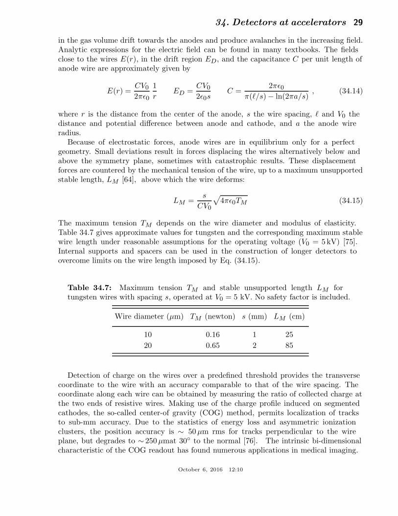
34. Detectors at accelerators 29
in the gas volume drift towards the anodes and produce avalanches in the increasing field.Analytic expressions for the electric field can be found in many textbooks. The fieldsclose to the wires E(r), in the drift region ED, and the capacitance C per unit length ofanode wire are approximately given by
E(r) =CV0
2πǫ0
1
rED =
CV0
2ǫ0sC =
2πǫ0π(ℓ/s)− ln(2πa/s)
, (34.14)
where r is the distance from the center of the anode, s the wire spacing, ℓ and V0 thedistance and potential difference between anode and cathode, and a the anode wireradius.
Because of electrostatic forces, anode wires are in equilibrium only for a perfectgeometry. Small deviations result in forces displacing the wires alternatively below andabove the symmetry plane, sometimes with catastrophic results. These displacementforces are countered by the mechanical tension of the wire, up to a maximum unsupportedstable length, LM [64], above which the wire deforms:
LM =s
CV0
√
4πǫ0TM (34.15)
The maximum tension TM depends on the wire diameter and modulus of elasticity.Table 34.7 gives approximate values for tungsten and the corresponding maximum stablewire length under reasonable assumptions for the operating voltage (V0 = 5kV) [75].Internal supports and spacers can be used in the construction of longer detectors toovercome limits on the wire length imposed by Eq. (34.15).
Table 34.7: Maximum tension TM and stable unsupported length LM fortungsten wires with spacing s, operated at V0 = 5 kV. No safety factor is included.
Wire diameter (µm) TM (newton) s (mm) LM (cm)
10 0.16 1 25
20 0.65 2 85
Detection of charge on the wires over a predefined threshold provides the transversecoordinate to the wire with an accuracy comparable to that of the wire spacing. Thecoordinate along each wire can be obtained by measuring the ratio of collected charge atthe two ends of resistive wires. Making use of the charge profile induced on segmentedcathodes, the so-called center-of gravity (COG) method, permits localization of tracksto sub-mm accuracy. Due to the statistics of energy loss and asymmetric ionizationclusters, the position accuracy is ∼ 50 µm rms for tracks perpendicular to the wireplane, but degrades to ∼ 250µmat 30 to the normal [76]. The intrinsic bi-dimensionalcharacteristic of the COG readout has found numerous applications in medical imaging.
October 6, 2016 12:10
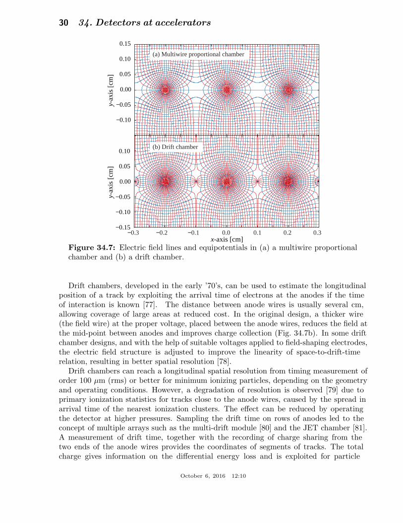
30 34. Detectors at accelerators
−0.15
−0.10
−0.05
0.00
0.05
0.10
x-axis [cm] −0.2−0.3 −0.1 0.0 0.1 0.2 0.3
−0.10
−0.05
0.00
0.05
0.10
0.15
y-ax
is [
cm]
y-ax
is [
cm]
(a) Multiwire proportional chamber
(b) Drift chamber
Figure 34.7: Electric field lines and equipotentials in (a) a multiwire proportionalchamber and (b) a drift chamber.
Drift chambers, developed in the early ’70’s, can be used to estimate the longitudinalposition of a track by exploiting the arrival time of electrons at the anodes if the timeof interaction is known [77]. The distance between anode wires is usually several cm,allowing coverage of large areas at reduced cost. In the original design, a thicker wire(the field wire) at the proper voltage, placed between the anode wires, reduces the field atthe mid-point between anodes and improves charge collection (Fig. 34.7b). In some driftchamber designs, and with the help of suitable voltages applied to field-shaping electrodes,the electric field structure is adjusted to improve the linearity of space-to-drift-timerelation, resulting in better spatial resolution [78].
Drift chambers can reach a longitudinal spatial resolution from timing measurement oforder 100 µm (rms) or better for minimum ionizing particles, depending on the geometryand operating conditions. However, a degradation of resolution is observed [79] due toprimary ionization statistics for tracks close to the anode wires, caused by the spread inarrival time of the nearest ionization clusters. The effect can be reduced by operatingthe detector at higher pressures. Sampling the drift time on rows of anodes led to theconcept of multiple arrays such as the multi-drift module [80] and the JET chamber [81].A measurement of drift time, together with the recording of charge sharing from thetwo ends of the anode wires provides the coordinates of segments of tracks. The totalcharge gives information on the differential energy loss and is exploited for particle
October 6, 2016 12:10
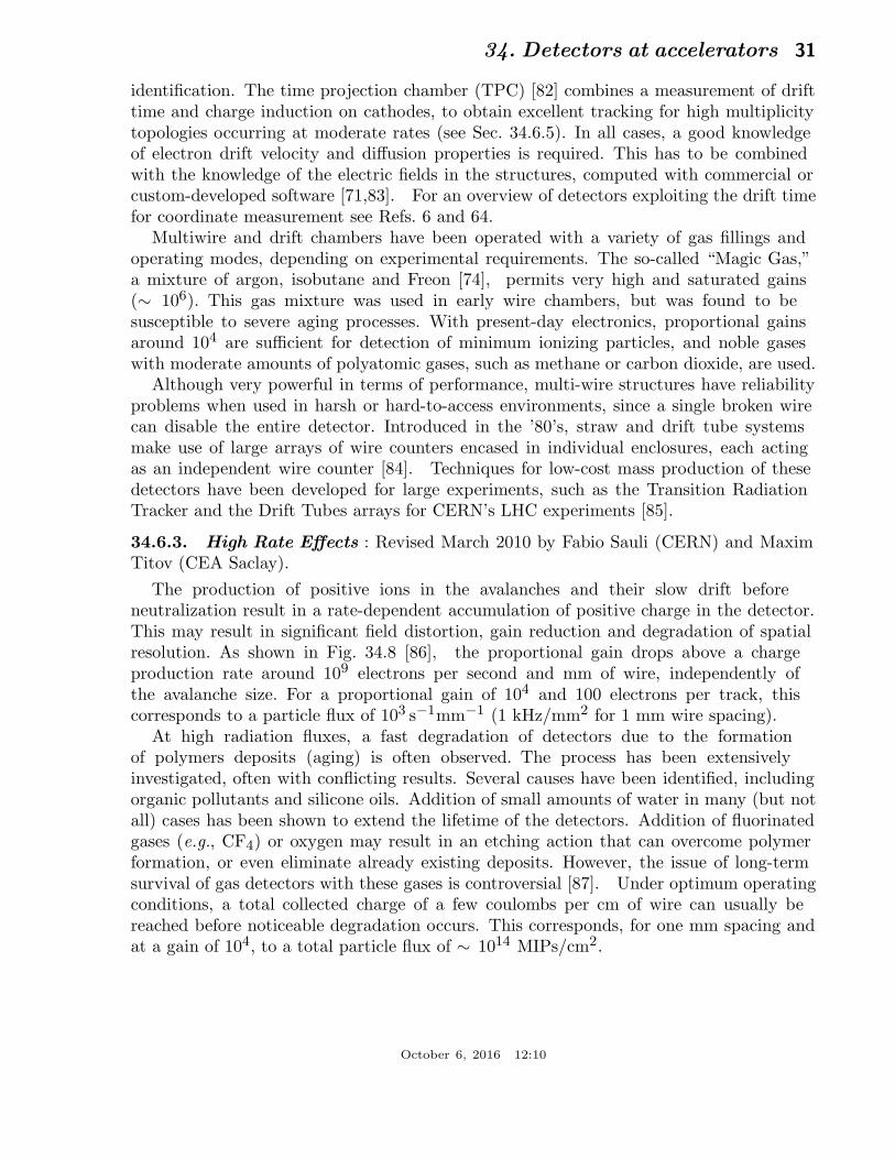
34. Detectors at accelerators 31
identification. The time projection chamber (TPC) [82] combines a measurement of drifttime and charge induction on cathodes, to obtain excellent tracking for high multiplicitytopologies occurring at moderate rates (see Sec. 34.6.5). In all cases, a good knowledgeof electron drift velocity and diffusion properties is required. This has to be combinedwith the knowledge of the electric fields in the structures, computed with commercial orcustom-developed software [71,83]. For an overview of detectors exploiting the drift timefor coordinate measurement see Refs. 6 and 64.
Multiwire and drift chambers have been operated with a variety of gas fillings andoperating modes, depending on experimental requirements. The so-called “Magic Gas,”a mixture of argon, isobutane and Freon [74], permits very high and saturated gains(∼ 106). This gas mixture was used in early wire chambers, but was found to besusceptible to severe aging processes. With present-day electronics, proportional gainsaround 104 are sufficient for detection of minimum ionizing particles, and noble gaseswith moderate amounts of polyatomic gases, such as methane or carbon dioxide, are used.
Although very powerful in terms of performance, multi-wire structures have reliabilityproblems when used in harsh or hard-to-access environments, since a single broken wirecan disable the entire detector. Introduced in the ’80’s, straw and drift tube systemsmake use of large arrays of wire counters encased in individual enclosures, each actingas an independent wire counter [84]. Techniques for low-cost mass production of thesedetectors have been developed for large experiments, such as the Transition RadiationTracker and the Drift Tubes arrays for CERN’s LHC experiments [85].
34.6.3. High Rate Effects : Revised March 2010 by Fabio Sauli (CERN) and MaximTitov (CEA Saclay).
The production of positive ions in the avalanches and their slow drift beforeneutralization result in a rate-dependent accumulation of positive charge in the detector.This may result in significant field distortion, gain reduction and degradation of spatialresolution. As shown in Fig. 34.8 [86], the proportional gain drops above a chargeproduction rate around 109 electrons per second and mm of wire, independently ofthe avalanche size. For a proportional gain of 104 and 100 electrons per track, thiscorresponds to a particle flux of 103 s−1mm−1 (1 kHz/mm2 for 1 mm wire spacing).
At high radiation fluxes, a fast degradation of detectors due to the formationof polymers deposits (aging) is often observed. The process has been extensivelyinvestigated, often with conflicting results. Several causes have been identified, includingorganic pollutants and silicone oils. Addition of small amounts of water in many (but notall) cases has been shown to extend the lifetime of the detectors. Addition of fluorinatedgases (e.g., CF4) or oxygen may result in an etching action that can overcome polymerformation, or even eliminate already existing deposits. However, the issue of long-termsurvival of gas detectors with these gases is controversial [87]. Under optimum operatingconditions, a total collected charge of a few coulombs per cm of wire can usually bereached before noticeable degradation occurs. This corresponds, for one mm spacing andat a gain of 104, to a total particle flux of ∼ 1014 MIPs/cm2.
October 6, 2016 12:10
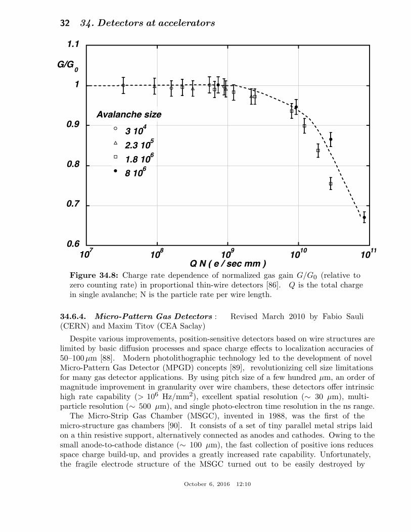
32 34. Detectors at accelerators
Figure 34.8: Charge rate dependence of normalized gas gain G/G0 (relative tozero counting rate) in proportional thin-wire detectors [86]. Q is the total chargein single avalanche; N is the particle rate per wire length.
34.6.4. Micro-Pattern Gas Detectors : Revised March 2010 by Fabio Sauli(CERN) and Maxim Titov (CEA Saclay)
Despite various improvements, position-sensitive detectors based on wire structures arelimited by basic diffusion processes and space charge effects to localization accuracies of50–100µm [88]. Modern photolithographic technology led to the development of novelMicro-Pattern Gas Detector (MPGD) concepts [89], revolutionizing cell size limitationsfor many gas detector applications. By using pitch size of a few hundred µm, an order ofmagnitude improvement in granularity over wire chambers, these detectors offer intrinsichigh rate capability (> 106 Hz/mm2), excellent spatial resolution (∼ 30 µm), multi-particle resolution (∼ 500 µm), and single photo-electron time resolution in the ns range.
The Micro-Strip Gas Chamber (MSGC), invented in 1988, was the first of themicro-structure gas chambers [90]. It consists of a set of tiny parallel metal strips laidon a thin resistive support, alternatively connected as anodes and cathodes. Owing to thesmall anode-to-cathode distance (∼ 100 µm), the fast collection of positive ions reducesspace charge build-up, and provides a greatly increased rate capability. Unfortunately,the fragile electrode structure of the MSGC turned out to be easily destroyed by
October 6, 2016 12:10
34. Detectors at accelerators 33
discharges induced by heavily ionizing particles [91]. Nevertheless, detailed studies oftheir properties, and in particular, on the radiation-induced processes leading to dischargebreakdown, led to the development of the more powerful devices: GEM and Micromegas.These have improved reliability and radiation hardness. The absence of space-chargeeffects in GEM detectors at the highest rates reached so far and the fine granularity ofMPGDs improve the maximum rate capability by more than two orders of magnitude(Fig. 34.9) [78,92]. Even larger rate capability has been reported for Micromegas [93].
Figure 34.9: Normalized gas gain as a function of particle rate for MWPC [78]and GEM [92].
The Gas Electron Multiplier (GEM) detector consists of a thin-foil copper-insulator-copper sandwich chemically perforated to obtain a high density of holes in whichavalanches occur [94]. The hole diameter is typically between 25 µm and 150 µm, whilethe corresponding distance between holes varies between 50 µm and 200 µm. The centralinsulator is usually (in the original design) the polymer Kapton, with a thickness of50 µm. Application of a potential difference between the two sides of the GEM generatesthe electric fields indicated in Fig. 34.10. Each hole acts as an independent proportionalcounter. Electrons released by the primary ionization particle in the upper conversionregion (above the GEM foil) drift into the holes, where charge multiplication occurs inthe high electric field (50–70 kV/cm). Most of avalanche electrons are transferred intothe gap below the GEM. Several GEM foils can be cascaded, allowing the multi-layerGEM detectors to operate at overall gas gain above 104 in the presence of highly ionizingparticles, while strongly reducing the risk of discharges. This is a major advantage of the
October 6, 2016 12:10

34 34. Detectors at accelerators
GEM technology [95]. Localization can then be performed by collecting the charge on apatterned one- or two-dimensional readout board of arbitrary pattern, placed below thelast GEM.
140 µm
50 µm
Figure 34.10: Schematic view and typical dimensions of the hole structure in theGEM amplification cell. Electric field lines (solid) and equipotentials (dashed) areshown.
The micro-mesh gaseous structure (Micromegas) is a thin parallel-plate avalanchecounter, as shown in Fig. 34.11 [96]. It consists of a drift region and a narrowmultiplication gap (25–150 µm) between a thin metal grid (micromesh) and the readoutelectrode (strips or pads of conductor printed on an insulator board). Electrons from theprimary ionization drift through the holes of the mesh into the narrow multiplication gap,where they are amplified. The electric field is homogeneous both in the drift (electricfield ∼ 1 kV/cm) and amplification (50–70 kV/cm) gaps. In the narrow multiplicationregion, gain variations due to small variations of the amplification gap are approximatelycompensated by an inverse variation of the amplification coefficient, resulting in a moreuniform gain. The small amplification gap produces a narrow avalanche, giving rise toexcellent spatial resolution: 12 µm accuracy, limited by the micro-mesh pitch, has beenachieved for MIPs, as well as very good time resolution and energy resolution (∼ 12%FWHM with 6 keV x rays) [97].
The performance and robustness of GEM and Micromegas have encouraged their usein high-energy and nuclear physics, UV and visible photon detection, astroparticle and
October 6, 2016 12:10

34. Detectors at accelerators 35
HV1
HV2Micromesh
100
µm
Anode plane
e−
E2
50-70 kV/cm
Particle
Drift gap
Amplificationgap
Figure 34.11: Schematic drawing of the Micromegas detector.
neutrino physics, neutron detection and medical physics. Most structures were originallyoptimized for high-rate particle tracking in nuclear and high-energy physics experiments.COMPASS, a high-luminosity experiment at CERN, pioneered the use of large-area(∼ 40 × 40 cm2) GEM and Micromegas detectors close to the beam line with particlerates of 25 kHz/mm2. Both technologies achieved a tracking efficiency of close to 100%at gas gains of about 104, a spatial resolution of 70–100 µm and a time resolutionof ∼ 10 ns. GEM detectors are also used for triggering in the LHCb Muon Systemand for tracking in the TOTEM Telescopes. Both GEM and Micromegas devices areforeseen for the upgrade of the LHC experiments and for one of the readout optionsfor the Time Projection Chamber (TPC) at the International Linear Collider (ILC).The development of new fabrication techniques—“bulk” Micromegas technology [98] andsingle-mask GEMs [99] —is a big step toward industrial production of large-size MPGDs.In some applications requiring very large-area coverage with moderate spatial resolution,coarse macro-patterned detectors, such as Thick GEMs (THGEM) [100] or patternedresistive-plate devices [101] might offer economically interesting solutions.
Sensitive and low-noise electronics enlarge the range of the MPGD applications.Recently, the GEM and Micromegas detectors were read out by high-granularity (∼ 50 µmpitch) CMOS chips assembled directly below the GEM or Micromegas amplificationstructures [102]. These detectors use the bump-bonding pads of a pixel chip as anintegrated charge collecting anode. With this arrangement signals are induced at theinput gate of a charge-sensitive preamplifier (top metal layer of the CMOS chip). Everypixel is then directly connected to the amplification and digitization circuits, integratedin the underlying active layers of the CMOS technology, yielding timing and chargemeasurements as well as precise spatial information in 3D.
The operation of a MPGD with a Timepix CMOS chip has demonstrated the possibility
October 6, 2016 12:10

36 34. Detectors at accelerators
of reconstructing 3D-space points of individual primary electron clusters with ∼ 30 µmspatial resolution and event-time resolution with nanosecond precision. This has becomeindispensable for tracking and triggering and also for discriminating between ionizingtracks and photon conversions. The GEM, in conjunction with a CMOS ASIC,* candirectly view the absorption process of a few keV x-ray quanta and simultaneouslyreconstruct the direction of emission, which is sensitive to the x-ray polarization. Thanksto these developments, a micro-pattern device with finely segmented CMOS readout canserve as a high-precision “electronic bubble chamber.” This may open new opportunitiesfor x-ray polarimeters, detection of weakly interacting massive particles (WIMPs) andaxions, Compton telescopes, and 3D imaging of nuclear recoils.
An elegant solution for the construction of the Micromegas with pixel readout is theintegration of the amplification grid and CMOS chip by means of an advanced “waferpost-processing” technology [103]. This novel concept is called “Ingrid” (see Fig. 34.12).With this technique, the structure of a thin (1µm) aluminum grid is fabricated on top ofan array of insulating pillars. which stands ∼ 50µm above the CMOS chip. The sub-µmprecision of the grid dimensions and avalanche gap size results in a uniform gas gain.The grid hole size, pitch and pattern can be easily adapted to match the geometry of anypixel readout chip.
Figure 34.12: Photo of the Micromegas “Ingrid” detector. The grid holes can beaccurately aligned with readout pixels of CMOS chip. The insulating pillars arecentered between the grid holes, thus avoiding dead regions.
Recent developments in radiation hardness research with state-of-the-art MPGDs arereviewed in Ref. 104. Earlier aging studies of GEM and Micromegas concepts revealed
* Application Specific Integrated Circuit
October 6, 2016 12:10
34. Detectors at accelerators 37
that they might be even less vulnerable to radiation-induced performance degradationthan standard silicon microstrip detectors.
The RD51 collaboration was established in 2008 to further advance technologicaldevelopments of micro-pattern detectors and associated electronic-readout systems forapplications in basic and applied research [105].
34.6.5. Time-projection chambers : Written August 2015 by C. Lippmann (GSIHelmholtzzentrum fur Schwerionenforschung, Darmstadt, Germany)
The Time Projection Chamber (TPC) concept was invented by David Nygren in thelate 1970’s [82]. It consists of a cylindrical or square field cage filled with a detectionmedium that is usually a gas or a liquid. Charged particles produce tracks of ionizationelectrons that drift in a uniform electric field towards a position-sensitive amplificationstage which provides a 2D projection of the particle trajectories. The third coordinatecan be calculated from the arrival times of the drifted electrons. The start for this drifttime measurement is usually derived from an external detector, e.g. a fast interactiontrigger detector.
This section focuses on the gas-filled TPCs that are typically used in particle or nuclearphysics experiments at accelerators due to their low material budget. For neutrino physics(Sec. 34.10) or for detecting rare events (Sec. 35.4), on the contrary, usually high densityand large active mass are required, and a liquid detection medium is favored.
The TPC enables full 3D measurements of charged particle tracks, which gives it adistinct advantage over other tracking detector designs which record information onlyin two-dimensional detector planes and have less overall segmentation. This advantageis often exploited for pattern recognition in events with large numbers of particles,e.g. heavy-ion collisions. Two examples of modern large-volume gaseous TPCs are shownin Fig. 34.13 and Fig. 34.14.
Identification of the charged particles crossing the TPC is possible by simultaneouslymeasuring their momentum and specific energy deposit through ionisation (dE/dx). Themomentum, as well as the charge sign, are calculated from a helix fit to the particletrajectory in the presence of a magnetic field (typically parallel to the drift field). Forthis application, precise spatial measurements in the plane transverse to the magneticfield are most important. The specific energy deposit is estimated from many chargemeasurements along the particle trajectory (e.g. one measurement per anode wire orper row of readout pads). As the charge collected per readout segment depends on thetrack angle and on the ambient conditions, the measured values are corrected for theeffective length of the track segments and for variations of the gas temperature andpressure. The most probable value of the corrected signal amplitudes provides the bestestimator for the specific energy deposit (see Sec. 33.2.3); it is usually approximatedby the truncated mean, i.e. the average of the 50%-70% smallest values. The resultingparticle identification performance is illustrated in Fig. 34.15, for the ALICE TPC.
The dependence of the achievable energy resolution on the number of measurementsN , on the thickness of the sampling layers t, and on the gas pressure P can be estimatedusing an empirical formula [109]:
σdE/dx = 0.41 N−0.43(t P )−0.32. (34.16)
October 6, 2016 12:10
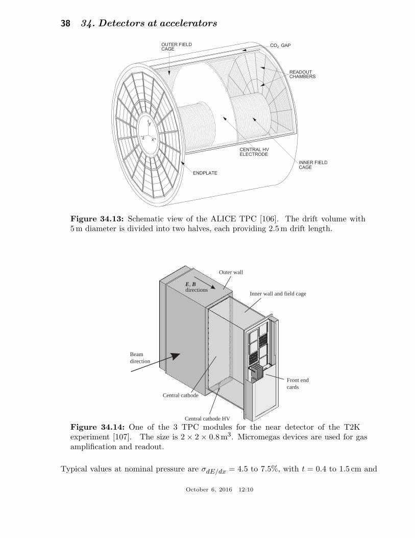
38 34. Detectors at accelerators
Figure 34.13: Schematic view of the ALICE TPC [106]. The drift volume with5m diameter is divided into two halves, each providing 2.5m drift length.
Inner wall and field cage
Outer wall
E, Bdirections
Front endcards
Beamdirection
Central cathode
Central cathode HV
Figure 34.14: One of the 3 TPC modules for the near detector of the T2Kexperiment [107]. The size is 2 × 2 × 0.8m3. Micromegas devices are used for gasamplification and readout.
Typical values at nominal pressure are σdE/dx = 4.5 to 7.5%, with t = 0.4 to 1.5 cm and
October 6, 2016 12:10

34. Detectors at accelerators 39
Momentum (GeV/c)
1−10 1 10
π
μ
e
K p d t ALICE performance
= 13 TeVspp,
B = 0.2 T
En
erg
y d
ep
osit p
er
un
it le
ng
th (
ke
V/c
m)
10
8
6
5
4
3
2
20
30
Figure 34.15: Energy deposit versus momentum measured in the ALICETPC [108].
N = 40 up to more than 300. Due to the high gas pressure of 8.5 bar, the resolutionachieved with the PEP-4/9 TPC was an unprecedented 3% [110].
The greatest challenges for a large TPC are due to the length of the drift of up toseveral meters. In particular, it can make the device sensitive to small distortions in theelectric field. Such distortions can arise from a number of sources, e.g. imperfectionsin the field cage construction or the presence of ions in the drift volume. The electrondrift in a TPC in the presence of a magnetic field is defined by Eq. (34.13). The E ×Bterm of Eq. (34.13) vanishes for perfectly aligned electric and magnetic fields, which canhowever be difficult to achieve in practice. Furthermore, the electron drift depends on theωτ factor, which is defined by the chosen gas mixture and magnetic field strength. Theelectrons will tend to follow the magnetic field lines for ωτ > 1 or the electric field lines forωτ < 1. The former mode of operation makes the TPC less sensitive to non-uniformitiesof the electric field, which is usually desirable.
The drift of the ionization electrons is superposed with a random diffusion motionwhich degrades their position information. The ultimate resolution of a single positionmeasurement is limited to around
σx =σD
√L√
n, (34.17)
where σD is the transverse diffusion coefficient for 1 cm drift, L is the drift length in cmand n is the effective number of electrons collected. Without a magnetic field, σD,B=0
√L
is typically a few mm after a drift of L = 100 cm. However, in a strong magnetic field
October 6, 2016 12:10
40 34. Detectors at accelerators
parallel to the drift field, a large value of ωτ can significantly reduce diffusion:
σD,B>0
σD,B=0=
1√1 + ω2τ2
. (34.18)
This factor can reach values of up to 10. In practice, the final resolution limit due todiffusion will typically be around σx = 100 µm.
The drift and diffusion of electrons depend strongly on the nature of the gas that isused. The optimal gas mixture varies according to the environment in which the TPCwill operate. In all cases, the oxygen concentration must be kept very low (few ten partsper million in a large TPC) in order to avoid electron loss through attachment. Ideally,the drift velocity should depend only weakly on the electric field at the nominal operatingcondition. The classic Ar/CH4 (90:10) mixture, known as P10, has a drift velocitymaximum of 5 cm/µs at an electric field of only 125V/cm (Fig. 34.4). In this regime,the electron arrival time is not affected by small variations in the ambient conditions.Moreover, low electric fields simplify the design and operation of the field cage. Themixture has a large transverse diffusion at B = 0, but this can be reduced significantly ina strong magnetic field due to the relatively large value of ωτ .
For certain applications, organic gases like CH4 are not desirable, since they may causeaging. An alternative is to replace CH4 with CO2. An Ar/CO2 (90:10) mixture featuresa low transverse diffusion at all magnetic field strengths, but does not provide a saturateddrift velocity for the typical electric fields used in TPCs (up to a few 100V/cm), so it isquite sensitive to the ambient conditions. Freon admixtures like CF4 can be an attractiveoption for a TPC as well, since the resulting gas mixtures provide high drift velocities atlow electric fields. However, the use of CF4 always needs to be thoroughly validated forcompatibility with all materials of the detector and the gas system.
Historically, the amplification stages used in gaseous TPCs have been planes of anodewires operated in proportional mode. The performance is limited by effects related to thefeature size of a few mm (wire spacing). Since near the wires the electric and magneticfields are not parallel, the incoming ionisation electrons are displaced in the directionof the wires (“wire E × B effect”), which degrades the resolution. The smaller featuresizes of Micro-Pattern Gas Detectors (MPGDs) like GEMs and Micromegas lead to manyadvantages as compared to wire planes (see Sec. 34.6.4). In particular, E × B effectsin the amplification stage are much smaller. Moreover, the signal induction process inMPGDs leads to a very narrow pad response, allowing for a much finer segmentationand improving the separation of two nearby tracks. Combinations of MPGDs with siliconsensors have resulted in the highest granularity readout systems so far (see Sec. 34.6.4).These devices make it possible to count the number of ionization clusters along the lengthof a track, which can, in principle, improve the particle identification capability. However,the big challenge for such a system is the huge number of read-out channels for a TPC ofa typical size.
The accumulation of the positive ions created by the ionization from the particle trackscan lead to time-dependent distortions of the drift field. Due to their small drift velocity,ions from many events may coexist in the drift volume. To reduce the effect of such abuild-up of space charge, Argon can be replaced by Neon as the main component of the
October 6, 2016 12:10

34. Detectors at accelerators 41
gas mixture. Neon features a lower number of ionisation electrons per unit of track length(see Table 34.5) and a higher ion mobility (see Table 34.6).
Of much greater concern are the ions produced in the gas amplification stage. In orderto prevent them from entering the drift volume, large TPCs built until now usually have agating grid. The gating grid can be switched to transparent mode (usually in the presenceof an interaction trigger) to allow the ionization electrons to pass into the amplificationregion. After all electrons have reached the amplification region, it is usually closed suchthat it is rendered opaque to electrons and ions.
Alternatively, new readout schemes are being developed using MPGDs. These can beoptimized in a way that they release many fewer positive ions than wire planes operatingat the same effective gain. This is an exciting possibility for future TPCs.
34.6.6. Transition radiation detectors (TRD’s) : Revised August 2013 byP. Nevski (BNL) and A. Romaniouk (Moscow Eng. & Phys. Inst.)
Transition radiation (TR) x-rays are produced when a highly relativistic particle(γ >∼ 103) crosses a refractive index interface, as discussed in Sec. 33.7. The x-rays,ranging from a few keV to a few dozen keV or more, are emitted at a characteristic angle1/γ from the particle trajectory. Since the TR yield is about 1% per boundary crossing,radiation from multiple surface crossings is used in practical detectors. In the simplestconcept, a detector module might consist of low-Z foils followed by a high-Z active layermade of proportional counters filled with a Xe-rich gas mixture. The atomic numberconsiderations follow from the dominant photoelectric absorption cross section per atomgoing roughly as Z n/E3
x, where n varies between 4 and 5 over the region of interest, andthe x-ray energy is Ex.* To minimize self-absorption, materials such as polypropylene,Mylar, carbon, and (rarely) lithium are used as radiators. The TR signal in the activeregions is in most cases superimposed upon the particle ionization losses, which areproportional to Z.
The TR intensity for a single boundary crossing always increases with γ, but, formultiple boundary crossings, interference leads to saturation above a Lorentz factor γ sat
= 0.6 ω1√
ℓ1ℓ2/c [111], where ω1 is the radiator material plasma frequency, ℓ1 is itsthickness, and ℓ2 the spacing. In most of the detectors used in particle physics theradiator parameters are chosen to provide γ sat ≈ 2000. Those detectors normally workas threshold devices, ensuring the best electron/pion separation in the momentum range1 GeV/c <∼ p <∼ 150 GeV/c.
One can distinguish two design concepts—“thick” and “thin” detectors:1. The radiator, optimized for a minimum total radiation length at maximum TR yield
and total TR absorption, consists of few hundred foils (for instance 300 20 µm thickpolypropylene foils). Most of the TR photons are absorbed in the radiator itself. Tomaximise the number of TR photons reaching the detector, part of the radiator farfrom the active layers is often made of thicker foils, which shifts the x-ray spectrumto higher energies. The detector thickness, about 2-4 cm for Xe-filled gas chambers, isoptimized to absorb the incoming x-ray spectrum. A classical detector is composed of
* Photon absorption coefficients for the elements (via a NIST link), and dE/dx|min andplasma energies for many materials are given in pdg.lbl.gov/AtomicNuclearProperties.
October 6, 2016 12:10

42 34. Detectors at accelerators
several similar modules which respond nearly independently. Such detectors were usedin the UA2, NA34 and other experiments [112], and are being used in the ALICEexperiment [113], [114].
2. In other TRD concepts a fine granular radiator/detector structure exploits the soft partof the TR spectrum more efficiently and thereby may act also as an integral part of thetracking detector. This can be achieved, for instance, by distributing small-diameterstraw-tube detectors uniformly or in thin layers throughout the radiator material(foils or fibers). Even with a relatively thin radiator stack, radiation below 5 keV ismostly lost in the radiators themselves. However for photon energies above this value,the absorption is reduced and the radiation can be registered by several consecutivedetector layers, thus creating a strong TR build-up effect. This approach allows torealise TRD as an integral part of the tracking detector. Descriptions of detectorsusing this approach can be found in both accelerator and space experiments [113,114].For example, in the ATLAS TR tracker (TRT), charged particles cross about 35effective straw tube layers embedded in the radiator material [113]. The effectivethickness of the Xe gas per straw is about 2.2 mm and the average number of foils perstraw is about 40 with an effective foil thickness of about 18 µm.Both TR photon absorption and the TR build-up significantly affect the detector
performance. Although the values mentioned above are typical for most of the plasticradiators used with Xe-based detectors, they vary significantly depending on the detectorparameters: radiator material, thickness and spacing, the geometry and position of thesensitive chambers, etc. Thus careful simulations are usually needed to build a detectoroptimized for a particular application. For TRD simulation stand-alone codes based onGEANT3 program were usually used (P.Nevski in [113]) . TR simulation is now availablein GEANT4 [118]. The most recent version of it (starting from release 9.5) shows areasonable agreement with data (S. Furletov in [114] and [115]) .
The discrimination between electrons and pions can be based on the charge depositionmeasured in each detection module, on the number of clusters – energy depositionsobserved above an optimal threshold (usually it is 5–7 keV ), or on more sophisticatedmethods such as analyzing the pulse shape as a function of time. The total energymeasurement technique is more suitable for thick gas volumes, which absorb most of theTR radiation and where the ionization loss fluctuations are small. The cluster-countingmethod works better for detectors with thin gas layers, where the fluctuations of theionization losses are big. Cluster-counting replaces the Landau-Vavilov distribution ofbackground ionization energy losses with the Poisson statistics of δ-electrons, responsiblefor the distribution tails. The latter distribution is narrower than the Landau-Vavilovdistribution. In practice, most of the experiments use a likelihood method, which exploitsdetailed knowledge of the detector response for different particles and gives the bestseparation. The more parameters that are considered, the better separation power.The recent results of the TRD in the AMS experiment is a good example. In the realexperiment the rejection power is better by almost one order of magnitude than thatobtained in the beam test if stringent criteria for track selection are applied (see T. Kirnet al. in [114]) . Another example is a neural network method used by the ALICE TRD(ALICE point in Fig. 34.16) which gives another factor of 2–3 in rejecton power with
October 6, 2016 12:10

34. Detectors at accelerators 43
0.01
0.1
0.001
10 20 50 200100
NA34 (HELIOS)C.Fabjan et al.R 806A. Bungener et al.ZEUS
KEKUA2H.Butt et al.D0M.Holder et al.H.WeidkampH.Grassler et al.
ATLAS
NOMAD
AMS
Total detector length (cm)
Pion
eff
icie
ncy
ALICEPAMELA
..
..
Figure 34.16: Pion efficiency measured (or predicted) for different TRDs as afunction of the detector length for a fixed electron efficiency of 90%. The plotis taken from [112]. Results from more recent detectors are added from [113]and [114].
respect to the likelihood method [116]) .The major factor in the performance of any TRD is its overall length. This is
illustrated in Fig. 34.16, which shows, for a variety of detectors, the pion efficiencyat a fixed electron efficiency of 90% as a function of the overall detector length. TRDperformance depends on particle energy and in this figure the experimental data, coveringa range of particle energies from 1 GeV to 40 GeV, are rescaled to an energy of 10GeV when possible. Phenomenologically, the rejection power against pions increases as5 · 10L/38, where the range of validity is L ≈ 20–100 cm. Apart from the beam energyvariations, the observed scattering of the points in the plot reflects how effectively thedetector space is used and how well the exact response to different particles is takeninto account in the analysis. For instance, the ATLAS TRT was built as a compromisebetween TR and tracking requirements; that is why the test-beam prototype result (lowerpoint) is better than the real TRT performance at the LHC shown in Fig. 34.16 fordifferent regions in the detector (in agreement with MC).
In most cases, recent TRDs combine particle identification with charged-trackmeasurement in the same detector [113,114,117]. This is particularly important forcollider experiments, where the available space for the inner detector is very limited. Fora modest increase of the radiation length due to the radiator (∼4% X0), a significantenhancement of the electron identification was obtained in the case of the ATLAS TRT.
October 6, 2016 12:10
44 34. Detectors at accelerators
The combination of the two detector functions provides a powerful tool for electronidentification even at very high particle densities.
In addition to the enhancement of the electron identification, one of the most importantroles of the TRDs in the collider experiments is their participation in different trigger anddata analysis algorithms. The ALICE experiment [114] is a good example of the use of theTRD in a First Level Trigger. In the ATLAS experiment, the TRT information is usedin the High Level Trigger (HLT) algorithms. With continuous increase of instantaneousluminosity, the electron trigger output rate becomes so high, that a significant increaseof the calorimeter energy threshold is required to keep it at an acceptable level. Forluminosities above 2 · 1034cm−2s−1 at the LHC this will affect the trigger efficiency ofvery important physics channels (e.g. W → eν inclusive decay). Even a very soft TR cutat HLT level, which preserves high electron efficiency (98%), allows to maintain a hightrigger efficiency and its purity for physics events with a single electron in a final state.TRT also plays a crucial role in the studies where an electron suppression is required(e.g. hadronic mode of τ–decays). TR information is a completely independent tool forelectron identification and allows to study systematic uncertainties of other electronreconstruction methods.
Electron identification is not the only TRD application. Recent TRDs for particleastrophysics are designed to directly measure the Lorentz factor of high-energy nuclei byusing the quadratic dependence of the TR yield on nuclear charge; see Cherry and Mullerpapers in [113]. The radiator configuration (ℓ1, ℓ2) is tuned to extend the TR yield riseup to γ <∼ 105 using the more energetic part of the TR spectrum (up to 100 keV). Largedensity radiator materials (such as Al) are the best for this purpose. Direct absorptionof the TR-photons of these energies with thin detectors becomes problematic and TRdetection methods based on Compton scattering have been proposed to use (M. Cherryin [113], [114]) .
In all cases to-date, the radiator properties have been the main limiting factor for theTRDs, and for future progress in this field, it is highly important to develop effectiveand compact radiators. By now, all traditional materials have been studied extensively,so new technologies must be invented. The properties of all radiators are defined by onebasic parameter which is the plasma frequency of the radiator material – ω1 ∼ 1/me
(see Eq. (33.48)). In semiconductor materials, a quantum mechanical treatment of theelectron binding to the lattice leads to a small effective electron mass and correspondinglyto large values of ω1. All semiconductor materials have large Z and may not be goodcandidates as TR radiators, but new materials, such as graphene, may offer similarfeatures at much lower Z (M. Cherry in [114]) . It might even be possible to producegraphene-based radiators with the required ω1 value. One should take into account thatTR cutoff energy – Ec ∼ ω1γ and 95% of TR energy belongs to an interval of 0.1Ec
to Ec. For large ω1 the detector must have a larger thickness to absorb x-rays in thisrange. It would be important to control ω1 during radiator production and use it as afree parameter in the detector optimization process.
Si-microstrip tracking detectors operating in a magnetic field can also be used forTR detection, even though the dE/dx losses in Si are much larger than the absorbedTR energy. The excellent spatial resolution of the Si detectors provides separation of
October 6, 2016 12:10

34. Detectors at accelerators 45
the TR photons and dE/dx losses at relatively modest distances between radiator anddetector. Simulations made on the basis of the beam-test data results has shown that ina magnetic field of 2 T and for the geometry of the ATLAS Si-tracker proposed for sLHC,a rejection factor of > 30 can be obtained for an electron efficiency above 90% over aparticle momentum range 2-30 GeV/c (Brigida et al. in [113] and [114]) . New detectortechniques for TRDs are also under development and among them one should mentionGasPixel detectors which allow to obtain a space point accuracy of < 30 µm and exploitall details of the particle tracks to highlight individual TR clusters in the gas (F. Harjeset al. in [114]) . Thin films of heavy scintillators (V.V Berdnikovet al. in [114]) might bevery attractive in a combination with new radiators mentioned above.
34.6.7. Resistive-plate chambers : Written July 2015 by G. Aielli (U. Roma TorVergata).
The resistive-plate chamber (RPC) is a gaseous detector developed by R. Santonicoand R. Cardarelli in the early 1980’s [119] *. Although its first purpose was to providea competitive alternative to large scintillator counters, it was quickly recognized thatit had relevant potential as a timing tracker due to the high space-time localizationof the discharge. The RPC, as sketched in Fig. 34.17, is a large planar capacitor withtwo parallel high bulk resistivity electrode plates (109–1013 Ω·cm) separated by a setof insulating spacers. The spacers define a gap in the range from a few millimetersdown to 0.1 mm with a precision of a few ∼ µm. The gap is filled with a suitableatmospheric-pressure gas mixture which serves as a target for ionizing radiation. Primaryionization for sub-millimeter gas gaps can be insufficient, thus multiple gaps can becombined to ensure an acceptable detection efficiency [121].
Induced negative
signal on Y strip
Induced positive
signal on X strip
Insulating foil
HV contact
Graphite layer
Low density filler 3 mm
Copper ground plane
Resistive electrode 2 mm
Gas 2 mmspacerFrameHV
Figure 34.17: Schematic cross section of a generic single gap RPC.
The electrodes are most commonly made of high pressure phenolic-melaminic laminate(HPL), improperly referred to as ”bakelite”, or glass. A moderate electrode resistivity(∼ 105 Ω/¤) establishes a uniform electric field of several kV/mm across the gap,which initiates an electron avalanche following primary ionization. The above resistivityis low enough to ensure uniformity of the electric field, yet still transparent to fast
* The RPC was based on earlier work on a spark counter with one metallic and onehigh-resistivity plate [120].
October 6, 2016 12:10

46 34. Detectors at accelerators
signal transients from avalanches. This field configuration allows an excellent space-timelocalization of the signal. Due to the high electrode resistivity in RPCs, the electrodetime constant is much longer than discharge processes. Therefore only the locally-storedelectrostatic energy contributes to the discharge, which prevents the formation of sparksand leaves the rest of the detector field unaffected. The gas-facing surface of HPLelectrodes are commonly coated with a resistive varnish (e.g. ∼ µm layer of polymerizedlinseed oil) to achieve the necessary resistivity as well as to protect the electrode fromdischarge damage. As with other gaseous detectors, the gas mixture is optimized foreach specific application. In general it needs to contain a component to quench UVphotons, thus avoiding discharge propagation. An electronegative component controlsthe avalanche growth in case of very high electric fields [122,123]. To first order, eachprimary ionization in an RPC is exponentially amplified according to its distance fromthe anode. Therefore RPC signals span a large dynamic range, unlike gaseous detectorswhere ionization and amplification occur in separate regions (e.g. wire chambers orMPGDs). For increasingly stronger fields, the avalanche exponential growth progressivelysaturates to linear [124], and finally reaches a strongly-saturated ”streamer” transitionwhich exhausts all the locally-available energy [125]. The signal induced by the fastmovement of the avalanche electrons is isotropically distributed with respect to the fielddirection and present with equal but opposite amplitude on the two electrodes. A setof metallic readout electrodes (e.g. pads or strips) placed behind the resistive electrodesdetect the charge pulse. This feature allows for 2D localization of the signal with uniformspatial resolution. Sensitivity to high-frequency electron avalanche signals over large RPCareas requires a correspondingly adequate Faraday cage and readout structure design. Inparticular, the front end electronics must be time-sensitive with a fast response and lownoise, although these requirements are usually in competition [126].
34.6.7.1. RPC types and applications: RPCs are generally classified in two categoriesdepending on the gas gap structure: single gap RPCs (described above) and multiple gapRPCs (typically referred as mRPCs or timing RPCs). While they are both based on thesame principle they have different construction techniques, performance and limitations,making them suitable for different applications. Due to its simplicity and robustness,the single gap RPC is ideal for covering very large surfaces. Typical detector systemscan have sensitive surface areas up to ∼104 m2, with single module areas of a few m2,and a space-time resolution down to ∼0.4 ns × 100 µm [127,128]. Typical applicationsare in muon systems (e.g. the muon trigger systems of the LHC experiments) or groundand underground based cosmic rays and neutrino arrays [129]. Moreover, single gapRPCs have recently found an application in tracking calorimetry [130]. The mRPCallows for smaller gas gap thicknesses while still maintaining a sufficient gaseous target.Th most common version [131] consists of a stack of floating glass electrodes separatedby monofilament (i.e. fishing) line, sandwiched between two external electrodes whichprovide the high-voltage bias. The floating glass electrodes assume a potential determinedby the avalanche processes occurring between them. mRPCs have been largely used inTOF systems and in applications such as timing PET.
October 6, 2016 12:10

34. Detectors at accelerators 47
34.6.7.2. Time and space resolution: The RPC field configuration generates anavalanche which is strongly correlated in space and time to the original ionizing event.Space-time uncertainties generally arise from the statistical fluctuations of the ionizationand multiplication processes, and from the characteristics of the readout and front-endelectronics. The intrinsic signal latency is commonly in the ns range, making the RPCsuitable for applications where a low latency is essential. A higher time resolutionand shorter signal duration is correlated with a thinner gas gap, although a higherelectric field is required for sufficient avalanche development [131,132]. Typical timingperformances are from around 1 ns with a 2 mm gas gap, down to 20 ps for a stack ofseveral 0.1 mm gaps [133]. The mechanical delicacy of sub-mm gap structures currentlylimit this technique to small detector areas. Digital strip readouts are commonly used,with spatial resolution determined by the strip pitch and the cluster size (∼0.5 cm).Recent developments toward higher spatial resolutions are mostly based on chargecentroid techniques, benefiting from the availability of low-cost high-performance readoutelectronics. The present state of the art detectors have a combined space-time resolutionof ∼50 ps × 40 µm [134].
34.6.7.3. Rate capability and ageing: RPC rate capability is limited by the voltage dropon resistive electrodes, ∆V = Va − Vgas = I · R [135]. Here Va is the applied voltage,Vgas is the effective voltage on the gas, R = ρ · d/S is the total electrode resistanceand I is the working current. Expressing I as the particle flux Φ times an averagecharge per avalanche 〈Q〉 gives ∆V/Φ = ρ · d · 〈Q〉. A large I not only limits the ratecapability but also affects the long term performance of the detector. Discharges depletethe conductive properties of HPL electrodes [136]. In the presence of fluorocarbonsand water, discharges generate hydrofluoric acid (HF) which damages internal detectorsurfaces, particularly glass electrodes [137]. HF damage can be mitigated by preventingwater vapor contamination and by sufficient flushing of the gas gap. Operating in thestreamer regime puts low requirements on the front end electronics sensitivity, butgenerally limits the counting rate capability to ∼100 Hz/cm2 and requires stability over alarge gain range. Higher rate operation can be achieved by reducing gas gain in favor ofelectronic amplification. Increasing electronegative gases, such as C2H2F4 and SF6 [123],shifts the streamer transition to higher gains. With these techniques, stable performanceat high rates (e.g. 10 kHz/cm2) has been achieved for large area single gap RPCs [126].Additional techniques rely on the natural redundancy and small gain of multiple gapstructures [138] and electrodes made with lower resistivity materials [139].
34.7. Semiconductor detectors
Updated November 2013 by H. Spieler.
Semiconductor detectors provide a unique combination of energy and positionresolution. In collider detectors they are most widely used as position sensing devices andphotodetectors (Sec. 34.2). Integrated circuit technology allows the formation of high-density micron-scale electrodes on large (15–20 cm diameter) wafers, providing excellentposition resolution. Furthermore, the density of silicon and its small ionization energyyield adequate signals with active layers only 100–300 µm thick, so the signals are alsofast (typically tens of ns). The high energy resolution is a key parameter in x-ray, gamma,
October 6, 2016 12:10

48 34. Detectors at accelerators
and charged particle spectroscopy, e.g., in neutrinoless double beta decay searches.Silicon and germanium are the most commonly used materials, but gallium-arsenide,CdTe, CdZnTe, and other materials are also useful. CdZnTe provides a higher stoppingpower and the ratio of Cd to Zn concentrations changes the bandgap. Ge detectors arecommonly operated at liquid nitrogen temperature to reduce the bias current, whichdepends exponentially on temperature. Semiconductor detectors depend crucially onlow-noise electronics (see Sec. 34.8), so the detection sensitivity is determined by signalcharge and capacitance. For a comprehensive discussion of semiconductor detectors andelectronics see Ref. 140 or the tutorial website http://www-physics.lbl.gov/ spieler.
34.7.1. Materials Requirements :Semiconductor detectors are essentially solid state ionization chambers. Absorbed
energy forms electron-hole pairs, i.e., negative and positive charge carriers, which underan applied electric field move towards their respective collection electrodes, where theyinduce a signal current. The energy required to form an electron-hole pair is proportionalto the bandgap. In tracking detectors the energy loss in the detector should be minimal,whereas for energy spectroscopy the stopping power should be maximized, so for gammarays high-Z materials are desirable.
Measurements on silicon photodiodes [141] show that for photon energies below 4 eVone electron-hole (e-h) pair is formed per incident photon. The mean energy Ei requiredto produce an e-h pair peaks at 4.4 eV for a photon energy around 6 eV. Above∼1.5 keV it assumes a constant value, 3.67 eV at room temperature. It is larger than thebandgap energy because momentum conservation requires excitation of lattice vibrations(phonons). For minimum-ionizing particles, the most probable charge deposition in a300 µm thick silicon detector is about 3.5 fC (22000 electrons). Other typical ionizationenergies are 2.96 eV in Ge, 4.2 eV in GaAs, and 4.43 eV in CdTe.
Since both electronic and lattice excitations are involved, the variance in the numberof charge carriers N = E/Ei produced by an absorbed energy E is reduced by theFano factor F (about 0.1 in Si and Ge). Thus, σN =
√FN and the energy resolution
σE/E =√
FEi/E. However, the measured signal fluctuations are usually dominatedby electronic noise or energy loss fluctuations in the detector. The electronic noisecontributions depend on the pulse shaping in the signal processing electronics, so thechoice of the shaping time is critical (see Sec. 34.8).
A smaller bandgap would produce a larger signal and improve energy resolution,but the intrinsic resistance of the material is critical. Thermal excitation, given by theFermi-Dirac distribution, promotes electrons into the conduction band, so the thermallyexcited carrier concentration increases exponentially with decreasing bandgaps. In pureSi the carrier concentration is ∼1010cm−3 at 300K, corresponding to a resistivityρ ≈ 400 kΩ cm. In reality, crystal imperfections and minute impurity concentrationslimit Si carrier concentrations to ∼ 1011 cm−3 at 300K, corresponding to a resistivityρ ≈ 40 kΩ cm. In practice, resistivities up to 20 kΩ cm are available, with mass productionranging from 5 to 10 kΩ cm. Signal currents at keV scale energies are of order µA.However, for a resistivity of 104 Ωcm a 300 µm thick sensor with 1 cm2 area would havea resistance of 300 Ω , so 30 V would lead to a current flow of 100 mA and a powerdissipation of 3 W. On the other hand, high-quality single crystals of Si and Ge can be
October 6, 2016 12:10

34. Detectors at accelerators 49
grown economically with suitably large volumes, so to mitigate the effect of resistivity oneresorts to reverse-biased diode structures. Although this reduces the bias current relativeto a resistive material, the thermally excited leakage current can still be excessive at roomtemperature, so Ge diodes are typically operated at liquid nitrogen temperature (77K).
A major effort is to find high-Z materials with a bandgap that is sufficiently highto allow room-temperature operation while still providing good energy resolution.Compound semiconductors, e.g., CdZnTe, can allow this, but typically suffer from chargecollection problems, characterized by the product µτ of mobility and carrier lifetime.In Si and Ge µτ > 1 cm2 V−1 for both electrons and holes, whereas in compoundsemiconductors it is in the range 10−3–10−8. Since for holes µτ is typically an orderof magnitude smaller than for electrons, detector configurations where the electroncontribution to the charge signal dominates—e.g., strip or pixel structures—can providebetter performance.
34.7.2. Detector Configurations :A p-n junction operated at reverse bias forms a sensitive region depleted of mobile
charge and sets up an electric field that sweeps charge liberated by radiation to theelectrodes. Detectors typically use an asymmetric structure, e.g., a highly doped pelectrode and a lightly doped n region, so that the depletion region extends predominantlyinto the lightly doped volume.In a planar device the thickness of the depleted region is
W =√
2ǫ (V + Vbi)/Ne =√
2ρµǫ(V + Vbi) , (34.19)
where V = external bias voltageVbi = “built-in” voltage (≈ 0.5 V for resistivities typically used in Si detectors)N = doping concentratione = electronic chargeǫ = dielectric constant = 11.9 ǫ0 ≈ 1 pF/cm in Siρ = resistivity (typically 1–10 kΩ cm in Si)µ = charge carrier mobility
= 1350 cm2 V−1 s−1 for electrons in Si= 450 cm2 V−1 s−1 for holes in Si
In Si
W = 0.5 [µm/√
Ω-cm · V] ×√
ρ(V + Vbi) for n-type Si, and
W = 0.3 [µm/√
Ω-cm · V] ×√
ρ(V + Vbi) for p-type Si.
The conductive p and n regions together with the depleted volume form a capacitor withthe capacitance per unit area
C = ǫ/W ≈ 1 [pF/cm] /W in Si. (34.20)
In strip and pixel detectors the capacitance is dominated by the fringing capacitanceto neighboring electrodes. For example, the strip-to-strip Si fringing capacitance is∼ 1–1.5 pF cm−1 of strip length at a strip pitch of 25–50 µm.
October 6, 2016 12:10

50 34. Detectors at accelerators
Large volume (∼ 102–103 cm3) Ge detectors are commonly configured as coaxialdetectors, e.g., a cylindrical n-type crystal with 5–10 cm diameter and 10 cm lengthwith an inner 5–10mm diameter n+ electrode and an outer p+ layer forming the diodejunction. Ge can be grown with very low impurity levels, 109–1010 cm−3 (HPGe), sothese large volumes can be depleted with several kV.
34.7.3. Signal Formation :The signal pulse shape depends on the instantaneous carrier velocity v(x) = µE(x)
and the electrode geometry, which determines the distribution of induced charge (e.g.,see Ref. 140, pp. 71–83). Charge collection time decreases with increasing bias voltage,and can be reduced further by operating the detector with “overbias,” i.e., a bias voltageexceeding the value required to fully deplete the device. Note that in partial depletionthe electric field goes to zero, whereas going beyond full depletion adds a constantlydistributed field. The collection time is limited by velocity saturation at high fields (in Siapproaching 107 cm/s at E > 104 V/cm); at an average field of 104 V/cm the collectiontime is about 15 ps/µm for electrons and 30 ps/µm for holes. In typical fully-depleteddetectors 300 µm thick, electrons are collected within about 10 ns, and holes within about25 ns.
Position resolution is limited by transverse diffusion during charge collection (typically5 µm for 300 µm thickness) and by knock-on electrons. Resolutions of 2–4 µm (rms) havebeen obtained in beam tests. In magnetic fields, the Lorentz drift deflects the electronand hole trajectories and the detector must be tilted to reduce spatial spreading (see“Hall effect” in semiconductor textbooks).
Electrodes can be in the form of cm-scale pads, strips, or µm-scale pixels. Variousreadout structures have been developed for pixels, e.g., CCDs, DEPFETs, monolithicpixel devices that integrate sensor and electronics (MAPS), and hybrid pixel devices thatutilize separate sensors and readout ICs connected by two-dimensional arrays of solderbumps. For an overview and further discussion see Ref. 140.
In gamma ray spectroscopy (Eγ >102 keV) Compton scattering dominates, so for asignificant fraction of events the incident gamma energy is not completely absorbed, i.e.,the Compton scattered photon escapes from the detector and the energy deposited bythe Compton electron is only a fraction of the total. Distinguishing multi-interactionevents, e.g., multiple Compton scatters with a final photoelectric absorption, from singleCompton scatters allows background suppression. Since the individual interactions takeplace in different parts of the detector volume, these events can be distinguished bysegmenting the outer electrode of a coaxial detector and analyzing the current pulseshapes. The different collection times can be made more distinguishable by using “point”electrodes, where most of the signal is induced when charges are close to the electrode,similarly to strip or pixel detectors. Charge clusters arriving from different positionsin the detector will arrive at different times and produce current pulses whose majorcomponents are separated in time. Point electrodes also reduce the electrode capacitance,which reduces electronic noise, but careful design is necessary to avoid low-field regions inthe detector volume.
October 6, 2016 12:10

34. Detectors at accelerators 51
34.7.4. Radiation Damage : Radiation damage occurs through two basic mechanisms:
1. Bulk damage due to displacement of atoms from their lattice sites. This leads toincreased leakage current, carrier trapping, and build-up of space charge that changesthe required operating voltage. Displacement damage depends on the nonionizingenergy loss and the energy imparted to the recoil atoms, which can initiate a chain ofsubsequent displacements, i.e., damage clusters. Hence, it is critical to consider bothparticle type and energy.
2. Surface damage due to charge build-up in surface layers, which leads to increasedsurface leakage currents. In strip detectors the inter-strip isolation is affected. Theeffects of charge build-up are strongly dependent on the device structure and onfabrication details. Since the damage is proportional to the absorbed energy (whenionization dominates), the dose can be specified in rad (or Gray) independent ofparticle type.
The increase in reverse bias current due to bulk damage is ∆Ir = αΦ per unit volume,where Φ is the particle fluence and α the damage coefficient (α ≈ 3 × 10⁻¹⁷ A/cm forminimum ionizing protons and pions after long-term annealing; α ≈ 2 × 10⁻¹⁷ A/cm for1 MeV neutrons). The reverse bias current depends strongly on temperature
IR(T2)
IR(T1)=
(
T2
T1
)2
exp
[
− E
2k
(
T1 − T2
T1T2
)]
, (34.21)
where E = 1.2 eV, so rather modest cooling can reduce the current substantially (∼ 6-foldcurrent reduction in cooling from room temperature to 0C).
Displacement damage forms acceptor-like states. These trap electrons, building upa negative space charge, which in turn requires an increase in the applied voltage tosweep signal charge through the detector thickness. This has the same effect as a changein resistivity, i.e., the required voltage drops initially with fluence, until the positiveand negative space charge balance and very little voltage is required to collect allsignal charge. At larger fluences the negative space charge dominates, and the requiredoperating voltage increases (V ∝ N). The safe limit on operating voltage ultimatelylimits the detector lifetime. Strip detectors specifically designed for high voltages havebeen extensively operated at bias voltages >500 V. Since the effect of radiation damagedepends on the electronic activity of defects, various techniques have been applied toneutralize the damage sites. For example, additional doping with oxygen can increasethe allowable charged hadron fluence roughly three-fold [142]. Detectors with columnarelectrodes normal to the surface can also extend operational lifetime [143]. The increasein leakage current with fluence, on the other hand, appears to be unaffected by resistivityand whether the material is n or p-type. At fluences beyond 1015 cm−2 decreased carrierlifetime becomes critical [144,145].
Strip and pixel detectors have remained functional at fluences beyond 1015 cm−2
for minimum ionizing protons. At this damage level, charge loss due to recombinationand trapping becomes significant and the high signal-to-noise ratio obtainable with low-capacitance pixel structures extends detector lifetime. The higher mobility of electronsmakes them less sensitive to carrier lifetime than holes, so detector configurations
October 6, 2016 12:10

52 34. Detectors at accelerators
that emphasize the electron contribution to the charge signal are advantageous, e.g.,n+ strips or pixels on a p- or n-substrate. The occupancy of the defect charge statesis strongly temperature dependent; competing processes can increase or decreasethe required operating voltage. It is critical to choose the operating temperaturejudiciously (−10 to 0C in typical collider detectors) and limit warm-up periodsduring maintenance. For a more detailed summary see Ref. 146 and and the web-sites of the ROSE and RD50 collaborations at http://RD48.web.cern.ch/rd48
and http://RD50.web.cern.ch/rd50. Materials engineering, e.g., introducing oxygeninterstitials, can improve certain aspects and is under investigation. At high fluencesdiamond is an alternative, but operates as an insulator rather than a reverse-biased diode.
Currently, the lifetime of detector systems is still limited by the detectors; inthe electronics use of standard “deep submicron” CMOS fabrication processes withappropriately designed circuitry has increased the radiation resistance to fluences > 1015
cm−2 of minimum ionizing protons or pions. For a comprehensive discussion of radiationeffects see Ref. 147.
34.8. Low-noise electronics
Revised November 2013 by H. Spieler.
Many detectors rely critically on low-noise electronics, either to improve energyresolution or to allow a low detection threshold. A typical detector front-end is shown inFig. 34.18.
OUTPUTDETECTOR
BIASRESISTOR
Rb
Cc Rs
Cb
Cd
DETECTOR BIAS
PULSE SHAPERPREAMPLIFIER
Figure 34.18: Typical detector front-end circuit.
The detector is represented by a capacitance Cd, a relevant model for most detectors.Bias voltage is applied through resistor Rb and the signal is coupled to the preamplifierthrough a blocking capacitor Cc. The series resistance Rs represents the sum of allresistances present in the input signal path, e.g. the electrode resistance, any inputprotection networks, and parasitic resistances in the input transistor. The preamplifierprovides gain and feeds a pulse shaper, which tailors the overall frequency responseto optimize signal-to-noise ratio while limiting the duration of the signal pulse toaccommodate the signal pulse rate. Even if not explicitly stated, all amplifiers providesome form of pulse shaping due to their limited frequency response.
October 6, 2016 12:10

34. Detectors at accelerators 53
The equivalent circuit for the noise analysis (Fig. 34.19) includes both current andvoltage noise sources. The leakage current of a semiconductor detector, for example,fluctuates due to continuous electron emission statistics. The statistical fluctuations inthe charge measurement will scale with the square root of the total number of recordedcharges, so this noise contribution increases with the width of the shaped output pulse.This “shot noise” ind is represented by a current noise generator in parallel with thedetector. Resistors exhibit noise due to thermal velocity fluctuations of the chargecarriers. This yields a constant noise power density vs. frequency, so increasing thebandwidth of the shaped output pulse, i.e. reducing the shaping time, will increasethe noise. This noise source can be modeled either as a voltage or current generator.Generally, resistors shunting the input act as noise current sources and resistors in serieswith the input act as noise voltage sources (which is why some in the detector communityrefer to current and voltage noise as “parallel” and “series” noise). Since the bias resistoreffectively shunts the input, as the capacitor Cb passes current fluctuations to ground, itacts as a current generator inb and its noise current has the same effect as the shot noisecurrent from the detector. Any other shunt resistances can be incorporated in the sameway. Conversely, the series resistor Rs acts as a voltage generator. The electronic noiseof the amplifier is described fully by a combination of voltage and current sources at itsinput, shown as ena and ina.
DETECTOR
Cd
BIASRESISTOR
SERIESRESISTOR
AMPLIFIER +PULSE SHAPER
Rb
Rs
i
i i
e
e
nd
nb na
ns
na
Figure 34.19: Equivalent circuit for noise analysis.
Shot noise and thermal noise have a “white” frequency distribution, i.e. the spectralpower densities dPn/df ∝ di2n/df ∝ de2
n/df are constant with the magnitudes
i2nd = 2eId ,
i2nb =4kT
Rb,
e2ns = 4kTRs , (34.22)
where e is the electronic charge, Id the detector bias current, k the Boltzmann constantand T the temperature. Typical amplifier noise parameters ena and ina are of ordernV/
√Hz and pA/
√Hz. Trapping and detrapping processes in resistors, dielectrics and
October 6, 2016 12:10
54 34. Detectors at accelerators
semiconductors can introduce additional fluctuations whose noise power frequentlyexhibits a 1/f spectrum. The spectral density of the 1/f noise voltage is
e2nf =
Af
f, (34.23)
where the noise coefficient Af is device specific and of order 10−10–10−12 V2.A fraction of the noise current flows through the detector capacitance, resulting in a
frequency-dependent noise voltage in/(ωCd), which is added to the noise voltage in theinput circuit. Thus, the current noise contribution increases with lowering frequency, so itscontribution increases with shaping pulse width. Since the individual noise contributionsare random and uncorrelated, they add in quadrature. The total noise at the outputof the pulse shaper is obtained by integrating over the full bandwidth of the system.Superimposed on repetitive detector signal pulses of constant magnitude, purely randomnoise produces a Gaussian signal distribution.
Since radiation detectors typically convert the deposited energy into charge, thesystem’s noise level is conveniently expressed as an equivalent noise charge Qn, which isequal to the detector signal that yields a signal-to-noise ratio of one. The equivalent noisecharge is commonly expressed in Coulombs, the corresponding number of electrons, orthe equivalent deposited energy (eV). For a capacitive sensor
Q2n = i2nFiTS + e2
nFvC2
TS+ FvfAfC2 , (34.24)
where C is the sum of all capacitances shunting the input, Fi, Fv, and Fvf depend on theshape of the pulse determined by the shaper and Ts is a characteristic time, for example,the peaking time of a semi-gaussian pulse or the sampling interval in a correlated doublesampler. The form factors Fi, Fv are easily calculated
Fi =1
2TS
∫ ∞
−∞[W (t)]2 dt , Fv =
TS
2
∫ ∞
−∞
[
dW (t)
dt
]2
dt , (34.25)
where for time-invariant pulse-shaping W (t) is simply the system’s impulse response (theoutput signal seen on an oscilloscope) for a short input pulse with the peak output signalnormalized to unity. For more details see Refs. 148 and 149.
A pulse shaper formed by a single differentiator and integrator with equal timeconstants has Fi = Fv = 0.9 and Fvf = 4, independent of the shaping time constant. Theoverall noise bandwidth, however, depends on the time constant, i.e. the characteristictime Ts. The contribution from noise currents increases with shaping time, i.e., pulseduration, whereas the voltage noise decreases with increasing shaping time, i.e. reducedbandwidth. Noise with a 1/f spectrum depends only on the ratio of upper to lower cutofffrequencies (integrator to differentiator time constants), so for a given shaper topologythe 1/f contribution to Qn is independent of Ts. Furthermore, the contribution of noisevoltage sources to Qn increases with detector capacitance. Pulse shapers can be designedto reduce the effect of current noise, e.g., mitigate radiation damage. Increasing pulse
October 6, 2016 12:10
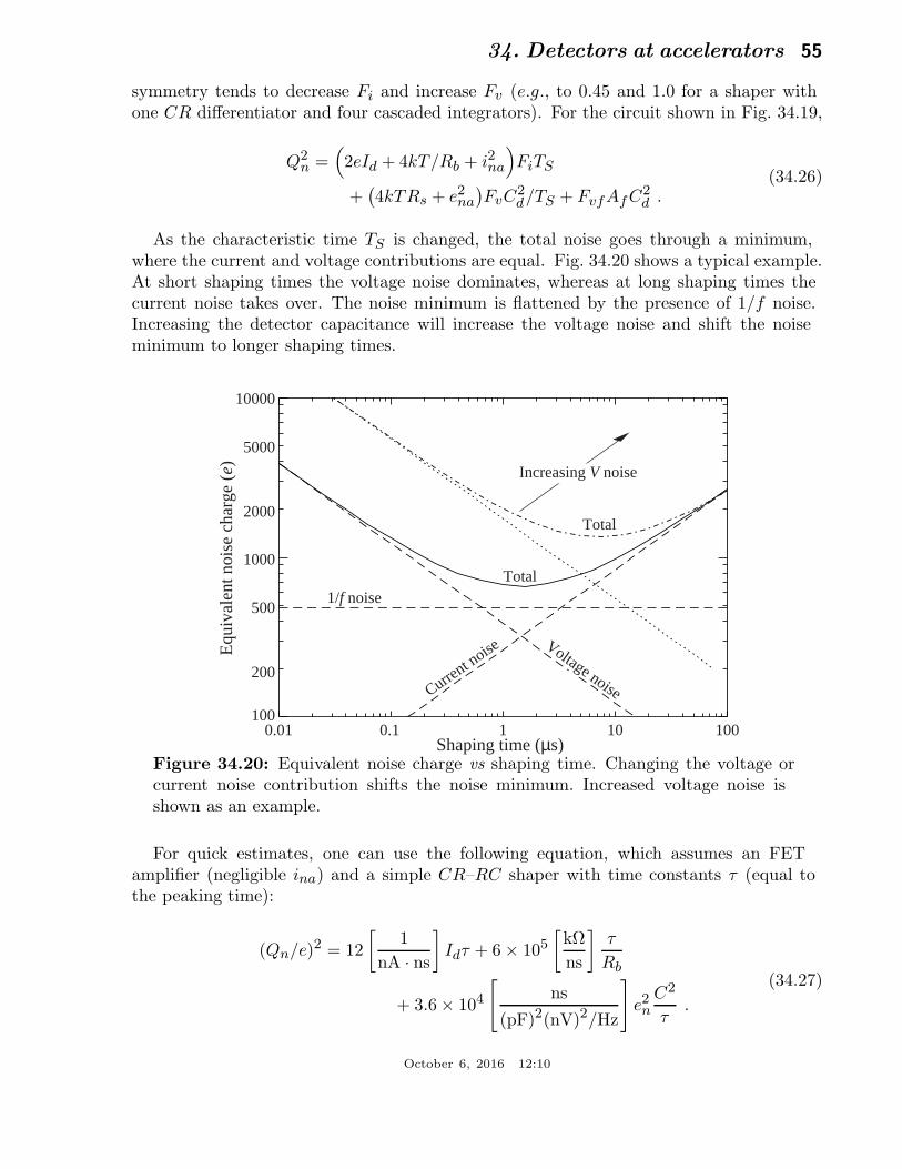
34. Detectors at accelerators 55
symmetry tends to decrease Fi and increase Fv (e.g., to 0.45 and 1.0 for a shaper withone CR differentiator and four cascaded integrators). For the circuit shown in Fig. 34.19,
Q2n =
(
2eId + 4kT/Rb + i2na
)
FiTS
+(
4kTRs + e2na
)
FvC2d/TS + FvfAfC2
d .(34.26)
As the characteristic time TS is changed, the total noise goes through a minimum,where the current and voltage contributions are equal. Fig. 34.20 shows a typical example.At short shaping times the voltage noise dominates, whereas at long shaping times thecurrent noise takes over. The noise minimum is flattened by the presence of 1/f noise.Increasing the detector capacitance will increase the voltage noise and shift the noiseminimum to longer shaping times.
Equ
ival
ent n
oise
cha
rge
(e)
10000
5000
2000
1000
100
500
200
10.10.01 10 100Shaping time (µs)
1/f noise
Current n
oise Voltage noise
Total
Total
Increasing V noise
Figure 34.20: Equivalent noise charge vs shaping time. Changing the voltage orcurrent noise contribution shifts the noise minimum. Increased voltage noise isshown as an example.
For quick estimates, one can use the following equation, which assumes an FETamplifier (negligible ina) and a simple CR–RC shaper with time constants τ (equal tothe peaking time):
(Qn/e)2 = 12
[
1
nA · ns
]
Idτ + 6 × 10⁵[
kΩ
ns
]
τ
Rb
+ 3.6 × 10⁴
[
ns
(pF)2(nV)2/Hz
]
e2n
C2
τ.
(34.27)
October 6, 2016 12:10
56 34. Detectors at accelerators
Noise is improved by reducing the detector capacitance and leakage current, judiciouslyselecting all resistances in the input circuit, and choosing the optimum shaping timeconstant. Another noise contribution to consider is that noise cross-couples from theneighboring front-ends in strip and pixel detectors through the inter-electrode capacitance.
The noise parameters of the amplifier depend primarily on the input device. In fieldeffect transistors, the noise current contribution is very small, so reducing the detectorleakage current and increasing the bias resistance will allow long shaping times withcorrespondingly lower noise. In bipolar transistors, the base current sets a lower bound onthe noise current, so these devices are best at short shaping times. In special cases wherethe noise of a transistor scales with geometry, i.e., decreasing noise voltage with increasinginput capacitance, the lowest noise is obtained when the input capacitance of thetransistor is equal to the detector capacitance, albeit at the expense of power dissipation.Capacitive matching is useful with field-effect transistors, but not bipolar transistors. Inbipolar transistors, the minimum obtainable noise is independent of shaping time, butonly at the optimum collector current IC , which does depend on shaping time.
Q2n,min = 4kT
C√βDC
√
FiFv at Ic =kT
eC
√
βDC
√
Fv
Fi
1
TS, (34.28)
where βDC is the DC current gain. For a CR–RC shaper and βDC = 100,
Qn,min/e ≈ 250√
C/pF . (34.29)
Practical noise levels range from ∼ 1e for CCD’s at long shaping times to ∼ 104 ein high-capacitance liquid argon calorimeters. Silicon strip detectors typically operateat ∼ 103 electrons, whereas pixel detectors with fast readout provide noise of severalhundred electrons.
In timing measurements, the slope-to-noise ratio must be optimized, rather than thesignal-to-noise ratio alone, so the rise time tr of the pulse is important. The “jitter” σt ofthe timing distribution is
σt =σn
(dS/dt)ST
≈ trS/N
, (34.30)
where σn is the rms noise and the derivative of the signal dS/dt is evaluated at the triggerlevel ST . To increase dS/dt without incurring excessive noise, the amplifier bandwidthshould match the rise-time of the detector signal. The 10 to 90% rise time of an amplifierwith bandwidth fU is 0.35/fU . For example, an oscilloscope with 350 MHz bandwidthhas a 1 ns rise time. When amplifiers are cascaded, which is invariably necessary, theindividual rise times add in quadrature.
tr ≈√
t2r1 + t2r2 + ... + t2rn . (34.31)
Increasing signal-to-noise ratio also improves time resolution, so minimizing the totalcapacitance at the input is also important. At high signal-to-noise ratios, the timejitter can be much smaller than the rise time. The timing distribution may shift with
October 6, 2016 12:10

34. Detectors at accelerators 57
signal level (“walk”), but this can be corrected by various means, either in hardware orsoftware [8].
The basic principles discussed above apply to both analog and digital signal processing.In digital signal processing the pulse shaper shown in Fig. 34.18 is replaced by ananalog to digital converter (ADC) followed by a digital processor that determines thepulse shape. Digital signal processing allows great flexibility in implementing filteringfunctions. The software can be changed readily to adapt to a wide variety of operatingconditions and it is possible to implement filters that are impractical or even impossibleusing analog circuitry. However, this comes at the expense of increased circuit complexityand increased demands on the ADC compared to analog shaping.
If the sampling rate of the ADC is too low, high frequency components will betransferred to lower frequencies (“aliasing”). The sampling rate of the ADC must behigh enough to capture the maximum frequency component of the input signal. Apartfrom missing information on the fast components of the pulse, undersampling introducesspurious artifacts. If the frequency range of the input signal is much greater, the noise atthe higher frequencies will be transferred to lower frequencies and increase the noise levelin the frequency range of pulses formed in the subsequent digital shaper. The Nyquistcriterion states that the sampling frequency must be at least twice the maximum relevantinput frequency. This requires that the bandwith of the circuitry preceding the ADCmust be limited. The most reliable technique is to insert a low-pass filter.
The digitization process also introduces inherent noise, since the voltage range ∆Vcorresponding to a minimum bit introduces quasi-random fluctuations relative to theexact amplitude
σn =∆V√
12. (34.32)
When the Nyquist condition is fulfilled the noise bandwidth ∆fn is spread nearlyuniformly and extends to 1/2 the sampling frequency fS , so the spectral noise density
en =σn√∆fn
=∆V√
12· 1√
fS/2=
∆V√6fS
. (34.33)
Sampling at a higher frequency spreads the total noise over a larger frequency range, sooversampling can be used to increase the effective resolution. In practice, this quantizationnoise is increased by differential nonlinearity. Furthermore, the equivalent input noise ofADCs is often rather high, so the overall gain of the stages preceding the ADC must besufficiently large for the preamplifier input noise to override.
When implemented properly, digital signal processing provides significant advantagesin systems where the shape of detector signal pulses changes greatly, for example inlarge semiconductor detectors for gamma rays or in gaseous detectors (e.g. TPCs)where the duration of the current pulse varies with drift time, which can range overorders of magnitude. Where is analog signal processing best (most efficient)? In systemsthat require fast time response the high power requirements of high-speed ADCs areprohibitive. Systems that are not sensitive to pulse shape can use fixed shaper constantsand rather simple filters, which can be either continuous or sampled. In high density
October 6, 2016 12:10
58 34. Detectors at accelerators
systems that require small circuit area and low power (e.g. strip and pixel detectors),analog filtering often yields the required response and tends to be most efficient.
It is important to consider that additional noise is often introduced by externalelectronics, e.g. power supplies and digital systems. External noise can couple to theinput. Often the “common grounding” allows additional noise current to couple tothe current loop connecting the detector to the preamp. Recognizing additional noisesources and minimizing cross-coupling to the detector current loop is often important.Understanding basic physics and its practical effects is important in forming a broad viewof the detector system and recognizing potential problems (e.g. modified data), ratherthan merely following standard recipes.
For a more detailed introduction to detector signal processing and electronics seeRef. 140 or the tutorial website http://www-physics.lbl.gov/ spieler.
34.9. Calorimeters
A calorimeter is designed to measure a particle’s (or jet’s) energy and direction foran (ideally) contained electromagnetic (EM) or hadronic shower. The characteristicinteraction distance for an electromagnetic interaction is the radiation length X0, whichranges from 13.8 g cm−2 in iron to 6.0 g cm−2 in uranium.* Similarly, the characteristicnuclear interaction length λI varies from 132.1 g cm−2 (Fe) to 209 g cm−2 (U).† In eithercase, a calorimeter must be many interaction lengths deep, where “many” is determinedby physical size, cost, and other factors. EM calorimeters tend to be 15–30 X0 deep,while hadronic calorimeters are usually compromised at 5–8 λI . In real experiments thereis likely to be an EM calorimeter in front of the hadronic section, which in turn has lesssampling density in the back, so the hadronic cascade occurs in a succession of differentstructures.
In all cases there is a premium on small λI/ρ and X0/ρ (both with units of length).These quantities are shown for Z > 20 for the chemical elements in Fig. 34.21. For thehadronic case, metallic absorbers in the W–Au region are best, followed by U. The Ru–Pdregion elements are rare and expensive. Lead is a bad choice. Given cost considerations,Fe and Cu might be appropriate choices. For EM calorimeters high Z is preferred, andlead is not a bad choice.
These considerations are for sampling calorimeters consisting of metallic absorbersandwiched or (threaded) with an active material which generates signal. The activemedium may be a scintillator, an ionizing noble liquid, a gas chamber, a semiconductor,or a Cherenkov radiator. The average interaction length is thus greater than that of theabsorber alone, sometimes substantially so.
There are also homogeneous calorimeters, in which the entire volume is sensitive,i.e., contributes signal. Homogeneous calorimeters (so far usually electromagnetic)may be built with inorganic heavy (high density, high 〈Z〉) scintillating crystals, ornon-scintillating Cherenkov radiators such as lead glass and lead fluoride. Scintillation
* X0 = 120 g cm−2 Z−2/3 to better than 5% for Z > 23.† λI = 37.8 g cm−2 A0.312 to within 0.8% for Z > 15.
See pdg.lbl.gov/AtomicNuclearProperties for actual values.
October 6, 2016 12:10

34. Detectors at accelerators 59
20 30 50 70 9040 60 80 100Z
10
0
20
30
40
50
1
0
2
3
4
5
ΛI/
ρ (
cm)
ΛI
X0/
ρ (
cm)
X0
CuFe Ru Pd W Au Pb U
Figure 34.21: Nuclear interaction length λI/ρ (circles) and radiation length X0/ρ(+’s) in cm for the chemical elements with Z > 20 and λI < 50 cm.
light and/or ionization in noble liquids can be detected. Nuclear interaction lengths ininorganic crystals range from 17.8 cm (LuAlO3) to 42.2 cm (NaI). Popular choices havebeen BGO with λI = 22.3 cm and X0 = 1.12 cm, and PbWO4 (20.3 cm and 0.89 cm).Properties of these and other commonly used inorganic crystal scintillators can be foundin Table 34.4.
34.9.1. Electromagnetic calorimeters :Revised September 2015 by R.-Y. Zhu (California Institute of Technology).
The development of electromagnetic showers is discussed in the section on “Passageof Particles Through Matter” (Sec. 33 of this Review). Formulae are given whichapproximately describe average showers, but since the physics of electromagnetic showersis well understood, detailed and reliable Monte Carlo simulation is possible. EGS4 [150]and GEANT [151] have emerged as the standards.
There are homogeneous and sampling electromagnetic calorimeters. In a homogeneouscalorimeter the entire volume is sensitive, i.e., contributes signal. Homogeneouselectromagnetic calorimeters may be built with inorganic heavy (high-Z) scintillatingcrystals such as BaF2, BGO, CsI, LYSO, NaI and PWO, non-scintillating Cherenkovradiators such as lead glass and lead fluoride (PbF2), or ionizing noble liquids. Propertiesof commonly used inorganic crystal scintillators can be found in Table 34.4. A samplingcalorimeter consists of an active medium which generates signal and a passive mediumwhich functions as an absorber. The active medium may be a scintillator, an ionizingnoble liquid, a semiconductor, or a gas chamber. The passive medium is usually amaterial of high density, such as lead, tungsten, iron, copper, or depleted uranium.
The energy resolution σE/E of a calorimeter can be parameterized as a/√
E ⊕ b⊕ c/E,
October 6, 2016 12:10

60 34. Detectors at accelerators
where ⊕ represents addition in quadrature and E is in GeV. The stochastic terma represents statistics-related fluctuations such as intrinsic shower fluctuations,photoelectron statistics, dead material at the front of the calorimeter, and samplingfluctuations. For a fixed number of radiation lengths, the stochastic term a for a samplingcalorimeter is expected to be proportional to
√
t/f , where t is plate thickness and fis sampling fraction [152,153]. While a is at a few percent level for a homogeneouscalorimeter, it is typically 10% for sampling calorimeters.
The main contributions to the systematic, or constant, term b are detector non-uniformity and calibration uncertainty. In the case of the hadronic cascades discussedbelow, non-compensation also contributes to the constant term. One additionalcontribution to the constant term for calorimeters built for modern high-energy physicsexperiments, operated in a high-beam intensity environment, is radiation damage of theactive medium. This can be mitigated by developing radiation-hard active media [51],by reducing the signal path length [52] and by frequent in situ calibration andmonitoring [50,153]. With effort, the constant term b can be reduced to below onepercent. The term c is due to electronic noise summed over readout channels within afew Moliere radii. The best energy resolution for electromagnetic shower measurement isobtained in total absorption homogeneous calorimeters, e.g. calorimeters built with heavycrystal scintillators. These are used when ultimate performance is pursued.
The position resolution depends on the effective Moliere radius and the transversegranularity of the calorimeter. Like the energy resolution, it can be factored as a/
√E ⊕ b,
where a is a few to 20 mm and b can be as small as a fraction of mm for a densecalorimeter with fine granularity. Electromagnetic calorimeters may also provide directionmeasurement for electrons and photons. This is important for photon-related physicswhen there are uncertainties in event origin, since photons do not leave information inthe particle tracking system. Typical photon angular resolution is about 45 mrad/
√E,
which can be provided by implementing longitudinal segmentation [154] for a samplingcalorimeter or by adding a preshower detector [155] for a homogeneous calorimeterwithout longitudinal segmentation.
Novel technologies have been developed for electromagnetic calorimetry. New heavycrystal scintillators, such as PWO and LYSO:Ce (see Sec. 34.4), have attracted muchattention. In some cases, such as PWO, it has received broad applications in high-energyand nuclear physics experiments. The “spaghetti” structure has been developed forsampling calorimetry with scintillating fibers as the sensitive medium. The “shashlik”structure has been developed for sampling calorimetry with wavelength shifting fibersfunctioning as both the converter and transporter for light generated in the sensitivemedium. The “accordion” structure has been developed for sampling calorimetry withionizing noble liquid as the sensitive medium.
Table 34.8 provides a brief description of typical electromagnetic calorimeters builtrecently for high-energy physics experiments. Also listed in this table are calorimeterdepths in radiation lengths (X0) and the achieved energy resolution. Whenever possible,the performance of calorimeters in situ is quoted, which is usually in good agreementwith prototype test beam results as well as EGS or GEANT simulations, provided thatall systematic effects are properly included. Detailed references on detector design and
October 6, 2016 12:10

34. Detectors at accelerators 61
performance can be found in Appendix C of reference [153] and Proceedings of theInternational Conference series on Calorimetry in High Energy Physics.
Table 34.8: Resolution of typical electromagnetic calorimeters. E is in GeV.
Technology (Experiment) Depth Energy resolution Date
NaI(Tl) (Crystal Ball) 20X0 2.7%/E1/4 1983
Bi4Ge3O12 (BGO) (L3) 22X0 2%/√
E ⊕ 0.7% 1993
CsI (KTeV) 27X0 2%/√
E ⊕ 0.45% 1996
CsI(Tl) (BaBar) 16–18X0 2.3%/E1/4 ⊕ 1.4% 1999
CsI(Tl) (BELLE) 16X0 1.7% for Eγ > 3.5 GeV 1998
PbWO4 (PWO) (CMS) 25X0 3%/√
E ⊕ 0.5% ⊕ 0.2/E 1997
Lead glass (OPAL) 20.5X0 5%/√
E 1990
Liquid Kr (NA48) 27X0 3.2%/√
E⊕ 0.42% ⊕ 0.09/E 1998
Scintillator/depleted U 20–30X0 18%/√
E 1988
(ZEUS)
Scintillator/Pb (CDF) 18X0 13.5%/√
E 1988
Scintillator fiber/Pb 15X0 5.7%/√
E ⊕ 0.6% 1995
spaghetti (KLOE)
Liquid Ar/Pb (NA31) 27X0 7.5%/√
E ⊕ 0.5% ⊕ 0.1/E 1988
Liquid Ar/Pb (SLD) 21X0 8%/√
E 1993
Liquid Ar/Pb (H1) 20–30X0 12%/√
E ⊕ 1% 1998
Liquid Ar/depl. U (DØ) 20.5X0 16%/√
E ⊕ 0.3% ⊕ 0.3/E 1993
Liquid Ar/Pb accordion 25X0 10%/√
E ⊕ 0.4% ⊕ 0.3/E 1996
(ATLAS)
October 6, 2016 12:10

62 34. Detectors at accelerators
34.9.2. Hadronic calorimeters : [1–5,153]Revised September 2013 by D. E. Groom (LBNL).
Hadronic calorimetry is considerably more difficult than EM calorimetry. For the samecascade containment fraction discussed in the previous section, the calorimeter wouldneed to be ∼30 times deeper. Electromagnetic energy deposit from the decay of a smallnumber of π0’s are usually detected with greater efficiency than are the hadronic parts ofthe cascade, themselves subject to large fluctuations in neutron production, undetectableenergy loss to nuclear disassociation, and other effects.
Most large hadron calorimeters are parts of large 4π detectors at colliding beamfacilities. At present these are sampling calorimeters: plates of absorber (Fe, Pb, Cu,or occasionally U or W) alternating with plastic scintillators (plates, tiles, bars), liquidargon (LAr), or gaseous detectors. The ionization is measured directly, as in LArcalorimeters, or via scintillation light observed by photodetectors (usually PMT’s orsilicon photodiodes). Wavelength-shifting fibers are often used to solve difficult problemsof geometry and light collection uniformity. Silicon sensors are being studied for ILCdetectors; in this case e-h pairs are collected. There are as many variants of theseschemes as there are calorimeters, including variations in geometry of the absorber andsensors, e.g., scintillating fibers threading an absorber [156], and the “accordion” LArdetector [157]. The latter has zig-zag absorber plates to minimize channeling effects; thecalorimeter is hermitic (no cracks), and plates are oriented so that cascades cross thesame plate repeatedly. Another departure from the traditional sandwich structure is theLAr-tube design shown in Fig. 34.22(a) [158].
(a) (b)
W (Cu) absorber
LAr filledtubes
Hadrons z
rφ
scintillatortile
waveshifter fiber
PMT
Hadrons
Figure 34.22: (a) ATLAS forward hadronic calorimeter structure (FCal2, 3) [158].Tubes containing LAr are embedded in a mainly tungsten matrix. (b) ATLAScentral calorimeter wedge; iron with plastic scintillator tile with wavelength-shiftingfiber readout [159].
A relatively new variant in hadron calorimetry is the detection of Cerenkov light. Such
October 6, 2016 12:10

34. Detectors at accelerators 63
a calorimeter is sensitive to relativistic e±’s in the EM showers plus a few relativisticpions. An example is the radiation-hard forward calorimeter in CMS, with iron absorberand quartz fiber readout by PMT’s [160].
Ideally the calorimeter is segmented in φ and θ (or η = − ln tan(θ/2)). Finesegmentation, while desirable, is limited by cost, readout complexity, practical geometry,and the transverse size of the cascades—but see Ref. 161. An example, a wedge of theATLAS central barrel calorimeter, is shown in Fig. 34.22(b) [159].
Much of the following discussion assumes an idealized calorimeter, with the samestructure throughout and without leakage. “Real” calorimeters usually have an EMdetector in front and a coarse “catcher” in the back. Complete containment is generallyimpractical.
In an inelastic hadronic collision a significant fraction fem of the energy is removedfrom further hadronic interaction by the production of secondary π0’s and η’s, whosedecay photons generate high-energy electromagnetic (EM) showers. Charged secondaries(π±, p, . . . ) deposit energy via ionization and excitation, but also interact with nuclei,producing spallation protons and neutrons, evaporation neutrons, and spallation products.The charged collision products produce detectable ionization, as do the showering γ-raysfrom the prompt de-excitation of highly excited nuclei. The recoiling nuclei generatelittle or no detectable signal. The neutrons lose kinetic energy in elastic collisions,thermalize on a time scale of several µs, and are captured, with the production of moreγ-rays—usually outside the acceptance gate of the electronics. Between endothermicspallation losses, nuclear recoils, and late neutron capture, a significant fraction ofthe hadronic energy (20%–40%, depending on the absorber and energy of the incidentparticle) is used to overcome nuclear binding energies and is therefore lost or “invisible.”
In contrast to EM showers, hadronic cascade processes are characterized by theproduction of relatively few high-energy particles. The lost energy and fem are highlyvariable from event to event. Until there is event-by-event knowledge of both the EMfraction and the invisible energy loss, the energy resolution of a hadron calorimeter willremain significantly worse than that of its EM counterpart.
The efficiency e with which EM deposit is detected varies from event to event, butbecause of the large multiplicity in EM showers the variation is small. In contrast,because a variable fraction of the hadronic energy deposit is detectable, the efficiency hwith which hadronic energy is detected is subject to considerably larger fluctuations. Itthus makes sense to consider the ratio h/e as a stochastic variable.
Most energy deposit is by very low-energy electrons and charged hadrons. Because somany generations are involved in a high-energy cascade, the hadron spectra in a givenmaterial are essentially independent of energy except for overall normalization [163]. Forthis reason 〈h/e〉 is a robust concept, independently of hadron energy and species.
If the detection efficiency for the EM sector is e and that for the hadronic sector is h,then the ratio of the mean response to a pion relative to that for an electron is
〈π/e〉 = 〈fem〉 + 〈fh〉〈h/e〉∗ = 1 − (1 − 〈h/e〉)〈fh〉 (34.34)
It has been shown by a simple induction argument and verified by experiment, that the
∗ Technically, we should write 〈fh(h/e)〉, but we approximate it as 〈fh〉〈h/e〉 to facilitate
October 6, 2016 12:10
64 34. Detectors at accelerators
decrease in the average value of the hadronic energy fraction 〈fh〉 = 1 − 〈fem〉 as theprojectile energy E increases is fairly well described by the power law [162,163]
〈fh〉 ≈ (E/E0)m−1 (for E > E0) , (34.35)
at least up to a few hundred GeV. The exponent m depends logarithmically on the meanmultiplicity and the mean fractional loss to π0 production in a single interaction. It is inthe range 0.80–0.87. E0, roughly the energy for the onset of inelastic collisions, is 1 GeVor a little less for incident pions [162]. Both m and E0 must be obtained experimentallyfor a given calorimeter configuration.
Only the product (1 − 〈h/e〉)E1−m0 can be obtained by measuring 〈π/e〉 as a function
of energy. Since 1 − m is small and E0 ≈ 1 GeV for pion-induced cascades, this fact isusually ignored and 〈h/e〉 is reported.
In a hadron-nucleus collision a large fraction of the incident energy is carried by a“leading particle” with the same quark content as the incident hadron. If the projectileis a charged pion, the leading particle is usually a pion, which can be neutral and hencecontributes to the EM sector. This is not true for incident protons. The result is anincreased mean hadronic fraction for incident protons: E0 ≈ 2.6 GeV [162–165].
By definition, 0 ≤ fem ≤ 1. Its variance σ2fem
changes only slowly with energy, but
perforce 〈fem〉 → 1 as the projectile energy increases. An empirical power law (unrelatedto Eq. (34.34)) of the form σfem = (E/E1)
1−ℓ (where ℓ < 1) describes the energydependence of the variance adequately and has the right asymptotic properties [153].For 〈h/e〉 6= 1 (noncompensation), fluctuations in fem significantly contribute to or evendominate the resolution. Since the fem distribution has a high-energy tail, the calorimeterresponse is non-Gaussian with a high-energy tail if 〈h/e〉 < 1. Noncompensation thusseriously degrades resolution and produces a nonlinear response.
It is clearly desirable to compensate the response, i.e., to design the calorimeter suchthat 〈h/e〉 = 1. This is possible only with a sampling calorimeter, where several variablescan be chosen or tuned:1. Decrease the EM sensitivity. EM cross sections increase with Z,† and most of the
energy in an EM shower is deposited by low-energy electrons. A disproportionatefraction of the EM energy is thus deposited in the higher-Z absorber. Lower-Zcladding, such as the steel cladding on ZEUS U plates, preferentially absorbslow-energy γ’s in EM showers and thus also lowers the electronic response. G10 signalboards in the DØ calorimeters and G10 next to slicon readout detectors has the sameeffect. The degree of EM signal suppression can be somewhat controlled by tuning thesensor/absorber thickness ratio.
2. Increase the hadronic sensitivity. The abundant neutrons produced in the cascadehave large n-p elastic scattering cross sections, so that low-energy scattered protonsare produced in hydrogenous sampling materials such as butane-filled proportionalcounters or plastic scintillator. (The maximal fractional energy loss when a neutron
the rest of the discussion.† The asymptotic pair-production cross section scales roughly as Z0.75, and |dE/dx|
slowly decreases with increasing Z.
October 6, 2016 12:10

34. Detectors at accelerators 65
scatters from a nucleus with mass number A is 4A/(1 + A)2.) The down side inthe scintillator case is that the signal from a highly-ionizing stopping proton can bereduced by as much as 90% by recombination and quenching parameterized by Birks’Law (Eq. (34.2)).
3. Fabjan and Willis proposed that the additional signal generated in the aftermath offission in 238U absorber plates should compensate nuclear fluctuations [166]. Theproduction of fission fragments due to fast n capture was later observed [167].However, while a very large amount of energy is released, it is mostly carried bylow-velocity, very highly ionizing fission fragments which produce very little observablesignal because of recombination and quenching. But in fact much of the compensationobserved with the ZEUS 238U/scintillator calorimeter was mainly the result of methods1 and 2 above.Motivated very much by the work of Brau, Gabriel, Bruckmann, and Wigmans [168],
several groups built calorimeters which were very nearly compensating. The degree ofcompensation was sensitive to the acceptance gate width, and so could be somewhatfurther tuned. These includeda) HELIOS with 2.5 mm thick scintillator plates sandwiched between 2 mm thick 238U
plates (one of several structures); σ/E = 0.34/√
E was obtained,b) ZEUS, 2.6 cm thick scintillator plates between 3.3 mm 238U plates; σ/E = 0.35/
√E,
c) a ZEUS prototype with 10 mm Pb plates and 2.5 mm scintillator sheets;σ/E = 0.44/
√E, and
d) DØ, where the sandwich cell consists of a 4–6 mm thick 238U plate, 2.3 mm LAr, aG-10 signal board, and another 2.3 mm LAr gap; σ/E ≈ 0.45/
√E.
Given geometrical and cost constraints, the calorimeters used in modern collider detectorsare not compensating: 〈h/e〉 ≈ 0.7, for the ATLAS central barrel calorimeter, is typical.
A more versatile approach to compensation is provided by a dual-readout calorimeter,in which the signal is sensed by two readout systems with highly contrasting 〈h/e〉.Although the concept is more than two decades old [169], it was only recently beenimplemented by the DREAM collaboration [170]. The test beam calorimeter consistedof copper tubes, each filled with scintillator and quartz fibers. If the two signals C andS (quartz and scintillator) are both normalized to electron response, then for each eventEq. (34.34) takes the form
C = E[fem + 〈h/e〉|C(1 − fem)]
S = E[fem + 〈h/e〉|S(1 − fem)] (34.36)
for the Cherenkov and scintillator responses. On a dotplot of C/E vs S/E, eventsscatter about a line-segment locus described in Fig. 34.23. With increasing energy thedistribution moves upward along the locus and becomes tighter. Equations 34.36 arelinear in 1/E and fem, and are easily solved to obtain estimators of the corrected energyand fem for each event. Both are subject to resolution effects, but contributions dueto fluctuations in fem are eliminated. The solution for the corrected energy is givenby [163]:
E =ξS − C
ξ − 1, where ξ =
1 − 〈h/e〉|C1 − 〈h/e〉|S
(34.37)
October 6, 2016 12:10

66 34. Detectors at accelerators
0.0 0.2 0.4 0.6 0.8 1.0S/E
0.0
0.2
0.4
0.6
0.8
1.0
C/E
100 GeV MC
Incident γIncident π−
fem = 0
fem = 1
h/e S
h/e C
1 − h/e C
1 − h/e S
Slope ξ =
Figure 34.23: Dotplot of Monte Carlo C (Cherenkov) vs S (scintillator) signals forindividual events in a dual readout calorimeter. Hadronic (π−) induced events areshown in blue, and scatter about the indicated event locus. Electromagnetic eventscluster about (C,S) = (0,0). In this case worse resolution (fewer p.e.’s) was assumedfor the Cherenkov events, leading to the “elliptical” distribution.
ξ is the energy-independent slope of the event locus on a plot of C vs S. It can be foundeither from the fitted slope or by measuring π/e as a function of E. Because we have noknowledge of h/e on an event-by-event basis, it has been replaced by 〈h/e〉 in Eq. (34.37).ξ must be as far from unity as possible to optimize resolution, which means in practicalterms that the scintillator readout of the calorimeter must be as compensating as possible.
Although the usually-dominant contribution of the fem distribution to the resolutioncan be minimized by compensation or the use of dual calorimetry, there remain significantcontributions to the resolution:1. Incomplete corrections for leakage, differences in light collection efficiency, and
electronics calibration.2. Readout transducer shot noise (usually photoelectron statistics), plus electronic noise.3. Sampling fluctuations. Only a small part of the energy deposit takes place in the
scintillator or other sensor, and that fraction is subject to large fluctuations. Thiscan be as high as 40%/
√E (lead/scintillator). It is even greater in the Fe/scint case
because of the very small sampling fraction (if the calorimeter is to be compensating),and substantially lower in a U/scint calorimeter. It is obviously zero for a homogeneouscalorimeter.
4. Intrinisic fluctuations. The many ways ionization can be produced in a hadronicshower have different detection efficiencies and are subject to stochastic fluctuations.In particular, a very large fraction of the hadronic energy (∼20% for Fe/scint, ∼40%
October 6, 2016 12:10

34. Detectors at accelerators 67
for U/scint) is “invisible,” going into nuclear dissociation, thermalized neutrons, etc.The lost fraction depends on readout—it will be greater for a Cherenkov readout, lessfor an organic scintillator readout.Except in a sampling calorimeter especially designed for the purpose, sampling and
intrinsic resolution contributions cannot be separated. This may have been best studiedby Drews et al. [171], who used a calorimeter in which even- and odd-numberedscintillators were separately read out. Sums and differences of the variances were used toseparate sampling and intrinsic contributions.
The fractional energy resolution can be represented by
σ
E=
a1(E)√E
⊕∣
∣
∣
∣
1 −⟨
h
e
⟩∣
∣
∣
∣
(
E
E1
)1−ℓ
(34.38)
The coefficient a1 is expected to have mild energy dependence for a number of reasons.For example, the sampling variance is (π/e)E rather than E. The term (E/E1)
1−ℓ
is the parametrization of σfem discussed above. Usually a plot of (σ/E)2 vs 1/E iawell-described by a straight line (constant a1) with a finite intercept—the square of theright term in Eq. (34.38), is called “the constant term.” Precise data show the slightdownturn [156].
After the first interaction of the incident hadron, the average longitudinal distributionrises to a smooth peak. The peak position increases slowly with energy. The distributionbecomes nearly exponential after several interaction lengths. Examples from the CDHSmagnetized iron-scintillator sandwich calorimeter test beam calibration runs [172] areshown in Fig. 34.24. Proton-induced cascades are somewhat shorter and broader thanpion-induced cascades [165]. A gamma distribution fairly well describes the longitudinaldevelopment of an EM shower, as discussed in Sec. 33.5. Following this logic, Bocket al. suggested that the profile of a hadronic cascade could be fitted by the sum oftwo Γ distributions, one with a characteristic length X0 and the other with lengthλI [173]. Fits to this 4-parameter function are commonly used, e.g., by the ATLASTilecal collaboration [165]. If the interaction point is not known (the usual case), thedistribution must be convoluted with an exponential in the interaction length of theincident particle. Adragna et al. give an analytic form for the convoluted function [165].
The transverse energy deposit is characterized by a central core dominated by EMcascades, together with a wide “skirt” produced by wide-angle hadronic interactions [174].
The CALICE collaboration has tested a “tracking” calorimeter (AHCAL) with highlygranular scintillator readout [161]. Since the position of the first interaction is observed,the average longitudinal and radial shower distributions are obtained.
While the average distributions might be useful in designing a calorimeter, they havelittle meaning for individual events, whose distributions are extremely variable because ofthe small number of particles involved early in the cascade.
Particle identification, primarily e-π discrimination, is accomplished in mostcalorimeters by depth development. An EM shower is mostly contained in 15X0 while ahadronic shower takes about 4λI . In high-A absorbers such as Pb, X0/λI ∼ 0.03. In afiber calorimeter, such as the RD52 dual-readout calorimeter [175], e-π discriminationis achieved by differences in the Cerenkov and scintillation signals, lateral spread, andtiming differences, ultimately achieving about 500:1 discrimination.
October 6, 2016 12:10

68 34. Detectors at accelerators
0 2 4 6 8 101 3 5 7 9
Depth (nuclear interaction lengths)
1
10
100
3
30
300
Sca
led
mea
n nu
mbe
r of
par
ticle
s in
cou
nter
CDHS: 15 GeV 30 GeV 50 GeV 75 GeV100 GeV140 GeV
Figure 34.24: Mean profiles of π+ (mostly) induced cascades in the CDHSneutrino detector [172]. Corresponding results for the ATLAS tile calorimeter canbe found in Ref. 165.
34.9.3. Free electron drift velocities in liquid ionization chambers :Written August 2009 by W. Walkowiak (U. Siegen)
Drift velocities of free electrons in LAr [176] are given as a function of electric fieldstrength for different temperatures of the medium in Fig. 34.25. The drift velocites inLAr have been measured using a double-gridded drift chamber with electrons producedby a laser pulse on a gold-plated cathode. The average temperature gradient of the driftvelocity of the free electrons in LAr is described [176] by
∆vd
∆T vd= (−1.72 ± 0.08) %/K.
Earlier measurements [177–180] used different techniques and show systematic deviationsof the drift velocities for free electrons which cannot be explained by the temperaturedependence mentioned above.
Drift velocities of free electrons in LXe [178] as a function of electric field strengthare also displayed in Fig. 34.25. The drift velocity saturates for |E | > 3 kV/cm, anddecreases with increasing temperature for LXe as well as measured e.g. by [181].
The addition of small concentrations of other molecules like N2, H2 and CH4 in solutionto the liquid typically increases the drift velocities of free electrons above the saturationvalue [178,179], see example for CH4 admixture to LAr in Fig. 34.25. Therefore, actualdrift velocities are critically dependent on even small additions or contaminations.
October 6, 2016 12:10

34. Detectors at accelerators 69
E (kV/cm)
Vd
(m
m/µ
s) 87.0 K 89.8 K 93.9 K
163.0 K
97.0 K
LAr
LAr + 0.5% CH4
LXe
Miller et al. (1968)
Shibamura et al. (1976)Walkowiak (2000)
0 2 4 6 8 10 12 140
1
2
3
4
5
6
7
8
Figure 34.25: Drift velocity of free electrons as a function of electric field strengthfor LAr [176], LAr + 0.5% CH4 [178] and LXe [177]. The average temperaturesof the liquids are indicated. Results of a fit to an empirical function [182] aresuperimposed. In case of LAr at 91 K the error band for the global fit [176] includingstatistical and systematic errors as well as correlations of the data points is given.Only statistical errors are shown for the individual LAr data points.
34.10. Accelerator Neutrino Detectors
Written August 2015 by M.O. Wascko (Imperial College London).
34.10.1. Introduction :Accelerator neutrino experiments span many orders of magnitude in neutrino energy,
from a few MeV to hundreds of GeV. This wide range of neutrino energy is driven bythe many physics applications of accelerator neutrino beams. Foremost among them isneutrino oscillation, which varies as the ratio L/Eν , where L is the neutrino baseline(distance travelled), and Eν is the neutrino energy. But accelerator neutrino beams havealso been used to study the nature of the weak interaction, to probe nucleon form factorsand structure functions, and to study nuclear structure.
The first accelerator neutrino experiment used neutrinos from the decays of high energypions in flight to show that the neutrinos emitted from pion decay are different from theneutrinos emitted by beta decay [183]. The field of accelerator neutrino experiments didnot expand beyond this until Simon van der Meer’s invention of the magnetic focusinghorn [184], which significantly increased the flux of neutrinos aimed toward the detector.In this mini-review, we focus on experiments employing decay-in-flight beams—pions,kaons, charmed mesons, and taus—producing fluxes of neutrinos and antineutrinos from∼ 10 MeV to ∼ 100 GeV.
Neutrino interactions with matter proceed only through the weak interaction, making
October 6, 2016 12:10

70 34. Detectors at accelerators
the cross section extremely small and requiring high fluxes of neutrinos and large detectormasses in order to achieve satisfactory event rates. Therefore, neutrino detector design isa balancing act taking into account sufficient numbers of nuclear targets (often achievedwith inactive detector materials), adequate sampling/segmentation to ensure accuratereconstruction of the tracks and showers produced by neutrino-interaction secondaryparticles, and practical readout systems to allow timely analysis of data.
34.10.2. Signals and Backgrounds :The neutrino interaction processes available increase with increasing neutrino energy
as interaction thresholds are crossed; in general neutrino-interaction cross sections growwith energy; for a detailed discussion of neutrino interactions see [185]. The multiplicityof secondary particles from each interaction process grows in complexity with neutrinoenergy, while the forward-boost due to increasing Eν compresses the occupied phasespace in the lab frame, impacting detector designs. Because decay-in-fight beams produceneutrinos at well-defined times, leading to very small duty factors, the predominantbackgrounds stem from unwanted beam-induced neutrino interactions, i.e. neutrinosinteracting via other processes than the one being studied. This becomes increasinglytrue at high energies because the secondary particles produced by neutrino interactionsyield detector signals that resemble cosmic backgrounds less and less.
Below, we describe a few of the dominant neutrino interaction processes, with a focuson the final state particle content and topologies.
34.10.2.1. Charged-Current Quasi-Elastic Scattering and Pion Production:Below ∼ 2 GeV neutrino energy, the dominant neutrino-nucleus interaction process is
quasi-elastic (QE) scattering. In the charged current (CC) mode, the CCQE base neutrinoreaction is νℓ n → ℓ− p, where ℓ = e, µ, τ , and similarly for antineutrinos, νℓ p → ℓ+ n.The final state particles are a charged lepton, and perhaps a recoiling nucleon if it is givenenough energy to escape the nucleus. Detectors designed to observe this process shouldhave good single-particle track resolution for muon neutrino interactions, but shouldhave good µ/e separation for electron neutrino interactions. Because the interaction crosssection falls sharply with Q2, the lepton typically carries away more of the neutrino’skinetic energy than the recoiling nucleon. The fraction of backward-scattered leptons islarge, however, so detectors with 4π coverage are desirable. The dominant backgroundsin this channel tend to come from single pion production events in which the pion is notdetected.
Near 1 GeV, the quasi-elastic cross section is eclipsed by pion production processes. Atypical single pion production (CC1π) reaction is νℓ n → ℓ− π+ n, but many more finalstate particle combinations are possible. Single pion production proceeds through thecoherent channel and many incoherent processes, dominated by resonance production.With increasing neutrino energy, higher-order resonances can be excited, leading tomultiple pions in the final state. Separating these processes from quasi-elastic scattering,and indeed from each other, requires tagging, and ideally reconstructing, the pions. Sincethese processes can produce neutral pions, electromagnetic (EM) shower reconstructionis more important here than it is for the quasi-elastic channel. The predominantbackgrounds for pion production change with increasing neutrino energy. Detection ofpion processes is also complicated because near threshold the quasi-elastic channel creates
October 6, 2016 12:10
34. Detectors at accelerators 71
pion backgrounds through final state interactions of the recoiling nucleon, and at higherenergies backgrounds come from migration of multiple pion events in which one or morepions is not detected.
34.10.2.2. Deep Inelastic Scattering:Beyond a few GeV, the neutrino has enough energy to probe the nucleon at the parton
scale, leading to deep inelastic scattering (DIS). In the charged-current channel, theDIS neutrino reaction is νℓ N → ℓ− X , where N is a nucleon and X encompasses theentire recoiling hadronic system. The final state particle reconstruction revolves aroundaccurate reconstruction of the lepton momentum and containment and reconstruction ofthe hadronic shower energy. Because of the high neutrino energies involved, DIS eventsare very forward boosted, and can have extremely long particle tracks. For this reason,detectors measuring DIS interactions must be large to contain the hadronic showers inthe detector volume.
34.10.2.3. Neutral Currents:Neutrino interactions proceeding through the neutral current (NC) channel are
identified by the lack of a charged lepton in the final state. For example, the NC elasticreaction is νl N → νl N , and the NC DIS reaction is νl N → νl X . NC interactions aresuppressed relative to CC interactions by a factor involving the weak mixing angle; theprimary backgrounds for NC interactions come from CC interactions in which the chargedlepton is misidentified.
34.10.3. Instances of Neutrino Detector Technology :Below we describe many of the actual detectors that have been built and operated for
use in accelerator neutrino beams.
34.10.3.1. Spark Chambers:In the first accelerator neutrino beam experiment, Lederman, Schwartz, and
Steinberger [183] used an internally-triggered spark chamber detector, filled with 10 tonsof Al planes and surrounded by external scintillator veto planes, to distinguish muontracks from electron showers, and hence muon neutrinos from electron neutrinos. Theinactive Al planes served as the neutrino interaction target and as radiators for EM showerdevelopment. The detector successfully showed the presence of muon tracks from neutrinointeractions. It was also sensitive to the hadronic showers induced by NC interactions,which were unknown at the time. More than a decade later, the Aachen-Padova [186]experiment at CERN also employed an Al spark chamber to detect ∼ 2 GeV neutrinos.
34.10.3.2. Bubble Chambers:Several large bubble chamber detectors were employed as accelerator neutrino detectors
in the 1970s and 80s, performing many of the first studies of the properties of theweak interaction. Bubble chambers provide exquisite granularity in the reconstructionof secondary particles, allowing very accurate separation of interaction processes.However, the extremely slow and labor-intensive acquisition and analysis of the datafrom photographic film led to them being phased out in favor of electronically read outdetectors.
The Gargamelle [187] detector at CERN used Freon and propane gas targets to makethe first observation of neutrino-induced NC interactions and more. The BEBC [188]
October 6, 2016 12:10

72 34. Detectors at accelerators
detector at CERN was a bubble chamber that was alternately filled with liquid hydrogen,deuterium, and a neon-hydrogen mixture; BEBC was also outfitted with a track-sensitivedetector to improve event tagging, and sometimes used with a small emulsion chamber.The SKAT [192] heavy freon bubble chamber was exposed to wideband neutrino andantineutrino beams at the Serpukhov laboratory in the former Soviet Union. A series ofAmerican bubble chambers in the 1970’s and 1980’s made measurements on free nucleonsthat are still crucial inputs for neutrino-nucleus scattering predictions. The 12-footbubble chamber at ANL [189] in the USA used both deuterium and hydrogen targets, asdid the 7-foot bubble chamber at BNL [190]. Fermilab’s 15 foot bubble chamber [191]used deuterium and heavy neon targets.
34.10.3.3. Iron Tracking Calorimeters:Because of the forward boost of high energy interactions, long detectors made of
magnetized iron interspersed with active detector layers have been very successfullyemployed. The long magnetized detectors allow measurements of the momentumof penetrating muons. The iron planes also act as shower-inducing layers, allowingseparation of EM and hadronic showers; the large number of iron planes provide enoughmass for high statistics and/or shower containment. Magnetized iron spectrometers havebeen used for studies of the weak interaction, measurements of structure functions,and searches for neutrino oscillation. Non-magnetized iron detectors have also beensuccessfully employed as neutrino monitors for oscillation experiments and also forneutrino-nucleus interaction studies.
The CDHS [201] detector used layers of magnetized iron modules interspersed withwire drift chambers, with a total (fiducial) mass of 1250 t (750 t), to detector neutrinosin the range 30–300 GeV. Within each iron module, 5 cm (or 15 cm) iron plates wereinterspersed with scintillation counters. The FNAL Lab-E neutrino detector was usedby the CCFR [202] and NuTeV [203] collaborations to perform a series of experimentsin the Fermilab high energy neutrino beam (50 GeV< Eν < 300 GeV). The detectorwas comprised of six iron target calorimeter modules, with 690 t total target mass,followed by three muon spectrometer modules, followed by two drift chambers. Eachiron target calorimeter module comprised 5.2 cm thick steel plates interspersed withliquid scintillation counters and drift chambers. The muon spectrometer was comprisedof toroidal iron magnets interleaved with drift chambers. The MINOS [204] detectors, anear detector of 980 t at FNAL and a far detector of 5400 t in the Soudan mine, arefunctionally identical magnetized iron calorimeters, comprised of iron plates interleavedwith layers of 4 cm wide plastic scintillator strips in alternating orientations. TheT2K [222] on-axis detector, INGRID, consists of 16 non-magnetized iron scintillatorsandwich detectors, each with nine 6.5 cm iron plane (7.1 t total) interspersed betweenlayers of 5 cm wide plastic scintillator strips readout out by multi-pixel photon counters(MPPCs) coupled to WLS fibers. Fourteen of the INGRID modules are arranged in across-hair configuration centered on the neutrino beam axis.
October 6, 2016 12:10
34. Detectors at accelerators 73
34.10.3.4. Cherenkov Detectors:Open volume water Cherenkov detectors were originally built to search for proton
decay. Large volumes of ultra-pure water were lined with photomultipliers to collectCherenkov light emitted by the passage of relativistic charged particles. See Sec. 35.3.1for a detailed discussion of deep liquid detectors for rare processes.
When used to detect ∼ GeV neutrinos, the detector medium acts as a naturalfilter for final state particles below the Cherenkov threshold; this feature has beenexploited successfully by the K2K, MiniBooNE (using mineral oil instead of water), andT2K neutrino oscillation experiments. However, at higher energies Cherenkov detectorsbecome less accurate because the overlapping rings from many final state particles becomeincreasingly difficult to resolve.
The second-generation Cherenkov detector in Japan, Super-Kamiokande [193]( Super-K), comprises 50 kt (22.5 kt fiducial) of water viewed by 11,146 50 cm photomultipliertubes, giving 40% photocathode coverage; it is surrounded by an outer detector regionviewed by 1,885 20 cm photomultipliers. Super-K is the far detector for K2K and T2K,and is described in greater detail elsewhere in this review. The K2K experiment alsoemployed a 1 kt water Cherenkov detector in the suite of near detectors [194], with690 photomultipliers (40% photocathode coverage) viewing the detector volume. TheMiniBooNE detector at FNAL was a 0.8 kt [195] mineral oil Cherenkov detector, with1,520 20 cm photomultipliers (10% photocathode coverage) surrounded by a veto detectorwith 240 20 cm photomultipliers.
34.10.3.5. Scintillation Detectors:Liquid and solid scintillator detectors also employ fully (or nearly fully) active detector
media. Typically organic scintillators, which emit into the ultraviolet range, are dissolvedin mineral oil or plastic and read out by photomultipliers coupled to wavelength shifters(WLS). Open volume scintillation detectors lined with photomultipliers are conceptuallysimilar to Cherenkov detectors, although energy reconstruction is calorimetric in natureas opposed to kinematic (see also Sec. 35.3.1). For higher energies and higher particlemultiplicities, it becomes beneficial to use segmented detectors to help distinguish particletracks and showers from each other.
The LSND [197] detector at LANL was an open volume liquid scintillator detector(of mass 167 t) employed to detect relatively low energy (<300 MeV) neutrinos.The NOνA [200] detectors use segmented volumes of liquid scintillator in which thescintillation light is collected by WLS fibers in the segments that are coupled to avalanchephotodiodes (APDs) at the ends of the volumes. The NOνA far detector, located in AshRiver, MN, is comprised of 896 layers of 15.6 m long extruded PVC scintillator cellsfor a total mass of 14 kt; the NOνA near detector is comprised of 214 layers of 4.1 mscintillator volumes for a total mass of of 300 t. Both are placed in the NuMI beamlineat 0.8 off-axis. The SciBar (Scintillation Bar) detector was originally built for K2Kat KEK in Japan and then re-used for SciBooNE [198] at FNAL. SciBar used plasticscintillator strips with 1.5 cm×2.5 cm rectangular cross section, read out by multianodephotomultipliers (MAPMTs) coupled to WLS fibers, arranged in alternating horizontaland vertical layers, with a total mass of 15 t. Both SciBooNE and K2K employed anEM calorimeter downstream of SciBar and a muon range detector (MRD) downstream
October 6, 2016 12:10

74 34. Detectors at accelerators
of that. The MINERvA [199] detector, in the NuMI beam at FNAL, utilizes a centraltracker comprising 8.3 t of plastic scintillator strips with triangular cross section, andis also read out by MAPMTs coupled to WLS fibers. MINERvA employs several moresubsystems and is described more fully below.
34.10.3.6. Liquid Argon Time Projection Chambers:Liquid argon time projection chambers (LAr-TPCs) were conceived in the 1970s as a
way to achieve a fully active detector with sub-centimeter track reconstruction [205]. Amassive volume of purified liquid argon is put under a strong electric field (hundreds ofV/cm), so that the liberated electrons from the paths of ionizing particles can be driftedto the edge of the volume and read out, directly by collecting charge from wire planesor non-destructively through charge induction in the wire planes. A dual-phase readoutmethod is also being developed, in which the charge is drifted vertically and then passedthrough an amplification region inside a gas volume above the liquid volume; the bottomof the liquid volume is equipped with a PMT array for detecting scintillation photons formthe liquid argon. The first large scale LAr-TPC was the ICARUS T-600 module [206],comprising 760 t of liquid argon with a charge drift length of 1.5 m read out by wires with3 mm pitch, which operated in LNGS, both standalone and also exposed to the CNGShigh energy neutrino beam. The ArgoNeuT [207] detector at FNAL, with fiducial mass25 kg of argon read out with 4 mm pitch wires, was exposed to the NuMI neutrino andantineutrino beams. The MicroBooNE [208] detector at FNAL comprises 170 t of liquidAr, read out with 3 mm wire pitch, which began collecting data in the Booster NeutrinoBeam Oct 2015. A LAr-TPC has also been chosen as the detector design for the futureDUNE neutrino oscillation experiment, from FNAL to Sanford Underground ResearchFacility; both single and dual phase modules are planned.
34.10.3.7. Emulsion Detectors:Photographic film emulsions have been employed in particle physics experiments since
the 1940s [209]. Thanks to advances in scanning technology and automation [213],they have been successfully employed as neutrino detectors. Emulsions are used forexperiments observing CC tau neutrino interactions, where the short lifetime of the tau,ττ = 2.90 × 10⁻¹³s, leading to the short mean path length, c × τ = 87µm, requiresextremely precise track resolution. They are employed in hybrid detectors in which theemulsion bricks are embedded inside fine-grained tracker detectors. In the data analysis,the tracker data are used to select events with characteristics typical of a tau decayin the final state, such as missing energy and unbalanced transverse momentum. Thereconstructed tracks are projected back into an emulsion brick and used as the searchseed for a neutrino interaction vertex.
E531 [210] at Fermilab tested many of the emulsion-tracker hybrid techniques employedby later neutrino experiments, in a detector with approximately 9 kg of emulsion target.The CHORUS [211] experiment at CERN used 1,600 kg of emulsion, in a hybrid detectorwith a fiber tracker, high resolution calorimeter, and muon spectrometer, to search forνµ → ντ oscillation. The DONuT [212] experiment at FNAL used a hybrid detector,with 260 kg of emulsion bricks interspersed with fiber trackers, followed by a magneticspectrometer, and calorimeter, to make the first direct observation of tau neutrino CCinteractions. More recently, the OPERA [214,215,216] experiment used an automated
October 6, 2016 12:10

34. Detectors at accelerators 75
hybrid emulsion detector, with 1,300 t of emulsion, to make the first direct observation ofthe appearance of ντ in a νµ beam.
34.10.3.8. Hybrid Detectors:The CHARM detector [217] at CERN was built to study neutral-current interactions
and search for muon neutrino oscillation. It was a fine-grained ionization calorimetertracker with approximately 150 t of marble as neutrino target, surrounded by a magnetizediron muon system for tagging high angle muons, and followed downstream by a muonspectrometer. The CHARM II detector [218] at CERN comprised a target calorimeterfollowed by a downstream muon spectrometer. Each target calorimeter module consistsof a 4.8 cm thick glass plate followed by a layer of plastic streamer tubes, with spacing1 cm, instrumented with 2 cm wide pickup strips. Every fifth module is followed by a3 cm thick scintillator layer. The total mass of the target calorimeter was 692 t.
The Brookhaven E-734 [219] detector was a tracking calorimeter made up of 172 tliquid scintillator modules interspersed with proportional drift tubes, followed by adense EM calorimeter and a muon spectrometer downstream of that. The detector wasexposed to a wideband horn-focused beam with peak neutrino energy near 1 GeV. TheBrookhaven E-776 [220] experiment comprised a finely segmented EM calorimeter, with2.54 cm concrete absorbers interspersed with planes of drift tubes and acrylic scintillationcounters, with total mass 240 t, followed by a muon spectrometer.
The NOMAD [221] detector at CERN consisted of central tracker detector inside a0.4 T dipole magnet (the magnet was originally used by the UA1 experiment at CERN)followed by a hadronic calorimeter and muon detectors downstream of the magnet. Themain neutrino target is 3 t of drift chambers followed downstream by transition radiationdetectors which are followed by an EM calorimeter. NOMAD was exposed to the samewideband neutrino beam as was CHORUS.
MINERvA, introduced above, is, in its entirety, a hybrid detector, based around acentral plastic scintillator tracker. The scintillator tracker is surrounded by electromag-netic and hadronic calorimetry, which is achieved by interleaving thin lead (steel) layersbetween the scintillator layers for the ECAL (HCAL). MINERvA is situated upstream ofthe MINOS near detector which acts as a muon spectrometer. Upstream of the scintillatortracker is a nuclear target region containing inactive layers of C (graphite), Pb, Fe(steel), and O (water). MINERvA’s physics goals span a wide range of neutrino-nucleusinteraction studies, from form factors to nuclear effects.
T2K [222] in Japan employs two near detectors at 280 m from the neutrino beamtarget, one centered on the axis of the horn-focused J-PARC neutrino beam and oneplaced 2.5 off-axis. The on-axis detector, INGRID, is described above. The 2.5 off-axisdetector, ND280, employs the UA1 magnet (at 0.2 T) previously used by NOMAD. Insidethe magnet volume are three separate detector systems: the trackers, the Pi0 Detector(P0D), and several ECal modules. The tracker detectors comprise two fine-grainedscintillator detectors (FGDs), read out by MPPCs coupled to WLS fibers, interleavedbetween three gas TPCs read out by micromegas planes. The downstream FGD containsinactive water layers in addition to the scintillators. Upstream of the tracker is theP0D, a sampling tracker calorimeter with active detector materials comprising plasticscintillator read out by MPPCs and WLS fibers, and inactive sheets of brass radiators and
October 6, 2016 12:10

76 34. Detectors at accelerators
refillable water modules. Surrounding the tracker and P0D, but still inside the magnet,are lead-scintillator EM sampling calorimeters.
34.11. Superconducting magnets for collider detectors
Revised September 2015 by Y. Makida (KEK)
34.11.1. Solenoid Magnets : In all cases SI unit are assumed, so that the magneticfield, B, is in Tesla, the stored energy, E, is in joules, the dimensions are in meters, andµ0 = 4π × 10−7.
The magnetic field (B) in an ideal solenoid with a flux return iron yoke, in which themagnetic field is < 2 T, is given by
B =µ0 n I
L(34.39)
where n is the number of turns, I is the current and L is the coil length. In an air-coresolenoid, the central field is given by
B(0, 0) = µ0 n IL√
L2 + 4R2, (34.40)
where R is the coil radius.In most cases, momentum analysis is made by measuring the circular trajectory of the
passing particles according to p = mv = qrB, where p is the momentum, m the mass, qthe charge, r the bending radius. The sagitta, s, of the trajectory is given by
s = q B ℓ2/8p , (34.41)
where ℓ is the path length in the magnetic field. In a practical momentum measurementin colliding beam detectors, it is more effective to increase the magnetic volume than thefield strength, since
dp/p ∝ p/B ℓ2 , (34.42)
where ℓ corresponds to the solenoid coil radius R. The energy stored in the magneticfield of any magnet is calculated by integrating B2 over all space:
E =1
2µ0
∫
B2dV (34.43)
If the coil thin and inside an iron return yoke , (which is the case if it is to superconductingcoil), then
E ≈ (B2/2µ0)πR2L . (34.44)
For a detector in which the calorimetry is outside the aperture of the solenoid, the coilmust be thin in terms of radiation and absorption lengths. This usually means thatthe coil is superconducting and that the vacuum vessel encasing it is of minimum real
October 6, 2016 12:10

34. Detectors at accelerators 77
Table 34.9: Progress of superconducting magnets for particle physics detectors.
Experiment Laboratory B Radius Length Energy X/X0 E/M[T] [m] [m] [MJ] [kJ/kg]
TOPAZ* KEK 1.2 1.45 5.4 20 0.70 4.3CDF* Tsukuba/Fermi 1.5 1.5 5.07 30 0.84 5.4VENUS* KEK 0.75 1.75 5.64 12 0.52 2.8AMY* KEK 3 1.29 3 40 †CLEO-II* Cornell 1.5 1.55 3.8 25 2.5 3.7ALEPH* Saclay/CERN 1.5 2.75 7.0 130 2.0 5.5DELPHI* RAL/CERN 1.2 2.8 7.4 109 1.7 4.2ZEUS* INFN/DESY 1.8 1.5 2.85 11 0.9 5.5H1* RAL/DESY 1.2 2.8 5.75 120 1.8 4.8BaBar* INFN/SLAC 1.5 1.5 3.46 27 † 3.6D0* Fermi 2.0 0.6 2.73 5.6 0.9 3.7BELLE* KEK 1.5 1.8 4 42 † 5.3BES-III IHEP 1.0 1.475 3.5 9.5 † 2.6ATLAS-CS ATLAS/CERN 2.0 1.25 5.3 38 0.66 7.0ATLAS-BT ATLAS/CERN 1 4.7–9.75 26 1080 (Toroid)†
ATLAS-ET ATLAS/CERN 1 0.825–5.35 5 2 × 250 (Toroid)†
CMS CMS/CERN 4 6 12.5 2600 † 12SiD** ILC 5 2.9 5.6 1560 † 12ILD** ILC 4 3.8 7.5 2300 † 13SiD** CLIC 5 2.8 6.2 2300 † 14ILD** CLIC 4 3.8 7.9 2300 †FCC** 6 6 23 54000 † 12
∗ No longer in service∗∗Conceptual design in future† EM calorimeter is inside solenoid, so small X/X0 is not a goal
thickness and fabricated of a material with long radiation length. There are two majorcontributors to the thickness of a thin solenoid:1) The conductor consisting of the current-carrying superconducting material (usually
Nb-Ti/Cu) and the quench protecting stabilizer (usually aluminum) are wound on theinside of a structural support cylinder (usually aluminum also). The coil thicknessscales as B2R, so the thickness in radiation lengths (X0) is
tcoil/X0 = (R/σhX0)(B2/2µ0) , (34.45)
where tcoil is the physical thickness of the coil, X0 the average radiation length of thecoil/stabilizer material, and σh is the hoop stress in the coil [225]. B2/2µ0 is themagnetic pressure. In large detector solenoids, the aluminum stabilizer and supportcylinders dominate the thickness; the superconductor (Nb-TI/Cu) contributes a
October 6, 2016 12:10

78 34. Detectors at accelerators
smaller fraction. The main coil and support cylinder components typically contributeabout 2/3 of the total thickness in radiation lengths.
2) Another contribution to the material comes from the outer cylindrical shell of thevacuum vessel. Since this shell is susceptible to buckling collapse, its thickness isdetermined by the diameter, length and the modulus of the material of which it isfabricated. The outer vacuum shell represents about 1/3 of the total thickness inradiation length.
34.11.2. Properties of collider detector magnets :The physical dimensions, central field stored energy and thickness in radiation lengths
normal to the beam line of the superconducting solenoids associated with the majorcollider are given in Table 34.9 [224]. Fig. 34.26 shows thickness in radiation lengths asa function of B2R in various collider detector solenoids.
0
0.5
1
1.5
2
2.5
3
0 1 2 3 4 5 6 7 8
Thi
ckne
ss in
rad
iatio
n le
ngth
s
B2R [T2m]
ZEUS
VENUS
BESS,WASA
ALEPH
H1
DELPHI
TOPAZ CDF
D0
CLEO-II
SSC-SDCprototype
ATLAS-CSCELLO
PEP4-TPC
Figure 34.26: Magnet wall thickness in radiation length as a function of B2R forvarious detector solenoids. Gray entries are for magnets no longer in use, and entriesunderlined are not listed in Table 34.9. Open circles are for magnets not designedto be “thin.” The SSC-SDC prototype provided important R&D for LHC magnets.
The ratio of stored energy to cold mass (E/M) is a useful performance measure. Itcan also be expressed as the ratio of the stress, σh, to twice the equivalent density, ρ, inthe coil [225]:
E
M=
E
ρ 2πtcoilRL≈ σh
2ρ(34.46)
The E/M ratio in the coil is approximately equivalent to H,* the enthalpy of the coil,
* The enthalpy, or heat content, is called H in the thermodynamics literature. It is not
October 6, 2016 12:10

34. Detectors at accelerators 79
and it determines the average coil temperature rise after energy absorption in a quench:
E/M = H(T2) − H(T1) ≈ H(T2) (34.47)
where T2 is the average coil temperature after the full energy absorption in a quench,and T1 is the initial temperature. E/M ratios of 5, 10, and 20 kJ/kg correspond to ∼65,∼80, and ∼100 K, respectively. The E/M ratios of various detector magnets are shownin Fig. 34.27 as a function of total stored energy. One would like the cold mass to beas small as possible to minimize the thickness, but temperature rise during a quenchmust also be minimized. An E/M ratio as large as 12 kJ/kg is designed into the CMSsolenoid, with the possibility that about half of the stored energy can go to an externaldump resistor. Thus the coil temperature can be kept below 80 K if the energy extractionsystem works well. The limit is set by the maximum temperature that the coil design cantolerate during a quench. This maximum local temperature should be <130 K (50 K +80 K), so that thermal expansion effects, which are remarkable beyond 80 K, in the coilare manageable less than 50 K.
0
5
10
15
1 10 100 1000 104
E/M
[k
J/k
g]
Stored Energy [MJ]
D0
ZEUS
VENUS
BABAR
CDF
BELLE DELPHI
ALEPH
H1
CMS
BES-III
(CLIC-SiD)
(ILC-ILD)
(ILC-SiD)
TOPAZ
CLEO-II
ATLAS-CS
SSC-SDCPrototype
Figure 34.27: Ratio of stored energy to cold mass for major detector solenoids.Gray indicates magnets no longer in operation.
to be confused with the magnetic field intensity B/µ.
October 6, 2016 12:10

80 34. Detectors at accelerators
34.11.3. Toroidal magnets :Toroidal coils uniquely provide a closed magnetic field without the necessity of an iron
flux-return yoke. Because no field exists at the collision point and along the beam line,there is, in principle, no effect on the beam. On the other hand, the field profile generallyhas 1/r dependence. The particle momentum may be determined by measurements ofthe deflection angle combined with the sagitta. The deflection (bending) power BL is
BL ≈∫ R0
Ri
BiRi dR
R sin θ=
Bi Ri
sin θln(R0/Ri) , (34.48)
where Ri is the inner coil radius, R0 is the outer coil radius, and θ is the angle betweenthe particle trajectory and the beam line axis . The momentum resolution given by thedeflection may be expressed as
∆p
p∝ p
BL≈ p sin θ
BiRi ln(R0/Ri). (34.49)
The momentum resolution is better in the forward/backward (smaller θ) direction. Thegeometry has been found to be optimal when R0/Ri ≈ 3–4. In practical designs, the coilis divided into 6–12 lumped coils in order to have reasonable acceptance and accessibility.This causes the coil design to be much more complex. The mechanical structure needs tosustain the decentering force between adjacent coils, and the peak field in the coil is 3–5times higher than the useful magnetic field for the momentum analysis [223].
34.12. Measurement of particle momenta in a uniform magnetic
field [226,227]
The trajectory of a particle with momentum p (in GeV/c) and charge ze in a constantmagnetic field
−→B is a helix, with radius of curvature R and pitch angle λ. The radius of
curvature and momentum component perpendicular to−→B are related by
p cos λ = 0.3 z B R , (34.50)where B is in tesla and R is in meters.
The distribution of measurements of the curvature k ≡ 1/R is approximately Gaussian.The curvature error for a large number of uniformly spaced measurements on thetrajectory of a charged particle in a uniform magnetic field can be approximated by
(δk)2 = (δkres)2 + (δkms)
2 , (34.51)where δk = curvature error
δkres = curvature error due to finite measurement resolutionδkms = curvature error due to multiple scattering.
If many (≥ 10) uniformly spaced position measurements are made along a trajectoryin a uniform medium,
δkres =ǫ
L′ 2
√
720
N + 4, (34.52)
where N = number of points measured along track
October 6, 2016 12:10

34. Detectors at accelerators 81
L′ = the projected length of the track onto the bending planeǫ = measurement error for each point, perpendicular to the trajectory.
If a vertex constraint is applied at the origin of the track, the coefficient under the radicalbecomes 320.
For arbitrary spacing of coordinates si measured along the projected trajectory andwith variable measurement errors ǫi the curvature error δkres is calculated from:
(δkres)2 =
4
w
Vss
VssVs2s2 − (Vss2)2, (34.53)
where V are covariances defined as Vsmsn = 〈smsn〉 − 〈sm〉〈sn〉 with 〈sm〉 =w−1 ∑
(sim/ǫi
2) and w =∑
ǫi−2.
The contribution due to multiple Coulomb scattering is approximately
δkms ≈(0.016)(GeV/c)z
Lpβ cos2 λ
√
L
X0, (34.54)
where p = momentum (GeV/c)z = charge of incident particle in units of eL = the total track length
X0 = radiation length of the scattering medium (in units of length; the X0 definedelsewhere must be multiplied by density)
β = the kinematic variable v/c.
More accurate approximations for multiple scattering may be found in the section onPassage of Particles Through Matter (Sec. 33 of this Review). The contribution to thecurvature error is given approximately by δkms ≈ 8srms
plane/L2, where srmsplane is defined
there.
References:
1. T. Ferbel (ed.), Experimental Techniques in High Energy Physics, Addison-Wesley,Menlo Park, CA (1987).
2. K. Kleinknecht, Detectors for Particle Radiation, Cambridge University Press,Cambridge (1998).
3. G.F. Knoll, Radiation Detection and Measurement, 3nd edition, John Wiley &Sons, New York (1999).
4. D.R. Green, The Physics of Particle Detectors, Cambridge Monographs on ParticlePhysics, Nuclear Physics and Cosmology, Cambridge University Press, Cambridge(2000).
5. C. Leroy and P.-G. Rancoita, Principles of Radiation Interaction in Matter andDetection, World Scientific, Singapore (2004).
6. C. Grupen, Particle Detectors, Cambridge Monographs on Particle Physics, NuclearPhysics and Cosmology, Cambridge University Press (2008).
7. ICARUS Collab., ICARUS-TM/2001-09 [LGNS-EXP 13/89 add.2/01] (2001).8. H. Spieler, IEEE Trans. NS29, 1142 (1982).9. K. Arisaka, Nucl. Instrum. Methods A442, 80 (2000).
October 6, 2016 12:10

82 34. Detectors at accelerators
10. T. Hakamata (ed.), Photomultiplier Tubes: Basics and Applications, 3rd edition,Hamamatsu Photonics K.K., Hamamatsu (2006).
11. A. Braem et al., Nucl. Instrum. Methods A518, 574 (2004).12. R. Arnold et al., Nucl. Instrum. Methods A314, 465 (1992).13. P. Mangeot et al., Nucl. Instrum. Methods A216, 79 (1983);
R. Apsimon et al., IEEE Trans. NS33, 112 (1986);R. Arnold et al., Nucl. Instrum. Methods A270, 255 (1988);D. Aston et al., Nucl. Instrum. Methods A283, 582 (1989).
14. J. Janesick, Scientific charge-coupled devices, SPIE Press, Bellingham, WA (2001).15. R. Haitz et al., J. Appl. Phys. 36, 3123 (1965);
R. McIntyre, IEEE Trans. Electron Devices 13, 164 (1966);H. Dautet et al., Applied Optics, 32, 3894 (1993);Perkin-Elmer Optoelectronics, Avalanche Photodiodes: A User’s Guide, (2003).
16. P. Buzhan et al., Nucl. Instrum. Methods A504, 48 (2003);Z. Sadygov et al., Nucl. Instrum. Methods A504, 301 (2003);V. Golovin and V. Saveliev, Nucl. Instrum. Methods A518, 560 (2004).
17. M. Landstrass et al., Diam. & Rel. Matter, 2, 1033 (1993);R. McKeag and R. Jackman, Diam. & Rel. Matter, 7, 513 (1998);R. Brascia et al., Phys. Stat. Sol. 199, 113 (2003).
18. M. Petrov, M. Stapelbroek, and W. Kleinhans, Appl. Phys. Lett. 51, 406 (1987);M. Atac and M. Petrov, IEEE Trans. NS36, 163 (1989);M. Atac et al., Nucl. Instrum. Methods A314, 56 (1994).
19. J.B. Birks, The Theory and Practice of Scintillation Counting, Pergamon, London(1964).
20. D. Clark, Nucl. Instrum. Methods 117, 295 (1974).21. J.B. Birks, Proc. Phys. Soc. A64, 874 (1951).22. B. Bengston and M. Moszynski, Nucl. Instrum. Methods 117, 227 (1974);
J. Bialkowski et al., Nucl. Instrum. Methods 117, 221 (1974).23. C. P. Achenbach, arXiv:nucl-ex/0404008 (2004).24. I.B. Berlman, Handbook of Fluorescence Spectra of Aromatic Molecules, 2nd edition,
Academic Press, New York (1971).25. F. Sauli (ed.), Instrumentation in High Energy Physics, World Scientific, Singapore
(1992), see pp. 218–279 by C. Zorn.26. T. Foerster, Ann. Phys. 2, 55 (1948).27. J.M. Fluornoy, Rad. Phys. and Chem. 41, 389 (1993).28. D. Horstman and U. Holm, Rad. Phys. and Chem. 41, 395 (1993).29. D. Blomker et al., Nucl. Instrum. Methods A311, 505 (1992);
J. Mainusch et al., Nucl. Instrum. Methods A312, 451 (1992).30. K.F. Johnson and R.L. Clough (eds.), Proceedings of the International Conference
on Radiation-Tolerant Plastic Scintillators and Detectors, Rad. Phys. and Chem.41 (1993).
31. S.R. Borenstein and R.C. Strand, IEEE Trans. NS31, 396 (1984).32. P. Sonderegger, Nucl. Instrum. Methods A257, 523 (1987).33. P. Achenbach et al., Nucl. Instrum. Methods A593, 353 (2008).
October 6, 2016 12:10

34. Detectors at accelerators 83
34. C.M. Hawkes et al., Nucl. Instrum. Methods A292, 329 (1990).35. S.E. Derenzo, W.-S. Choong and W.W. Moses, Phys. Med. Biol. 59, 3261 (2014).36. C. Melcher and J. Schweitzer, Nucl. Instrum. Methods A314, 212 (1992).37. D.W. Cooke et al., J. Appl. Phys. 88, 7360 (2000).38. J.M. Chen et al., IEEE Trans. NS54, 718 (2007);
J.M. Chen et al., IEEE Trans. NS54, 1319 (2007).39. E.V.D. van Loef et al., Nucl. Instrum. Methods A486, 254 (2002).40. W. Drozdowski et al., IEEE Trans. NS55, 1391 (2008).41. M.S. Alekhin et al., Appl. Phys. Lett. 102, 161915 (2013).42. C. Kuntner et al., Nucl. Instrum. Methods A493, 131 (2002).43. N. Akchurin et al., Nucl. Instrum. Methods A595, 359 (2008).44. A. Para, FERMILAB-CONF-11-519-CD (2011);
H. Wenzel et al., FERMILAB-PUB-11-531-CD-E (2011).45. R.H. Mao, L.Y. Zhang and R.Y. Zhu, IEEE Trans. NS59, 2229 (2012).46. W.W. Moses, W.-S. Choong and S.E. Derenzo, Acta Physica Polonica B7, 725
(2014).47. R.H. Mao, L.Y. Zhang and R.Y. Zhu, IEEE Trans. NS55, 2425 (2008).48. B.D. Rooney and J.D. Valentine, IEEE Trans. NS44, 509 (1997).49. W.W. Moses et al., IEEE Trans. NS55, 1049 (2008).50. G. Gratta, H. Newman, and R.Y. Zhu, Ann. Rev. Nucl. and Part. Sci. 44, 453
(1994).51. R.Y. Zhu, Nucl. Instrum. Methods A413, 297 (1998).52. R.Y. Zhu, Journal of Physics: Conference Series 587, 012055 (2015).53. G. Dissertori et al., Nucl. Instrum. Methods 745, 1 (2014), and references therein.54. R. Chipaux et al., Proc. of the 8th Int. Conf. on Inorganic Scintillators
(SCINT2005), 369 (2005).55. The CMS Electromagnetic Calorimeter Group, JINST 5 P03010 (2010).56. M.G. Albrow et al., JINST 7, P10027 (2012).57. B. Aubert et al. [BaBar Collab.], Nucl. Instrum. Methods A479, 1 (2002).58. A. Abashian et al., Nucl. Instrum. Methods A479, 117 (2002).59. M. Shiozawa et al. [Super-Kamiokande Collab.], Nucl. Instrum. Methods A433,
240 (1999).60. Proceedings of the International Workshops on Ring Imaging Cherenkov Detectors,
Nucl. Instrum. Methods A343, 1 (1993); Nucl. Instrum. Methods A371, 1 (1996);Nucl. Instrum. Methods A433, 1 (1999); Nucl. Instrum. Methods A502, 1 (2003);Nucl. Instrum. Methods A553, 1 (2005); Nucl. Instrum. Methods A595, 1 (2008);Nucl. Instrum. Methods A639, 1 (2011); Nucl. Instrum. Methods A766, 1 (2014).
61. J. Litt and R. Meunier, Ann. Rev. Nucl. Sci. 23, 1 (1973).62. D. Bartlett et al., Nucl. Instrum. Methods A260, 55 (1987).63. B. Ratcliff, Nucl. Instrum. Methods A502, 211 (2003).64. W. Blum, W. Riegler, and L. Rolandi, Particle Detection with Drift Chambers,
Springer-Verlag, Berlin (2008).65. L.G. Christophorou, Atomic and Molecular Radiation Physics, John Wiley & Sons,
Hoboken (1971);
October 6, 2016 12:10

84 34. Detectors at accelerators
I.B. Smirnov, Nucl. Instrum. Methods A554, 474 (2005);J. Berkowitz, Atomic and Molecular Photoabsorption, Academic Press, Cambridge(2002);http://pdg.lbl.gov/2007/AtomicNuclearProperties.
66. H. Bichsel, Nucl. Instrum. Methods A562, 154 (2006).
67. H. Fischle et al., Nucl. Instrum. Methods A301, 202 (1991).
68. http://rjd.web.cern.ch/rjd/cgi-bin/cross.
69. A. Peisert and F. Sauli, CERN 84-08 (1984).
70. S. Biagi, Nucl. Instrum. Methods A421, 234 (1999).
71. http://consult.cern.ch/writeup/magboltz/.
72. E. McDaniel and E. Mason, The Mobility and Diffusion of Ions in Gases, JohnWiley & Sons, Hoboken (1973);G. Shultz et al., Rev. Phys. Appl. 12, 67 (1977).
73. G. Charpak et al., Nucl. Instrum. Methods A62, 262 (1968).
74. G. Charpak and F. Sauli, Ann. Rev. Nucl. Sci. 34, 285 (1984).
75. T. Ferbel (ed.), Experimental Techniques in High Energy Physics, Addison-Wesley,Menlo Park, CA (1987), see “Principles of Operation of Multiwire Proportionaland Drift Chambers”.
76. G. Charpak et al., Nucl. Instrum. Methods A167, 455 (1979).
77. A.H. Walenta et al., Nucl. Instrum. Methods A92, 373 (1971).
78. A. Breskin et al., Nucl. Instrum. Methods A124, 189 (1975).
79. A. Breskin et al., Nucl. Instrum. Methods A156, 147 (1978).
80. R. Bouclier et al., Nucl. Instrum. Methods A265, 78 (1988).
81. H. Drumm et al., Nucl. Instrum. Methods A176, 333 (1980).
82. D.R. Nygren and J.N. Marx, Phys. Today 31N10, 46 (1978).
83. http://www.ansoft.com.
84. P. Beringer et al., Nucl. Instrum. Methods A254, 542 (1987).
85. J. Virdee, Phys. Reports 403, 401 (2004).
86. H. Walenta, Phys. Scripta 23, 354 (1981).
87. J. Va’vra, Nucl. Instrum. Methods A515, 1 (2003);M. Titov, arXiv:physics/0403055 (2004).
88. M. Aleksa et al., Nucl. Instrum. Methods A446, 435 (2000).
89. F. Sauli and A. Sharma, Ann. Rev. Nucl. Part. Sci. 49, 341 (1999).
90. A. Oed, Nucl. Instrum. Methods A263, 351 (1988);A. Barr et al., Nucl. Phys. (Proc. Supp.) B61, 264 (1988).
91. Y. Bagaturia et al., Nucl. Instrum. Methods A490, 223 (2002).
92. J. Benlloch et al., IEEE Trans. NS45, 234 (1998).
93. Y. Giomataris, Nucl. Instrum. Methods A419, 239 (1998).
94. F. Sauli, Nucl. Instrum. Methods A386, 531 (1997);A. Bressan et al., Nucl. Instrum. Methods A425, 262 (1999).
95. S. Bachmann et al., Nucl. Instrum. Methods A479, 294 (2002);A. Bressan et al., Nucl. Instrum. Methods A424, 321 (1999).
96. Y. Giomataris et al., Nucl. Instrum. Methods A376, 29 (1996).
October 6, 2016 12:10

34. Detectors at accelerators 85
97. J. Derre et al., Nucl. Instrum. Methods A459, 523 (2001);G. Charpak et al., Nucl. Instrum. Methods A478, 26 (2002).
98. I. Giomataris et al., Nucl. Instrum. Methods A560, 405 (2006).99. S. Duarte Pinto et al., IEEE NSS Conf. Record N08-4, 1426 (2008).
100. L. Periale et al., Nucl. Instrum. Methods A478, 377 (2002);R. Chechik et al., Nucl. Instrum. Methods A535, 303 (2004);A. Breskin et al., Nucl. Instrum. Methods A598, 107 (2009).
101. A. Di Mauro et al., Nucl. Instrum. Methods A581, 225 (2007).102. R. Bellazzini et al., Nucl. Instrum. Methods A535, 477 (2004);
M. Campbell et al., Nucl. Instrum. Methods A540, 295 (2005);A. Bamberger et al., Nucl. Instrum. Methods A573, 361 (2007);T.Kim et al., Nucl. Instrum. Methods A599, 173 (2008).
103. M. Chefdeville et al., Nucl. Instrum. Methods A556, 490 (2006).104. M. Titov, arXiv:physics/0403055 (2004).105. http://rd51-public.web.cern.ch/RD51-Public.106. J. Alme et al., Nucl. Instrum. Methods A622, 316 (2010).107. N. Abgrall et al., Nucl. Instrum. Methods A637, 25 (2011).108. ALICE Collab., ALICE-PUBLIC-2015-004 (2015).109. A.H. Walenta et al., Nucl. Instrum. Methods 161, 45 (1979).110. H. Aihara et al., IEEE Trans. NS30, 63 (1983).111. X. Artru et al., Phys. Rev. D12, 1289 (1975);
G.M. Garibian et al., Nucl. Instrum. Methods 125, 133 (1975).112. B. Dolgoshein, Nucl. Instrum. Methods A326, 434 (1993).113. TRDs for the Third Millenium: Proc. 2nd Workshop on Advanced Transition
Radiation Detectors for Accelerator and Space Applications, Nucl. Instrum.Methods A522, 1 (2004).
114. TRDs for the Third Millenium: Proc. 4th Workshop on Advanced TransitionRadiation Detectors for Accelerator and Space Applications, Nucl. Instrum.Methods A706, 1 (2013).
115. B. Beischer et al., Nucl. Instrum. Methods A583, 485 (2007).116. A. Adronic and J.P Wessels, Nucl. Instrum. Methods A666, 130 (2012).117. M. Petris et al., Nucl. Instrum. Methods A714, 17 (2007).118. J. Apostolakis et al., Rad. Phys. and Chem. 78, 859 (2009).119. R. Santonico and R. Cardarelli, Nucl. Instrum. Methods A187, 377 (1981).120. V.V. Parkhomchuck, Yu.N. Pestov, and N.V. Petrovykh, Nucl. Instrum. Methods
93, 269 (1971).121. E. Cerron Zeballos et al., Nucl. Instrum. Methods A374, 132 (1996).122. R. Cardarelli et al., Nucl. Instrum. Methods A333, 399 (1993).123. P. Camarri et al., Nucl. Instrum. Methods A414, 317 (1998).124. G. Aielli et al., Nucl. Instrum. Methods A508, 6 (2003).125. R. Cardarelli et al., Nucl. Instrum. Methods A382, 470 (1996).126. R. Cardarelli et al., JINST 8, P01003 (2013).127. G. Aielli et al., JINST 9, C09030 (2014).128. R. Santonico, JINST 9, C11007 (2014).
October 6, 2016 12:10

86 34. Detectors at accelerators
129. R. Santonico et al., Nucl. Instrum. Methods A661, S2 (2012).
130. M. Bedjidian et al., JINST 6 P02001 (2011).
131. P. Fonte et al., Nucl. Instrum. Methods A443, 201 (2000).
132. L. Paolozzi et al., PoS(RPC2012)065 (2012).
133. S. An et al., Nucl. Instrum. Methods A594, 39 (2008).
134. C. Iacobaeus et al., Nucl. Instrum. Methods A513, 244 (2003).
135. G. Aielli et al., Nucl. Instrum. Methods A456, 82 (2000).
136. G. Aielli et al., IEEE Trans. NS53, 567 (2006).
137. H. Sakai et al., Nucl. Instrum. Methods A484, 153 (2002).
138. R. Santonico, JINST 8, P04023 (2013).
139. L. Lopes et al., Nucl. Instrum. Methods A533, 69 (2003).
140. H. Spieler, Semiconductor Detector Systems, Oxford Univ. Press, Oxford (2005).
141. F. Scholze et al., Nucl. Instrum. Methods A439, 208 (2000).
142. G. Lindstrom et al., Nucl. Instrum. Methods A465, 60 (2001).
143. C. Da Via et al., Nucl. Instrum. Methods A509, 86 (2003).
144. G. Kramberger et al., Nucl. Instrum. Methods A481, 297 (2002).
145. O. Krasel et al., IEEE Trans. NS51, 3055 (2004).
146. G. Lindstrom et al., Nucl. Instrum. Methods A426, 1 (1999).
147. A. Holmes-Siedle and L. Adams, Handbook of Radiation Effects, 2nd edition,Oxford Univ. Press, Oxford (2002).
148. V. Radeka, IEEE Trans. NS15, 455 (1968);V. Radeka, IEEE Trans. NS21, 51 (1974).
149. F.S. Goulding, Nucl. Instrum. Methods 100, 493 (1972);F.S. Goulding and D.A. Landis, IEEE Trans. NS29, 1125 (1982).
150. W.R. Nelson, H. Hirayama, and D.W.O. Rogers, SLAC-265 (1985).
151. R. Brun et al., CERN DD/EE/84-1 (1987).
152. D. Hitlin et al., Nucl. Instrum. Methods 137, 225 (1976);See also W. J. Willis and V. Radeka, Nucl. Instrum. Methods 120, 221 (1974), fora more detailed discussion.
153. R. Wigmans, Calorimetry: Energy Measurement in Particle Physics, Inter. Seriesof Monographs on Phys. 107, Clarendon Press, Oxford (2000).
154. ATLAS Collab., CERN/LHCC 96-41 (1996).
155. CMS Collab., CERN/LHCC 97-33 (1997).
156. N. Akchurin et al., Nucl. Instrum. Methods A399, 202 (1997).
157. B. Aubert et al., Nucl. Instrum. Methods A321, 467 (1992).
158. A. Artamonov et al., JINST 3, P02010 (2008).
159. F. Ariztizabal et al., Nucl. Instrum. Methods A349, 384 (1994).
160. S. Abdullin et al., Eur. Phys. J. C53, 139 (2008).
161. M. Romalli, J. Phys. Conf. Series 404 012050 (2012);C. Adloff et al., arXiv:1306.3037 (2013).
162. T.A. Gabriel et al., Nucl. Instrum. Methods A338, 336 (1994).
163. D.E. Groom, Nucl. Instrum. Methods A572, 633 (2007); Erratum: D.E. Groom,Nucl. Instrum. Methods A593, 638 (2008).
October 6, 2016 12:10

34. Detectors at accelerators 87
164. N. Akchurin et al., Nucl. Instrum. Methods A408, 380 (1998); An energy-independent analysis of these data is given in Ref. 163.
165. P. Adragna et al., Nucl. Instrum. Methods A615, 158 (2010).166. C.W. Fabjan et al., Phys. Lett. B60, 105 (1975).167. C. Leroy, J. Sirois, and R. Wigmans, Nucl. Instrum. Methods A252, 4 (1986).168. J.E. Brau and T.A. Gabriel, Nucl. Instrum. Methods A238, 489 (1985);
H. Bruckmann and H. Kowalski, ZEUS Int. Note 86/026 DESY, Hamburg (1986);R. Wigmans, Nucl. Instrum. Methods A259, 389 (1987);R. Wigmans, Nucl. Instrum. Methods A265, 273 (1988).
169. P. Mockett, SLAC-267, 335 (1987).170. R. Wigmans, Proc. 7th Inter. Conf. on Calorimetry in High Energy Physics, 182
World Scientific, River Edge, NJ, (1998);N. Akchurin et al., Nucl. Instrum. Methods A537, 537 (2005).
171. G. Drews et al., Nucl. Instrum. Methods A335, 335 (1990).172. M. Holder et al., Nucl. Instrum. Methods 151, 69 (1978).173. R.K. Bock, T. Hansl-Kozanecka, and T.P. Shah, Nucl. Instrum. Methods 186, 533
(1981);Y.A. Kulchitsky and V.B. Vinogradov, Nucl. Instrum. Methods A455, 499 (2000).
174. D. Acosta et al., Nucl. Instrum. Methods A316, 184 (1997).175. N. Akchurin, et al., Nucl. Instrum. Methods A735, 120 (2013).176. W. Walkowiak, Nucl. Instrum. Methods A449, 288 (2000).177. L.S. Miller et al., Phys. Rev. 166, 871 (1968).178. E. Shibamura et al., Nucl. Instrum. Methods A316, 184 (1975).179. K. Yoshino et al., Phys. Rev. A14, 438 (1976).180. A.O. Allen et al., NSRDS-NBS-58 (1976).181. P. Benetti et al., Nucl. Instrum. Methods A32, 361 (1993).182. A.M. Kalinin et al., ATLAS-LARG-NO-058 (1996).183. G. Danby et al., Phys. Rev. Lett. 9, 36 (1962).184. S. van der Meer, CERN 61-07 (1961).185. J.A. Formaggio and G.P. Zeller, Rev. Mod. Phys. 84, 1307 (2013).186. H. Faissner et al., Phys. Lett. B68, 377 (1977).187. F.J. Hasert et al., Nucl. Phys. B73, 1 (1974).188. N. Armenise et al., Phys. Lett. B81, 385 (1979).189. S.J. Barish et al., Phys. Rev. D16, 3103 (1977).190. N.J. Baker et al., Phys. Rev. D23, 2499 (1981).191. J.W. Chapman et al., Phys. Rev. D14, 5 (1976).192. A.E. Asratien et al., Phys. Lett. 79, 497 (1978).193. Y. Fukuda et al., Nucl. Instrum. Methods A501, 418 (2003).194. Y. Fukuda et al., Phys. Rev. D74, 072003 (2006).195. A.A. Aguilar-Arevalo et al., Nucl. Instrum. Methods A599, 28 (2009).196. A.A. Aguilar-Arevalo et al., Phys. Rev. D79, 072002 (2009).197. C. Athanassopoulos et al., Nucl. Instrum. Methods A388, 149 (1997).198. K. Hiraide et al., Phys. Rev. D78, 112004 (2008).199. L. Aliaga et al., Nucl. Instrum. Methods A743, 130 (2014).
October 6, 2016 12:10

88 34. Detectors at accelerators
200. D.S. Ayres et al., FERMILAB-DESIGN-2007-01 (2007).201. M. Holder et al., Nucl. Instrum. Methods 148, 203 (1978).202. W.K. Sakumoto et al., Nucl. Instrum. Methods A294, 179 (1990).203. D.A. Harris et al., Nucl. Instrum. Methods A447, 377 (2000).204. I. Ambats et al., FERMILAB-DESIGN-1998-02 (1998).205. C. Rubbia, CERN-EP-INT-77-08 (1977).206. S. Amerio et al., Nucl. Instrum. Methods A527, 329 (2004).207. C. Anderson et al., JINST 7, 10020 (2012).208. H. Chen et al., FERMILAB-PROPOSAL-0974 (2007).209. D.H. Perkins, Nature 159, 126 (1947).210. N. Uhida et al., Nucl. Instrum. Methods 224, 50 (1984).211. S. Aoki et al., Nucl. Instrum. Methods A447, 361 (2000).212. K. Kodama et al., Nucl. Instrum. Methods B93, 340 (1994).213. S. Aoki, Nucl. Instrum. Methods A473, 192 (2001).214. T. Adam et al., Nucl. Instrum. Methods A577, 523 (2007).215. D. Di Ferdinando et al., Radiat. Meas. 44, 840 (2009).216. R. Acquafredda et al., New J. Phys. 8, 303 (2006).217. A.N. Diddens et al., Nucl. Instrum. Methods 178, 27 (1980).218. D. Geiregat et al., Nucl. Instrum. Methods A325, 92 (1993).219. L.A. Ahrens et al., Nucl. Instrum. Methods A254, 515 (1987).220. G. Gidal, LBL-91 Suppl., Rev. (1985).221. J. Altegoer et al., Nucl. Instrum. Methods A404, 96 (1998).222. K. Abe et al., Nucl. Instrum. Methods A659, 106 (2011).223. T. Taylor, Phys. Scripta 23, 459 (1980).224. A. Yamamoto, Nucl. Instrum. Methods A494, 255 (2003).225. A. Yamamoto, Nucl. Instrum. Methods A453, 445 (2000).226. R.L. Gluckstern, Nucl. Instrum. Methods 24, 381 (1963).227. V. Karimaki, Nucl. Instrum. Methods A410, 284 (1998).
October 6, 2016 12:10