3676 ieee transactions on power …pelstechpro.weebly.com/uploads/1/2/8/1/12811276/high...3676 ieee...
TRANSCRIPT
3676 IEEE TRANSACTIONS ON POWER ELECTRONICS, VOL. 27, NO. 8, AUGUST 2012
High Efficiency AC–AC Power Electronic ConverterApplied to Domestic Induction Heating
Hector Sarnago, Member, IEEE, Arturo Mediano, Senior Member, IEEE, and Oscar Lucia, Member, IEEE
Abstract—This paper presents the analysis and design of a newac–ac resonant converter applied to domestic induction heating.The proposed topology, based on the half-bridge series resonantinverter, uses only two diodes to rectify the mains voltage. The pro-posed converter can operate with zero-voltage switching duringboth switch-on and switch-off transitions. Moreover, this topologydoubles the output voltage, and therefore, the current in the load isreduced for the same output power. As a consequence, the converterefficiency is significantly improved. The analytical and simulationresults have been verified by means of a 3600-W induction heat-ing prototype. An efficiency study has been carried out, obtainingvalues higher than 96%.
Index Terms—Home appliances, induction heating, inverters,resonant power conversion.
I. INTRODUCTION
INDUCTION heating appliance market is increasing due toits fastest heating time and efficiency. Domestic induction
hobs are now becoming a standard option, especially in Asiaand Europe.
The principle of operation is based on the generation of avariable magnetic field by means of a planar inductor below ametallic vessel [1], [2]. The mains voltage is rectified and afterthat an inverter provides a medium-frequency current to feed theinductor. The usual operating frequency is higher than 20 kHzto avoid the audible range and lower than 100 kHz to reduceswitching losses. The most used device is the insulated gatebipolar transistor (IGBT) because of the operating frequencyrange and the output power range, up to 3 kW. Nowadays, mostdesigns use the half-bridge series resonant topology because ofits control simplicity and high efficiency [3]–[7].
In the past, several ac–ac topologies have been proposed tosimplify the converter and improve the efficiency [8]–[10]. Con-sidering the induction heating application, several resonant ma-trix converters featuring MOSFETs [11], [12], IGBTs [13], orRB-IGBTs [14], [15] have been proposed. However, the final
Manuscript received June 8, 2011; revised September 7, 2011 and November14, 2011; accepted January 14, 2012. Date of current version April 20, 2012.This work was supported in part by the Spanish Ministerio de Ciencia e In-novacion under Project TEC2010-19207, Project CSD2009-00046, and ProjectIPT-2011-1158-920000 and in part by the Bosch and Siemens Home AppliancesGroup under Grant PTAUZ-2011-TEC-A-004. Recommended for publicationby Associate Editor L. M. Tolbert.
The authors are with the Department of Electronic Engineering and Com-munications, University of Zaragoza, Zaragoza 50009, Spain (e-mail: [email protected]; [email protected]; [email protected]).
Color versions of one or more of the figures in this paper are available onlineat http://ieeexplore.ieee.org.
Digital Object Identifier 10.1109/TPEL.2012.2185067
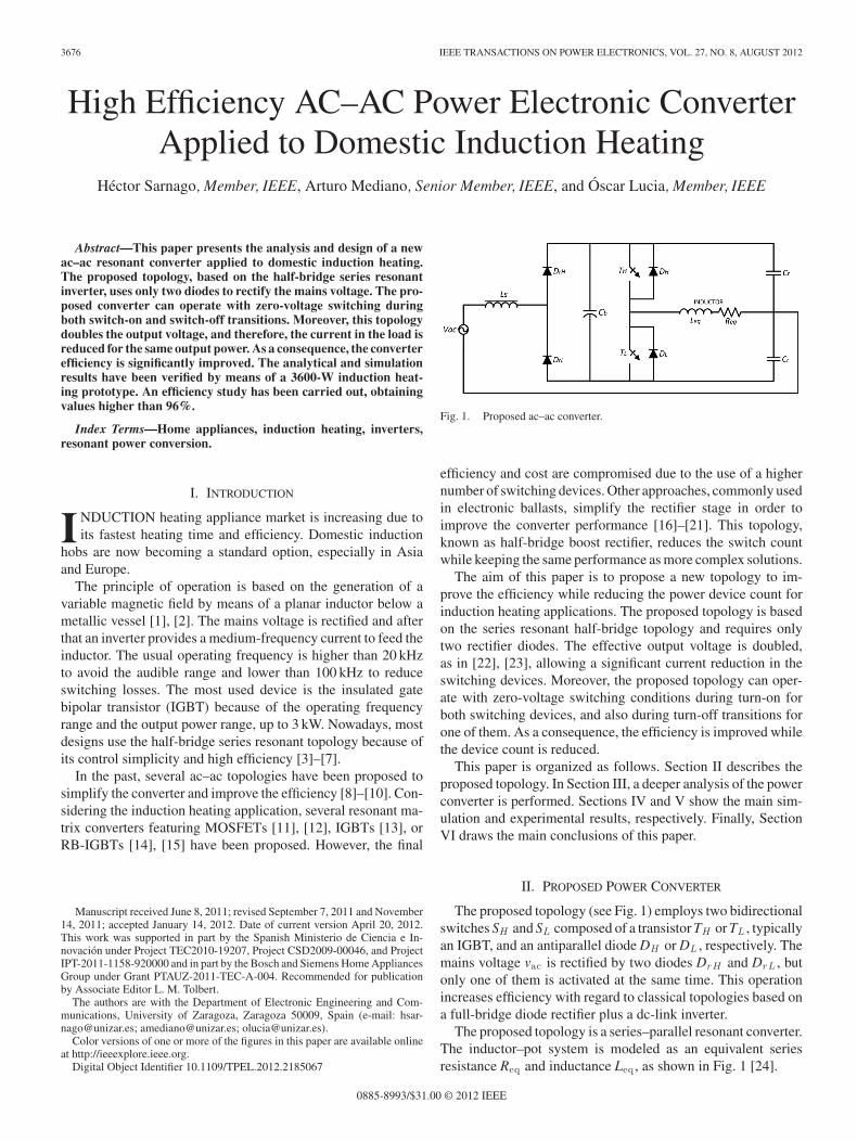
Fig. 1. Proposed ac–ac converter.
efficiency and cost are compromised due to the use of a highernumber of switching devices. Other approaches, commonly usedin electronic ballasts, simplify the rectifier stage in order toimprove the converter performance [16]–[21]. This topology,known as half-bridge boost rectifier, reduces the switch countwhile keeping the same performance as more complex solutions.
The aim of this paper is to propose a new topology to im-prove the efficiency while reducing the power device count forinduction heating applications. The proposed topology is basedon the series resonant half-bridge topology and requires onlytwo rectifier diodes. The effective output voltage is doubled,as in [22], [23], allowing a significant current reduction in theswitching devices. Moreover, the proposed topology can oper-ate with zero-voltage switching conditions during turn-on forboth switching devices, and also during turn-off transitions forone of them. As a consequence, the efficiency is improved whilethe device count is reduced.
This paper is organized as follows. Section II describes theproposed topology. In Section III, a deeper analysis of the powerconverter is performed. Sections IV and V show the main sim-ulation and experimental results, respectively. Finally, SectionVI draws the main conclusions of this paper.
II. PROPOSED POWER CONVERTER
The proposed topology (see Fig. 1) employs two bidirectionalswitches SH and SL composed of a transistor TH or TL , typicallyan IGBT, and an antiparallel diode DH or DL , respectively. Themains voltage vac is rectified by two diodes DrH and DrL , butonly one of them is activated at the same time. This operationincreases efficiency with regard to classical topologies based ona full-bridge diode rectifier plus a dc-link inverter.
The proposed topology is a series–parallel resonant converter.The inductor–pot system is modeled as an equivalent seriesresistance Req and inductance Leq , as shown in Fig. 1 [24].
0885-8993/$31.00 © 2012 IEEE
SARNAGO et al.: HIGH EFFICIENCY AC–AC POWER ELECTRONIC CONVERTER APPLIED TO DOMESTIC INDUCTION HEATING 3677
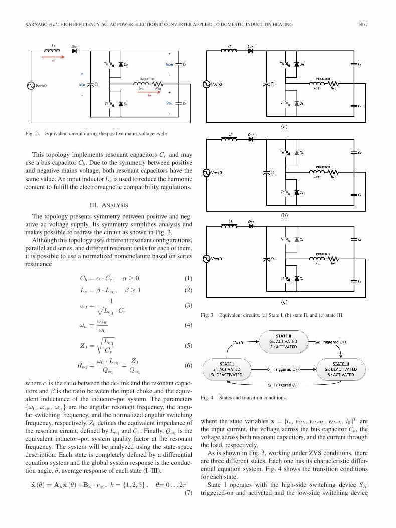
Fig. 2. Equivalent circuit during the positive mains voltage cycle.
This topology implements resonant capacitors Cr and mayuse a bus capacitor Cb . Due to the symmetry between positiveand negative mains voltage, both resonant capacitors have thesame value. An input inductor Ls is used to reduce the harmoniccontent to fulfill the electromagnetic compatibility regulations.
III. ANALYSIS
The topology presents symmetry between positive and neg-ative ac voltage supply. Its symmetry simplifies analysis andmakes possible to redraw the circuit as shown in Fig. 2.
Although this topology uses different resonant configurations,parallel and series, and different resonant tanks for each of them,it is possible to use a normalized nomenclature based on seriesresonance
Cb = α · Cr , α ≥ 0 (1)
Ls = β · Leq , β ≥ 1 (2)
ω0 =1
√Leq · Cr
(3)
ωn =ωsw
ω0(4)
Z0 =√
Leq
Cr(5)
Req =ω0 · Leq
Qeq=
Z0
Qeq(6)
where α is the ratio between the dc-link and the resonant capac-itors and β is the ratio between the input choke and the equiv-alent inductance of the inductor–pot system. The parameters{ω0 , ωsw , ωn} are the angular resonant frequency, the angu-lar switching frequency, and the normalized angular switchingfrequency, respectively. Z0 defines the equivalent impedance ofthe resonant circuit, defined by Leq and Cr . Finally, Qeq is theequivalent inductor–pot system quality factor at the resonantfrequency. The system will be analyzed using the state-spacedescription. Each state is completely defined by a differentialequation system and the global system response is the conduc-tion angle, θ, average response of each state (I–III):
x (θ) = Akx (θ) +Bk · vac , k = {1, 2, 3} , θ= 0 . . . 2π(7)
Fig. 3 Equivalent circuits. (a) State I, (b) state II, and (c) state III.
Fig. 4 States and transition conditions.
where the state variables x = [is , vC b , vC rH , vC rL , i0]T arethe input current, the voltage across the bus capacitor Cb , thevoltage across both resonant capacitors, and the current throughthe load, respectively.
As is shown in Fig. 3, working under ZVS conditions, thereare three different states. Each one has its characteristic differ-ential equation system. Fig. 4 shows the transition conditionsfor each state.
State I operates with the high-side switching device SH
triggered-on and activated and the low-side switching device

3678 IEEE TRANSACTIONS ON POWER ELECTRONICS, VOL. 27, NO. 8, AUGUST 2012
(SL ) triggered-off. The parallel resonant circuit is set by anequivalent capacitor Ceq , obtained from Cr and Cb and ex-pressed in (8), and the inductor electrical parameters, Req andLeq . The current flowing through SH is the same as the oneflowing through the load
Ceq = Cr
(1 +
Cb
Cr + Cb
)= Cr
(1 + 2α1 + α
). (8)
State I begins when SL is triggered OFF. In this moment, theantiparallel diode DH conducts and SH can be triggered ONensuring ZVS switching-on conditions. Transitions from thisstate can lead either to state II or state III. If voltage across SL
reaches zero and DL starts conducting, the transition conditionto state II is fulfilled. On the other hand, if SH is switched OFFwhen TH conducts, the next state is state III.
The normalized differential equations that define the dynam-ics of the system in this state are
di0 (θ)dθ
=1
ωnZ0(vC eq (θ) − Req · i0 (θ)) (9)
dvC eq (θ)dθ
=Z0 (1 + α)ωn (1 + 2α)
(is (θ) + i0 (θ)) (10)
dis (θ)dθ
=1
βωnZ0(vac − vC eq (θ)) . (11)
Therefore, the state-space matrices for state I are
A1 =
⎛
⎜⎜⎜⎜⎜⎜⎜⎜⎜⎜⎜⎜⎜⎜⎜⎝
0 0−1
βωn Z00 0
Z0
ωn (1 + 2α)0 0 0
Z0
ωn (1 + 2α)
Z0 (1 + α)ωn (1 + 2α)α
0 0 0Z0 (1 + α)
ωn (1 + 2α)α
−αZ0
ωn (1 + 2α)0 0 0
−αZ0
ωn (1 + 2α)
01
ωn Z00 0
−Req
ωn Z0
⎞
⎟⎟⎟⎟⎟⎟⎟⎟⎟⎟⎟⎟⎟⎟⎟⎠
B1 =
⎛
⎜⎜⎜⎜⎜⎜⎜⎝
1βωn Z0
0
0
0
0
⎞
⎟⎟⎟⎟⎟⎟⎟⎠
. (12)
State II is characterized by the conduction of both switchingdevices, although only SH is triggered ON. That is, TH and DL
conduct at the same time. Current through load is supplied byboth devices (TH and DL ), and consequently, low conductionstress for the devices is achieved. The equivalent parallel reso-nant circuit is set by the inductor electrical parameters in paral-lel with both resonant capacitors. Cb is short-circuited by bothswitching devices. This state starts when the voltage across SL
reaches zero. At this moment, DL starts conducting at the sametime as TH is triggered ON. This state finishes when SH is trig-gered OFF and the next state is state III. The main benefit resultsof the lower switch-off current achieved when SH is triggered
OFF, due to the fact that the load current is supplied by bothdevices. In addition, SH achieves ZVS conditions during bothswitch-on and switch-off transitions, reducing consequently theswitching losses.
The normalized differential equations that define the dynam-ics of the system in this state are
dis (θ)dθ
=1
βωnZ0(Vs − vC rH (θ)) (13)
vC b = 0 (14)
dvC rH (θ)dθ
=Z0
2ωn(is (θ) + i0 (θ)) (15)
dvC rL (θ)dθ
=−Z0
2ωn(is (θ) + i0 (θ)) (16)
di0 (θ)dθ
=1
ωnZ0(vC rH (θ) − Req · i0 (θ)) . (17)
The state-space matrix for this state is shown in the nextequation
A2 =
⎛
⎜⎜⎜⎜⎜⎜⎜⎜⎜⎜⎜⎜⎜⎝
0 0−1
βωnZ00 0
0 0 0 0 0Z0
2ωn0 0 0
Z0
2ωn
−Z0
2ωn0 0 0
−Z0
2ωn
0 01
ωnZ00
−Req
ωnZ0
⎞
⎟⎟⎟⎟⎟⎟⎟⎟⎟⎟⎟⎟⎟⎠
B2 =
⎛
⎜⎜⎜⎜⎜⎜⎜⎝
1βωnZ0
0
0
0
0
⎞
⎟⎟⎟⎟⎟⎟⎟⎠
. (18)
State III is defined by the conduction of SL while SH is deac-tivated. The equivalent resonant circuit is set by one resonantcapacitor in parallel with the series connection of the Cb capaci-tor and the parallel connection of the inductor and the other oneresonant capacitance. Note that when Cb is zero (α = 0), theequivalent resonant circuit is a series RLC circuit composed ofthe inductor–pot system and one resonant capacitor. This statestarts when SH is triggered OFF. At this moment, DL starts con-ducting and SL can be triggered ON achieving ZVS switch-onconditions. This state finishes when SL is deactivated, and thenext state is state I.
The normalized differential equations system that defines thedynamics is
dis (θ)dθ
=1
βωnZ0(Vs − vC rH (θ)) (19)
dvC b (θ)dθ
=Z0
ωn
(is (θ) − i0 (θ)
2 + α
α
)(20)

SARNAGO et al.: HIGH EFFICIENCY AC–AC POWER ELECTRONIC CONVERTER APPLIED TO DOMESTIC INDUCTION HEATING 3679
dvC rH (θ)dθ
=Z0
ωn(is (θ) (1 + α) − i0 (θ) α) (21)
dvC rL (θ)dθ
=−Z0
ωn(is (θ) α − i0 (θ) (1 + α)) (22)
di0 (θ)dθ
=1
ωnZ0(vC rH (θ) − vC b (θ) − Req · i0 (θ)) . (23)
The space state matrix for this state is shown in the nextequation
A3 =
⎛
⎜⎜⎜⎜⎜⎜⎜⎜⎜⎜⎜⎜⎜⎜⎜⎜⎝
0 0−1
βωnZ00 0
Z0
ωn0 0 0
−Z0 (2 + α)αωn
Z0 (1 + α)ωn
0 0 0−αZ0
ωn
−αZ0
ωn0 0 0
Z0 (1 + α)ωn
0−1
ωnZ0
1ωnZ0
0−Req
ωnZ0
⎞
⎟⎟⎟⎟⎟⎟⎟⎟⎟⎟⎟⎟⎟⎟⎟⎟⎠
B3 =
⎛
⎜⎜⎜⎜⎜⎜⎜⎝
1βωnZ0
0
0
0
0
⎞
⎟⎟⎟⎟⎟⎟⎟⎠
. (24)
IV. SIMULATION RESULTS
By using the space-state analysis presented in Section III,two operating modes can be described (see Fig. 5). Both ofthem achieve ZVS switch-on conditions; however, only the firstoperation mode can achieve the ZVS switch-off conditions forSH . The first operation mode uses the three states describedearlier: I, II, and III. It makes possible to achieve ZVS conditionsfor the high-side switch in state II. The low-side switch has non-ZVS turn-off characteristic. However, turn-off current is alwayslower than in the high-side switch.
The second operation mode only uses two states: I andIII. This operation mode does not achieve ZVS conditionsduring switch-off, and the switching losses are, therefore, in-creased. This switching losses can be reduced by using snubbercapacitors [25], [26].
Nowadays, the induction heating appliances’ power is limitedby mains maximum current and voltage. The typical maximumoutput power is 3600 W, and the power converter prototypehas been, therefore, designed to achieve 3600-W output power.Simulation parameters are Cr = 470 nF, and the inductor ismodeled by Leq = 65 μH and 6.5 Ω for the series-equivalentresistor at switching frequency. The dc-link capacitor has beenselected to be low enough to obtain a high power factor and aproper power control, as it is shown in this section, and it canbe neglected in this analysis.
Fig. 5 Operation modes. (a) First operation mode. (b) Second operation mode.
The control strategies considered to control the output powerare the square wave (SW) control, based on changing the switch-ing frequency, and the asymmetrical duty cycle control [6], [25],[27], based on changing the duty cycle of the switching devices.Next subsections detail the main simulation results.
A. SW Control Review Stage
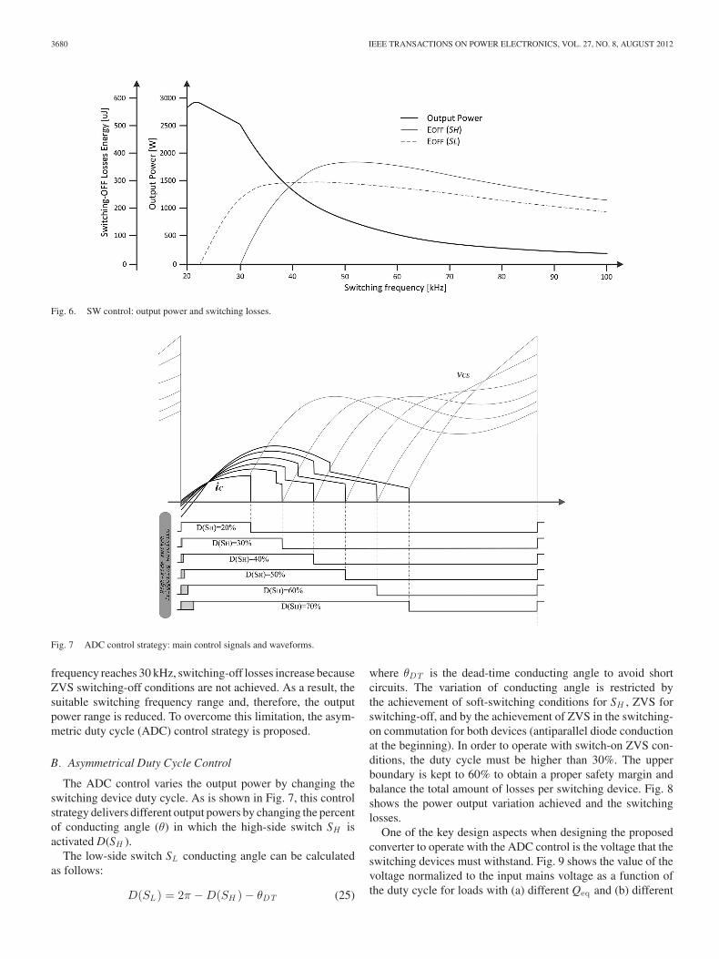
The SW control modifies the output power by controlling theswitching frequency. The switching frequency is higher than theresonant frequency to achieve switch-on ZVS, and the outputpower is reduced when the switching frequency is increased(see Fig. 6).
As is shown in Fig. 6, the frequency range starts at 22 kHz,which is the resonant frequency determined by Leq and Cr ,that ensures ZVS switching-on conditions, and can be in-creased to decrease the output power. However, if the switching
3680 IEEE TRANSACTIONS ON POWER ELECTRONICS, VOL. 27, NO. 8, AUGUST 2012
Fig. 6. SW control: output power and switching losses.
Fig. 7 ADC control strategy: main control signals and waveforms.
frequency reaches 30 kHz, switching-off losses increase becauseZVS switching-off conditions are not achieved. As a result, thesuitable switching frequency range and, therefore, the outputpower range is reduced. To overcome this limitation, the asym-metric duty cycle (ADC) control strategy is proposed.
B. Asymmetrical Duty Cycle Control
The ADC control varies the output power by changing theswitching device duty cycle. As is shown in Fig. 7, this controlstrategy delivers different output powers by changing the percentof conducting angle (θ) in which the high-side switch SH isactivated D(SH ).
The low-side switch SL conducting angle can be calculatedas follows:
D(SL ) = 2π − D(SH ) − θDT (25)
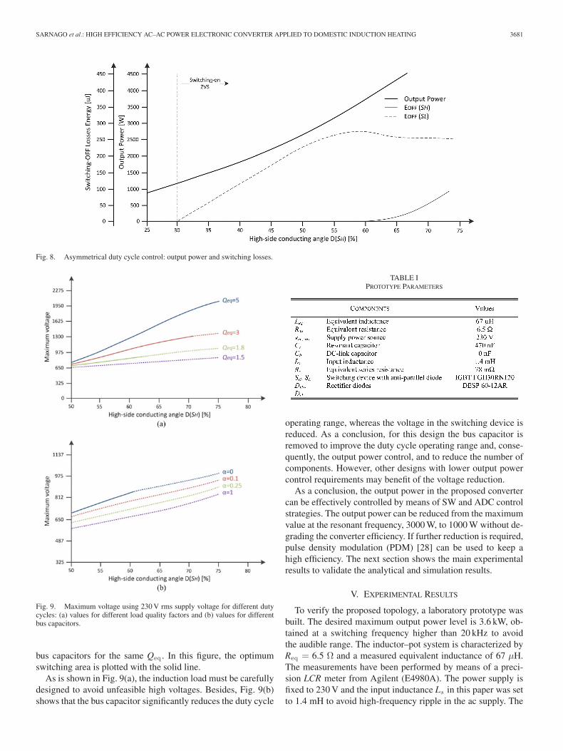
where θDT is the dead-time conducting angle to avoid shortcircuits. The variation of conducting angle is restricted bythe achievement of soft-switching conditions for SH , ZVS forswitching-off, and by the achievement of ZVS in the switching-on commutation for both devices (antiparallel diode conductionat the beginning). In order to operate with switch-on ZVS con-ditions, the duty cycle must be higher than 30%. The upperboundary is kept to 60% to obtain a proper safety margin andbalance the total amount of losses per switching device. Fig. 8shows the power output variation achieved and the switchinglosses.
One of the key design aspects when designing the proposedconverter to operate with the ADC control is the voltage that theswitching devices must withstand. Fig. 9 shows the value of thevoltage normalized to the input mains voltage as a function ofthe duty cycle for loads with (a) different Qeq and (b) different
SARNAGO et al.: HIGH EFFICIENCY AC–AC POWER ELECTRONIC CONVERTER APPLIED TO DOMESTIC INDUCTION HEATING 3681
Fig. 8. Asymmetrical duty cycle control: output power and switching losses.
Fig. 9. Maximum voltage using 230 V rms supply voltage for different dutycycles: (a) values for different load quality factors and (b) values for differentbus capacitors.
bus capacitors for the same Qeq . In this figure, the optimumswitching area is plotted with the solid line.
As is shown in Fig. 9(a), the induction load must be carefullydesigned to avoid unfeasible high voltages. Besides, Fig. 9(b)shows that the bus capacitor significantly reduces the duty cycle
TABLE IPROTOTYPE PARAMETERS
operating range, whereas the voltage in the switching device isreduced. As a conclusion, for this design the bus capacitor isremoved to improve the duty cycle operating range and, conse-quently, the output power control, and to reduce the number ofcomponents. However, other designs with lower output powercontrol requirements may benefit of the voltage reduction.
As a conclusion, the output power in the proposed convertercan be effectively controlled by means of SW and ADC controlstrategies. The output power can be reduced from the maximumvalue at the resonant frequency, 3000 W, to 1000 W without de-grading the converter efficiency. If further reduction is required,pulse density modulation (PDM) [28] can be used to keep ahigh efficiency. The next section shows the main experimentalresults to validate the analytical and simulation results.
V. EXPERIMENTAL RESULTS
To verify the proposed topology, a laboratory prototype wasbuilt. The desired maximum output power level is 3.6 kW, ob-tained at a switching frequency higher than 20 kHz to avoidthe audible range. The inductor–pot system is characterized byReq = 6.5 Ω and a measured equivalent inductance of 67 μH.The measurements have been performed by means of a preci-sion LCR meter from Agilent (E4980A). The power supply isfixed to 230 V and the input inductance Ls in this paper was setto 1.4 mH to avoid high-frequency ripple in the ac supply. The
3682 IEEE TRANSACTIONS ON POWER ELECTRONICS, VOL. 27, NO. 8, AUGUST 2012
Fig. 10. Measured main waveforms. From top to bottom: inductor current(15 A/div), voltage (150 V/div), and current (15 A/div) in the high-side switch;and voltage (150 V/div) and current (15 A/div) in the low-side switch. Time:4 μs/div.
control signals are generated by means of an FPGA-based digitalpulsewidth modulator [29], [30]. Table I shows the componentvalues for the prototype.
The main waveforms during a switching period for a 50%duty cycle are shown in Fig. 10, including the inductor current,and voltage and current through the switching devices. Besides,Fig. 11 shows the input voltage and current, and the load cur-rent during a mains half-cycle period. These measurements havebeen performed with an input inductor Ls = 1.4 mH, consideredin the measured efficiency. If further input current ripple reduc-tion is required, either the power converter switching frequencyor the input inductance can be increased. As a conclusion, thesewaveforms match up with the theoretical expected ones, andverify the proper operation of the converter.
The efficiency of the power converter has been measured us-ing the power analyzer YOKOGAWA PZ-4000. The efficiencyexperimental results for both SW and ADC control strategiesare shown in Fig. 12, where a comparison with the classical
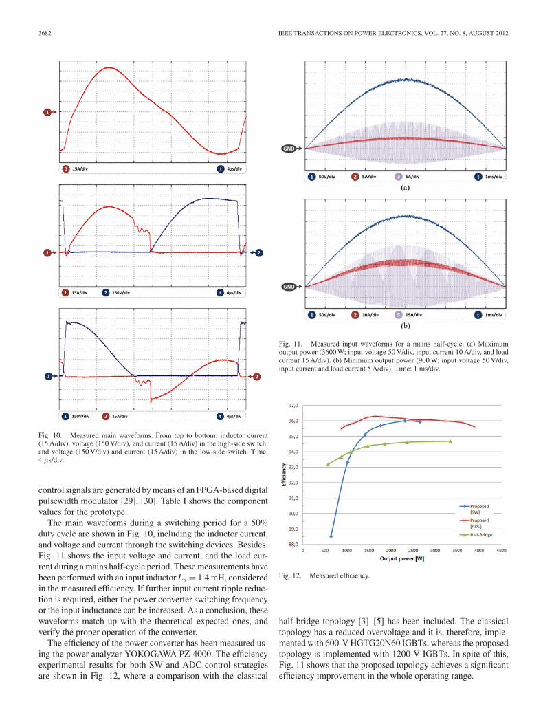
Fig. 11. Measured input waveforms for a mains half-cycle. (a) Maximumoutput power (3600 W; input voltage 50 V/div, input current 10 A/div, and loadcurrent 15 A/div). (b) Minimum output power (900 W; input voltage 50 V/div,input current and load current 5 A/div). Time: 1 ms/div.
Fig. 12. Measured efficiency.
half-bridge topology [3]–[5] has been included. The classicaltopology has a reduced overvoltage and it is, therefore, imple-mented with 600-V HGTG20N60 IGBTs, whereas the proposedtopology is implemented with 1200-V IGBTs. In spite of this,Fig. 11 shows that the proposed topology achieves a significantefficiency improvement in the whole operating range.

SARNAGO et al.: HIGH EFFICIENCY AC–AC POWER ELECTRONIC CONVERTER APPLIED TO DOMESTIC INDUCTION HEATING 3683
On one hand, the SW control strategy achieves a higher effi-ciency in the high-output power range. However, the efficiencysignificantly decreases in the low-output power range due to theswitching losses. On the other hand, the ADC control achievesthe same high efficiency in the high-output power range, butit remains constant due to the soft-switching conditions. It isimportant to note that the proposed topology with ADC controlachieves a significant efficiency improvement compared withthe classical half-bridge topology due to the power devices andcurrent reduction and the soft-switching conditions.
VI. CONCLUSION
This paper presents a new ac–ac converter applied to domes-tic induction heating. An analytical analysis has been performedin order to obtain the equations and operation modes that de-scribe the proposed converter. The converter can operate withzero-voltage switching during both turn-on and turn-off commu-tations. Besides, the output voltage is doubled compared to theclassical half-bridge, reducing the current through the switch-ing devices. As a consequence, the power converter efficiencyis improved in the whole operating range.
A 3.6-kW prototype has been designed and implementedin order to validate the analytical and simulation results. Theexperimental measurements show a significant efficiency im-provement compared to the classical half-bridge topology andvalidate the feasibility of the proposed converter.
REFERENCES
[1] J. Acero, J. M. Burdio, L. A. Barragan, D. Navarro, R. Alonso, J. R. Garcia,F. Monterde, P. Hernandez, S. Llorente, and I. Garde, “Domestic inductionappliances,” IEEE Ind. Appl. Mag., vol. 16, no. 2, pp. 39–47, Mar./Apr.2010.
[2] H. Fujita, N. Uchida, and K. Ozaki, “A new zone-control induction heat-ing system using multiple inverter units applicable under mutual mag-netic coupling conditions,” IEEE Trans. Power Electron., vol. 26, no. 7,pp. 2009–2017, Jul. 2010.
[3] I. Millan, J. M. Burdıo, J. Acero, O. Lucıa, and S. Llorente, “Seriesresonant inverter with selective harmonic operation applied to all-metaldomestic induction heating,” IET Power Electron., vol. 4, pp. 587–592,May 2011.
[4] R. L. Steigerwald, “A comparison of half-bridge resonant convertertopologies,” IEEE Trans. Power Electron., vol. 3, no. 2, pp. 174–182,Apr. 1988.
[5] H. W. Koertzen, J. D. van Wyk, and J. A. Ferreira, “Design of the half-bridge series resonant converters for induction cooking,” in Proc. IEEEPower Electron. Spec. Conf. Records, 1995, pp. 729–735.
[6] H. Pham, H. Fujita, K. Ozaki, and N. Uchida, “Phase angle control ofhigh-frequency resonant currents in a multiple inverter system for zone-control induction heating,” IEEE Trans. Power Electron., vol. 26, no. 11,pp. 3357–3366, Nov. 2011.
[7] W. Yunxiang, M. A. Shafi, A. M. Knight, and R. A. McMahon, “Com-parison of the effects of continuous and discontinuous PWM schemeson power losses of voltage-sourced inverters for induction motor drives,”IEEE Trans. Power Electron., vol. 26, no. 1, pp. 182–191, Jan. 2011.
[8] I. Takahashi, “Power factor improvement of a diode rectifier circuit bydither signals,” in Conf. Record IEEE Ind. Appl. Soc. Annu. Meet., 1990,pp. 1289–1294.
[9] A. A. Boora, A. Nami, F. Zare, A. Ghosh, and F. Blaabjerg, “Voltage-sharing converter to supply single-phase asymmetrical four-level diode-clamped inverter with high power factor loads,” IEEE Trans. PowerElectron., vol. 25, no. 10, pp. 2507–2520, Oct. 2010.
[10] L. Meng, K. Cheng, and K. Chan, “Systematic approach to high-powerand energy-efficient industrial induction cooker system: Circuit design,control strategy and prototype evaluation,” IEEE Trans. Power Electron.,vol. 26, no. 12, pp. 3754–3765, Dec. 2011.
[11] N. Nguyen-Quang, D. A. Stone, C. M. Bingham, and M. P. Foster, “Singlephase matrix converter for radio frequency induction heating,” in Proc.IEEE Int. Symp. Power Electron., Electr. Drives, Autom. Motion, May,2006, pp. 614–618.
[12] N. Nguyen-Quang, D. A. Stone, C. Bingham, and M. P. Foster, “Com-parison of single-phase matrix converter and H-bridge converter for radiofrequency induction heating,” in Proc. Eur. Conf. Power Electron. Appl.,2007, pp. 1–9.
[13] O. Lucıa, F. Almazan, J. Acero, J. M. Burdıo, and C. Carretero, “Multiple-output resonant matrix converter for multiple-inductive-load systems,” inProc. IEEE Appl. Power Electron. Conf. Expo., 2011, pp. 1338–1343.
[14] L. Gang, S. Kai, H. Lipei, and I. Seiki, “RB-IGBT gate drive circuit andits application in two-stage matrix converter,” in Proc. IEEE Appl. PowerElectron. Conf. Expo., 2008, pp. 245–251.
[15] H. Sugimura, S.-P. Mun, S.-K. Kwon, T. Mishima, and M. Nakaoka,“High-frequency resonant matrix converter using one-chip reverse block-ing IGBT-based bidirectional switches for induction heating,” in Proc.IEEE Power Electron. Spec. Conf., 2008, pp. 3960–3966.
[16] C. Aguilar, A. Ruiz, F. Canales, and F. Lee, “Analysis of the half-bridgeboost rectifier as integrated electronic ballast with power factor correc-tion,” in Proc. IEEE Power Electron. Spec. Conf., 2001, pp. 707–712.
[17] N. A. Ahmed and M. Nakaoka, “Boost-half-bridge edge resonant softswitching PWM high-frequency inverter for consumer induction heatingappliances,” IEE Proc. Electr. Power Appl., vol. 153, no. 6, pp. 932–938,Nov. 2006.
[18] H. L. Cheng, C. S. Moo, and W. M. Chen, “A novel single-stage high-power-factor electronic ballast with symmetrical topology,” IEEE Trans.Ind. Electron., vol. 50, no. 4, pp. 759–766, Aug. 2003.
[19] W. Chien-Ming, “A novel single-stage high-power-factor electronic bal-last with symmetrical half-bridge topology,” IEEE Trans. Ind. Electron.,vol. 55, no. 2, pp. 969–972, Feb. 2008.
[20] R. N. do Prado, M. F. da Silva, M. Jungbeck, and A. R. Seidel, “Lowcost high-power-factor electronic ballast for compact fluorescent lamps,”in Proc. IEEE Ind. Appl. Conf., 1999, pp. 256–261.
[21] A. Ruiz, C. Aguilar, and J. Arau, “Half-bridge boost rectifier as powerfactor corrector-electronic balast [balast read ballast],” in IEEE PowerElectron. Congr., 2000, pp. 136–141.
[22] K. Chong-Eun, M. Gun-Woo, and H. Sang-Kyoo, “Voltage doubler recti-fied boost-integrated half bridge (VDRBHB) converter for digital car audioamplifiers,” IEEE Trans. Power Electron., vol. 22, no. 6, pp. 2321–2330,Nov. 2007.
[23] A. Fujita, H. Sadakata, I. Hirota, H. Omori, and M. Nakaoka, “Latestdevelopments of high-frequency series load resonant inverter type built-incooktops for induction heated all metallic appliances,” in IEEE PowerElectron. Motion Control Conf., 2009, pp. 2537–2544.
[24] J. Acero, C. Carretero, I. Millan, O. Lucıa, R. Alonso, and J. M. Burdıo,“Analysis and modeling of planar concentric windings forming adaptable-diameter burners for induction heating appliances,” IEEE Trans. PowerElectron., vol. 26, no. 5, pp. 1546–1558, May 2011.
[25] O. Lucıa, J. M. Burdıo, I. Millan, J. Acero, and L. A. Barragan, “Efficiencyoriented design of ZVS half-bridge series resonant inverter with variablefrequency duty cycle control,” IEEE Trans. Power Electron., vol. 25,no. 7, pp. 1671–1674, Jul. 2010.
[26] O. Lucıa, C. Carretero, D. Palacios, D. Valeau, and J. M. Burdıo, “Config-urable snubber network for efficiency optimization of resonant convertersapplied to multi-load induction heating,” Electron. Lett., vol. 47, no. 17,pp. 989–991, Aug. 2011.
[27] J. Kim, H. S. Song, and K. Nam, “Asymmetric duty control of a dual-half-bridge dc/dc converter for single-phase distributed generators,” IEEETrans. Power Electron., vol. 26, no. 3, pp. 973–982, May 2011.
[28] O. Lucıa, J. M. Burdıo, I. Millan, J. Acero, and D. Puyal, “Load-adaptivecontrol algorithm of half-bridge series resonant inverter for domestic in-duction heating,” IEEE Trans. Ind. Electron., vol. 56, no. 8, pp. 3106–3116, Aug. 2009.
[29] D. Navarro, O. Lucıa, L. A. Barragan, J. I. Artigas, and O. Jimenez,“Synchronous FPGA-based implementations of digital pulse width mod-ulators,” IEEE Trans. Power Electron., vol. 27, no. 5, pp. 2515–2525,May 2012.
[30] O. Lucıa, L. A. Barragan, J. M. Burdıo, O. Jimenez, D. Navarro, andI. Urriza, “A versatile power electronics test-bench architecture applied todomestic induction heating,” IEEE Trans. Ind. Electron., vol. 58, no. 3,pp. 998–1007, Mar. 2011.

3684 IEEE TRANSACTIONS ON POWER ELECTRONICS, VOL. 27, NO. 8, AUGUST 2012
Hector Sarnago (M’09) received the M.Sc. de-gree in electrical engineering from the University ofZaragoza, Zaragoza, Spain, in 2010, where he is cur-rently working toward the Ph.D. degree.
His main research interests include resonant con-verters and digital control for induction heatingapplications.
Mr. Sarnago is a member of the Aragon Institutefor Engineering Research (I3A).
Arturo Mediano (SM’06) received the M.Sc. andPh.D. degrees in electrical engineering from the Uni-versity of Zaragoza, Zaragoza, Spain, in 1990 and1997, respectively.
Since 1992 he has been involved in a teach-ing professorship with special interests in RF(HF/VHF/UHF) and EMI/EMC design for Telecomand Electrical Engineers. Since 1990, he has beeninvolved in design and management responsibilitiesfor research and development projects in the RF fieldfor communications, industry, and scientific applica-
tions. His research interest includes high-efficiency switching-mode RF poweramplifiers where he has experience in applications such as broadcast, mobilecommunication radios, through-earth communication systems, induction heat-ing, plasmas for industrial applications, and RF identification. He has an expe-rience in collaboration with industry (including training and consultancy in RFand electromagnetic interference/electromagnetic compatibility).
Dr. Mediano is an active member from 1999, now ViceChair, of the MTT-17 (HF/VHF/UHF technology) Technical Committee of the Microwave Theoryand Techniques Society of the IEEE.
Oscar Lucıa (S’04–M’11) received the M.Sc. andPh.D. degrees in electrical engineering from the Uni-versity of Zaragoza, Zaragoza, Spain, in 2006 and2010, respectively.
He is currently an Assistant Professor in the De-partment of Electronic Engineering and Communi-cations, University of Zaragoza. His main researchinterests include multiple output converters, digitalcontrol, and resonant power conversion for inductionheating applications.
Dr. Lucıa is a member of the Aragon Institute forEngineering Research (I3A).