3920 ieee transactions on antennas and …users.ece.gatech.edu/etentze/tap_2005_cp_uniformtw.pdf ·...
TRANSCRIPT

3920 IEEE TRANSACTIONS ON ANTENNAS AND PROPAGATION, VOL. 53, NO. 12, DECEMBER 2005
Determination of Reactance Loading for CircularlyPolarized Circular Loop Antennas With a Uniform
Traveling-Wave Current DistributionRongLin Li, Senior Member, IEEE, Nathan A. Bushyager, Member, IEEE, Joy Laskar, Fellow, IEEE, and
Manos M. Tentzeris, Senior Member, IEEE
Abstract—A simple theory is presented to predict the lumpedreactance loading for circularly polarized circular loop antennaswith a uniform traveling-wave current distribution. The reactiveload is located on a circular wire loop of one-wavelength circum-ference at a position of 45 away from the feed point. To achieve auniform traveling-wave current distribution, the loading reactanceand the input impedances of the loaded and unloaded loop an-tennas need to satisfy certain conditions. First, the input resistanceand the input reactance of the unloaded loop antenna should havethe same absolute value. Second, the input impedance of the loadedloop must be purely resistive and its value needs to be two times ofthe input resistance of the unloaded loop. Third, the loading re-actance should be chosen to be two times in value and oppositein sense of the input reactance of the unloaded loop. These con-ditions can be approximately met when the circular loop is placedabove a ground plane. The loading reactance is determined fromthe input impedance of the unloaded loop and is optimized foran optimal performance of circular polarization. It is found thatthe reactive load must be capacitive and its value depends on theheight of the loop above the ground plane and the thickness of thewire. The characteristics of the circular polarization and the inputimpedance of the capacitance-loaded circular loop antennas are in-vestigated. An experimental example is presented to verify the the-oretical prediction.
Index Terms—Circular loop antenna, circular polarization, re-actively loaded antenna, uniform traveling-wave current distribu-tion.
I. INTRODUCTION
I T IS well-known that a single-fed circular wire loop antennaof one-wavelength circumference (called one-wavelength
loop in short) creates a standing-wave current distribution andthus radiates a linearly polarized wave in the far-field zone[1]–[3]. It is also easy to understand that a one-wavelengthcircular loop can radiate perfectly circularly polarized wavesin the direction perpendicular to the plane of the loop if auniform traveling-wave current distribution is generated [4].A common way to produce a uniform traveling-wave currentdistribution is to feed the loop antenna with two 90 phase shiftedgenerators which are located 90 (or a quarter-wavelength) apartalong the loop so that a superposition of two standing-wave
Manuscript received November 1, 2004; revised April 30, 2005. This paperwas supported in part by NSF CAREER Award ECS-9984761 and in part byNSF Grant ECS-0 313 951.
The authors are with the Georgia Electronic Design Center, School of Elec-trical and Computer Engineering, Georgia Institute of Technology, Atlanta, GA30332-0250 USA (e-mail: [email protected]).
Digital Object Identifier 10.1109/TAP.2005.859767
current distributions with equal amplitude, 90 phase shift intime, and a quarter-wavelength difference in space results in aperfectly uniform traveling-wave current distribution [5]. Thedisadvantage of this approach is the need for two sources ora 90 hybrid coupler. Another commonly used technique forachieving a traveling-wave current distribution is to load theantenna with resistors [6]. Obviously the main problem of thismethod is that it leads to low antenna efficiency since theresistors absorb the majority of fed power. In the 1980s, it wasdemonstrated that a traveling-wave current distribution couldbe obtained if a circular loop is reactively loaded at a positionof 45 away from the feed point [7]. However, it was shown in[7] that the obtained traveling-wave current distributions werefar from uniform due to the high-value ( ohms) of theused reactance. (High-value impedance loading usually tends toblock the flowing of current, thus causing a dip in the magnitudeof the current distribution.) In addition, the loaded loop antennausually needs to be placed at a considerable height above aground plane (e.g., at a height of more than a quarter-wavelengthconsidered in [7]) and results in a high input impedance (e.g.,input resistance ohms and input reactance ohms),thus causing difficulties in matching the antenna to the feedingsystem. Most importantly, no theoretical prediction has beengiven in [7] for the value of the loading reactance; therefore itwas not clear why a traveling-wave current distribution couldbe achieved by the reactive load.
It is our purpose here to demonstrate that it is possible totheoretically predict the loading reactance for the launchingof a uniform traveling-wave current distribution along a one-wavelength circular loop antenna. It will be proven that thereare simple relationships among the loading reactance and theinput impedances of the loaded and unloaded loop antennas.Also, it will be found that the uniform traveling-wave currentdistribution can be created when a one-wavelength circular loopis situated at a height of much less than a quarter-wavelength(about 0.05–0.15 wavelengths considered in this paper) abovethe ground plane. Thus, the low-profile circular loop antennacan be loaded with a low-value capacitive reactance, leadingto smaller input impedance which facilitates the matching ofthe antenna.
This paper is organized as follows. First, the conditions fora uniform traveling-wave current distribution will be derived.Then, the uniform traveling-wave current distribution will be re-alized by placing a circular wire loop over a ground plane. The
0018-926X/$20.00 © 2005 IEEE

LI et al.: DETERMINATION OF REACTANCE LOADING FOR CIRCULAR LOOP ANTENNAS 3921
Fig. 1. Geometry of a circular loop antenna loaded at � = �=4 withimpedance Z .
characteristics of input impedance and circular polarization willbe investigated. Finally, a comparison of simulated and mea-sured results will be performed.
II. CONDITIONS FOR A UNIFORM TRAVELING-WAVE CURRENT
DISTRIBUTION
Consider a lossless circular wire loop antenna (shown inFig. 1) with a loop radius of and a wire radius of . It isassumed that the circumference of the loop is one wavelength
, i.e., , and that the wire radiussatisfies the “thin wire” approximation, i.e., [8]. Theloop is fed by a voltage source at and is loaded bya lumped impedance at . Under the “thin wire”approximation, the current distribution on the loop can be rep-resented by a filamentary current along theloop circumferential axis. We assume a uniform traveling-wavecurrent distribution created on the loop such that [9], [10]
(1)
where the plus sign (the upper part of the symbol “ ”) is usedfor a left-hand (with thumb in the direction) traveling-wavecurrent distribution and the minus sign (the lower part of thesymbol “ ”) is used for a right-hand traveling-wave current dis-tribution. Applying the compensation theorem, we can replacethe load with an equivalent loading voltage [11], [12]
(2)
According to the principle of superposition [13], the currentdistribution can be obtained by the superposition of the twocurrents in the loop when fed by each voltage source alone, thatis
(3)
where and are generated by the feeding voltageat and the loading voltage at , respectively,
Fig. 2. Current distribution on a loaded circular loop antenna is equal to asuperposition of the currents generated by the feeding voltageV and the loadingvoltage V .
as illustrated in Fig. 2. It is a reasonable approximation to repre-sent these current distributions on a single-fed one-wavelengthcircular loop with a cosinusoidal variation [12], [14]
(4a)
(4b)
With the input impedance of the circular loop antenna withoutthe load, (simply called “unloaded input impedance”), thecurrent constants and are given by
(5a)
(5b)
[Note that from (2)]. Substituting (4) in(3) with and from (5) leads to
(6)
Substituting into the left side of (6) and re-placing with , where is the input impedanceof the circular loop antenna with the load (simply called “loadedinput impedance”) we obtain
(7)
Dividing on both sides of (7) by and moving to theleft side and to the right side, we obtain the solution forthe loading impedance:
(8)
After a simple algebra manipulation, (8) becomes
(9)
Since (fixed at ) is independent of , we musthave
(10)
Therefore we obtain the precondition for a uniform traveling-wave current distribution specified on the one-wavelength cir-cular loop, that is
(11)

3922 IEEE TRANSACTIONS ON ANTENNAS AND PROPAGATION, VOL. 53, NO. 12, DECEMBER 2005
This means that in order to realize a uniform traveling-wavecurrent distribution, the loaded and unloaded input impedancesof the circular loop antenna must be subject to a certain relation-ship given by (11). As a consequence of the precondition (11),we can find by substituting (10) in (9) the value of the loadingimpedance
(12)
which is also considered as the implementation condition for theuniform traveling-wave current distribution.
Now let us check whether a uniform traveling-wave currentdistribution can be really achieved if the precondition (11)and the implementation condition (12) are satisfied. Substi-tuting (11) for and (12) for in (6) and considering
, we obtain
(13)
The above equation can be further simplified as
(14)
which indeed confirms a uniform traveling-wave current distri-bution.
For a purely reactive load, can be expressed as
(15a)
(15b)
where is a positive real number. Substituting (15) in the leftside of (12) gives
(16a)
(16b)
To guarantee the right side of (16) being equal to a positivenumber, we have the following observations:
1) For an inductive load, the input resistance and the inputreactance of the unloaded circular loop antenna musthave the same absolute value but with an opposite sign,that is
(17)
2) There only exists a right-hand traveling-wave currentdistribution for the inductive load since we have tochoose the lower part of the symbol “ ” in (16a).
3) For a capacitive load, the input resistance and inputreactance of the unloaded circular loop antenna musthave the same value, that is
(18)
Fig. 3. Current distribution on an isolated circular loop antenna loaded byan inductance with Z = j194 ohms at � = �=4 [V = 1 volt, =2 ln(2�b=a) = 10], showing a bad traveling-wave current distribution.
4) There only exists a left-hand traveling-wave currentdistribution for the capacitive load since we have tochoose the upper part of the symbol “ ” in (16b).
5) The value of the loading reactance should be equal tothe summation of the absolute values of the unloadedinput resistance and input reactance or simply equal totwo times of the unloaded input resistance since theunloaded input resistance and reactance have the sameabsolute value, i.e., .
6) The input impedance of the loaded circular loop an-tenna must be a real number and its value has to beequal to the value of the loading reactance, namely,
.
It should be noted that loading a one-wavelength circular loopantenna with does not automatically resultin a uniform traveling-wave current distribution even though theunloaded input impedance meets as required byObservations 1) and 3). Whether a uniform traveling-wave cur-rent distribution can be really realized also depends on the loadedinput impedance, i.e., the precondition (11). As an example, let usconsider an isolated circular loop antenna in air. For a one-wave-length circular loop with , it is easy to findby numerical simulation (e.g., the method of moment, MoM) orfrom references (e.g., [15]) that the unloaded input impedanceis about ohms (obtained here using NEC1.1), approximately satisfying the condition foran inductive load, i.e., satisfying Observation 1). Now we loadthe loop with a lumped inductance with ohms (i.e.,
) at and obtain the current distribu-tion along the loop, as shown in Fig. 3. We can see that the cur-rent distribution indeed presents some right-hand traveling-wavefeatures but it differs significantly from a satisfactory uniformtraveling-wave current. The reason for this current distributionis the high imaginary part of the current at the feed point, whichleads to a considerable reactive component in the loaded inputimpedance. In fact it is found that the loaded input impedance isapproximately equal to ohms, which by nomeans is a purely real impedance as noted at Observation 6). In
LI et al.: DETERMINATION OF REACTANCE LOADING FOR CIRCULAR LOOP ANTENNAS 3923
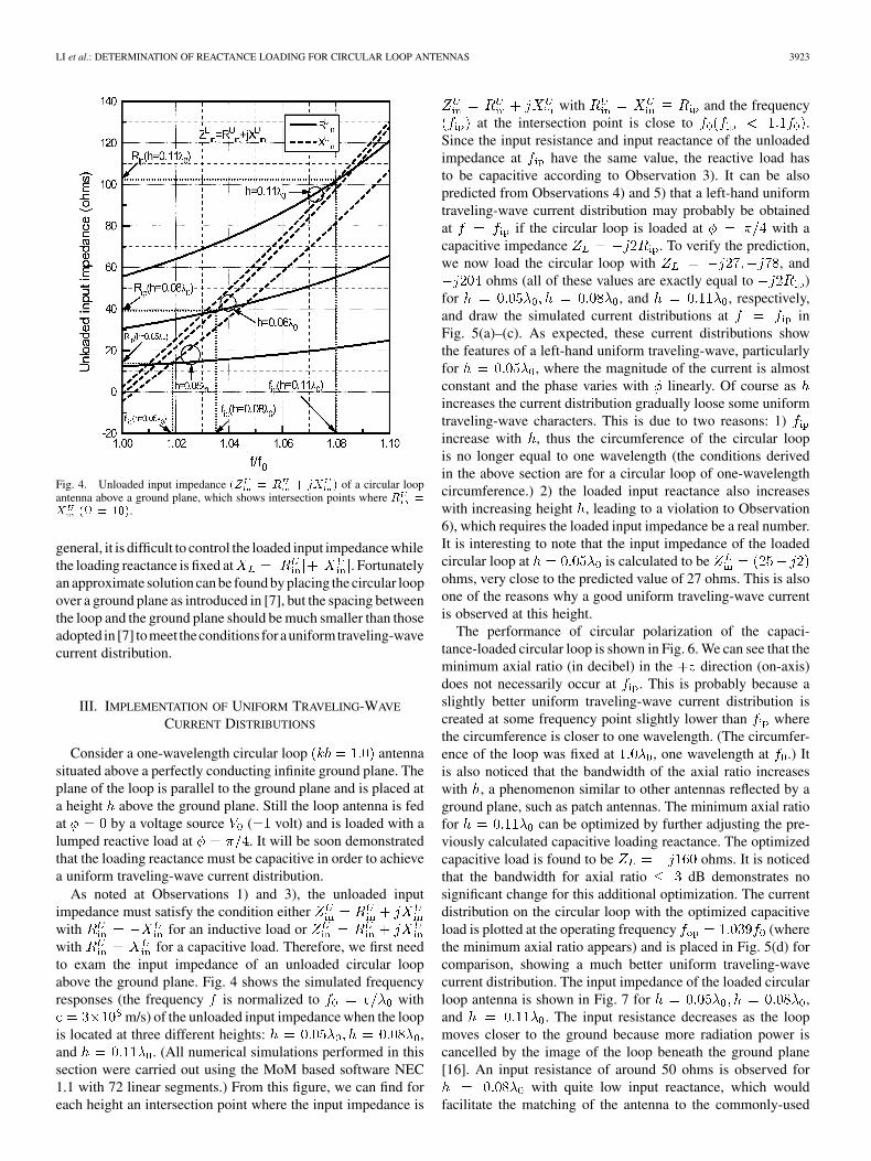
Fig. 4. Unloaded input impedance (Z = R + jX ) of a circular loopantenna above a ground plane, which shows intersection points where R =X ( = 10).
general, it is difficult to control the loaded input impedance whilethe loading reactance is fixed at . Fortunatelyan approximate solution can be found by placing the circular loopover a ground plane as introduced in [7], but the spacing betweenthe loop and the ground plane should be much smaller than thoseadopted in [7] tomeet theconditions forauniformtraveling-wavecurrent distribution.
III. IMPLEMENTATION OF UNIFORM TRAVELING-WAVE
CURRENT DISTRIBUTIONS
Consider a one-wavelength circular loop antennasituated above a perfectly conducting infinite ground plane. Theplane of the loop is parallel to the ground plane and is placed ata height above the ground plane. Still the loop antenna is fedat by a voltage source ( volt) and is loaded with alumped reactive load at . It will be soon demonstratedthat the loading reactance must be capacitive in order to achievea uniform traveling-wave current distribution.
As noted at Observations 1) and 3), the unloaded inputimpedance must satisfy the condition eitherwith for an inductive load orwith for a capacitive load. Therefore, we first needto exam the input impedance of an unloaded circular loopabove the ground plane. Fig. 4 shows the simulated frequencyresponses (the frequency is normalized to with
m/s) of the unloaded input impedance when the loopis located at three different heights: ,and . (All numerical simulations performed in thissection were carried out using the MoM based software NEC1.1 with 72 linear segments.) From this figure, we can find foreach height an intersection point where the input impedance is
with and the frequencyat the intersection point is close to .
Since the input resistance and input reactance of the unloadedimpedance at have the same value, the reactive load hasto be capacitive according to Observation 3). It can be alsopredicted from Observations 4) and 5) that a left-hand uniformtraveling-wave current distribution may probably be obtainedat if the circular loop is loaded at with acapacitive impedance . To verify the prediction,we now load the circular loop with , and
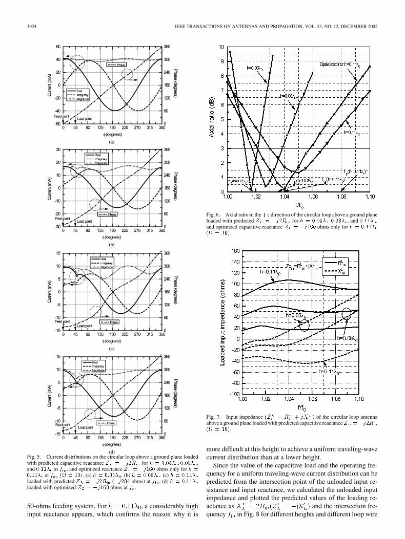
ohms (all of these values are exactly equal to )for , and , respectively,and draw the simulated current distributions at inFig. 5(a)–(c). As expected, these current distributions showthe features of a left-hand uniform traveling-wave, particularlyfor , where the magnitude of the current is almostconstant and the phase varies with linearly. Of course asincreases the current distribution gradually loose some uniformtraveling-wave characters. This is due to two reasons: 1)increase with , thus the circumference of the circular loopis no longer equal to one wavelength (the conditions derivedin the above section are for a circular loop of one-wavelengthcircumference.) 2) the loaded input reactance also increaseswith increasing height , leading to a violation to Observation6), which requires the loaded input impedance be a real number.It is interesting to note that the input impedance of the loadedcircular loop at is calculated to beohms, very close to the predicted value of 27 ohms. This is alsoone of the reasons why a good uniform traveling-wave currentis observed at this height.
The performance of circular polarization of the capaci-tance-loaded circular loop is shown in Fig. 6. We can see that theminimum axial ratio (in decibel) in the direction (on-axis)does not necessarily occur at . This is probably because aslightly better uniform traveling-wave current distribution iscreated at some frequency point slightly lower than wherethe circumference is closer to one wavelength. (The circumfer-ence of the loop was fixed at , one wavelength at .) Itis also noticed that the bandwidth of the axial ratio increaseswith , a phenomenon similar to other antennas reflected by aground plane, such as patch antennas. The minimum axial ratiofor can be optimized by further adjusting the pre-viously calculated capacitive loading reactance. The optimizedcapacitive load is found to be ohms. It is noticedthat the bandwidth for axial ratio dB demonstrates nosignificant change for this additional optimization. The currentdistribution on the circular loop with the optimized capacitiveload is plotted at the operating frequency (wherethe minimum axial ratio appears) and is placed in Fig. 5(d) forcomparison, showing a much better uniform traveling-wavecurrent distribution. The input impedance of the loaded circularloop antenna is shown in Fig. 7 for ,and . The input resistance decreases as the loopmoves closer to the ground because more radiation power iscancelled by the image of the loop beneath the ground plane[16]. An input resistance of around 50 ohms is observed for
with quite low input reactance, which wouldfacilitate the matching of the antenna to the commonly-used
3924 IEEE TRANSACTIONS ON ANTENNAS AND PROPAGATION, VOL. 53, NO. 12, DECEMBER 2005
Fig. 5. Current distributions on the circular loop above a ground plane loadedwith predicted capacitive reactance Z = �j2R for h = 0:05� ; 0:08� ,and 0:11� at f , and optimized reactance Z = �j160 ohms only for h =0:11� at f ( = 10). (a) h = 0:05� . (b) h = 0:08� . (c) h = 0:11�loaded with predicted Z = �j2R (�j204 ohms) at f . (d) h = 0:11�loaded with optimized Z = �j160 ohms at f .
50-ohms feeding system. For , a considerably highinput reactance appears, which confirms the reason why it is
Fig. 6. Axial ratio in the+z direction of the circular loop above a ground planeloaded with predicted Z = �j2R for h = 0:05� ; 0:08� , and 0:11� ,and optimized capacitive reactance Z = �j160 ohms only for h = 0:11�( = 10).
Fig. 7. Input impedance (Z = R + jX ) of the circular loop antennaabove a ground plane loaded with predicted capacitive reactanceZ = �j2R( = 10).
more difficult at this height to achieve a uniform traveling-wavecurrent distribution than at a lower height.
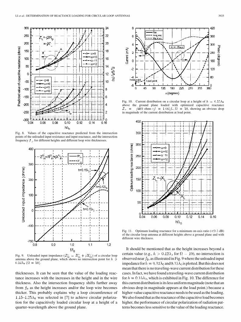
Since the value of the capacitive load and the operating fre-quency for a uniform traveling-wave current distribution can bepredicted from the intersection point of the unloaded input re-sistance and input reactance, we calculated the unloaded inputimpedance and plotted the predicted values of the loading re-actance as and the intersection fre-quency in Fig. 8 for different heights and different loop wire
LI et al.: DETERMINATION OF REACTANCE LOADING FOR CIRCULAR LOOP ANTENNAS 3925
Fig. 8. Values of the capacitive reactance predicted from the intersectionpoints of the unloaded input resistance and input reactance, and the intersectionfrequency f for different heights and different loop wire thicknesses.
Fig. 9. Unloaded input impedance (Z = R + jX ) of a circular loopantenna above the ground plane, which shows no intersection point for h0:12� ( = 10).
thicknesses. It can be seen that the value of the loading reac-tance increases with the increases in the height and in the wirethickness. Also the intersection frequency shifts further awayfrom as the height increases and/or the loop wire becomesthicker. This probably explains why a loop circumference of
– was selected in [7] to achieve circular polariza-tion for the capacitively loaded circular loop at a height of aquarter-wavelength above the ground plane.
Fig. 10. Current distribution on a circular loop at a height of h = 0:15�above the ground plane loaded with optimized capacitive reactanceZ = �j400 ohms (f = 1:06)f ; = 10, showing an obvious dropin magnitude of the current distribution at load point.
Fig. 11. Optimum loading reactance for a minimum on-axis ratio (<0:5 dB)of the circular loop antenna at different heights above a ground plane and withdifferent wire thickness.
It should be mentioned that as the height increases beyond acertain value (e.g., for ), no intersection isobserved near , as illustrated in Fig. 9 where the unloaded inputimpedancefor and isplotted.But thisdoesnotmean that there is no traveling-wave current distribution for thesecases. In fact,we have found a traveling-wave currentdistributionfor , which is exhibited in Fig. 10. The difference forthis currentdistribution is its less uniform magnitude (note that anobvious drop in magnitude appears at the load point.) because ahigher-value capacitive reactance needs to be used as the loading.Wealso found thatas the reactanceof thecapacitive loadbecomeshigher, the performance of circular polarization of radiation pat-terns becomes less sensitive to the value of the loading reactance.

3926 IEEE TRANSACTIONS ON ANTENNAS AND PROPAGATION, VOL. 53, NO. 12, DECEMBER 2005
Fig. 12. Operating frequency at which the minimum on-axis axial ratioappears for the capacitance-loaded circular loop antenna at different heightsabove a ground plane and with different wire thickness.
Fig. 13. Bandwidth of on-axis axial ratio (�3 dB) of the capacitance-loadedcircular loop antenna as a function of the loop height and wire thickness.
Fig. 14. Input impedance (Z = R + jX ) of the capacitance-loadedcircular loop antenna with different loop heights and wire thicknesses.
For example, the on-axis axial ratio ( and )can remain below 1 dB even though the loading reactance varies
Fig. 15. Radiation patterns of the capacitance-loaded circular loop antennaon cuts � = 0 ; 45 ; 90 , and 135 for h = 0:05� , and h = 0:1� , andh = 0:15� ( = 10). (a) h = 0:05� . (b) h = 0:1� . (c) h = 0:15� .
from 350 ohms to 550 ohms. In effect, for a high-value capaci-tive reactance, it is possible to introduce a gap on the loop for areplacement of the capacitive loading and the desirable perfor-mance of circular polarization can be achieved by adjusting thewidth of the gap [17].
On the basis of theoretical prediction, we optimized the ca-pacitive loading for a minimum on-axis axial ratio ( dB) ofthe circular loop antenna at different heights –above the ground plane and with different wire thickness
. The optimum loading reactance is plotted in Fig. 11.Comparing with Fig. 8, we find that the optimum reactance isvery close to the predicted values for and .The operating frequency at which the minimum on-axisaxial ratio appears is shown in Fig. 12. We can see that the fre-quency shift increases with the increases in the loop height andin the wire thickness, but the maximum frequency shift is less
LI et al.: DETERMINATION OF REACTANCE LOADING FOR CIRCULAR LOOP ANTENNAS 3927
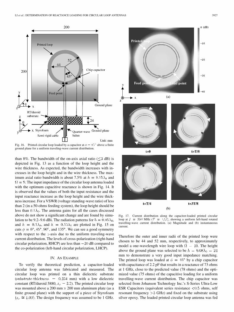
Fig. 16. Printed circular loop loaded by a capacitor at � = 45 above a finiteground plane for a uniform traveling-wave current distribution.
than 8%. The bandwidth of the on-axis axial ratio ( dB) isdepicted in Fig. 13 as a function of the loop height and thewire thickness. As expected, the bandwidth increases with in-creases in the loop height and in the wire thickness. The max-imum axial ratio bandwidth is about 7.5% at and
. The input impedance of the circular loop antenna loadedwith the optimum capacitive reactance is shown in Fig. 14. Itis observed that the values of both the input resistance and theinput reactance increase as the loop height and the wire thick-ness increase. For a VSWR (voltage standing-wave ratio) of lessthan 2 (in a 50-ohms feeding system), the loop height should beless than . The antenna gains for all the cases discussedabove do not show a significant change and are found by simu-lation to be 9.2–9.6 dBi. The radiation patterns for ,and , and are plotted in Fig. 15 oncuts , and 135 . We can see a good symmetrywith respect to the -axis due to the uniform traveling-wavecurrent distribution. The levels of cross-polarization (right-handcircular polarization, RHCP) are less than dB compared tothe co-polarization (left-hand circular polarization, LHCP).
IV. AN EXAMPLE
To verify the theoretical prediction, a capacitor-loadedcircular loop antenna was fabricated and measured. Thecircular loop was printed on a thin dielectric substrate( mm) with a low dielectricconstant (RT/duroid 5880, ). The printed circular loopwas mounted above a 200 mm 200 mm aluminum plate (as afinite ground plane) with the support of a piece of Styrofoam
. The design frequency was assumed to be 1 GHz.
Fig. 17. Current distribution along the capacitor-loaded printed circularloop at f = 994 MHz (T = 1=f), showing a uniform left-hand rotatedtravelling-wave current distribution. (a) Magnitude and (b) instantaneouscurrent.
Therefore the outer and inner radii of the printed loop werechosen to be 44 and 52 mm, respectively, to approximatelymodel a one-wavelength wire loop with . The heightabove the ground plane was selected to bemm to demonstrate a very good input impedance matching.The printed loop was loaded at by a chip capacitorwith capacitance of 2.2 pF that results in a reactance of 73 ohmsat 1 GHz, close to the predicted value (78 ohms) and the opti-mized value (75 ohms) of the capacitive loading for a uniformtravelling-wave current distribution. The chip capacitor wasselected from Johanson Technology Inc.’s S-Series Ultra-LowESR Capacitors (equivalent series resistance ohms, selfresonant frequency GHz) and fixed on the substrate usingsilver epoxy. The loaded printed circular loop antenna was fed
3928 IEEE TRANSACTIONS ON ANTENNAS AND PROPAGATION, VOL. 53, NO. 12, DECEMBER 2005
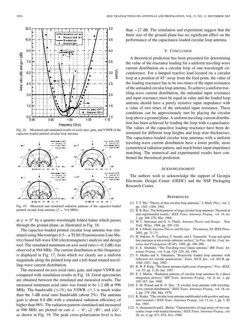
Fig. 18. Measured and simulated results of axial ratio, gain, and VSWR of thecapacitor-loaded printed circular loop antenna.
Fig. 19. Measured and simulated radiation patterns of the capacitor-loadedprinted circular loop antenna (f = 996 MHz).
at by a quarter-wavelength folded balun which passesthrough the ground plane, as illustrated in Fig. 16.
The capacitor-loaded printed circular loop antenna was sim-ulated using Microstripes 6.5—a TLM (Transmission-Line Ma-trix) based full-wave EM (electromagnetic) analysis and designtool. The simulated minimum on-axis axial ratio ( dB) wasobserved at 994 MHz. The current distribution at this frequencyis displayed in Fig. 17, from which we clearly see a uniformmagnitude along the printed loop and a left-hand rotated travel-ling-wave current distribution.
The measured on-axis axial ratio, gain, and input VSWR arecompared with simulation results in Fig. 18. Good agreementsare obtained between the simulated and measured results. Themeasured minimum axial ratio was found to be 1.2 dB at 996MHz. The bandwidth % for VSWR is much widerthan the 3-dB axial ratio bandwidth (about 2%). The antennagain is about 8.8 dBi with a simulated radiation efficiency ofhigher than 98%. The radiation patterns simulated and measuredat 996 MHz are plotted on cuts , and ,as shown in Fig. 19. The peak cross-polarization level is less
than dB. The simulation and experiment suggest that thefinite size of the ground plane has no significant effect on theperformance of the capacitance-loaded circular loop antenna.
V. CONCLUSION
A theoretical prediction has been presented for determiningthe value of the reactance loading for a uniform traveling-wavecurrent distribution on a circular loop of one-wavelength cir-cumference. For a lumped reactive load located on a circularloop at a position of 45 away from the feed point, the value ofthe loading reactance has to be two times of the input resistanceof the unloaded circular loop antenna. To achieve a uniform trav-eling-wave current distribution, the unloaded input resistanceand input reactance must be equal in value and the loaded loopantenna should have a purely resistive input impedance witha value of two times of the unloaded input resistance. Theseconditions can be approximately met by placing the circularloop above a ground plane. A uniform traveling-current distribu-tion has been achieved by loading the loop with a capacitance.The values of the capacitive loading reactance have been de-termined for different loop heights and loop wire thicknesses.The capacitance-loaded circular loop antennas with a uniformtraveling-wave current distribution have a lower profile, moresymmetrical radiation pattern, and much better input impedancematching. The numerical and experimental results have con-firmed the theoretical prediction.
ACKNOWLEDGMENT
The authors wish to acknowledge the support of GeorgiaElectronic Design Center (GEDC) and the NSF PackagingResearch Center.
REFERENCES
[1] T. T. Wu, “Theory of thin circular loop antennas,” J. Math. Phys., vol. 3,pp. 1301–1304, 1962.
[2] B. R. Rao, “Far field patterns of large circular loop antennas: Theoreticaland experimental results,” IEEE Trans. Antennas Propag., vol. 16, no.2, pp. 269–270, Mar. 1968.
[3] W. L. Stutzman and G. A. Thiele, Antenna Theory and Design. NewYork: Wiley, 1998, pp. 205–210.
[4] R. S. Elliott, Antenna Theory and Design. Piscataway, NJ: IEEE Press,2003, pp. 71–73.
[5] H. Nakano, N. Tsuchiya, T. Suzuki, and J. Yamauchi, “Loop and spiralline antennas at microstrip substrate surface,” in Proc. 6th Int. Conf. An-tenna and Propagation (ICAP), 1989, pp. 196–200.
[6] E. E. Altshuler, “The Traveling-wave linear antenna,” IRE Trans. An-tennas Propag., vol. 9, pp. 324–329, Jul. 1961.
[7] S. Okuba and S. Tokumaru, “Reactively loaded loop antennas withreflectors for circular polarization,” Trans. IECE Jpn., vol. J65-B, pp.1044–1051, Aug. 1982.
[8] R. W. P. King, “The linear antenna-eight years of progress,” Proc. IEEE,vol. 55, pp. 2–26, Jan. 1967.
[9] E. J. Martin, “Radiation patterns of circular loop antennas by a directintegration process,” IRE Trans. Antennas Propag., vol. 8, no. 1, pp.105–107, Jan. 1960.
[10] S. M. Prasad and B. N. Das, “A circular loop antenna with traveling-wave current distribution,” IEEE Trans. Antennas Propag., vol. 18, no.2, pp. 278–280, Mar. 1970.
[11] K. Iizuka, “The circular loop antenna multiloaded with positive and neg-ative resistors,” IEEE Trans. Antennas Propag., vol. 13, no. 1, pp. 7–20,Jan. 1965.
[12] A. shoamanesh and L. Shafai, “Characteristics of yagi arrays of two con-centric loops with loaded elements,” IEEE Trans. Antennas Propag., vol.28, no. 6, pp. 871–874, Nov. 1980.

LI et al.: DETERMINATION OF REACTANCE LOADING FOR CIRCULAR LOOP ANTENNAS 3929
[13] J.-L. Lin and K.-M. Chen, “Minimization of backscattering of a loopby impedance loading- theory and experiment,” IEEE Trans. AntennasPropag., vol. 16, no. 3, pp. 299–304, May 1968.
[14] J. E. Lindsay, “A circular loop antenna with nonuniform current distri-bution,” IRE Trans. Antennas Propag., vol. 8, pp. 439–441, Jul. 1960.
[15] J. E. Storver, “Impedance of thin-wire loop antennas,” AIEE Trans., vol.75, Nov. 1956.
[16] A. Shoamanesh and L. Shafai, “Characteristics of circular antenna abovea lossless ground plane,” IEEE Trans. Antennas Propag., vol. 29, no. 3,pp. 528–529, May 1981.
[17] H. Morishita, K. Hirasawa, and T. Nagao, “Circularly polarized wireantenna with a dual rhombic loop,” Proc. Inst. Elect. Eng. Microw. An-tennas Propag., pt. H, vol. 145, June 1998.
RongLin Li (M’02–SM’03) received the B.S. degreein electrical engineering from Xi’an Jiaotong Univer-sity, China, in 1983 and the M.S. and Ph.D. degreesin electrical engineering from Chongqing University,China, in 1990 and 1994, respectively.
From 1983 to 1987, he was an Electrical Engineerwith the Yunnan Electric Power Research Institute.From 1994 to 1996, he was a Postdoctoral ResearchFellow with Zhejiang University, China. In 1997, hewas with Hosei University, Japan, as a Hosei Interna-tional Fund Research Fellow. Since 1998, he has been
a Professor with Zhejiang University. In 1999, he was a Research Associate withthe University of Utah. In 2000, he was a Research Fellow with Queen’s Uni-versity of Belfast, U.K. In 2001, he joined the ATHENA group as a ResearchScientist with the Georgia Institute of Technology, Atlanta. His latest researchinterests include computational electromagnetics, modeling of antennas and mi-crowave devices, and RF packaging design.
Nathan A. Bushyager (S’99–M’05) received theB.S. degree in engineering science from The Penn-sylvania State University, State College, in 1999and the M.S. and Ph.D. degrees from The GeorgiaInstitute of Technology, Atlanta, in 2003 and 2004,respectively.
Currently, he is a Postdoctoral Fellow withthe Georgia Tech-NSF Microsystems PackagingResearch Center. He has authored a book, a bookchapter, six journal papers, and has presented morethan 30 conference papers. His research interests
include electromagnetic simulation and RF/microwave design and fabrication.His electromagnetic simulation work focuses on the wavelet based MRTDtechnique, statistical optimization methods, and hybrid simulators couplingmechanical and semiconductor physics with electromagnetics. In his designand fabrication work he develops multilayer RF components including filters,baluns, diplexers, phase shifters, and antennas in a variety of technologiesincluding semiconductors, ceramic, and organic substrates.
Dr. Bushyager was the recipient of the Best Student Paper Award at the 17thAnnual Review of Progress in Applied Computational Electromagnetics (ACESSociety) Conference in 2001.
Joy Laskar (S’84–M’85–SM’02–F’05) received theB.S. degree in computer engineering (math/physicsminors, highest honors) from Clemson University,Clemson, SC, in 1985 and the M.S. and Ph.D.degrees in electrical engineering from the Universityof Illinois, Urbana-Champaign, in 1989 and 1991,respectively.
Prior to joining the Georgia Institute of Tech-nology (Georgia Tech), Atlanta, in 1995, he heldfaculty positions at the University of Illinois and theUniversity of Hawaii. At Georgia Tech, he holds the
Joseph M. Pettit Professorship of Electronics, is currently the Chair for theElectronic Design and Applications Technical Interest Group, the Director ofGeorgia’s Electronic Design Center and the System Research Leader for theNSF Packaging Research Center. In 1998, he cofounded an advanced WLANIC Company: RF Solutions, which is now part of Anadgics (Nasdaq: Anad). In
2001, he cofounded a next generation interconnect company: Quellan, which isdeveloping collaborative signal processing solutions for enterprise applications.He also heads a research group with a focus on integration of high-frequencyelectronics with optoelectronics and integration of mixed technologies for nextgeneration wireless and optoelectronic systems. His research has focused onhigh frequency IC design and their integration. He has authored or coauthoredmore than 200 papers, several book chapters (including three textbooks in de-velopment), numerous invited talks, and has 10 patents pending.
Dr. Laskar is a 1995 recipient of the Army Research Office’s Young Investi-gator Award, a 1996 recipient of the National Science Foundation’s CAREERAward, the 1997 NSF Packaging Research Center Faculty of the Year, the 1998NSF Packaging Research Center Educator of the Year, the 1999 corecipientof the IEEE Rappaport Award (Best IEEE Electron Devices Society JournalPaper), the faculty advisor for the 2000 IEEE MTT IMS Best Student Paperaward, 2001 Georgia Tech Faculty Graduate Student Mentor of the year, re-cipient of a 2002 IBM Faculty Award, the 2003 Clemson University Collegeof Engineering Outstanding Young Alumni Award and the 2003 recipient of theOutstanding Young Engineer of the Microwave Theory and Techniques Society.He has been named the Joseph M. Pettit Professor of Electronics in the Schoolof Electrical and Computer Engineering at Georgia Tech. For the 2004–2006term, he has been appointed an IEEE Distinguished Microwave Lecturer for hisseminar entitled “Recent Advances in High Performance Communication Mod-ules and Circuits.”
Manos M. Tentzeris (S’89–M’98–SM’03) receivedthe diploma degree in electrical and computer engi-neering (magna cum laude) from the National Tech-nical University of Athens, Greece, and the M.S. andPh.D. degrees in electrical engineering and computerscience from the University of Michigan, Ann Arbor.
He was a Visiting Professor with the TechnicalUniversity of Munich, Germany for the summer2002, where he introduced a course in the areaof high-frequency packaging. He is currently anAssociate Professor with the School of Electrical and
Computer Engineering, Georgia Institute of Technology (Georgia Tech), At-lanta. He has helped develop academic programs in highly integrated/multilayerpackaging for RF and wireless applications, microwave MEMs, SOP-integratedantennas and adaptive numerical electromagnetics (FDTD, multiresolutionalgorithms) and heads the ATHENA research group (15 researchers). He isthe Georgia Tech NSF-Packaging Research Center Associate Director forRF Research and the RF Alliance Leader. He is also the leader of the RFIDResearch Group of the Georgia Electronic Design Center (GEDC) of the Stateof Georgia. He has given more than 40 invited talks in the same area to variousuniversities and companies in Europe, Asia and America. He has publishedmore than 180 papers in refereed journals and conference proceedings, eightbook chapters, and he is in the process of writing three books.
Dr. Tentzeris is a member of the International Scientific Radio Union (URSI)-Commission D, an Associate Member of EuMA, and a member of the Tech-nical Chamber of Greece. He was the recipient of the 1997 Best Paper Award ofthe International Hybrid Microelectronics and Packaging Society for the devel-opment of design rules for low-crosstalk finite-ground embedded transmissionlines. He received the 2000 NSF CAREER Award for his work on the devel-opment of MRTD technique that allows for the system-level simulation of RFintegrated modules, the 2001 ACES Conference Best Paper Award, the 2002International Conference on Microwave and Millimeter-Wave Technology BestPaper Award (Beijing, China) for his work on Compact/SOP-integrated RF com-ponents for low-cost high-performance wireless front-ends, the 2002 GeorgiaTech-ECE Outstanding Junior Faculty Award, the 2003 NASA Godfrey “Art”Anzic Collaborative Distinguished Publication Award for his activities in thearea of finite-ground low-loss low-crosstalk coplanar waveguides, the 2003 IBCInternational Educator of the Year Award, the 2003 IEEE CPMT OutstandingYoung Engineer Award for his work on 3D multilayer integrated RF modules,and the 2004 IEEE Transactions on Advanced Packaging Commendable PaperAward. He was also the 1999 Technical Program Co-Chair of the 54th ARFTGConference, Atlanta, GA and he is the Vice-Chair of the RF Technical Com-mittee (TC16) of the IEEE CPMT Society. He has organized various sessionsand workshops on RF/Wireless Packaging and Integration in IEEE ECTC, IMSand APS Symposia in all of which he is a member of the Technical ProgramCommittee in the area of “Components and RF.” He is an Associate Editor ofthe IEEE TRANSACTIONS ON ADVANCED PACKAGING.