3d printing in the electronics industry...3d printing in the electronics industry the global...
TRANSCRIPT

Christian UlzhöferInterview Inside
PLUS: Why no-CLean CLeanIng works today • IMProVING ProdUCt ReLIaBILITy ThRoUgh haLT anD Hass • Let It FLow: PCB root CaUse anaLySIS & more
3D PRInTIng In The eLeCTRonICS InDUSTRy
the Global assembly Journal for sMt and advanced Packaging Professionals
Volume 13 Number 7 July 2013IssN 1474 - 0893
www.globalsmt.net
Includes summer 2013 supplement edition of global LeDs/oLeDs magazine—starting on page 23

© 2013 Panasonic Corporation of North America. All rights reserved.
introducing the AM100a new single-head, single-beam, cost-effective, high-mix placement solution
panasonicfa.com/am
pfsa_gsmt_jun13.indd 1 5/16/13 10:50 AM

Global SMT & Packaging – March 2013 – 1www.globalsmt.net
Contents
© 2013 Panasonic Corporation of North America. All rights reserved.
introducing the AM100a new single-head, single-beam, cost-effective, high-mix placement solution
panasonicfa.com/am
pfsa_gsmt_jun13.indd 1 5/16/13 10:50 AM
Visit www.globalsmt.net for the latest news and more, every day.
Volume 13, No. 7
July 2013
Contents
8
12
44
EDITORIAL2 PCBs from your printer & LED supplement Trevor Galbraith
TEChnOLOGy FOCuS8 3D printing in the electronics industry Arjen Koppens, TNO12 Improving product reliability through HALT and HASS testing Mark R. Chrusciel, Cincinnati Sub Zero16 Why no-clean cleaning works today Mike Konrad, Aqueous Technologies
SPECIAL FEATuRES44 Interview—Christian Ulzhöfer, SMT
GLObAL LEDS/OLEDS SuPPLEMEnT24 SSL tools for driving the supply chain Marc Chason25 Inside Solid State Lighting: The need for new models to support lighting market diversity Kevin Willmorth26 Selecting the right driver for your LED application Osama Mannan, Future Lighting Solutions30 Using thermal simulation and characterization to improve LED product design András Poppe, PhD, Mentor Graphics34 Interview—Kevin Willmorth36 Industry News37 New Products
REGuLAR COLuMnS4 Going Dutch Keith Bryant18 Still waiting for a solid upturn Walt Custer and Jon Custer-Topai40 Let It Flow Craig Hillmann42 Defining sustainability Harvey Stone
6 Industry News47 New Products48 International Diary
OThER REGuLAR FEATuRES
DOwnLOAD ThIS ISSuE TO yOuR MObILE DEVICE:
If you don’t already have one, search for a QR code reader app in your smartphone’s app marketplace. Then use it to scan the code above & download this magazine issue right to your phone.
Global SMT & Packagingis published monthlyby Trafalgar PublicationsLimited. The journal is FREE to qualified professionals and is available by subscription at a cost of $180 for the current volume (twelve issues).
Periodicals postage paid at Rahway NJ. Postmaster send address corrections to: Global SMT & Packaging, PO Box 7579, Naples, FL 34102.
No part of this publication may be reproduced, stored in a retrieval system, transmitted in any form or by any means; electronic, mechanical, photocopying, recording or otherwise without the prior written consent of the publisher. No responsibility is accepted for the accuracy of information contained in the text, illustrations or advertisements. The opinions expressed in the articles are not necessarily those of the editors or the publisher.
ISSN No. 1474-0893 © Trafalgar Publications LtdDesigned and Published by Trafalgar Publications LtdPrinted by Presstige Printing, Bonita Springs, FL
Americas edition

Title
2 – Global SMT & Packaging – March 2013 www.globalsmt.net
Editorial OfficesEuropeTrafalgar Publications Ltd.Globals SMT & PackagingCrown House, 72 Hammersmith Rd, Hammersmith, London, W14 8THUnited KingdomTel: +44 (0) 207 559 1467 Fax: +44 (0) 207 559 1468E-mail: [email protected]: www.globalsmt.net
United StatesTrafalgar Publications Ltd.Global SMT & PackagingPO Box 7579Naples, FL 34102, USATel: +1 (239) 245-9264Fax: (239) 236-4682
AsiaTrafalgar Publications Group Pvt LtdM-161/1 G.L. House, Gautam NagarBehind India Oil BhawanNew Delhi – 110049Office: +86 351 652 3813Fax: +86 351 652 0409
Editor-in-ChiefTrevor GalbraithTel: +44 7924 581 523 (Europe)Tel: +44 20 7792 0792 (UK)Tel: +1 (239) 245-9264 x101 (US)E-mail: [email protected]
Managing EditorTel: +1 (239) 245-9264 x108E-mail: [email protected]
China EditorLu ShuzhenE-mail: [email protected]
South East Asia Technical EditorUsha PrasadEmail: [email protected]
Business Development/ Marketing ManagerElisangela DahlkeTel: +1 239 245 9264 x110 (US)Cell: +1 239 287 5398 (US)Cell: +44 7924 554456 (UK)E-mail: [email protected]
BillingTel: +1 (239) 245-9264 x106E-mail: [email protected]
Web DeveloperTorrence GermanyTel: +1 (239) 245-9264 x105E-mail: [email protected] AdvertisingEuropeAlex KlocksinCell: +49.1577.893.4884 (Ger.) [email protected] AmericaSandy DaneauTel: +1 (239) 245-9264 [email protected] Asia—IndiaAmitava [email protected]
Trevor GalbraithEditor-in-Chief
Editorial
EditorialPCBs from your inkjet printerTrue printing of PCBs on paper from a standard inkjet printer took a step closer to becoming reality recently with the pub-lication of a paper from the Max Plancke Institute in Potsdam, Germany, in Science Daily.
The research converted the cellulose from the paper into graphite using iron nitrate serving as the catalyst. The signifi-cance of this development is that manu-facturers can use the flexibility and fold-able nature of paper to create an unlimited number of form factors, such as molded or 3D conductive shapes. The graphite cre-ates rigidity and the newly impregnated material can withstand temperatures up to 800˚C.
Global SMT & Packaging will be carry-ing an article on this technology in a future issue.
LEDs lighting the wayIn this month’s magazine, we have included a supplement from our sister publication, Global LED/OLEDs. The proliferation of LEDs in automotive and incandescent lighting applications is driving a powerful wave of manufacturing across the globe. Only one year ago, OLED technology was predicted to be 3-5 years away from com-mercial introduction. However, already we are seeing televisions being manufactured using this technology by LG in Korea, and an increasing number of lighting applica-tions.
If you are interested in either of these technologies, please visit www.globalledoled.com and sign up to receive the magazine and weekly newslet-ter.
—Trevor Galbraith.Editor-in-Chief
Find out more now: advancedjetting.com
USA | China | Europe | Japan | Korea | India | Singapore | Taiwan
You can rely on our award-winning support network. Visit our website to contact your local office:
Faster, Easier, Smarter Jetting
* PATENTS PENDING
The NexJet® System* featuring the one-piece Genius™ Jet Cartridge*
The Genius Jet Cartridge is the only system part that con-tains fluid — the only piece that needs to be changed
and cleaned. It is easily removed in seconds without tools. Built-in memory tracks and stores usage data, thereby increas-ing quality and consistency in precision manufacturing applications such as adhesive dispensing, precise
coating and underfill.
See Nordson ASYMTEK at SEMCION West North Hall booth #6071

4 – Global SMT & Packaging – March 2013 www.globalsmt.net
Going Dutch
As most of you know, a lot of my working life is spent at various shows around the world, and I hope
that over the years I have become able to talk knowledgably about them.
The recent show in Holland, Electronics and Automation, is always a favourite of mine, held every two years in Utrecht, the same year as Productronica. With all the hype about the “biggest show in Europe, if not the World!” you would be surprised that a small regional show close by would survive, but it thrives.
There are almost no Global Guys with stands, but many of us support our local distributors with equipment and people, so it has an international feel. The cen-trepiece of the event is a live production line, right in the centre of the hall. Yes, a small regional show with a fully working line, not easy stuff either, inline vacuum vapour phase, selective soldering and other interesting features. The line produced a gadget which was given to those who came with proof of visiting certain stands, so it got people moving around the whole show. Even better, once the gadget was acquired, more parts could be collected to make it into a working unit, such as sensors to allow the unit to measure air quality, noise, light, and other neat applications. This was a major undertaking and I cannot think of another show of any size which does this anymore. It involved many suppliers and distributors, brought in a lot of visitors, and
created a real buzz around the show.This may go some way to explain the
success of this event—organising and funding a working line must take a signifi-cant amount of money, but this show does not seem to be about the money: it is all about relationships, and in this I include those between competitors. Perhaps it is as this is not a huge region and it is mature in terms of business that it seems to have such a friendly, welcoming atmosphere.
The best way of describing this is through the medium of beer, which is a pretty universal language.
While setting up our machine before the show, I noticed the nearby stand of TBP Electronics, one of the biggest con-tract manufacturers in Holland. They were laying a nice wooden floor. Later in the day, a real bar arrived. By ‘real’ I don’t mean a counter top, but a bar as you would see in a traditional pub, with mirrors and optics at the back.
Being intrigued, I went back later and shared a beer on the stand with TBP’s owner Ton Plooy—just as a test, you under-stand. He uses the same stand design on a larger scale for the German shows, but admitted that it was different here. He said that in Holland it is very much like family, a relaxed atmosphere and no one trying to outdo his neighbours, and the show build-up certainly reflected this.
The first day opened quietly but soon built up to a good level of visitors. The
production line feature was churning out assemblies ,and the punters were collect-ing their stamps to get the gadget and also spending time at the stands.
I soon noticed that many visitors and exhibitors greeted each other as old friends, exchanging hand shakes, back slaps and kind words. Not what I am used to at shows, for sure. Even visitors from differ-ent companies seemed to know each other. The place really did have an atmosphere of relaxed professionalism about it not seen at any other show, at least not recently, that’s for sure.
Day two was the same and even busier. All the exhibitors were happy with the number and quality of leads, some existing projects were moved along and some new ones started. I spoke to several people to try and understand this phenomenon better. The consensus was that the show had an almost intimate quality, which the German shows did not, plus the live line was a real draw. Many came to check out equipment for new purchases as it was easy to see what they wanted, and they felt more comfort-able with the distributor they knew, rather than being on the manufacturers’ huge stand in Germany.
These comments really brought home the unique qualities of the show. Some people said they would go to Germany to see if there was anything new, but used the Dutch show to make purchasing decisions.
Keith Bryant
Continued on page 46
Not a show report, more a way of life!
Going Dutch


Title
6 – Global SMT & Packaging – March 2013 www.globalsmt.net
Industry newsIndustry news
The electronics industry loses a consummate professional Richard (Dick) Topping died on Friday, April 26, 2013 after a short illness. He was 78 years old. Dick was involved in the electron-ics industry for many years, and was a long-time sales representa-tive for BTU International and numerous other companies, selling products in the electronics and semiconductors industries. Dick covered Arizona, N. Sonora (Mexico) and New Mexico.
hesse & Knipps is now hesse MechatronicsHesse Mechatronics, Inc. formally announces the company’s recent name change from Hesse & Knipps, Inc. to Hesse Mechatronics, Inc., effective January 1,
2013. The name change is a move back to the company’s roots. In addition, the new name signifies more accurately what the company does—which is to develop and manufacture the most advanced thin wire wedge bonders and heavy wire bonders in the world, utilizing mechatronics, or a multidisciplinary engineering approach that combines mechanical, electrical, con-trol and computer engineering to achieve the best possible equipment performance. www.hesse-mechatronics.com
TechSearch International study details drivers for flip chip and wafer level package growthFlip chip and wafer level packaging con-tinues to expand to a wide range of appli-cations and device types. TechSearch International’s new study, 2013 Flip Chip and WLP: Recent Developments and Market Forecasts, provides unparalleled analysis of the underlying developments and trends in the industry based on the company’s 25-year history of studying the
market and critical infrastructure issues. Drivers for flip chip continue to be perfor-mance and form factor. www.techsearchinc.com
al Cabral joins Finetech as regional sales managerFinetech & Martin announce the appointment of Al Cabral as Regional Sales Manager. Al has participated in advanced manu-facturing, new product intro-duction, and pro-cess and product development within the electronics industry for more than 25 years. He has authored many technical papers and has presented at several industry sym-posiums. Al has collaborated with SMTA, IPC and iNEMI industry organizations. He holds a Bachelor‘s degree in Mechanical Engineering from Northeastern University. His expertise includes through-hole, sur-face mount and semiconductor packaging with an emphasis on soldering and heat transfer.www.finetechusa.com, www.bgarework.com
GPD Global signs distribution agreement with Aegis for CircuitCAM ExpressGPD Global® signed a partnership agree-ment with Aegis Software to distribute CircuitCAM Express data translation software. CircuitCAM Express is a dedi-cated data translation module that handles numerous forms of data including Gerber and other CAD, as well as P&P data formats. The software converts data to a format that is compatible with GPD Global platforms running FLOware® software - version 2.5 and newer. www.gpd-global.com
BPM Microsystems releases device-driven serialization white paperBPM Microsystems announces the release of its latest white paper, “Advanced Device Serialization Using an External Serialization Server,” written by Software Engineering Manager Nader Shehad. This white paper explains how modern serialization appli-
Spirit Circuit’s PCBs used in giant six-legged robotic creatureInnovative PCB-manufacturer has had their PCBs used in a 2.8-metre high, all-ter-rain operational robotic creature dubbed the ‘Mantis.’ This designer of the creature—which looks like something out of sci-fi film—is founder of Micromagic Systems, Matt Denton. Matt’s robot is thought to be the biggest, all terrain operational hexpod robot in the world. It is powered by a 2.3 turbo deisal engine and can be piloted from the cockpit or remotely using Wi-Fi. www.spiritcircuits.com

Global SMT & Packaging – March 2013 – 7www.globalsmt.net
Industry news
cations can use a more sophisticated approach to facilitate device programming with Device-Driven Serialization (DDS). DDS is a communication framework that allows the External Serialization Server (ESS) to communicate bi-directionally with a device-specific programming algo-rithm running as part of the programming application. This allows the ESS to become part of the programming algorithm.www.bpmmicro.com
Manncorp opens new corporate headquarters & SMT Demo CenterManncorp recently purchased, upgraded and moved into a new facility in Huntingdon Valley, Pennsylvania, giving the company 18,000 sq. ft. of sales, sup-port and warehouse space, plus a full on-site gym for employees. In conjunction, our new SMT Demo Center features three active surface mount assembly lines con-tinually engaged in building actual prod-uct. www.manncorp.com/demo_center
Experienced quality manager joins Saline Lectronics’ manufacturing teamContract manu-facturer Saline Lectronics, Inc. has appointed M e r i d e t h Armstrong as its new Quality Manager. As Saline Lectronics continues its exponential growth, hiring an experienced Quality Manager will help to guarantee further success and customer satisfaction. Merideth will ensure that all quality sys-tems and procedures are up-to-date and make the necessary modifications to guar-antee that Saline continues to abide by the latest practices in contract manufacturing.www.lectronics.net
Europlacer appoints New England repEuroplacer announces that it has named Precision Automation & Assembly (PAA) as its Manufacturer’s Representative within the New England, New York and Long Island territories. Precision Automation & Assembly is a manufacturers’ representative firm that provides high-quality equipment and consumables for electronic assembly in New England. Known throughout the industry as one of the leading representa-
tive firms, the company has more than 40 years of experience and represents only the highest quality products available.www.precisionautomation.com
Firstronic enhances sMt placement capabilitiesFirstronic LLC has enhanced its surface mount technology (SMT) manufacturing capabilities with the addition of Siemens HF and HF/3 placement machines. The upgraded lines also include additional carts and feeders plus SiPlace PRO soft-ware. The placement machines will enable the company to place component packages down to 01005. The units will be installed with the support of Siemens’ field service engineering staff with full calibration and certification in March. www.firstronic.com
FCt assembly appoints tony Lentz to field application engineerFCT Assembly announced the appointment of Tony Lentz to field application engi-neer. For the last 14 years, Tony has worked for FCT companies as a chemical laboratory manager and facility manager. In his new role, Tony provides technical support for FCT Assembly. He is instrumental in developing FCT’s solder products through new-technology devel-opment and providing different design approaches. Tony works closely with the product management, engineering, sales and executive staff to support technology and product development. www.fctassem-bly.com
VJ Electronix adds EMC3 Group to its North American sales channelVJ Electronix, Inc. appointed EMC3 Group its exclusive manufacturers’ representative for Florida, Puerto Rico and the Dominican Republic. EMC3 Group will represent VJ Electronix’ Summit Series, 400 Series and Micra rework products. According to EMC3 Group President Ed Corson, “EMC3 Group works closely with our customers to match the best products to their specific needs. VJE’s full range of rework systems rounds out our comprehensive line of top performing equipment.” www.emc3group.com, www.vjelectronix.com
Aegis software improves production accuracy, speed and quality for Circuit Technology IncCircuit Technology Inc. (Cirtech) has been investing in Aegis software—and it’s an investment that has been growing steadily alongside the business as Cirtech seeks to profit further from the software’s benefits. Aegis is now being used for new product introduction (NPI) and to manage a paper-less shop floor environment throughout its PCB and electro-mechanical assembly operation. www.aiscorp.com
Inovar, Inc. appoints new Southwest area sales directorInovar, Inc. announced that Gene Sparks has joined the firm to further develop its grow-ing account base in the Southwestern United States. Gene Sparks brings a wealth of experi-ence within the Electronic Manufacturing Services (EMS) industry, having spent the last 23 years at Varian, Jabil and Flextronics, where Gene was instrumental in acquir-ing numerous large corporate accounts. In addition to his successes in business devel-opment, Gene has extensive knowledge of the EMS business in general, having man-aged engineering services, program man-agement and prototype manufacturing. www.inovarEMS.com
Speedprint appoints EMC3 Group as sales repSpeedprint Technology has appointed The EMC3 Group as its newest sales repre-sentative. The appointment of The EMC3 Group represents Speedprint’s commit-ment to providing world-class sales and service throughout the United States. The EMC3 Group, which represents top SMT and semiconductor products and services for a range of manufacturing applications, has become one of the United States’ lead-ing sales representative firms. The EMC3 Group will represent Speedprint’s leading-edge stencil print technology throughout all of Florida and Puerto Rico. www.emc3group.com, www.speedprint-tech.com

8 – Global SMT & Packaging – March 2013 www.globalsmt.net
3D printing in the electronics industry
The inception of 3D printing can be traced back to 1976, when the inkjet printer was invented. In 1984, adaptations and advances on the inkjet concept morphed the technol-ogy from printing with ink to printing with materials. In the decades since, a variety of applications of 3D printing technology have been developed across several indus-tries. The most common are:
• Stereolithography • Selective laser sintering• Fused deposition modeling• Digital light processing• Material jetting• Powder bed fusionThrough the years, different terms have
been used for building a product layer by layer. If, however, we look at the amount of hits on search engines, we definitely see three major terms taking the lead. Besides 3D printing, rapid prototyping and additive manufacturing are the most popular ones. The material focus has been on plastics, metals and ceramics.
3D printers are often used to produce concept models for the visual and tactile inspection of a proposed design. using additive manufacturing (AM) for part production is considered the next fron-tier, with opportunities beyond measure.
Corporations, entrepreneurs, investors, and researchers are considering ways in which they can use AM to manufacture an excit-ing array of products in quantities of one to several thousands.
Two relatively distinct markets are developing for products made by additive manufacturing. One consists of profes-sionals and includes the medical, dental, aerospace, automotive and motorsports industries. The other is the broad and inter-esting consumer market. Examples are home accessories, toys, game avatars and fashion products.
But where does the electronics Industry fits into this picture? Most of today’s elec-tronic products consist of traditional-made parts: plastic molded housings containing PCBs with soldered THT and SMT com-ponents. In many cases even the design of a product is based on the electronics that should fit inside! Shouldn’t it be the other way around? Shouldn’t the electronics be a part of the design based on ergonomics and aesthetics?
The only way to establish this is by placing the electronics in some kind of way inside the design. The substrate on which the components should be placed would be on the inside of the designed housing itself.
3D printing, or additive manufacturing, is on the top of the hype curve, especially if we look at mechanical constructions and complex shapes. We have even had an uproar in the United States with a 3D printed functional gun. But what about 3D printed electronics? Can the electronics industry profit from new developments in this field of expertise as well?
Arjen Koppens, TNO, The Netherlands
3D printing in the electronics industry
Figure 1. 3D printed mechanical parts.

Global SMT & Packaging – March 2013 – 9www.globalsmt.net
3D printing in the electronics industry
Since most housings are of a three-dimen-sional shape, the components might need to be placed under an angle, but moreover the interconnections between the com-ponents could no longer be on a separate
piece of FR4 material. Also if we look on an advanced 3D
chip packaging level, interconnects are an important driver. This holds for through sil-icon vias (TSVs) for chip stacking but also for other interconnect steps, like re-distri-bution layers and solder bumps. Especially in applications with a low number (<100 mm-2) of relatively large features (10-100 μm diameter) with high aspect ratios (up to 1:10), conventional plating processes are slow and become cumbersome as aspect ratios increase, becoming cost ineffective. Hence industrially feasible, alternative direct-write processes are of interest for advanced interconnects.
A general trend in IC manufactur-ing is that, driven by ever-increasing per-formance and form-factor requirements,
chips become more and more integrated into very thin packages. Integration takes place on the chip level, on silicon interpos-ers and also by integrating ultra-thin chips into foil-based devices.
Such integration requires new inter-connect strategies like through-silicon vias (TSVs), through-mold vias in wafer-level packages, redistribution layers for chip-scale ball grid arrays and all kinds of hybrid approaches to integrate thin silicon chips into foils or laminates. All these applications share the problem that existing industrial patterned metallization approaches are either costly or lack accu-racy.
Traditionally in IC manufacturing, a combination of sputtering and (electro)plating is the technology of choice. To create a pattern, the plating process always has to be combined with one or more lith-ographic masking and etching steps. All together, this combination of processing steps makes for a costly approach, espe-cially when series are small. Further, novel packaging and interconnect approaches typically require metallization at enhanced aspect ratios, e.g. in TSVs, which leads to an even sharper cost increase. At the same time, the total area coverage of the struc-tures is often relatively small. Finally, novel packaging approaches are not always com-patible with wet processing.
Direct-write technologies can form a low-cost alternative approach to creating interconnects by eliminating mask and etch costs as well as by being more efficient at low area coverage and high aspect ratio.
All kind of techniques have already been developed to print interconnects.
Existing direct-write technologies to print interconnects are summarized in Table 1. In most cases, either a metallic ink or paste (typically containing nanopar-ticles) is used or an ink containing precur-sor for electroless plating. Metallic inks containing nanoparticles always require a thermal or photonic treatment to achieve sintering, hence electrical conductivity. Plating precursors need an (electro)less plating step to create the actual track, solv-ing only part of the problems associated with the conventional approach.
In general, the approaches listed in Table 1 are well-established technologies (except for LIFT), and many amongst them are incorporated into industrial processes like printed circuit board production, solar cell production or electronics packaging. To be able to write structures compatibly with advanced IC packaging approaches, a deposition resolution of 1-5 μm is required. As can be seen from Table 1, this is at least a
Figure 5. Printed interconnects.
Figure 2. 3D printed MEMs. Figure 3. 3D printed hearing aids.
Method Dimensions reported Curing/plating required
Plasma technology 200-2000 μm no
Ink jet/micro-dispensing 20-100 μm yes
Aerosol jet (LEnS) 10-50 μm yes
Laser induced forward transfer (LIFT)
1-10 μm no
Table 1. Overview of existing direct-write approaches.
Figure 4. Example of 3D printed electronics.

10 – Global SMT & Packaging – March 2013 www.globalsmt.net
3D printing in the electronics industry
factor of 10 smaller than most of the exist-ing direct-write figures. Only laser induced forward transfer (LIFT) shows the poten-tial to overcome this limitation.
LIFT uses a laser to shoot small drop-lets of conductive material from a carrier onto a substrate as shown in Figure 6.
Note that the deposition size is typi-cally smaller than the hole in the donor layer. Further, the substrate and the donor both move with respect to the laser beam, each with their own velocity. This is needed in order to create overlapping deposits that form a conducting line.
Inkjet printing can be used in elec-tronics packaging to create interconnec-tions between electronic components. Conductive inks and dielectric inks are used when substituting traditional printed circuit board (PCB) with inkjet-printed interconnections. Although both organic and inorganic inks can be used for con-ductive purposes, at the moment inorganic inks offer better conductivity. Inorganic ink consists of metal nanoparticles and organic solvent that makes the ink print-able.
Aerosol jet printing is another material deposition technology for printed elec-tronics. The aerosol jet process begins with atomization of an ink, which can be heated to 80˚C, producing droplets on the order of one to two microns in diameter. The atom-ized droplets are entrained in a gas stream and delivered to the print head. An annular flow of clean gas is introduced around the aerosol stream to focus the droplets into a
tightly collimated beam of material. The combined gas streams exit the print head through a converging nozzle that com-presses the aerosol stream to a diameter as small as 10 microns. The jet of droplets exits the print head at high velocity (~50 meters/second) and impinges upon the substrate. Electrical interconnects for pas-sive and active components are formed by moving the print head, equipped with a mechanical stop/start shutter, relative to the substrate. The resulting patterns can have features ranging from 10 microns wide, with layer thicknesses from 10s of
nanometers to >10 microns. A wide nozzle print head enables efficient patterning of millimeter size electronic features and surface coating applications. All printing occurs without the use of vacuum or pres-sure chambers and at room temperature. The high exit velocity of the jet enables a relatively large separation between the print head and the substrate, typically 2-5 mm. The droplets remain tightly focused over this distance, resulting in the abil-ity to print conformal patterns over three dimensional substrates. Despite the high velocity, the printing process is gentle; sub-strate damage does not occur and there is generally no splatter or overspray from the droplets. Once patterning is complete, the printed ink typically requires post treat-ment to attain final electrical and mechani-cal properties.
3D MID technology (moulded inter-connect devices) is another way to create an electrical interconnect inside a moulded
plastic housing. An electrical conductive circuit is created by means of two-shot moulding or by laser activation patterning. After this step the structures get metallized through an electroless plating process and become conductive. After the circuitry is created, the conventional SMT machines (stencil printing, pick & place and reflow ovens) can make sure that components are added to the part.
Things can get even more interesting when we change our conventional way of thinking! What if we would first place the components inside the housing and sec-ondly print the interconnects? In that case we do not need the reflow process either! It would, however, be beneficial to be able to print copper interconnects without a post treatment. Plasma technology could be a good option in this case. This kind of tech-nology could revolutionize manufactur-ing processes for sensitive surfaces under atmospheric pressure. Cold active atmo-spheric plasma encompasses a multitude of applications in the industries like solar and semiconductors and could become a
substitute technology for 3D MID. Plasma technology, however, still needs some extra attention to be able to create fine pitch tight tolerance interconnects.
What needs to be considered as well is the placement of the components. In case we create the electrical circuitry inside the housing and the shape is three-dimen-sional, we need to be able to place compo-nents in a three-dimensional way. We need to be able to apply solder paste or glue in a three-dimensional way as well. If we could first place the components and afterwards print the conductive copper tracks, there might even be a need to change the design of certain components that have their con-nections or heat sinks on the bottom side.
What advantages can these changes bring the electronics industry? Besides the feature of having a product designed for purpose and not one to fit the electronics, there are some major cost saving advan-tages. If the interconnects can be printed
Figure 7. 3D MID examples (far right shows a functional 3D MID.)
Figure 6. Graphic explanation of LIFT process.

Global SMT & Packaging – March 2013 – 11www.globalsmt.net
3D printing in the electronics industry
inside a housing, there is no more need for a printed circuit board. This is not only a cost saving advantage but also an envi-ronmental advantage. Furthermore the assembly steps of integrating the PCB into a housing are no longer needed, which is
another cost saving argument. If some of the components can be part of the printed interconnects, then these components are no longer needed as conventional THT or SMT components. If we could first place components and secondly print the copper
interconnects, no more solder paste needs to be applied and no reflow process is needed either. The solder paste, however, probably needs to be replaced by a gluing process to hold the components in place, especially if components will be placed in a three-dimensional way. Reducing produc-tion steps could lead to faster production cycles, especially where this process could simplify a current complex sub-assembly. For sure it will be a reduction of floor space and energy cost.
As you can see, 3D printing is not only focussed on the mechanical industry. There are several very interesting features that should be thoroughly investigated for the electronics industry as well. Pushing the technical limits and challenging the industry is the next step to be taken. TNO, a research institute in The Netherlands, has started with a strategic research pro-gram on the topic of 3D printed electron-ics to develop new techniques and further develop existing techniques in close co-operation with the electronics industry and its partners. We expect that, due to fast developments in 3D printing, the technol-ogy will mature in the coming years into a cost effective approach for electronics industry.
Figure 8. 3D printed copper tracks.
2013 meptec medical technology
conference
regiSter on li n e today at WWW.meptec.org
Global Momentum in the Medical Industry – Convergence of Electronics, Biology and Health
September 17 & 18 • arizona State University, tempe, aZ
In Association With Corporate Sponsors

12 – Global SMT & Packaging – March 2013 www.globalsmt.net
Improving product reliability through hALT and hASS testing
Both techniques use stresses far beyond the normal operating condition. The pro-cess uses discovery testing in which prob-lems are found by testing to failure using accelerated stress conditions. HALT is a discovery test as opposed to a compliance test. The goal is to find problems, remove them and improve the product making it more robust.
HALT is an acronym for “highly accel-erated life tests” that was coined Dr. Gregg Hobbs in 1988 after having used the term “Design Ruggedization” for 18 years. In HALT testing, every stimulus of potential value is used to find the weak links in the design and fabrication processes of a prod-uct. These stimuli may include vibration, thermal cycling, burn-in, voltage, humid-ity, and whatever else will expose relevant weaknesses. The stresses are not meant to simulate the field environments at all but to find the weak links in the design and pro-cesses using only a few units and in a very short period of time. In order to obtain time compression in finding design weaknesses HALT steps up the stresses to well beyond
the expected field environment. HALT has, on many occasions, provided substantial (5 to 1000 times) MTBF gains. Even when used without production screening it has reduced the time to market substantially and also reduced the total development costs.
HASS is an acronym for “highly accel-erated stress screens.” HASS uses acceler-ated stresses (beyond product specifica-tions and as determined appropriate by earlier HALT testing) in order to detect product defects in manufacturing produc-tion screens. The accelerated stresses of the HASS program shorten the time to failure of defective units and therefore shorten the corrective action time and the number of units built with similar flaws. Many issues caused by process changes after HALT screening were previously seen only as early life failures in the field. With an appro-priate HASS implementation, these defects can now be detected and corrected prior to shipment. HASS is generally not recom-mended unless a comprehensive HALT has been performed, since without HALT, fun-
HALT & HASS technology uses a combination of accelerated stresses to expose product flaws early in the design and manufacturing stages, which improves product reliability and customer confidence. HALT & HASS is used to uncover many of the weak links inherent to the design and fabrication process of a new product as well as during the production phase to find manufacturing defects that could cause product failures in the field.
Mark R. Chrusciel, Cincinnati Sub Zero, Cincinnati, Ohio, USA
Improving product reliability through hALT and hASS testing
Figure 1. Defect by test type [Chuck Laurenson, Parker Hannifin].
Global SMT & Packaging – March 2013 – 13www.globalsmt.net
Improving product reliability through hALT and hASS testing
damental design limitations and flaws will restrict stress levels that can be applied in the HASS process. HASS can generate sig-nificant savings in screening costs as less equipment (shakers, chambers, monitor-ing systems, power and liquid nitrogen) is necessary due to time compression in the screening process. As with HALT, HASS is discovery testing as compared to compli-ance testing.
“HALT testing is primarily used during the product design phase to reveal any defects and make the product more rugged and reliable. HASS testing is principally used to screen for manufacturing defects by stressing the product without caus-ing damage or a significant reduction of the product’s expected lifespan,” explains Glenn Kruschinski, Test Lab Director at Cincinnati Sub-Zero. “The most com-monly-tested products include printed cir-cuit boards, power supplies, medical prod-ucts, monitors/displays, avionics, gears, transmissions, and GPS systems,” he adds.
The hALT processIn HALT, every stimulus of potential value, temperature, all-axis vibration, humid-ity, UV, radiation, etc., can be used under accelerated test conditions during the development phase of a product to find the weak links in the design and fabrication processes. Accelerated stresses in combina-tion (e.g. high-temperature ramp rates and all-axis vibration levels together) are neces-sary to compress or minimize the time to failure. Once again this method is aimed at discovering and then improving weak
links in a product during the design phase. This is a discovery test with the goal to find problems.
The chart in Figure 1 shows where design flaws were discovered during the HALT process and why all-axis vibra-tion is important. As you can see, the All Axis Vibration Step Stress (blue) discov-ers 43% of defects while the Combined Temperature and Vibration (purple) dis-covers 31% of defects. Therefore, 74% of the flaws would have been missed without simultaneous, all axis vibration. By stress-ing the product beyond its design specifica-tion, operational and destruct limits can be determined, and decisions can be made on how to increase these margins. Each weak link provides an opportunity to improve the design or the processes, which will lead to reduced design time, increased reli-ability, and decreased costs. Used properly,
HALT compresses this design cycle while providing a significantly more reliable and mature product at introduction. Studies have shown that a six-month advantage in product introduction can result in a life-time profit increase of up to 50% for the market mover.1
Basic steps in hALT/hASS detection processPrecipitation means to change a defect that is latent or undetectable to one that is patent or detectable. A poor solder joint is such an example. When latent, it is prob-ably not detectable electrically unless it is extremely poor. The process of precipita-tion will transpose the flaw to one that is detectable, that is, cracked. The stresses used for the transformation may be vibra-tion combined with thermal cycling and perhaps electrical overstress. Precipitation is usually accomplished in HALT or in a precipitation screen.
Detection means to determine that a fault exists. After precipitation by what-ever means, it may become patent, that is, detectable. Just because it is patent does not mean that it will actually be detected, as it must first be put into a detectable state. Assuming that we actually put the fault into a detectable state and that the built-in test or external test setup can detect the fault, we can then proceed to the most dif-ficult step, which is failure analysis.
Failure analysis means to determine why the failure occurred. In the case of the solder joint, we need to determine why the joint failed. If doing HALT, the failed joint
74% of the flaws would have been missed without simultaneous, all axis vibration.
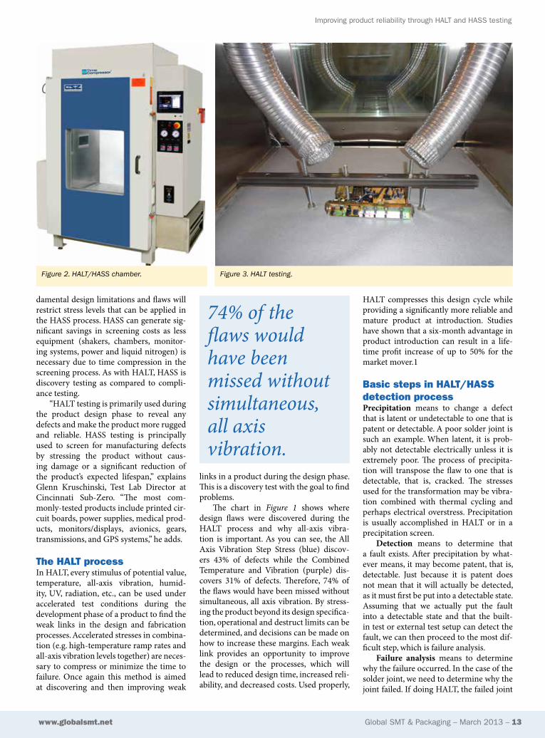
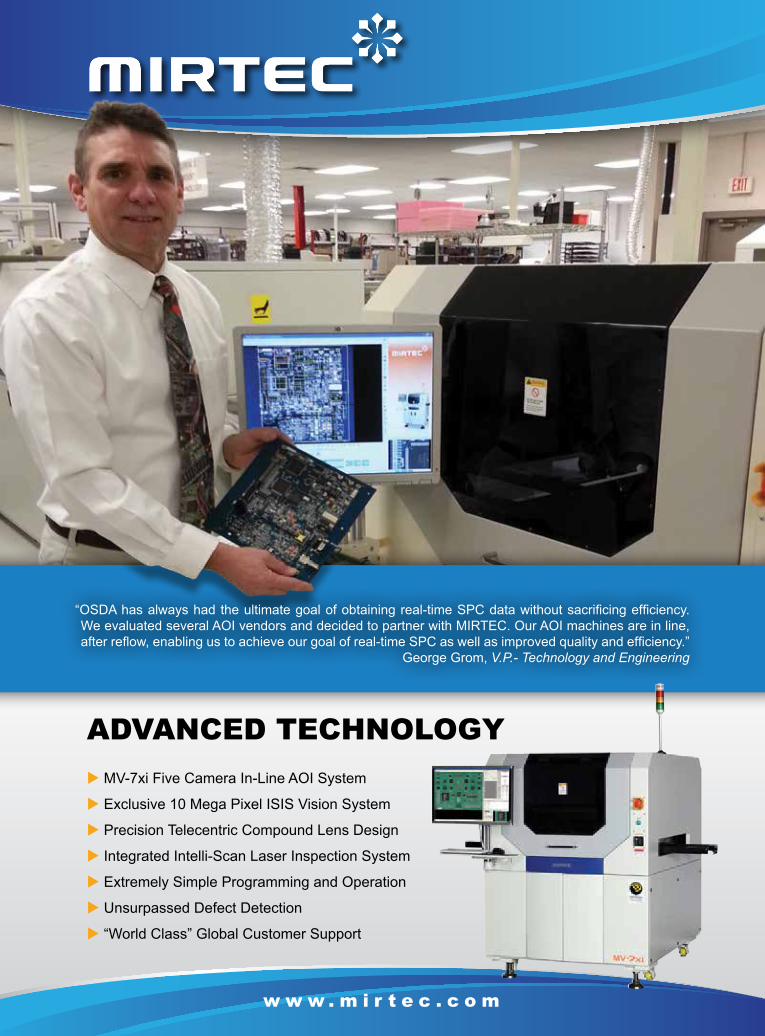
Figure 2. HALT/HASS chamber. Figure 3. HALT testing.

14 – Global SMT & Packaging – March 2013 www.globalsmt.net
Improving product reliability through hALT and hASS testing
could be due to a design flaw; that is, an extreme stress at the joint due to vibration or possibly due to a poor match of thermal expansion coefficients. When doing HASS, the design is assumed to be satisfactory (which may not be true if changes have occurred) and in that case, the solder joint was probably defective. In what manner it was defective and why it was defective needs to be determined in sufficient detail to perform the next step, which is correc-tive action.
Corrective action means to change the design or processes as appropriate so that the failure will not occur again. This step is absolutely essential for success. In fact, corrective action is the main purpose of performing HALT or HASS. One of the major mistakes happening in the industry is that manufacturers “do HALT” and dis-cover weaknesses and then dismiss them as due to overstress conditions. It is true that the failures occurred sooner than they would in the field, due to the overstress conditions, but they would have eventually occurred in the field at lower stress levels.
Verification of corrective action needs to be accomplished to determine that the product is really fixed and that the flaw that caused the problem is no longer present. The fix could be ineffective or there could be other problems causing the anomaly that are not yet fixed. Additionally, another fault could be induced by operations on the product, and this necessitates a repeat of the conditions that prompted the fault to be evident. One method of testing a fix during the HALT stage is to perform HALT again and determine that the product is at least as robust as it was before and it should be somewhat better. If in the HASS stage, performing HASS again on the product is in order. If the flaw is correctly fixed, then the same failure should not occur again.
The last step of the six is to put the
lesson learned into a database from which one can extract valuable knowledge whenever a similar event occurs again. Companies that practice correct HALT and utilize a well-kept database soon become very adept at designing and building very robust products with the commensurate high reliability.1
Comparing hALT and hASS chambersThere are many factors that need to be con-sidered when evaluating a HALT chamber purchase. One of the first obvious criteria is to look at a size that will handle the size of your DUT. Other factors to consider are the high and low vibration limits of the chamber, and the characterization of the table (how well is the vibration dis-tributed). A safety door interlock system should be in place to prevent the door from being open when liquid nitrogen is flowing into the chamber. It would also be useful to have multiple cable ports for any con-nections you need to make to your DUT, and front and rear doors on the larger size units. You will also want to check out the nitrogen and compressed air usage along with their sound levels.
With liquid nitrogen being the cooling media predominantly used in HALT test-ing, you need to consider how many tests you will be running per day, per month, to try to get a handle on the amount of liquid nitrogen that will be required, as you do not want to run out during the middle of a test. You can then contact a local gas supplier to find out what is the most cost effective solution to choose. If you cur-rently have a source of liquid nitrogen in your facility, you will need to find out where it is located and where you plan to locate your chamber. Running the vacuum jacketed connection lines from the source to the chamber is very expensive (estimates
at approximately $200/running foot). It is also a good idea to put an oxygen sensor in your lab, in the event that too much nitro-gen is escaping into the lab.
An ideal situation is to be able to run your DUT on a chamber before you make a purchase decision. Many chamber manu-factures will have a chamber available for your use and I would suggest that you take them up on their offer. This will also give you an opportunity to determine what fix-tures will be necessary. They can also guide you through the first steps in setting up your HALT test.
Using fixturing that does not transmit the stress to the product under test can be a problem because sufficient levels of stress never reach the product. Three examples are: 1. Using a vibration fixture that will not
transmit the frequencies associated with critical modes of vibration of the product under test or isolates the mid-and high-ranges.
2. Using a thermal fixture that does not transmit the conditioned air to the product such that the product can be rapidly changed in temperature over a broad range.
3. Using electrical overstress and having some circuitry such as the lightning arrestor circuitry bleed off the high voltage before it gets to the internal circuits.
4. If the stress does not get to the product, then nothing has been accomplished.2
The basic steps of hALT Determination of operational and destruct limits for temperature and vibration is an important part of HALT. Some companies do not test to destruction due to the high costs of test units (like aerospace prod-ucts). Some engineers incorrectly think
Figure 4. Operating & destruct limits. Figure 5. Low temp test graph [IPC-9592A].
Continued on page 46
Troubleshooting SMT Assembly?
Interface Analysis Software enables In-Depth review of the attachment interface between two surfaces, such as package to PCB
For a white paper on this subject send an email to: [email protected]
Dual Surface Comparison at Any Temperature
Shape Matching Identifies Where Defectsare Likely to Appear Gap and Root Cause Analysis _ Process Control
akrometrix-GSP13.7.indd 1 6/18/13 9:16 AM

16 – Global SMT & Packaging – March 2013 www.globalsmt.net
Anthropologists believe that the great plagues of the middle ages can be attrib-uted, in part, to the decline in cleanliness standards including personal hygiene in that era. It seems that throughout history, the lack of cleanliness results in undesirable outcomes. Ironic, to say the least, is the fact that in our modern society cleanliness is valued greatly. There is, however, one area in which we pay little attention to cleanli-ness. This area affects almost every aspect of our lives. This area affects how we com-municate, travel, protect ourselves, play, work, eat, and even how we access medi-cal care. This area is electronics. It is nearly
impossible to think of life without electron-ics. We depend on electronics assemblies in nearly every aspect of our lives. Why then do we not demand a higher level of cleanli-ness with electronics assemblies?
Unfortunately, the answer to that ques-tion is common. When industry-favorite solvents were banned due to environmental concerns in 1989, the industry, rather than switching to environmentally responsible alternative solvents chose instead to adopt a no-clean approach. New low-residue flux formulations were introduced, leaving only small amounts of flux residue on the assem-blies. The volume of residues left on the
Over the past 28 years, the electronics assembly cleaning industry has gone through three distinct periods. There was the period before 1989 when virtually all assemblies were cleaned after soldering. Then there was the period between 1989 and 2005 when cleaning was the nearly exclusive realm of military, aerospace and medical (high-reliability assemblers). Now is the current period—2005 to present—where, according to industry poles, two thirds of all assemblers are cleaning their assemblies and 52 percent of all no-clean solder paste applications result in cleaning.
Mike Konrad, Aqueous Technologies Corporation
Why no-clean cleaning works today
why no-clean cleaning works today

Global SMT & Packaging – March 2013 – 17www.globalsmt.net
why no-clean cleaning works today
assemblies was, at that time, considered to be acceptable. The industry weighed the cost of switching to alternative sol-vents and compatible equipment against accepting small amounts of residues on assemblies. Cost savings won. But not everyone abandoned cleaning. Military, medical, aerospace and other high-reli-ability maintained a cleaning program. Most of these industries switched to alternative cleaning technologies, most often aqueous-based cleaning methods. It seems that cleaning is required only when reliability is paramount.
This dual alternate universe, 100 percent cleaning of every assembly with high-reliability assemblers vs. 100 percent not-cleaning of commercial assemblers, lived mostly happily side by side for many years. Over time, however, many commer-cial assemblers have adopted a cleaning process. As referenced earlier, two thirds of all assemblers state that they clean between 25-100 percent of their assemblies. Of the multitude of commercial assemblers using no-clean solder pastes, 52 percent of them are cleaning after reflow. What is the driver for the rapid rise in the amount of assem-blers adopting or readopting a cleaning process?
There are many factors that drive our industry back to cleaning. In fact, the pri-mary driver is identical to the one that, 24 years ago, steered assemblers away from cleaning in the first place—economics.
One frequently overlooked factor is that when assemblers stopped remov-ing flux from their assemblies due to the implementation of low-residue fluxes, all cleaning stopped. Contamination from the bare board fabrication, component fabrica-tion and assembly processes were allowed to remain on the assembly along with flux residues. The fact is that modern miniatur-ized, lead-free assemblies cannot tolerate as much contamination as assemblies of the past. Smaller assemblies, higher den-
sities, lower component standoff heights, faster speeds, and higher reflow tempera-tures all combined to create the perfect storm of events that are causing electrical migration and electrical leakage failures on assemblies throughout the world. In field assembly, failure is costly in terms of both economic and reputation concerns. A measurable percentage of the electron-ics industry has determined that it is more cost effective to remove contamination than to reap the cost of contamination-related failures.
There are many perceived challenges when one considers the adaptation of
a cleaning process: What is the cost of cleaning (cost per assembly)? What is the cost to the environment (kudos to those who consider the environment)?
So, what is the cost of cleaning? Many assemblers have discovered that it is sur-prisingly low. There are many cleaning methods, machines and processes avail-able from which to choose. The correct specific method is determined by several variables including desired throughput, types of contamination being removed, environmental restrictions, etc. While there is no “one size fits all” solution, there are a handful of solutions that fit almost all assemblers. We spend a lot of time talking about a “properly optimized pro-cess” (the correct machine to match the
required throughput, equipment readiness, cleanliness requirement and discharge configuration). When one has a properly optimized process, one may expect total cleaning costs per assembly to be under USD $0.06 per assembly for low discharge cleaning applications (environmentally beneficial) to USD $0.16 per assembly for zero-discharge (environmentally respon-sible).
Many assemblers have resisted clean-ing processes for strictly environmental reasons. Many have been concerned that by solving one issue (assembly failures), they would exchange that issue for another (environmental regulatory issues). The fact is that recent advances in cleaning tech-nology have allowed assemblers to clean assemblies, regardless of flux type, and operate in a completely zero-discharge configuration. By operating a cleaning process that reuses the cleaning chemical, lowering operational costs, without a con-nection to a drain, and bypassing environ-mental regulations, one can experience an optimized cleaning process that eliminates contamination-caused assembly failures while obtaining an acceptable cost per cleaned assembly, and a total avoidance of environmentally-based regulation. This is a win-win scenario.
Mike Konrad is President and Founder of Aqueous Technologies, a California-based manufacturer of automated cleaning/defluxing equipment and cleanliness testing equipment. Mike travels the world teaching cleaning and reliability workshops, provid-ing valuable cleaning process information to companies wishing to implement clean-ing processes. Mike can be reached at 9055 Rancho Park Ct., Rancho Cucamonga, CA 91730; 909-944-7771E-mail: [email protected]; Web site: www.aqueoustech.com.
So, what is the cost of cleaning? Many assemblers have discovered it is surprisingly low.

18 – Global SMT & Packaging – March 2013 www.globalsmt.net
Still waiting for a solid upturn
The much-awaited 2013 “global recovery” experienced some regional setbacks this spring. Based upon May PMI leading indi-cator data (Chart 1) the world is just barely in a growth mode with Japan and Europe reporting improved Purchasing Managers’ Indices, China, Taiwan and S. Korea seeing weakening and the USA falling back into contraction.
On a 3/12 growth basis (Chart 2) key components of the electronic supply chain (semiconductors, PCBs and electronic equipment) have had declining revenues with their leading indicator pointing to minimal growth (excluding seasonality) in the near term.
Global electronic equipment produc-tion (Chart 3) suffered in early 2013 and sales results through April showed only a modest seasonal “electronics end market” recovery.
In the USA most of the electronic supply chain has been contracting in 2013
(Chart 4) with military electronics (Chart 5) being especially hard hit. One encour-aging sign was the April improvement in measurement and control equipment orders (Chart 6) but overall domestic elec-tronics demand has been weak.
In SE Asia suppliers are being forced to adjust to diminished personal computer demand as tablets and smartphones have assumed the roles of many traditional PCs (Chart 7).
World semiconductor demand remained flat through April with Custer Consulting Group’s semiconductor leading indicator pointing to minimal improve-ment over the next few months (Chart 8). The recent WSTS update of its semiconduc-tor forecast (Chart 9) now predicts growth of world chip shipments to be only +2% in 2013 (followed by +5% next year).
In summary 2013 is not shaping up as the solid growth year that was hoped. We will see a normal seasonal expansion this
summer and autumn but robust year-on-year expansion still remains elusive.
End marketsIT spending expectations were lowered to 4.9% growth by IDC as sequester and global economic uncertainty diminished business confidence.Mobile Communications• Mobile phone sales increased 0.7% y/y
to nearly 426 million units in 1Q’13. More than 226 million mobile phones were sold in Asia/Pacific.—Gartner
• Global handset touch panel shipments are expected to grow 5.5% q/q to 284 million units in 2Q’13.—Digitimes Research
• Global smartphone shipments are expected to reach 937 million units in 2013.—NPD DisplaySearch
• NFC (Near Field Communication) enabled cell phone shipments will reach 1.2 billion units from 2012 through 2017.—IHS subsidiary of IMS Research
Computers & Peripherals• Notebook touch screen shipments
increased 51.8% q/q to 57 million units in 1Q’13.—Displaybank
• Worldwide PC shipments are expected to fall by 7.8% y/y in 2013 as market shifts to tablets.—IDC
• Worldwide tablet shipments are expected to grow 58.7% y/y to 229.3 million units in 2013.—IDC
• Worldwide server shipments declined 0.7% y/y to 2.3 million units in 1Q’13.—Gartner
• Personal & entry level storage market grew 73.4% y/y with 20.2 million units shipped in 1Q’13.—IDC
• Taiwan’s contract notebook shipments are forecast to drop 9% y/y in 2013.—SinoPac Securities
Data Communications• Optical network hardware market
(including SONET/SDH and WDM equipment) totaled $2.6 billion in 1Q’13.—Infonetics Research
• Home networking device market increased 5% y/y to $4.9 billion in 2H’12.—Infonetics Research
Walt Custer and Jon Custer-Topai
Still waiting for a solid upturn
51.1
50.7
52.6
50.4
46.7
50.7
50.4
51.5
47.1
51.1
49.2
48.3
49.0
50.6
45.0 47.0 49.0 51.0 53.0 55.0
Japan
Taiwan
S Korea
China
Europe
USA
World
PMI
May April
Purchasing Managers' Indices May vs. April 2013
Markit Economics, JPMorgan and ISM
Above 50 = GrowthBelow 50 = Contraction
20130603
Chart 1.

Global SMT & Packaging – March 2013 – 19www.globalsmt.net
Still waiting for a solid upturn
• Internet of Everything to grow from more than 10 billion wirelessly con-nected devices in 2013 to over 30 bil-lion devices in 2020.—ABI Research
• Enterprise videoconferencing and tele-presence equipment market revenue declined 13.2% y/y to $563.4 million in 1Q’13.—IDC
Other• Automotive electronics market is set to
rise more than 50% from $157 billion in 2010 to $240 billion in 2020.—IMS
• LED light bulb shipments are forecast to increase 151% y/y to 842 million units in 2013.—Digitimes Research
• LCD monitor OEM shipments decreased 13.9% y/y to 33.1 million in 1Q’13.—TPV
• Touch-screen panel shipments will double from 2012 to nearly 3 billion units in 2016.—IHS
• Large-area TFT LCD revenue is expected to fall 2% y/y-from $83.6 bil-lion in 2012 to $81.7 billion in 2013.—NPD DisplaySearch
• Hardcopy peripherals market decreased 9.7% y/y with 25.8 million units shipped in 1Q’13.—IDC
• Large format printer market declined 12.0% y/y in 1Q’13 on shipments of approximately 75,000 units.—IDC
EMS, ODM & related assembly activityMedical industry EMS opportunities will grow from $16.43 billion in 2012 to $34.38 billion in 2019.—Frost & SullivanBittele Electronics began offering proto-type PCB assembly services.Cirtronics added two Pillarhouse Jade selective solder machines, two MY100DX pick and place machines and a PDR IR-C3 Chipmate SMT rework system.Connor Solutions appointed Steve
Henderson as Business Development DirectorCreation Technologies’ facility in Ontario, Canada achieved FDA registration.Dorigo celebrated 25 years as an EMS pro-vider.EastBridge Engineering established its Design Launch division.EMS Solutions moved into a 45,000 SF facility in Business Depot Ogden in Ogden, Utah.Engent joined the High Density Packaging User Group.Escatec • added a Nikon XTV160 2.5D X-Ray
inspection system.• appointed Johan Halling, GM of
Escatec Electronics and Escatec
Medical in Penang, Malaysia.Flextronics spent $25 million on improve-ments and equipment at its 445,870 SF Fort Worth, Texas facility, which began smart-phone assembly for Motorola.Foxconn/Hon Hai • acquired technology for carbon nano-
tube touch panel production.• became major investor in Tai Tung
Communication’s fiber-optic JV.• opened a display R&D center in Sakai
City, Japan.• partnered with PT Erajaya Swasembada
to build a factory to produce mobile phones, tablets and other telecommu-nication products in Indonesia.
• was ranked 5th among top 1,000 firms in Greater China.—CommonWealth Magazine poll
Global PMI, Electronic Equipment, PCB & Semiconductor Shipments
20130606
0.4
0.6
0.8
1.0
1.2
1.4
1.6
1.8
Mar
Jun
Sep
Dec Mar
Jun
Sep
Dec Mar
Jun
Sep
Dec Mar
Jun
Sep
Dec Mar
Jun
Sep
Dec Mar
Jun
Sep
Dec Mar
Jun
Sep
Dec Mar
Jun
Sep
Dec Mar
Jun
Sep
Dec Mar
Jun
Sep
Dec Mar
Jun
Sep
Dec Mar
Jun
Sep
Dec Mar
Jun
Sep
Dec Mar
Jun
00 01 02 03 04 05 06 07 08 09 10 11 12 13
PCBSIAEl EquipGlobal PMIZero Growth
3/12 Rate of Change
Source: Custer Consulting GroupCalendar Year
Chart 2.
Latest Annual 3-Month Month Growth Growth
Electronic Component $Rigid PCB Orders (N Amer) 4/13 97.8 99.6Rigid PCB Shipments (N Amer) 4/13 94.3 92.7Flex Circuit Orders (N Amer) 4/13 90.0 91.9Flex Circuit Shipments (N Amer) 4/13 103.3 100.4Electronic Component Orders 4/13 98.9 97.0Electronic Component Shipments 4/13 97.8 94.2Semiconductor Shipments to N America 4/13 99.2 95.7
U.S. Electronic Equipment Orders $Computer & Related 4/13 99.5 96.6Communication 4/13 104.5 97.1Medical, Measurement & Control 4/13 89.2 87.5Search & Navigation 4/13 89.6 80.7Defense Capital Goods 4/13 101.9 80.7Military Electronics 4/13 83.9 77.5Total Electronic Equipment 4/13 94.1 89.1
U.S. Industrial Production 4/13 103.0 102.5
NOTE: 3 month growth rates compare most recent 3 months to same 3 months one year earlier
Present Growth Rates (%)20130606
U.S. Economy & Electronics IndustryWorld Electronic Equipment Monthly
ShipmentsConverted @ Constant 2010 Exchange Rates
Source: Custer Consulting Group
20130605
80
90
100
110120
130
140
150
160170
Jan
May
Sep
Jan
May
Sep
Jan
May
Sep
Jan
May
Sep
Jan
May
Sep
Jan
May
Sep
Jan
May
Sep
Jan
May
Sep
Jan
May
Sep
Jan
May
Sep
Jan
May
Sep
Jan
May
Sep
Jan
May
Sep
Jan
May
2000 2001 2002 2003 2004 2005 2006 2007 2008 2009 2010 2011 2012 2013
Thou
sand
s
US$ B
Chart 3. Chart 4.

20 – Global SMT & Packaging – March 2013 www.globalsmt.net
Still waiting for a solid upturn
Inovar appointed Gene Sparks as Southwest U.S. Sales Director.Lacroix appointed François Beauxis as Managing Director of its electronics divi-sion.PCA Technology was acquired by MSKK Investments.Pegatron plans to hire 40,000 new workers in 2H’13.Pektron Group upgraded two production lines that include six Hitachi Sigma Series machines in Derby, UK.Power Design Services achieved ITAR compliancy under the U.S. Department of State.Proto-Pac Engineering leased a 42,872 SF manufacturing building in Wilmington, MA.
Saline Lectronics appointed David Cusumano, VP of Engineering.Sanmina received a contract to provide the majority of repair services for Motorola Solutions.Season Group acquired Outsource Electronics Limited.SMTC appointed Larry Silber as Interim CEO, Clarke Bailey as Executive Chairman and Steve Brown as VP, Quality and Engineering.TT electronics-IMS division merged with New Chapel Electronics.
PCB fabricationFlexible devices (primarily flexible printed circuits) manufactured by roll-to-roll technologies will grow from $10.8 billion
in 2012 to nearly $22.7 billion by 2017.—BCC ResearchPrinted, flexible and organic electronics will grow at a 15.3% CAGR from $16.04 billion in 2013 to $76.79 billion in 2023.—IDTechExTaiwan PCB production value is expected to rise 3% q/q to NT$119 billion (US$4 bil-lion) in 2Q’13.—IEKAsian Circuits launched a turn-key PCB assembly service.AT&S plans to close its Klagenfurt plant at the end of 2013.Farnell and Eurocircuits entered quick-turn bare board PCB prototyping services collaboration.Invotec Group appointed John Fitzpatrick, Sales Account Manager for South East UK.MTI Electronics installed an AOI system.Stevenage Circuits added an Orbotech Sprint 120 ink jet legend printing machine.Sumitomo Electric • developed thin construction for flex-
ible circuits filling via holes with con-ductive nano paste.
• began mass-production for new type FPCs at Minakuchi Works.
Würth Elektronik began offering wire bonding service.
Materials & process equipmentGlobal laser materials processing systems market grew 9% y/y to €7.9 billion in 2012 (market grew 1% when measured in US-dollars)—Optech ConsultingOLED materials market will grow from $450 million in 2013 to over $4.6 billion by 2021.—NanoMarketsTaiwan’s specialty chemicals output will grow 6% y/y to NT$678.54 billion (US$22.79 billion) in 2013.—Industry and
U.S. Electromedical, Measurement & Control EquipmentOrders & Shipments
www.census.gov/indicator/www/m3/
20130605
4
5
5
6
6
7
7
8
8
Jan
May
Sep
Jan
May
Sep
Jan
May
Sep
Jan
May
Sep
Jan
May
Sep
Jan
May
Sep
Jan
May
Sep
Jan
May
Sep
Jan
May
Sep
Jan
May
Sep
Jan
May
Sep
Jan
May
Sep
Jan
May
Sep
Jan
May
Sep
Jan
May
1999 2000 2001 2002 2003 2004 2005 2006 2007 2008 2009 2010 2011 2012 2013
Orders
Shipments
$ Billions (monthly, seasonally adjusted)
Chart 6.
U.S. Military Electronics Orders & ShipmentsDefense Communication & Search & Navigation Equipment
www.census.gov/indicator/www/m3/
20130605
0
1
2
3
4
5
6
Jan
May
Sep
Jan
May
Sep
Jan
May
Sep
Jan
May
Sep
Jan
May
Sep
Jan
May
Sep
Jan
May
Sep
Jan
May
Sep
Jan
May
Sep
Jan
May
Sep
Jan
May
Sep
Jan
May
Sep
Jan
May
Sep
Jan
2000 2001 2002 2003 2004 2005 2006 2007 2008 2009 2010 2011 2012 2013
Thou
sand
s Orders
Shipments
$ Billions (monthly, seasonally adjusted)
Chart 5.
Media Tablet Shipmentsto End Users by Operating System
Gartner 4/12
20121027
2011 2012 2013 2014 2015 2016Other 1,919 510 637 464QNX 807 2,643 6,036 17,836Microsoft 0 4,863 14,547 43,648Andoid 17,292 37,878 61,684 137,657iOS 39,998 72,988 99,553 169,652
0
50,000
100,000
150,000
200,000
250,000
300,000
350,000
400,000Units
Chart 7.
w w w . m i r t e c . c o m
u MV-7xi Five Camera In-Line AOI System
u Exclusive 10 Mega Pixel ISIS Vision System
u Precision Telecentric Compound Lens Design
u Integrated Intelli-Scan Laser Inspection System
u Extremely Simple Programming and Operation
u Unsurpassed Defect Detection
u “World Class” Global Customer Support
ADVANCED TECHNOLOGY
“OSDA has always had the ultimate goal of obtaining real-time SPC data without sacrificing efficiency. We evaluated several AOI vendors and decided to partner with MIRTEC. Our AOI machines are in line, after reflow, enabling us to achieve our goal of real-time SPC as well as improved quality and efficiency.” George Grom, V.P.- Technology and Engineering
MW-MI-21-OSDA_Testimonial_203x275.indd 1 3/25/13 10:46 AM

22 – Global SMT & Packaging – March 2013 www.globalsmt.net
Still waiting for a solid upturn
Technology Intelligence ServicesAgfa Materials appointed Rich Breitlow, Channel Sales Manager for North AmericaAgilent laid-off 450 workers.Aismalibar North America named Gareth Parry, Chief Field Application Engineer.Bayer MaterialScience inaugurated a regional innovation hub in Shanghai.Cambridge Nanotherm is building a nanoceramic-aluminium substrate proto-type manufacturing plant in Haverhill, UK.Chomerics achieved ISO 14001: 2004 certification for its facility in Saint Ouen l’Aumone, France.Dymax named Marufur Rahim, R&D Manager and Margo Martin, Global Account Manager.Equipment Technologies merged with North East Automation.Finetech & Martin named Al Cabral, Regional Sales Manager.GT Advanced Technologies acquired Thermal Technology.H.B. Fuller entered electronics and assem-bly materials market with total solutions “eco-system” approach that includes mate-rials, processes and equipment.Isola enhanced its Quick Turnaround Service in Europe.Manncorp moved into its 18,000 SF headquarters in Huntingdon Valley, Pennsylvania.MYDATA Royonic moved into new offices in Unterhaching, Germany.Optomec is developing new digital pro-duction solution that enables direct print-ing of antennas used in mobile device applications.Park Electrochemical appointed Linda Lagnese, Director of Human Resources.SIPLACE appointed Technica USA as its new sales partner for its SMT place-ment equipment, software and services in
Western USA.Teledyne acquired Axiom IC.ZESTRON appointed Stefan Theil, Regional Sales Manager for South Germany.
Semiconductors & other componentsChina electronic components distributors expect 23% revenue growth in 2013.—Global SourcesEuropean semiconductor distribution sales fell 5% y/y to 1.48 billion Euros in Q1/CY13.—DMASSIC Insights lowered its forecast for 2013 semiconductor market from 6% to 5%, citing tepid 1Q’13 GDP estimates in many of the world’s largest economies.North American semiconductor equip-ment industry posted $1.17 billion in orders worldwide in April 2013 (3-month average basis) and a book-to-bill ratio of 1.08.—SEMICombo MEMS sensors used in motor vehicles are expected to grow by 77% y/y from $92 million in 2012 to $163 million in 2013.—IHS iSuppli
Global nanomagnetic materials and devices market will reach $9 billion by 2017.—BCC ResearchiNEMI published its tenth roadmap.Smart grid sensor market is expected to top $100 million in 2015.—IHSTaiwan-based IC design houses’ ship-ments grew 21.6% y/y to NT$20.18 billion (US$673.8 million) in 1Q’13.—Digitimes ResearchTotal MPU sales will grow 10% y/y to $62.0 billion in 2013.—IC InsightsWorldwide semiconductor market contracted 2.2% y/y in 2012 to $295 billion however 3-4% revenue growth is expected in 2013.—IDC
Worldwide silicon wafer area shipments increased 4.8% y/y to 2,128 million square inches in 1Q’13.—SEMI
Walt Custer is an independent consultant who monitors and offers a daily news service and market reports on the PCB and assembly automation and semiconductor industries. He can be contacted at [email protected] or visit www.custerconsulting.com.
Jon Custer-Topai is vice president of Custer Consulting Group and responsible for the corporation’s market research and news analysis activities. Jon is a member of the IPC and active in the Technology Marketing Research Council. He can be contacted at [email protected].
Worldwide Semiconductor Market by GeographyWSTS Forecast
WSTS 6/13
20130604
1999 2000 2001 2002 2003 2004 2005 2006 2007 2008 2009 2010 2011 2012 2013 2014 2015Asia Pacific 37.2 51.3 39.8 51.2 62.8 88.8 103.5 116.5 123.5 124.0 119.6 160.0 164.0 163.0 172.2 182.7 191.4Japan 32.8 46.7 33.1 30.5 38.9 45.8 44.1 46.4 48.8 48.5 38.3 46.6 42.9 41.1 35.4 36.8 37.6Europe 31.9 42.3 30.2 27.8 32.3 39.4 39.1 39.9 41.0 38.2 29.9 38.1 37.4 33.2 34.9 36.3 37.4Americas 47.5 64.1 35.8 31.3 32.3 39.1 40.7 44.9 42.3 37.9 38.5 53.7 55.2 54.4 55.2 57.1 58.5
0
50
100
150
200
250
300
350
Chart 9.
CCG Semiconductor Leading Indicator vs. Global Semiconductor Shipments
http://www.census.gov/indicator/www/m3/
20130606
0.3
0.5
0.7
0.9
1.1
1.3
1.5
1.7
Jan
May
Sep
Jan
May
Sep
Jan
May
Sep
Jan
May
Sep
Jan
May
Sep
Jan
May
Sep
Jan
May
Sep
Jan
May
Sep
Jan
May
Sep
Jan
May
Sep
Jan
May
Sep
Jan
May
Sep
Jan
May
Sep
Jan
May
2000 2001 2002 2003 2004 2005 2006 2007 2008 2009 2010 2011 2012 2013
CCG Semiconductor Leading Indicator
SIA Semiconductor Shipments
0 Growth
3/12 rate of growth2-MonthLead
Chart 8.
China electronic components distributors expect 23% revenue growth in 2013.

Summer 2013
USING ThERMAL SIMULATION AND ChARACTERIzATION TO IM-PROVE LED PRODUCT DESIGN • KEVIN WILLMORTh TALKS SSL INDUSTRy ChALLENGES • INDUSTRy NEWS
www.globalledoled.com
seLeCtING tHe rIGHt drIVer For yOUR LED APPLICATION
Special Supplement

Title
24 – Global LED/OLED Supplement — Summer 2013 www.globalledoled.com
Editorial OfficesEuropeTrafalgar Publications Ltd.Global LEDs/OLEDs MagazineCrown House, 72 Hammersmith Rd,London, W14 8THUnited KingdomTel: +44 (0) 207 559 1467Fax: +44 (0) 207 559 [email protected]: www.globalledoled.comUnited StatesGlobal LEDs/OLEDsPO Box 7579Naples, FL 34102, USATel: +1 239 245-9264Fax: +1 239 [email protected] Trevor GalbraithTel: +1 (239) 245-9264 x101 (US)Tel: +44 (0)7584 072926 (UK mobile)Tel: +1 (239) 287 5401 (US mobile)[email protected] ChasonTel: +1 224 659 2446 (US)[email protected] EditorTel: +1 239 245-9264 ext. 108 (US)[email protected] Development /Marketing ManagerElisangela DahlkeTel: +1 239 245 9264 ext. 110 (US)Cell: +1 239 287 5398 (US)Cell: +44 7924 554456 (UK)[email protected] DeveloperTorrence GermanyTel: +1 239 245 9264 ext. 105 (US)[email protected]
Circulation & SubscriptionsTel: +1 239 245 [email protected]
AdvertisingSales Representative—North AmericaSandy Daneau Tel: +1 239 245 9264 ext. [email protected]
Sales Representative—Europe & AsiaElisangela DahlkeTel: +1 239 245 9264 ext. 110 (US)Cell: +1 239 287 5398 (US)Cell: +44 7924 554456 (UK)[email protected]
Editorial
Marc ChasonEditor-In-Chief
Migrating from significant R&D investments to viable products is often a manu-facturing challenge. What processes and technologies can be used to expedite the process? How can supply chains, which are usually slow to develop, rapidly
grow to catch up to their industries needs? Roadmaps can point out the directions the industry is moving towards, but implementation is still required.
The Solid State Lighting industry is undergoing such a transition. In addition to the rapid progress in LED efficacy, which enables SSL products, numerous other processes and technologies are being developed to further drive down product costs. Will these efforts be more focused on the SSL light engine, or the more traditional luminaire manufacturer? For example, companies such as Molex, TE, Ideal and others are making replacement bases (essentially SSL “Edison” bases if you will) in an effort to bring more SSL specific function-ality to the customer.
SSL system solutions are being designed with increasing complexity. Taking on increased significance are designs for more efficient LED drivers, the need to dissipate increasing levels of heat for long-lived robust products, the use of remote phosphors to improve light output (and enable Design for Postponement) are examples of the need for fast-paced product implementations. Coupling this with standards, which can be a key driver for SSL product introduction, reveals the need for speedy implementation pathways for new technology. With an abundance of new designs, how does the industry insure com-patibility with rapidly evolving standards? Or should it at this early stage of development?
András Poppe’s article on software modeling tools addresses some of these concerns. In his article, “Using Thermal Simulation and Characterization to Improve LED Product Design,” he demonstrates how software modeling tools can improve the design cycle by removing added time and costs associated with prototyping builds and tests. This is not just for new designs but for improving all aspects of the design process.
Similarly, Osama Mannan’s article, “Selecting the right driver for your LED applica-tion,” focuses on designing LED drivers. As demonstrated in Mannan’s article, software modeling is a key technology to enable sorting through multiple technical options to focus on a preferred solution.
Kevin Willmorth provides a provocative and thought provoking interview as he dis-cusses the state of the SSL supply chain and its successes and misses in supporting this new technology.
As the drivers to reduce SSL system cost continue to accelerate, new software tools and concepts continue to emerge to help drive the process. With these tools, SSL should be a win/win for both customers and manufacturers.
—Marc Chason
SSL tools for driving the supply chain

Global LED/OLED Supplement — Summer 2013 – 25www.globalledoled.com
Title
The lighting market is an odd confluence of individuals and business models that is difficult
to grasp at times. From the single person custom shops serving select customers to the massive multi-national conglomerates battling it out for market share, there exists an almost infinite array of players in this game. Business in the lighting market can take the form of artisan shop, energy saving company, electrical contractor, design-build firm, design consultancy, small-scale focused market space producer, mass commodity manufacturer, distributor, environmental agency, a lighting maintenance company, independent sales agency, or a blend of these. It’s an intriguing market space. The injection of solid-state lighting has expanded this further, injecting its own brand of diversity and technology into the already colorful matrix. While some argue that the end is near for the niche player in the new frontier of lighting founded on technology, those who really know lighting are unconvinced.
Beyond the ubiquitous discussions of core technology, lighting is not about installed hardware, it’s about delivering light. The human visual system has no sensor to qualify efficiency, environmental impact, or merits of one technology over another. This is a source of disconnect within the industry and where newcomers get mired. Even before SSL, there are those who see lighting as a product market, separate of the applied impact those products have on human occupants. This is a case where even if the majority fails to realize it, lighting is not a hardware business, it is a vision business. This disconnect is a constant source of frustration for those focused on application of light itself. The tug of war between delivering the best
visual environment and available (read affordable) hardware is a constant. For this reason, manufacturers find frustration in their attempts to satisfy the desires of the design community, who seem to have an infinite pool of esoteric small ideas difficult to support with mass production. To avoid this quagmire, SSL developers may find success focusing on the mass market products – replacement lamps, linear strips, and other easy to identify existing categories. In time these spaces will produce a declining return on investment due to over-saturation. When this happens, and it will, the focus will be on finding new solutions, and the design influencers will be one place to find them.
Solid-state lighting delivers a contradiction of realities. Light sources of very small scale, optically controllable, with impressive efficiency in a form factor that lends itself to diversity and custom source forms is exciting news to lighting experts. The potential for creating all new forms, to deliver the right light, where it is needed, tuned with precision, is exciting and inspiring. Yet, contrasting this is the demand for mass production that stifles customization potential. SSL comes from a universe used to massive production scale, through channels that thrive on large customer repeat orders. The end result is the single greatest technology to come to light in the last century is bottled up inside business models that make utilizing its greatest potential very difficult (read expensive) if not impossible. Pile on a few new difficult (expensive and time consuming) standards and test protocols, and you have the proverbial wet blanket effect.
If anyone is looking for a reason why SSL has not simply run all other technologies
off the road, this is it. In this diverse market there is a need for more. Specifically, there is a need for new models, new entities that can connect the massive potential of the technology, with the even greater potential for applying it in diverse, small scale, niche and specialty products that deliver the precision and flexibility that makes it so exciting. Should the SSL technologists and marketers embrace, rather than fight, the diversity of the lighting market, the potential for an all-out revolution is there to be had. Every major lighting product category today came from a period of rabid innovation by small entities that expand and transform markets. This demands support for innovators. While mass quantities in the short term may come from redressing what has already been done with new sources, ultimately it will be breakouts in new product concepts that will turn the market and generate a real transformation that will put the past in its proper place.
Kevin has been involved in lighting for over 30 years, with experience in design consulting, product development and editorial/technical writing. He currently owns Lumenique, LLC providing design and strategic consulting to luminaire and SSL technology providers, and is editor of Architectural SSL magazine.
Kevin Willmorth
The need for new models to
support lighting market diversity
Inside Solid-State Lighting
26 – Global LED/OLED Supplement — Summer 2013 www.globalledoled.com
Selecting the right driver for your LED application
Selecting the right driver for your LED application
Key parameters of an LED driverWhile each driver can have different speci-fications and functionalities, all of them have a set of common parameters. The light output of an LED is a function of current. Therefore, LEDs must be supplied wit ha constant current to give out constant light output. Furthermore, LEDs are typically low voltage devices, so an LED driver needs to provide them with the sufficient DC volt-age they need. An LED driver basically con-verts the input voltage, whether AC or DC, to a DC voltage with a con-stant current output to supply the LEDs, as shown in Figure 1. Depending on the input source, the driver will either convert an AC input to a DC output, or adjust a DC input voltage to one that better matches the total voltage required by the LEDs.
In the case of an AC-to-DC driver, the input voltage that each driver can accept depends on the region it will be used in. For example, in North America the AC line voltage is in the 110-120VAC range, so North American drivers will accept an input voltage in that range and convert it in to DC voltage. Similarly, a European driver will accept a voltage range of 220-240VAC and convert it to DC voltage. Furthermore, there are drivers, called Universal drivers, that can be used in different regions, and
may have an input voltage range of 110-240VAC or even up to 277VAC depending on their capability.
In addition to the input voltage, the output voltage is also as important to define the usage of an LED driver. The output voltage range determines how many LEDs can be connected in series. The wider the range, the more flexible the LED circuit design can be.
Another important parameter of an LED driver is the drive cur-rent. Every LED has a typical and maximum current that they can accept in order to operate properly. This current however needs to be constant to avoid light output fluctua-tions.
Other key specifi-cations of driver mod-ules are the Ingress Protection (IP) rating and Class categoriza-tion. The IP rating determines the loca-
tion the driver can be used in. It is com-prised of two numbers indicating the driver’s protection against solids and liq-uids. The first number indicates the size of the solid objects the driver is protected against, while the second number indi-cates to what level it is protected against liquids (from spraying or dripping water to immersion). This decides if the driver is safe to use in indoor or outdoor appli-cations. As for the driver Class categoriza-tion, there are two categories according to
As every LED system needs a driver to power the LEDs, select-ing the right driver is an impor-tant factor in the design stage. The driver specifications can greatly help in deciding the safety, stability, and efficiency of an LED system. LED driver modules are becoming a focus in the solid state lighting industry, and driver module man-ufacturers are producing drivers that cover all possible parameters and functionalities to accommo-date the growing market of LED lighting.
This article will discuss the key features of an LED driver, how to choose it, and what to look for when using it in the LED system.
Osama Mannan, Future Lighting Solutions, Montreal Canada
While each driver can have different specifications and functionalities, all of them have a set of common parameters.
Figure 1. Basic concept of an LED driver.

Global LED/OLED Supplement — Summer 2013 – 27www.globalledoled.com
Selecting the right driver for your LED application
the North American UL standard and two according to the European CE standard. The CE Class categorization determines if the isolation between the primary and sec-ondary side of the driver. In case of the UL Class 1 and 2, a driver that is Class 2 has a power less than 100W, a current of 5A, or a voltage of 60V (30V for damp locations). Anything else falls under Class 1.
Besides the electrical characteristics mentioned above, drivers may also have other features such as dimming. Dimming can be in different forms depending n the LED circuit or the dimmer used. One common type of dimming is phase dim-ming. The leading-edge type of phase dim-ming (commonly called TRIAC) chops the mains power waveform to cause dimming. Another type of dimming is a 0-10V dim-ming. In this type of dimming, the control signal is a DC voltage that varies from 0 to 10V causing a potential difference leading to dimming. Other types of dim-ming include Pulse Width Modulation, Amplitude Modulation, dimming through DMX and DALI protocols. Whatever the dimming option is, the driver needs to have the capability to accept this dimming signal and dim the LEDs accordingly.
Connecting LEDs to driversDepending on the driver specifications, the
LEDs can be laid out in different configu-rations of series and parallel strings, as shown in Figure 2.
Given that the current splits in parallel strings and voltage adds up in series, the limitation
of the driver need to be accounted for when making the LED connection. So as long as the total voltage of the LEDs in the circuit is within range of the driver output voltage, and the current does not exceed the maxi-mum rating of the LED, then the LEDs will be safe to operate in that circuit. However, one thing to remember is that the LED for-ward voltage drops as the LED heats up. If the LEDs are connected in a series/paral-lel circuit, there is a possibility that this may cause imbalance in the total forward voltage of each string. This imbalance will cause current to flow more in one string over the other causing the LEDs in that string to heat up more and in-turn drop the voltage further drawing in more current. If this type of circuit does not stabilize, the LEDs in that string will exceed their maxi-mum temperature and current rating lead-ing to failure. This will primarily happen if the forward voltage of individual LEDs has a wide range that could vary from one to the other. In their nature, high-power LEDs have voltage bins that have a wider range than mid-power LEDs. Consequently, it is safer to have parallel strings using mid-power LEDs. Moreover, having more par-allel strings will allow designers to use drivers with high output currents and split them to give the right amount of current to
each LED in the string.One way to avoid the complications
of a series/parallel circuit for high-power LEDs but still use it is to employ a two stage driver circuit. Figure 3 shows how instead of using one constant current driver, an AC-to-DC constant voltage driver can be used at the front end feeding into multiple DC-to-DC constant current drivers in par-allel powering the LEDs. This will make sure that all the LEDs get a regulated con-stant current without fluctuation.
Another way to get around the cur-rent imbalance is to use a multi-channel driver. In that case, a constant current can be achieved in each channel with one com-ponent.
Driver Selector ToolTaking all these specifications and circuit layouts into consideration can make the process of selecting a driver lengthy and quite uneasy. Future Lighting Solutions has developed a tool that provides a simple, yet thorough, process of selecting an LED driver. The Driver Selector Tool, which can be accessed through the Future Lighting Solutions website at www.futurelightingso-lutions.com/leddrivers, takes all the inputs required from a driver and filters out the right driver list that match those require-ments. The tool is loaded with all the driv-ers that Future Lighting Solutions carry from different suppliers, offering a wide range of selection that suits all require-ments. The following sections describe the functionality of the tool.
LED Driver Selection InputsIn order to select a driver there are a set of input parameters that are required to
Figure 2. Series/parallel circuits.
Figure 3. One-stage and two-stage circuits.

28 – Global LED/OLED Supplement — Summer 2013 www.globalledoled.com
Selecting the right driver for your LED application
be entered for the tool to start filtering. Figure 4 shows the input section of the tool. Primarily the driver type and its input volt-age need to be selected to define the selec-tion criteria. After that, the number of chan-nels, current per channel, and number of LEDs parallel rows needs to be set. This will
calculate the total amount of current the driver needs to deliver to drive the LEDs at the desired current.
The next step in the input section is to choose the voltage options. There are three options in this step. The first is selecting a driver based on the LED count of a specific
LED. This will take into account the per-formance of the LED and how it affects its operation with the driver. This makes use of the Future Lighting Solutions Usable Light Tool calculations. For instance, selecting a LUXEON Rebel LED will already include the voltage range of this LED, what voltage corresponds to the current specified, how much it will heat up under given driver and ambient conditions, and the voltage drop with temperature increase. For this option, the tool also allows the user to select the temperature impact on the LED’s forward voltage. The use will either need to set the projected junction temperature of the LED at hand, or include a thermal model in which the ambient temperature, the hea sink, and the board will need to be specified. Under this option, the user is also able to specify if the driver needs to be dimmable or not. If dimmable drivers are required, a dimming percentage bar is activated to set the minimum dimming level the LEDs will reach. Since dimming has a direct affect on the current, and in turn the voltage, the tool will make sure the drivers selected will be able to cover the voltage range before and after dimming.
The second option in this step is to select an LED count, of an unknown LED, and specify the forward voltage range of that LED. In this case the tool will just account for that voltage range without including the thermal impact on the LED. For both of these options the LED count per row has to be set as well as the number of LEDs expected to fall in each row. This will allow the tool to suggest a driver that will still sustain the total forward voltage of the LED string even after failure.
The last option is to specify the output voltage range of the driver. This is regardless of what and how many LEDs are to be used. In all these cases the tool will take all the inputs and produce a summary table of the driver specifications. Figure 4 shows a snap-shot of a sample input section from the tool.
optional Led driver Feature OptionsIn addition to the key parameters needed to select an LED driver, the Driver Selector Tool enables the user to further refine the search and specify other options and func-tionalities that could be needed. At this stage, these functionalities will have been filtered based on the required input param-eters. The selections include any marking the driver may have. The marks usually indicate if the driver complies with safety
Figure 4. Driver selector tool input section.
Figure 5. Optional LED driver features section.
Figure 6. Driver selector tool results.

Global LED/OLED Supplement — Summer 2013 – 29www.globalledoled.com
Selecting the right driver for your LED application
standards in the region they will be used. They also include the driver Class and IP rating that were discussed previously in this article.
Also, the user is able to select the type of dimming needed, whether the driver allows for thermal feedback for protection, or has an auxiliary output voltage for active cooling. Figure 5 shows a snapshot of the optional features section.
Driver ResultsIn the resulting table snapshot shown in Figure 6, the tool lists the drivers that meet all the requirements the user has set. The list includes the driver’s manufacturer’s name, the part number, and all the impor-tant parameters of each driver. The tool also includes links to the driver datasheet and enables the user to export the results list to an Excel sheet for future reference.
In the case that the parameters set in the different sections of the tool do not return a result, a wizard appears to indi-cate that there are no results returned for the criteria and suggests different options that adjust certain parameters insuring a result is returned. The suggestions could be
adjusting the output voltage range, chang-ing the LED count, or selecting a different current. The wizard will list the original values as well as the suggested values, and also mention how many drivers will be returned for each suggestion.
ConclusionThe growth of the LED lighting market leads to an increase in production of LED drivers. Consequently, there are now driv-ers for different LED types, different LED circuit configurations, and even specific drivers for every application. With that plethora of products, selecting the right one becomes a tricky task. So understand-ing the key parameters of LED drivers and pin-pointing the features needed to enable a safe, reliable, and efficient system is very important. For this reason, Future Lighting Solutions has developed the Driver Selector Tool to serve that purpose and enable designers to choose the best driver for their application, while keeping the process of doing that simple.
Osama Mannan is a Technical Marketing Engineer with Future Lighting Solutions, a provider of solid-state lighting technologies, engineering expertise and online simulation and design tools based in Montreal, Canada.
One way to avoid the complications of a series/parallel circuit for high-power LEDs but still use it is to employ a two stage driver circuit.
PAC TECH GmbH, Am Schlangenhorst 15-17, 14641 Nauen, GermanyTel: +49 (0)3321-4495-100Fax: +49 (0)3321-4495-110Email: [email protected]
www.pactech.de
Solder Rework & Solder JettingEquipment Manufacturing & Subcontracting Services in Europe, USA, Malaysia & Japan
SB2-MSolder Rework & Reballingfor CSP, BGA and cLCC
SB2-JetSolder Jetting for Consumer-,Telecommunication-, Medical-,Aerospace- and Automotive Electronics
• Solder Ball Rework: selective or full area• Solder Reballing & Laser Reflow• SnAgCu, SnAg, SnPb, AuSn, InSn, SnBi• Solder Balls: 150µm - 760µm• BGA, LGA, cLCC, CSP etc.• Modes of operation: manual & semi-automatic
• Solder Balling & Laser Reflow• Solder Balls: 40µm - 760µm• SnAgCu, SnAg, SnPb, AuSn, InSn, SnBi• Fluxless• Wafer Level, Single Chip, BGA, PCB, MEMS, LED/OLED• Modes of operation: manual, semi-automatic & automatic
30 – Global LED/OLED Supplement — Summer 2013 www.globalledoled.com
using thermal simulation and characterization to improve LED product design
Using thermal simulation and characterization to improve LED product design
Industry trendsAccording to McKinsey & Company’s per-spective on the global lighting market, the automotive lighting market currently is estimated at $18 billion (€13 billion), rep-resenting about 20% of the total lighting market and expected to climb to $25 billion (€18 billion) by 2020. For example, with advancements in technology development, LEDs in automotive applications alone are expected to increase drastically in the next 10 years. A November 2012 article in LEDs Magazine discussed that Daimler would use LEDs for all the lighting in their forthcom-ing S-Series Mercedes. With LED prices expected to decrease to a tenth of the cur-rent price by 2020, LEDs will be even more competitive compared to conventional light sources.
Unlike traditional light sources, LEDs are much more temperature-sensitive, and using them in a design requires knowledge of their structure and behavior over time, as well as a suitable thermal management system, from the heatsink to the cooling fluid flow. Armed with these tools, light-ing designers can optimize their design to ensure a long lifetime of the LEDs, lowest shift in the emission wavelength, or a mini-mal reduction in light output. They can more effectively use LEDs as a light source and enable better growth of overall LED use in multiple industries.
The challenges of using LEDs in lighting systemsWith the change of luminaire designs from incandescent bulbs to LED, the old concept of thermal management is now outdated and new ways of thinking need to be estab-lished. The heat generated by an incan-descent bulb is transferred to the ambient mostly by infrared radiation (~83%) and, to some extent (~12%), by convection and conduction—whereas for LEDs, the gener-ated heat (~55–80%) is transferred to the environment by conduction. LED-based lighting solutions are sensitive to the prop-erties of this heat conduction path and the
ultimate heat transfer to the ambient. The energy conversion of an incandescent bulb is ~5% while the efficiency of LEDs is ~20–45% and constantly improving.
The main challenges with LEDs are to maintain a high color stability and life expectancy, which are affected by the junc-tion temperature. Therefore, effective ther-mal management that includes the right selection of thermal information materials (TIMs) and good heatsink design is crucial for LED-based lighting applications. LEDs in many applications need to have lifelong durability. For example, with LEDs being not only more efficient, but also valuable in terms of higher visibility and therefore higher safety, the Economic Commission for Europe set the daytime running lamp as mandatory from 2011 for all new models of cars.
Characterizing thermal and radiometric behavior ensures reliabilityOriginal supplier data sheets do not always provide the information necessary for accu-rate and reliable thermal simulation results from fluid or structural analysis nor does the manufacturer usually provide a guar-antee or an indication of the measurement data error. However, designers can ensure reliability of the components and materials before incorporating them into a product design by testing and measuring the LED’s characteristics for their specific application.
Thermal characterizationThe TJ junction temperature of LEDs affects a products’ lifetime, efficiency, and operation in multiple domains including electrical and optical performance (Figure 1). An LED package, just like any other semiconductor device package, can be well-characterized for steady-state opera-tion by its thermal resistance. This thermal resistance, Rth, is a number that tells us how many degrees of temperature elevation is caused if a unit of power is applied to the device.
This article addresses methods that can help to achieve the best-in-class thermal management for engineers who are deploying light-emitting diode (LED) technology into their products. How to select and measure the thermal charac-teristics of LEDs and choose the most suitable LED for a particular application is discussed. Heat can be the enemy of LED system reli-ability, and thermal simulation of complex-shaped lighting systems such as automotive headlights and tail lights, street lighting systems, etc. is crucial to producing a good design. Engineers can use concur-rent computational fluid dynamics (CFD) technology to design higher quality products and to develop LED-based lighting systems more quickly, efficiently, and cost-effec-tively.
András Poppe, PhD, Mentor Graphics
Figure 1. Thermal issues affect everything in an LED device.

Global LED/OLED Supplement — Summer 2013 – 31www.globalledoled.com
using thermal simulation and characterization to improve LED product design
A basic thermal testing technique is the so-called electrical test method by which the temperature-dependent electri-cal parameter of the component, such as the forward voltage in the case of an LED, is measured. The hot LED is switched off, and, after some time, it reaches its cold steady-state condition. During this process, the entire junction temperature transient is recorded continuously while a small mea-surement current is applied, providing a thermal transient response curve. Divided by the applied step of the actual heating power, this results in the thermal imped-ance or—if the steady state temperature values are considered only—results in the LED’s real thermal resistance (Figure 2).
After additional data processing of the measured thermal impedance, the struc-ture function can be obtained, which is the map of the thermal capacitance/thermal resistance distribution along the junction-to-ambient heat-flow path. Using the part of the structure function representing the LED package itself, a compact thermal model of the package can be created (Figure 3).
This capability of creating compact thermal models for power (LED) device packages is the consequence of the Mentor Graphics implementation of the latest, transient‒measurement-based method of obtaining the RthJC junction-to-case ther-mal resistance. The corresponding indus-trial standard, JESD51-14, was published in November 2010 by JEDEC, the Joint Electron Devices Engineering Council
(JEDEC)1. The basis of the standard is the Transient Dual Interface Method.
The standard specifies measuring twice: with and without the application of thermal interface material. The structure functions derived from the two measurements will deviate where the change in the heat-flow path was applied: the package case surface. Therefore, the location of deviation indi-cates the thermal resistance for a power semiconductor device package, the RthJC value. This method is applicable to power semiconductor device packages with an exposed cooling surface possessing a one-dimensional heat-flow path. This condition also is valid for power LEDs.
Not only can such a structure function help to determine the thermal resistance, it also can be used to compare different LEDs, solder/glue quality, defects and location of the defects, and the performance of differ-ent PCB/MCPCB types on the cooling effi-ciency and their temperature dependency. Everything between die and ambient can be seen on the structure function and changes caused by defects or aging can be seen com-pared to a normal or ideal assembly.
Radiometric/photometric characterizationThermal characterization is important for insight into the defects of LEDs, to obtain the thermal resistance, and to test the proper glue or TIM to ensure best thermal management capabilities of the assembly. But the overall electricity that is used to power an LED is converted into both heat
and light. So for a correct thermal charac-terization, as schematically shown in Figure 4, the optical power (aka the total radiant flux) emitted by the LED should be sub-tracted from the supplied electrical power to give the real internal thermal resistance Rth-real (measured in Kelvin per Watts) that is purely based on the heating power of the LED:
Rth_real = ∆TJ/∆PH = ∆T/(∆Pel – ∆Popt)where ΔTJ is the junction temperature dif-ference between the two steady states (hot and cold) in Kelvin [K]; ΔPH is the change in heating; Pel denotes the electrical power to supplied to the device under test; and Popt denotes the LED’s emitted optical power.
Without consideration of the opti-cal power the reported thermal resistance would be smaller than reality, mislead-ing designers of SSL products. That’s one reason why JEDEC has developed and pub-lished LED thermal testing guidelines, the JESD51-5x series of standards2‒5.
With the TeraLED and T3Ster test equipment from Mentor Graphics, besides the precise thermal characteristics consid-ering the radiant flux of the LED, the total luminous flux, the scotopic flux, and the CIE xy color coordinates as function of temperature and forward current also can be obtained. These measured properties can be displayed as a function of the LED’s driving current, junction temperature (Tj), or cold-plate temperature as seen in the example of Figure 5.
Figure 2: Mentor Graphics T3Ster (Thermal Transient Tester) cap-tures the transient response of an LED with a time resolution of 1 µs and a temperature resolution of about 0.01 ˚C.
Figure 3. From the transient response, the cumulative structure function of any LED package can be determined automatically. The compact RC ladder model obtained as a step-wise approximation of the structure function can be further used in thermal simulators to represent an LED package.

32 – Global LED/OLED Supplement — Summer 2013 www.globalledoled.com
using thermal simulation and characterization to improve LED product design
Analyze LED hot lumens at a constant for-ward currentThe Mentor Graphics FloEFD™ thermal simulation tool (based on CFD) with its unique LED Compact Model offers post-processing capability that allows design engineers to not only see how hot the LEDs become but also how much actual heat is generated by the LED according to the cur-rent used. From that information, they also can calculate how much light the LEDs would emit. This is made possible by using an LED compact model that includes the package thermal compact model as well as simplified models for the temperature dependence of the forward voltage and the total luminous flux, which describes the multi-domain operation of the LED shown in Figure 1.
Figure 6 shows that with the LED Compact Model provided for a given for-ward current using thermal data from ther-mal transient measurements by T3Ster, the CFD solver provides the junction tempera-ture values for each LED in the assembly. Using this and the light output model of the given LED type, the luminous flux at that junction temperature, popularly referred to as “hot lumens,” can be obtained.
Early simulation accelerates product developmentWith LEDs, a revolutionary change is needed not only to the thermal design but also the lighting system. For example, in the automotive industry, LEDs enable the designers to be more creative and differenti-ate the brand or vehicle model through indi-vidualistic and impressive designs. But with more influence on performance, the geom-etry becomes more complex with reflectors and heatsinks almost for each single LED. Increasing complexity and changes in ther-mal management strategies means that old experience in thermal design of lighting systems does not apply anymore and simu-lation has become even more important in the design process.
As design and performance are becom-ing more interdependent, designers are required to make quick and multiple design changes and CFD specialists, responsible for the thermal management analysis, are overloaded with the rapid design cycles and the effort required for meshing com-plex cluttered geometry. Truly automated meshing, producing high-quality meshes without manual intervention, has corre-spondingly gained in importance. Indeed, this is a prerequisite for a design-concurrent CFD solution that enables designers to do early simulations within the design process
and without in-depth numerical and CFD knowledge, thus accelerating the product development process.
design-concurrent CFd ensures successful thermal management for LED systemsA concurrent CFD approach enabled by FloEFD allows the developer to shorten the design cycle by including accurate ther-mal simulation for every design iteration.
Unlike classical CFD, which relies on the export of the CAD model from the MCAD system for import into the CFD system, concurrent CFD is fully embedded within all major MCAD environments (Creo, Catia, NX, Solidworks), thereby eliminat-ing the need to transfer the model with a neutral file format such as STEP or IGES. These transfers typically lose any paramet-ric definition present in the original CAD model. Also, parametrically defined geom-etry aids simulations involving design vari-
Figure 4. Combined thermal and radiometric/photometric test setup that provides the real thermal resistance of LED packages along with the temperature dependence of the light output properties as recommended by the latest JEDEC LED thermal testing standards JESD51-51 and 51-52.
Figure 5. Measured LED characteristics are displayed as recommended by the JESD51-52 standard as functions of junction temperature or cold plate temperature.

Global LED/OLED Supplement — Summer 2013 – 33www.globalledoled.com
using thermal simulation and characterization to improve LED product design
ants analysis.Automatic meshing and other tech-
nologies enable use of CFD technology with just the understanding needed of the product and its behavior. Simulation times and mesh generation, which is traditionally the longest step in the process, is reduced to a minimum. Applications of this tech-nology extend into many regions in many industries. Figure 7 is an example of how OEM engineers are using this technology with success to simulate different automo-tive applications from within their MCAD system.
ConclusionWhen using tools such as T3Ster and TeraLED for thorough testing of LEDs, which includes photometric and radiomet-ric measurements, engineers can produce highly accurate and repeatable real ther-mal impedance measurements and con-vert these into thermal resistor-capacitor models for use in CFD thermal simula-tions during product design. A light output model at constant forward current such as the LED Compact Model allows predic-
tion of hot lumens of LEDs early in the product design phase, using the FloEFD concurrent CFD method. This speeds up the prod-uct design cycle by enabling simulation of multiple design scenarios earlier in the design process, reducing time-to-market and lowering development and prototyping costs.
References1. JEDEC Standard JESD51-14,
“Transient Dual Interface Test Method for the Measurement of Thermal Resistance Junction-to-Case of Semiconductor Devices with Heat Flow through a Single Path” www.jedec.org/download/search/jesd51-14.pdf (November 2010).
2. JEDEC Standard JESD51-50, “Overview of Methodologies for the Thermal Measurement of Single- and Multi-Chip, Single- and Multi-PN Junction Light-Emitting Diodes (LEDs)”, http://www.jedec.org/sites/default/files/docs/jesd51-50.pdf (April 2012).
3. JEDEC Standard JESD51-51, “Implementation of the Electrical Test Method for the Measurement of the Real Thermal Resistance and Impedance of Light-emitting Diodes with Exposed Cooling Surface”, www.jedec.org/sites/default/files/docs/JESD51-51.pdf (April 2012).
4. JEDEC Standard JESD51-52, “Guidelines for Combining CIE 127-2007 Total Flux Measurements with Thermal Measurements of LEDs with Exposed Cooling Surface”, www.jedec.org/sites/default/files/docs/JESD51-52.pdf. (April 2012).
5. JEDEC Standard JESD51-53 “Terms, Definitions and Units Glossary for LED Thermal Testing”, http://www.jedec.org/sites/default/files/docs/jesd51-53.pdf (May 2012). András Poppe obtained his MSc degree
in electrical engineering in 1986 from the Budapest University of Tecnology (BME), Faculty of Electrical Engineering. In the academic year 1989-1990 he was a guest researcher at IMEC (Leuven, Belgium) where he was dealing with mobility mod-eling for the purpose of device simulation. In 1996, he obtained his PhD from BME. Since 1996, he has been working at BME as an associate professor. In 1997, he was one of the co-founders of MicReD, now Mentor Graphics Mechanical Analysis Division MicReD office. At Mentor Graphics today, he supports marketing of the MicReD prod-ucts T3Ster and TeraLED. He was involved in various international research projects in the thermal, lighting, and thermal aware IC design fields (e.g., EU FW7 NANOPACK, Fast2Light, THERMINATOR) and national solid-state lighting R&D projects such as KözLED. He is an active member of the JEDEC JC15 and CIE TC2-63 and TC2-64 standardization committees. His fields of interest include thermal transient testing of packaged semiconductor devices, compact thermal modeling of semiconductor pack-ages, characterization of LEDs and OLEDs, and electro-thermal simulation.
Figure 7. FloEFD simulation images of an Audi A3 headlight showing the velocity isosurfaces providing fresh air to the headlight system for cooling and evaporation.
Figure 6. With the FloEFD LED Compact Model, the “hot lumens”, a current–generator-driven LED has at the junction temperature, is cal-culated by the CFD simulation for a street-lighting luminaire. (Image courtesy of OptimalOptik Ltd. and Budapest University of Technology and Economics, Budapest, Hungary.)

Title
34 – Global LED/OLED Supplement — Summer 2013 www.globalledoled.com
Welcome, Kevin, to Global LEDs /OLEDs magazine. You are no stranger to the magazine as you have been writing an insightful column for us since the maga-zines beginning. With that brief intro-duction, what do you see as the three most significant challenges facing the SSL industry over the next few years?
There is a need for a greater level of inno-vation on several levels, not just the LEDs being used:1. Moving beyond the simplistic cost-
benefit analysis of the technology as it compares to conventional sources. This establishes inferior conventional sources as the yardstick, rather than developing new value that puts older, obsolete technologies to shame. This includes abandoning the path of easy-retrofits, as this is beginning to trans-form useless interfaces into de-facto socket standards. The Edison socket and T8 or T5 Fluorescent tombstone are examples of this.
2. There is a serious need to re-think how electronics are produced. The current model of heavy engineering front ends and massive commodity level produc-tion quantities that suits other con-
sumer market gadgets is not well suited to the need for flexibility in architec-tural illumination. The current business models are too costly for the small scale manufacturers, while mass produced products are often either not available, or limited to some engineering depart-ment concept of what a lighting prod-uct needs. This lack of customization connection is stalling deployment with the most innovative companies in light-ing – the smaller scale producers who have always lead innovation and new design.
3. The cost and processing time for all of the testing now piled on any manufac-turer wishing to offer SSL product has become overly burdensome. Approvals are often many months in process, cost-ing twice to three times expectation. The demand for LM-80 tested LEDs, in LM-79 tested luminaires is creating bottle necks in product introductions, and slowing deployment of the tech-nology. If we want this to move forward quickly, we need to devise a process for getting products through the gaunt-let faster. Application of old models of approvals is not working.
In an earlier column, you discussed the Law of Unintended Consequences and its impact on the developing SSL supply chain. Do you feel that the supply chains are still slow to develop, or have they man-aged to catch up to the industries needs?
The supply chains are still mired in sup-porting the electronics distribution chan-nels. While there are a few innovative marketers offering peripheral services to support the sale, there is still too great a focus on large commodity accounts, which suits large electronics business entities well. Innovators trying to build a business to suit a market need find themselves facing reluctant sales support, slow responses, and poor pricing due to the layers of profit-taking between them and the manufactur-ers. Things are better than they’ve been, but only through absorption of more products for sale, not innovation in the supply chain structure itself.
You have written that the “…future of SSL lies in the combination of bringing LED products to customers through as many product channels as possible.” For exam-ple, companies such as Molex, TE, Ideal and others have started making replace-
Interview—Kevin
Willmorth
Interview
“There is a need for a greater level of inno-
vation on several lev-els, not just the LEDs
being used.”

Global LED/OLED Supplement — Summer 2013 – 35www.globalledoled.com
ment bases (essentially SSL “Edison” bases if you will) in an effort to bring more SSL functionality to the customer. Do you see additional opportunities like these developing in the industry, perhaps in drivers, phosphors, etc.?
I am not a fan of cramming a new technol-ogy into an old box, just to make an ignorant customer comfortable. This is the easy way out, and makes for simplistic presentations to investors, as there are trillions of existing sockets to be filled. The SSL market is still nascent, and its obsession with refitting is symbolic of that. The real work of reaching customers requires finding them, defining their real needs, and deploying products they find desirable. I know everyone wants an easy button solution, but time will show that the current path is not as rich as is being represented. New SSL sockets, new LED solderless holders, modular power supply/drivers, programmable controllers, and all-new approaches to old unsolved lighting problems are a good place to start.
Component sourcing and final produc-tion costs are obviously key drivers to product implementation. How do you see these drivers continue moving down the supply chain in the near and long term? Will these be more focused on the SSL light engine, or the more traditional luminaire manufacturer?
Unless the supply chain, from the creation of processes that can support short run orders and customization without blow-ing budgets to shreds, and the core compo-nent production involved with SSL prod-ucts advance, they will stall deployment. There is little room for adding layers upon layers to combine drivers, boards, LEDs, optics, thermals, etc., into marked up sub-components. Yet, as long as those produc-ing the components demand higher order quantities than luminaire manufacturers require or need, the only pathway available is through integrators. Unfortunately, there are scarce few of these right now. Product implementation also demands of luminaire manufacturers more effort than has been required of them in the past technically and in production facilities. For some, the true path may be to populate their own cir-cuit boards from reels of LEDs, on an as-needed basis. Unfortunately the cost of that effort is too high for most to consider, even if they had the technical capacity to do it. For every innovative cycle, there is a need to develop technologies at the deployment level to enable deployment on the mass scale. To date, this has not occurred.
Standards can be a key driver for SSL introduction. How do you see standards like the Zhaga Consortium impacting SSL implementation?
In the short term, Zhaga will do more damage than good. By introducing yet another standard to comply with, to be misapplied and incorrectly demanded, compounding noise in a confused market, the greater the mess luminaire manufactur-ers will face. That said, in the longer term, standardizing module platforms will serve a portion of the market very well, espe-cially in the commodities, like downlights, general illumination products, etc. The idea of replacing entire lighting fixtures when a driver, power supply or LED reaches end of life does not pass the common sense test. Standardized modules are a great way to bypass that.
While a significant amount of R&D dol-lars has been spent on improving the LED light engine, support for the more diverse luminaire manufacturing base has not been as forthcoming. What needs to be done to change this in the near and long term?
This will change organically, as it has every other time in lighting. First, we have to get through the easy answers, no matter how poor the solutions ultimately are. Then we will see the providers reach out and head down less well-traveled roads, as the com-modity markets turn into churn businesses with small margins. It’s hard now, because SSL has captured the imaginations of many who wish to get in now and innovate, only to find themselves treated poorly. Some are striking out by innovating their way around this, using venture funding, etc. There is also a fair number who have simply given up and moved on to other endeavors. Lighting is not the only place for creative people to make a living. In time, there will be those who see the value in supporting a diverse and creative lighting market again; just as it happened with the halogen lamp in display markets, and then the CFL in commercial markets. Due to the depth of issues unresolved to support this growth, it may take a little while to get there, but it will happen. At some point there will be little need for yet one more Edison socket LED lamp.
Looking backwards on the SSL industry, what are some of the key changes that have occurred that surprised you with the rapidity of their implementation? Why do you think they were so rapidly imple-mented?
I’m actually surprised how slow SSL has been absorbed into lighting. If you consider the Brilliant blue LED is now 20 years old, and that Color Kinetics and Lumileds were a presence over 15 years ago, the fact that LEDs are still a single digit market share in the lighting market is a signal that it’s miss-ing the mark. Trade shows are showing a lot of LED product, but what’s selling and being deployed is far less robust. The econ-omy has hammered this to some degree, but so have the tech providers who have fre-quently been bulls in the glass shop when it comes to making new friends. Maybe I’m more impatient than most. It seems to me that this new technology, even when it was just good at efficiency, should have created an explosion of innovation and new fun in the lighting market. Instead, it’s been more of a hard long march.
Thank you, Kevin for taking the time to talk with us. Do you have any closing thoughts or comments regarding the SSL industry that you would like to share with us?
I’ve been in lighting from the days it was a serious barrel of monkey’s fun. When I quit my day job to focus on SSL, it was because I saw in this new source technol-ogy the opportunity to bring the fun back, breathe new life into a market that was get-ting rather stale. What’s happening now is more an exercise in rationalizing the exis-tence of the color blue, a game of creating gauntlets for innovators to navigate, a war of patent laws, expensive product pathways and the intrusion of government and regu-latory agencies. Rather than shocking new life into the market - with a correspond-ing resurgence of creative innovation, it’s become more like a visit to the dentist, or a long conversation with a math professor. Maybe we could make more room in this business for those who want to apply this great new technology in all new ways, per-haps to improve light itself as we use it in our daily lives?
Thank you for your time, Kevin.—Marc Chason
Interview

Title
36 – Global LED/OLED Supplement — Summer 2013 www.globalledoled.com
Industry News
Industry News
Toshiba acquires GreenStarToshiba Lighting & Technology Corporation (Toshiba) is acquiring GreenStar Products, Inc., manufacturer of energy-efficient, long-lasting LED lumi-naires for roadway, area and canopy light-ing applications.
“The market is looking for ways to reduce energy and maintenance costs, and LED luminaires allow them to do just that while also significantly improving light quality,” said Mr. Honeycutt. “Combining Toshiba’s 120-year track record of developing and producing quality lighting products with GreenStar’s existing manufacturing operations uniquely positions us to take advantage of the current market potential. This acquisition allows us to supply a variety of markets from commercial and industrial to governmental and institutional in North America and beyond, with innovative, reliable products that create real value.” www.tlt.co.jp
DuPont Circuit & Packaging Materials brings new production capability online for CooLam®DuPont Circuit & Packaging Materials, part of DuPont Electronics & Communications, increased its ability to produce and supply DuPont™ CooLam® thermal substrate products by more than seven times its pre-vious level, to better serve its customers in the fast-growing global light emitting diode (LED) lighting market. DuPont™ CooLam® thermal substrates are designed to dissipate heat in LED lighting applica-
tions which help enable LED manufactur-ers to offer longer life, greater reliability and better light quality from LED bulbs.
“Demand for LED lighting is expected to surge while the price of LED bulbs continues to fall, as evidenced by the high-quality, energy-efficient $10 USD LED bulbs that are now available from home improvement stores,” said Michael J. Green, global business development manager, DuPont Circuit & Packaging Materials. “We expect to see even more LED lighting products made with DuPont™ CooLam® thermal substrates as the market continues to grow, and are extremely pleased to increase our ability to supply more of this innovative material to enable our customers to produce LED lighting with longer life, greater reliability, affordability and better light quality.” led.dupont.com
Lackwerke Peters qualified as Cree solution providerCree, one of the world’s largest LED manu-facturer, has accepted Lackwerke Peters to the Cree Solution Provider Programme. Created in 2007, this network aiming at high quality LED lighting systems contrib-utes to accelerating time-to market and to reduce product development costs. Its members are value-added companies, stra-tegic partners chosen based on their his-tory of collaborating successfully.
Cree Solution Providers offer solutions for LED lighting systems that are suitable for being used with Cree LED products. From the Peters‘ product range, the conformal coatings of the series ELPEGUARD have qualified, featuring a high transparency and yellowing
resistance. In fact, these products have been successfully used on a large scale basis with many LED applications world-wide, such as display panels found in hotels, shops or stadiums, or in traffic control systems. www.peters.de, www.cree.com
Independence LED Lighting hires International Business Development DirectorIndependence LED Lighting, LLC, hired Benjamin Stammen as Director of International Business Development as part of a new push to reach international markets for its energy-saving LED tubes.
Stammen has more than 17 years of experience in the lighting industry. He worked for five years in Belgium and 12 years as managing director in Hungary for the category-leading European company Massive Lighting, where he developed and led a factory with more than 700 employees and 2,000 contractors. Stammen has also worked in the United States as the senior project manager for the $1.2 billion Swiss Datwyler Group, which operates worldwide, focusing on serving the pharmaceutical, automotive, civil engineering and manufacturing industries.
Stammen’s addition to Independence LED team comes shortly after the company filed patents for its energy-saving LED tubes in 40 countries beyond the U.S., including Canada, Mexico, Brazil, Australia, New Zealand and the European Union. The company also won a 30,000-tube bid for the Republic of Slovakia. www.IndependenceLED.com
zhaga Consortium publishes Book 2 interface specification for LED light enginesThe Zhaga Consortium’s second inter-face specification for LED light engines. Zhaga Interface Specification Book 2 can now be downloaded from their web-site at www.zhagastandard.org/. Zhaga has also created a database of certified products, which are all commercially available. The database will be constantly updated as new certified products reach the market. Zhaga is an international consortium of companies from through-out the lighting industry. Its main role is to develop interface specifications (known as Books) that enable the inter-changeability of LED light engines made by different manufacturers.”

Global LED/OLED Supplement — Summer 2013 – 37www.globalledoled.com
Title
New LED products
Samsung introduces new, high efficacy chip on board LED packagesSamsung Electronics Co., Ltd., introduced a new 129lm/W high efficiency, chip-on-board (COB) family of LED packages, LC013/26/40B, featuring a compact light emitting surface (LES) designed for use in high performance indoor and outdoor lighting and ideally suited for spotlight applications. The series features a 129lm/W light efficacy at 80 CRI and 5000K CCT and is available in 2700K, 3000K and 4000K versions. By adopting chip-on-board technology that utilizes metal core PCBs, the new COB family offers out-standing color uniformity and light qual-ity, while achieving a high luminous flux of up to 6000lm in a single LED package. www.emsadhesives.com
Electrolube expand thermal management products for LED applications
Electrolube addeded a new flame-retar-dant, two-part encapsulation compound based on epoxy technology to its range of epoxy, polyurethane, silicone and non-silicone chemistries for improving the effi-ciency of heat dissipation in electronics and
LED. Electrolube’s ER2220 is designed to meet growing industry demand for higher thermal conductivity materials that are easy to apply, ensuring more efficient heat dissipation. ER2220 provides an excellent thermal conductivity of 1.54 W/mK, good flow characteristics and a high level of pro-tection against humid and corrosive envi-ronments. It also offers flame retardancy up to UL94 V-0 level, making it an ideal choice for a wide variety of applications. www.electrolube.com
White multichip LED with high luminance from Osram
The new Osram Ostar Stage LEDs from Osram Opto Semiconductors offer high luminance of 48 Mcd/m² and tunable color tones from cold white to warm white. Combined with their extremely low-profile design and glass cover with anti-reflective coating, they provide the basis for more compact spotlights with an extremely narrow beam. The Ostar Stage LEDs are ideal for use in moving head spotlights on stage, for booth lighting at trade fairs, and for architectural lighting. The LEDs are available at distributor Rutronik as of now. www.rutronik.com
New superior surge protector for LED luminairesThomas Research Products introduced an advanced, new generation of their popu-lar surge protector product line for LED luminaires. The FSP3-277-20K includes in-line fusing to shut down the luminaire if the capabilities of the surge protector have been exceeded. This not only protects the LED luminaire, it demonstrates that the unit needs to be replaced. It can be utilized for fixtures on electrical mains up to 277V. The compact device is rated to protect from surges up 20,000 amps. A 3D model is avail-able on the TRP website for OEMs to use in designing luminaires. www.trpssl.com
GlacialPower’s new GP-LD series DC input LED drivers for 12V and 24V DCGlacialPower, a division of the Taiwanese technology manufacturer, GlacialTech Inc., introduced two new GlacialPower LED drivers for variable voltage LED lights—GP-LD10-30C and GP-LD15-24C, multi-use scenario LED drivers fit for a wide range of implementations. They can be used on vessels or vehicles and with power sources with fluctuating voltage. They have been designed to work well with solar panels for LED luminance. Included are many power and environmental rugged-ness features to ensure maximum safety. www. GlacialPower.com
Cree power module enables higher performance, more reliable and lower cost power conversion systems Cree, Inc. introduced the industry’s first commercially available silicon carbide (SiC) six-pack power module in an indus-try standard 45 mm package. When replac-ing a silicon module with equivalent rat-ings, Cree’s six-pack module can reduce power losses by 75 percent, which leads to an immediate 70 percent reduction in the size of the heat sink or a 50 percent increase in power density. When compared to state-of-the-art silicon modules, the SiC 1.2 kV, 50A modules deliver performance equiva-lent to silicon modules rated at 150A. www.cree.com
A new low-cost conductive LED die attach adhesive is now available for small die and LEDs Engineered Material Systems’ CA-105 low-cost conductive LED die attach adhesive, for attaching LEDs and other small semi-conductor die to silver and copper lead frames, is approximately half the cost of a pure silver filled die attach adhesive, has a high glass transition temperature (Tg) to facilitate wire bonding small die, has low extractable ionics and high adhesion to silver and copper lead frames. CA-105 has a dispensing open time (pin transfer) greater than 24 hours (measured as a 25 percent increase in viscosity), while maintaining optimized rheology for pin transfer or needle dispensing. www.emsadhesives.com
New Products

Company: Name:
Job Title: Department:
Address:
City: State/Province: Postal Code:
Country: Phone:
Fax: Email:
Subscribe today —free! (Offer expires July 14, 2013)
Get a free digital subscription to Global LEDs/OLEDs magazine ($180 value) when you subscribe by July 14, 2014. Complete the form below, or visit http://subscribe.globalledoled.com.
Architectural & decorative lightingBacklighting & projectionsEntertainment lightingGeneral lightingIndustrial & medicalMobile applicationsSignalsSigns & displaysVehiclesOther
Applications you are involved in:
Trafalgar Publications Ltd.Crown House 72 Hammersmith Rd,London, W14 8TH, United Kingdom
Office: +44 (0) 207 5591467Fax: +44 (0) 207 5591468
Mail, fax or email form to:
DesignerSpecifierLED/OLED manufacturerElectronics/components manufacturerLuminaire assemblerLuminaire manufacturerEquipment supplierMaterials supplierSoftware developerGovermentUniversityOther
Your company is a...
Sign me up for Global LEDs/OLEDs ($180 for a one-year subscription). I will pay by:
(We will email you a password and login instructions when we set up your account.)
YES! Sign me up for a FREE one-year subscription to Globla LEDs/OLEDs magazine ($180 value)
Name on card: Card number:Expiration date: Security code:
Signature Date
Please check that your details are complete.
Bank transfer VISA AMEX Mastercard
Has the free subscription offer expired? (Promo ends July 14, 2013). You can still subscribe to Global LEDs/OLEDs:

New Jade FP
Performance Beyond Expectations

40 – Global SMT & Packaging – March 2013 www.globalsmt.net
Let it flow
While much of the fame and glory, and money, may go to semicon-ductor manufacturing, the fabri-
cation of printed circuit boards (PCBs) can often be a more difficult and challenging endeavor. Complex composites with aniso-tropic properties that change with time and temperature can be difficult to predict and control. An excellent example of this was a root-cause analysis performed on a board-mounted power supply that experienced a thermal event.
One of the challenges in performing a failure analysis on a PCB that experienced a thermal event (i.e., burned) is that typi-cally any evidence of root cause has effec-tively gone up in smoke. When faced with this type of challenge, it is best to take a three pronged approach. The first step is to examine the same area on PCBs from simi-lar date codes. This helps identify possible design flaws that may have contributed to the event. The second step is to investigate the PCB around the vicinity of the thermal event. This helps to identify any evidence of possible manufacturing defects. The third step is investigating the actual burn site itself. Information gained from the first two activities often helps greatly increase the value of this final step.
Observations of cross-sections from the first step (similar area, different PCB) showed indications that resin was unable to flow during lamination. Inability to flow resulted in some areas starved of resin. Other areas may have experienced severe stresses, resulting in crack propagation. The differentiation is based upon the edges of the anomaly. In the resin starvation image, the edge of the anomaly is rounded. In the cracking image, the edge of the anomaly is pointed (Figure 1)
The resin starvation seemed to be affiliated with the edges of the copper foil, where it would be the most difficult for the resin to flow (Figure 2).
It was noted that the crack opening affiliated with the plated through holes (PTHs) was larger than the crack opening affiliated with the cracks within the pre-preg and the laminate. This likely was due to when the cracks initiated. Cracks within printed circuit boards (PCBs) can occur
during processes of elevated stress, either thermal or mechanical. For most PCB pro-cesses, these high stresses occur during
• Lamination• Drilling• ReflowCracks with small openings sug-
gest exposure to one elevated stress event.
Cracks with larger openings suggest expo-sure to two or more elevated stress events. The annular opening around the PTHs would be an area that would be susceptible to resin starvation. Areas of resin starva-tion create sites for crack propagation during drilling operations. Pre-existing cracks would then tend to increase in size
Let it flowCraig Hillman
Figure 1. Resin starvation (left) and cracking (right).
Figure 2. Illustration of resin starvation.
Figure 3. Void/delamination from resin starvation is linked to cracks eminating from the copper foil.

Global SMT & Packaging – March 2013 – 41www.globalsmt.net
Let it flow
after exposure to reflow conditions. Cracks with smaller openings most likely initiated during or after reflow.
While cracking or resin starvation can cause issues in PCBs, such as the occurrence of conductive anodic filament (CAF) formation, separately they are not necessarily an indication of root-cause. However, the second step of the investi-gation provided more definitive evidence. Surprisingly, more than one driver for fail-ure was identified.
The first potential driver for failure was the intersection of the two types of anoma-lies. As seen in Figure 3, the void/delamina-tion from resin starvation linked to cracks emanating from the copper foil. This junc-tion provided a clear and complete path for metal migration from the internal plane to the plated through via. When the step of path formation is eliminated, CAF or metal migration can occur relatively rap-idly (minutes to hours), even under rela-tively benign conditions, due to capillary condensation. The condensation event can immediately create an electrolytic cell and can extract contaminants from the epoxy resin.
Continued inspection of the cross-sec-tion then noted a second potential failure inducing flaw. The anomaly was internal deformation, specifically of the copper foil and the prepreg material. The deforma-tion of the copper foil resulted in spacings as small as 20 microns between internal planes. Is this degree of separation suffi-cient to have induced infant mortality due to dielectric breakdown?
Dielectric failure of laminate material will be dependent upon the direction of the electrical arc. Dielectric strength and dielectric breakdown are the values of electrical field stress that result in dielec-tric failure. Dielectric strength is mea-sured perpendicular to the lamination direction and is very high (approximately 30kV/mm). Dielectric breakdown is mea-sured parallel to the lamination direction. Because the fiber/epoxy interface provides a convenient path for electrical discharge, the electrical field stress necessary for intralayer breakdown is typically much lower (approximately 3 kV/mm).
At first pass, a review of these numbers would seem to suggest that TDDB was unlikely. Assuming a 15 micron spacing and a potential of 48 VDC, the resulting electric field stress of 3200 V/mm is an order of magnitude below the specified dielectric strength. However, there are two potential scenarios were the expected 30 kV/mm strength may not be present.
As seen in Figure 5, during deformation of the internal planes, the laminate weave can become displaced. If the displacement is severe, then there is a possibility that the fibers of the two plies will come into con-tact. This contact provides a path between the plies. It was also observed, and con-firmed by Tyco, that nesting occurs within this stackup. Nesting, which is when glass fibers come into contact with the copper foils, provides the path from the copper to the plies. The combination of these two physical artifacts can create a path for TDDB that is similar to intralayer break-down as opposed to interlayer breakdown. In this situation, the lower value of dielec-tric breakdown, approximately 3 kV/mm, may be more appropriate.
In addition, dielectric strength and breakdown measurements are performed at room temperature. The operating condi-tions of this device are known to be at ele-vated temperatures. It is general knowledge that the dielectric strength and breakdown drops as a function of temperature, but there is little quantifiable data that would allow a prediction of how the dielectric strength or breakdown may have degraded for this particular layout and material set.
Two examples are known by DfR. One reference measured a 20% reduction in dielectric strength between room tem-perature and 100˚C. The second reference measured up to an order of magnitude reduction in time to failure between the temperatures of 60˚C and 80˚C.
So, which is the smoking gun? The cracking or the deformation? The conclu-sive answer was based on the final stage of the activity, inspection of the actual burn site. With information from the first two steps guiding the activity, it was noted that there were no plated through vias in the area of severest damage. Instead, it seemed to originate between two internal planes.
While identifying the root cause was relatively straightforward, preventing it from occurring in the future is much more challenging. Larger amounts of resin can prevent resin starvation and can allow the PCB vendor to reduce the amount of pressure being applied during lamination. However, larger amounts of resin, in com-bination with the thick copper planes, can greatly reduce time to failure during power cycling. How to optimize so no one fail-ure mode dominates (or, preferably, even occurs)? Physics of failure.
Figure 4. Another potential failure-inducing flaw: deformation of the copper foil resulted in spacings as small as 20 microns between internal planes.
Figure 5. During deformation of the internal planes, the laminate weave can become displaced.

42 – Global SMT & Packaging – March 2013 www.globalsmt.net
Defining sustainability
In what way is sustainability like love, truth, beauty and modern dance?
It’s in the eye of the beholder.Thus, it’s less than an “Oh, my God!”
whack on the side of the head to learn two conflicting results from a recent Ernst and Young study1:
• “79% of respondents [said] that sus-tainability risks are incorporated into their enterprise risk manage-ment framework…and that their board of directors has over-sight of how those risks are addressed by manage-ment.”
• Only 30% of those “saying they have i n c o r p o r a t e d corporate sus-tainability into risk manage-ment—said they had run scenario a n a l y s e s ; 36% said they had no plans to do so.”
Where’s the dis-connect between con-cept and action? Well, it could be a lot of places. Let’s explore one of them: it’s hard to commit dollars, time and staff to something as jello-like as the term “sustainabil-ity.”
The evolution of catch-all phrasesGoodbye, “Green.” Hello, “Sustainability.”
Last decade, “green” was the #1 catch-all phrase for businesses and customers who are either cared about environmental impacts or pretended to do so.
In the last few years, “sustainability” has threatened to overtake “green” in the Top Ten Clichés category. Witness:
• Many corporations, cities and universities now have a Chief Sustainability Officer, Sustainability
Manager or a similar title, as well as annual Sustainability Reports
• MBA and other professional programs are on board with
“Sustainability” courses and degrees. Just this morning, I completed a survey for an MBA program that is considering a “Sustainability
Certification
Program”• “Sustainability” is now accepted con-
versation at conference receptions and corporate cafeterias
That’s all to the good. Advances from a focus on “green” to one of “sustainability” should be well praised. What isn’t so good is both the fog that surrounds the term and also our very human tendency to think we know what we’re talking about when, in fact, we really don’t.
Having spent nearly two decades in the “green,” “triple bottom line,” “sustain-ability” and “design-for-environment” world, I’ve done more than my share of fog-speak. With the intent of clarifying the terms and therefore raising the percentage of compa-nies with actual sustainability implementa-tion plans, let me venture forth with a few distinctions and invite you to add yours.
Defining termsGreen
“Green” refers to “less bad” activities. Reducing toxicity, energy usage,
greenhouse gasses and waste are all “green” activities. It is
an aspect of sustainability, but it’s a long way from sustainability.
Triple bottom line“Triple bottom line” addresses eco-nomic and social issues, as well as
“green” environmen-tal issues. Often, the three bottom lines are stove-piped: gov-
ernmental, corporate, community and other
practitioners, includ-ing consultants, address
them one at a time. While implementing a TBL strategy
is closer to “sustainability” than “green,” it’s still not “sustainability.”
Sustainability“Sustainability,” I’d argue, is an approach built on the one truly sustainable model we have. While the British Empire lasted a few hundred years and some corporations have “sustained” themselves for more than one hundred years, nothing has the stay-ing power of Nature, which has “sustained” itself for 3.8 billion years.
Implementing “sustainability,” therefore, requires looking to Nature as the model to follow. In that regard, it’s critical to under-
Defining sustainability
Harvey Stone
Continued on page 46
SMT
SPI
BGA
Wir
e-B
ond
“The Full Spectrum of AOI Solutions”
Email: [email protected] Telephone: +86 21 61152060 Website: www.machinevisionproducts.com
BOOTH 6472

SMT
SPI
BGA
Wir
e-B
ond
“The Full Spectrum of AOI Solutions”
Email: [email protected] Telephone: +86 21 61152060 Website: www.machinevisionproducts.com
BOOTH 6472

Title
44 – Global SMT & Packaging – March 2013 www.globalsmt.net
Watch the interview online at tv.globalsmt.net.
We’ve got two very unique products to talk about here today, both of them quite exciting. The first is a reflow oven, but the unique thing about it is that it has a vacuum component in the middle of the process to remove voids, essentially, in BGAs and that type of thing. Could you explain how this system works?
The vacuum chamber is worldwide unique feature. The entire system is based on three modules. We have our preheating and peak zone, where the melting process takes place. Then we transport the prod-uct, together with the liquid solder paste, into the vacuum chamber. The chamber is closed and evacuated, which is a very fast process. The evacuation only takes about between four and ten seconds, a parameter
that can be adjusted by means of the soft-ware. As the vacuum chamber is evacuated, gasses are sucked, including the so-called voids, out of the solder joints. What we get is high quality, void-free solder joints. Then the chamber opens and the product is transported to the cooling zone for the solidification process.
We are the only reflow oven manu-facturer so far in the world that offers the vacuum technology. The advantages are that is a comparatively cheap product and has a very high throughput; at the same time, it is a reflow process, so everybody who is familiar with the reflow process can adapt his processes to this system. It’s very simple to understand, very simple to profile, and very easy to maintain.
Do you have your own profiling system, or can you add third-party profilers to it?
We can add any type of profiling system in the machine, so a data-tracker, for example, or continuously installed systems inside the machine.
I believe there are two different varia-tions of the vacuum system to accommo-date two different board sizes.
Yes, we offer two different vacuum mod-ules with two different chamber sizes. The first one is for PCBs up to 320 mm x 510 mm. The bigger vacuum module goes up to a PCB length of 450 mm, with the same width of 510 mm.
The vacuum module can be combined with different heating zone and cooling zone lengths, so it’s a completely modular system.
So if you wanted to expand this to a 12-zone or something, you could do quite easily.
Exactly.
Is this product available now, or is it something that’s going to be available in the future?
Interview—
SMT Maschinen–und Vertriebs GmbH & Co. KG, based in Wertheim, Germany, is a thermal process specialist founded in 1987. The company manufacturers reflow soldering systems; curing, drying and gluing systems; temperature treatment for hot function and cold function tests, and UV systems for conformal coating. Trevor Galbraith recently enjoyed an opportunity to talk with SMT CEO Christian Ulzhöfer about some of their newest products at SMT/Hybrid/Packaging in Nuremberg
Interview
Christian Ulzhöfer, SMT

Global SMT & Packaging – March 2013 – 45www.globalsmt.net
Title
It is available now. We started to sell this product about two years ago, and the great thing is our first customers are very happy with the product. Now our first customers have their third, fourth and fifth machine, and this tells you something about the quality of our products, and the quality of the process.
The other machine I want to talk about is the SMT Cube 20 temperature treat-ment system. It’s a very exciting PCB test equipment used primarily for the auto-motive industry. Jörg Peine, who works for the robotic company that’s involved in this project, explains a little bit about the robotics that are used in handling these boards in this system:
Baumann provides the whole automatic system for handing the parts and also the testing of the parts, when they are heated up and cooled down. We have the in-feed of the parts with a drawer, then the robot handling takes the part and provides it to the oven. In the oven it will be heated up to 140˚C, and when it’s heated up, the hand-ing grips the part and puts it in the test handler for the functional test. When the test system is finished, we take the part and bring it in the cooling cube to decrease the temperature to room temperature so that it can be handled by the operator after it is
put in the exit drawer.
This testing system where it puts the boards through these different ther-mal cycles, this system actually tests the boards to failure, essentially, doesn’t it?
Exactly. The great thing with this system is that
it is designed to be installed in industrial production. It can perform high-volume testing from 5,000 up to several million products. It’s not really designed for devel-opment but for production, and the great thing is we offer it for three different pro-cesses. The first is the deep cooling process for temperatures between -50 and -10˚C. Then the next step is the high tempera-ture test, which is typically done at tem-peratures of 125˚C. And then the next step would be cooling to room temperature for the next handling steps.
In the automotive applications, they need a large number of boards to be tested because reliability is key, obviously. In automotive they can’t afford to have recalls. What’s the number of boards are we looking at testing?
We have a cycle time between twenty and thirty, thirty-five seconds. We also offer inline systems, which are even faster. There
we have cycle times between 15 and 30 seconds, depending on the product. But the great thing here with this machine, it is based on a lean concept. We have one position where we can unload and load the machine, so we only need one opera-tor, one single operator, to operate two machines. Or as alternative, we use the automated system.
Is each one customized, or is this actually a standard product that you sell?
This is a standard product. It can be cus-tomized; any kind of product can be adapted to the transfer system. For auto-mation, we have very custom-designed clusters that take the product. As an alter-native, we can have very general clusters that are designed to put the product in the clusters for the hand mode, for the manual mode.
It’s a fascinating piece of equipment. Congratulations on the engineering, the considerable engineering that is behind it. Thank you very much for that.
—Trevor Galbraith
If you want more information on either of these products, visit the SMT website: www.smt-wertheim.com
Interview
Defining sustainability—Continued from page 42
stand that Nature has operating principles and what those operating principles are.
For example: the operating principle that is most widely implemented today is
“Nature runs on solar energy.”The push for renewable energies is now
several decades old. It’s rapidly peaking. Australia claims that unsubsidized renew-able energy is now cheaper than unsubsi-dized fossil fuels. Individual countries, com-panies and communities are replacing oil, gas and coal-based energy with solar, wind, tide and hydro-powered energy.
Another operating principle: In Nature, every organism gives off waste, but there is no build-up of waste. Increasingly, we’re seeing countries, companies and communi-ties that are approaching zero-waste build-up.
Today, Sweden only sends 4% of its waste to landfills2. The other 96% is used in its waste-to-energy programs. To continue this program, Sweden now imports waste – at a profit - from other countries.
Also, recent breakthroughs are upping the potential for a zero-waste world. As an example, researchers at the University of
Massachusetts at Amherst “have discovered a new chemical process3 to make p-xylene, an important ingredient of common plas-tics, at 90 percent yield from lignocellulosic biomass, the highest yield achieved to date.” In the long run, this and other discoveries will reduce the amount of plastic-based materials that can’t be recycled.
While there are many more operat-ing principles that are being used today to guide governmental, corporate and com-munity sustainability implementations, they are beyond the scope of this article. For a discussion of these operating principles, please contact me ([email protected]).
Design-for-environment“Design-for-Environment” originally referred to “green,” less-bad activities. Today, as used in Techforecaster’s DfE Online® training program, it refers to a triple bottom line approach and incor-porates a cyclical approach based on how Nature works.
Conclusion“Sustainability” is on the march. If we avoid the worst aspects of climate change and other global issues, we might even get there. A key step in getting there is getting crystal clear on what “sustainability” means so we can do a better job of implementing it.
1. ht tp : / / w w w. e y. c om / U S / e n / S e r v ic es /Specialty-Services/Climate-Change-and-Sustainability-Services/Six-growing-trends-in-corporate-sustainability
2. http://www.pachamama.org/blog/models-of-sustainability-sweden-runs-out-of-garbage
3. h t t p s : / / w w w. e n v i r o n m e n t a l l e a d e r.com/2013/06/04/green-plastics-process-dis-covered/
Harvey Stone is a long-time environmental entrepreneur, consultant and writer within the electronics industry. Most recently, he has co-developed DfE Online™ - the industry’s only comprehensive source of DfE principles, practices, methods and case studies (http://www.techforecasters.com/dfe-online). He can be reached at [email protected]

46 – Global SMT & Packaging – March 2013 www.globalsmt.net
Improving product reliability through hALT and hASS testing
Lessons for us equipment sellers, for sure, as many of us do not support the smaller shows anymore.
The end of the second day turned into a party based around the bar of the TBP stand and a satellite bar to take the overspill. A great jazz band entertained us, excellent snacks appeared, served by the TBP team. The whole show was clustered around this area: suppliers, competitors and visitors. There was much networking and a little fri-volity, and it went on long after the show closed. This was great to witness and even
better to be part of, demonstrating the atmosphere of the show, so well.
So in conclusion, the Netherlands market is mature, most people have been employed in it for a while, there is competi-tion, but it seems to be within the bonds on niceness. New equipment is defined at the local show, and the beer is excellent.
As an addendum, I have just finished presenting at the first day of the Nordson Asymtek Technology Days also in Holland, and everyone is outside mingling and having a beer, distributors from all over
Europe and beyond, attendees and present-ers. There may be a theme here. I have just set up some demonstrations on my dis-tributor’s demo system, nothing new there! Except the four potential customers would like to attend the same demo, and three of them are competitors. They volunteered and are happy to do this, as it is less work for me…. What else can I say? This is very good way to work and live. A lesson for us all maybe?
Going Dutch—Continued from page 4
that HALT only consists of determining operational and destruct limits. However operation margins are important indica-tors of product robustness, and therefore reliability. Figure 4 shows the operating and destruct levels relative to the product speci-fication.
Usually the starting point for HALT testing is to begin with each stress being applied separately, in a step-like fashion and then in combination. IPC-9592A Requirements for Power Conversion Devices for the Computer and Telecommunication Industries makes the same recommendation. A typical progres-sion of HALT would be: • Cold Thermal Step Stress (see Figure 5,
from IPC-9592A) • Hot Thermal Step Stress • Rapid Thermal Shock Stress • Vibration Step Stress • Combined Thermal and Vibration
Stress You may also uncover some intermit-
tent failures that the traditional HALT method may not uncover. Experience has shown that modulated six-axis vibration combined with slow temperature changes have exposed many flaws that could not be found any other way. Modern HALT and HASS equipment will easily do the modu-
lation and it increases detection efficiency by at least a factor of ten or more in many cases. It has been repeatedly demonstrated that patent defects could not be found until the Modulated Excitation was done. Many times, 100% of the patent defects cannot be found without it. This is especially true for cracked plated through-hole solder joints and cracked surface mount solder joints. Very low vibration levels are important if not essential.2
Since HALT and HASS may identify failure modes using “unrepresentative” stress conditions, it is easy for engineers to ignore important product improvement opportunities. Corrective action should also be verified, which may require a re-HALT to verify that a problem has indeed been solved (and that new problems were not introduced).3
SummaryEvery weakness found in HALT offers an opportunity for improvement. Large margins translate into high reliability and that can result in improved profit margins. Today, HALT is required on an ever-increasing number of commercial and military programs. Many of the lead-ing companies are using HALT and HASS techniques successfully; however, most of
the leaders are being quiet about it because of the phenomenal improvements in reli-ability and vast cost savings attained. The basic philosophy is, “find the weak spots however we can and then make them more robust.”
Correct application of the techniques is essential to success and there are many incorrect sources of information on the techniques today. Consistently, completely and correctly used HALT and HASS always works to the benefit of the manufacturer and to the benefit of the end user. A typi-cal return on investment for the techniques was 1,000:1 some 20 years ago and, with the improved techniques and much better equipment available today, we can do much better. This is why the real leaders do not publish.1
References1. G.K. Hobbs, Accelerated Reliability
Engineering: HALT & HASS, Hobbs Engineering, 2005
2. G.K. Hobbs, “Pitfalls to avoid in HALT and HASS”, 2007
3. A. Barnard, “The Ten things You Should Know about HALT & HASS”, 2012 IEEE
4. IPC-9592A Requirements for Power Conversion Devices for the Computer and Telecommunications Industries, 2010
Improving product reliability through hALT and hASS testing—Continued from page 14

Global SMT & Packaging – March 2013 – 47www.globalsmt.net
Title
Essemtec increases accuracy of traceability dataA traceability solution should be able to assign assembly data to products without any doubt. Many systems, however, are likely to fail if there is manual intervention. Essemtec’s new integrated PCB identifica-tion system for its Cobra and Paraquda pick and place machines cannot be bypassed. The integrated identification system, which uses the camera on the pick and place head to scan barcodes or dot matrix labels on the PCB, is more secure, reliable and flexible than other solutions. It allows for existing labels to be used, and codes can be placed anywhere and in any angle on the boards. www.essemtec.com
Speedline launches next-generation Benchmark 4.0 software with unique OpenApps™ open software architectureMPM announces the launch of its next gen-eration of Benchmark software, Benchmark 4.0, for the Momentum Series, Accela and MPM125 Printer platforms. Supported by a new, more powerful computer and a wide-screen monitor, the new Windows 7 OS system incorporates the familiar Benchmark GUI and functionality, with added improvements in feature function that come from using Windows 7, but also
incorporates a unique, empowering new Open Software Architecture, OpenApps (Patent Pending).www.speedlinetech.com
MicroCare® circuit board cleaners make improved down-hole logging tools possibleMicroCare Corp. has evolved several prod-ucts that help to prolong the life of these intri-cate devices and avoid the costs of down-hole failures. Two particu-lar products, heavy duty degreaser SuprClean™ and no clean flux remover VeriClean™ both are being used on down-hole tools throughout the world, includ-ing off-shore in the North Sea, out in the Gulf of Mexico, in the Alberta fields and in Southeast Asia. www.microcare.com
henkel debuts high-reliability Pb-free solder alloy for high-temperature applications Developed alongside and accepted by the automotive industry, Henkel Electronic Materials announces the commercial avail-ability of 90iSC, a high-reliability, lead-free solder alloy for demanding high-tempera-ture applications. The new alloy has been proven as a viable lead-free solution for applications where extremely high reliabil-ity is required. 90iSC is a multi-component alloy based on traditional SAC but with improved temperature resistance and reli-ability characteristics. www.henkel.com/electronics
Nordson eFd releases engineered Fluid dispensing Product Catalog Fifth EditionNordson EFD has recently released its Engineered Fluid Dispensing Product Catalog Fifth Edition.
The 112-page catalog details information about markets and applications that use and benefit from Nordson EFD precision dispensing systems, the fluids dispensed and dispensing applications for each indus-try, and customer comments. It contains complete descriptions of each EFD prod-uct with specifications, features, benefits, photos, diagrams, and charts, along with a comprehensive list of dispensing acces-sories. Fluid volumes and conversions, a helpful viscosity reference chart, dispensing tip recommendations, and a detailed valve selection guide are also included. www.nordsonefd.com
New generation of the SIPLACE X-Series
ASM Assembly Systems recently unveiled the next generation of its successful SIPLACE X high-end platform. Although the new machines are up to 0.5 meters shorter than the previous generation, they offer up to ten percent more performance. For example, the new SIPLACE X4i S flag-ship delivers a top benchmark value of 120,000 cph (components per hour) in a footprint of only 1.9 x 2.6 meters. The new three-gantry and four-gantry models of the new high-end platform impress with signif-icantly improved numbers for investment-critical ratios. www.siplace.com
New guide book “Learning to fly with EAGLE V6” publishedAvailable through the Elektor website, a new manual for PCB design software EAGLE V6 explains the functionalities of EAGLE’s main modules schematic editor, layout editor and the auto router and pro-vides guide lines about the usage of the two editor modules. It also shows examples of
New productsnew products

48 – Global SMT & Packaging – March 2013 www.globalsmt.net
International diary
International Diary9-11 July 2013SEMICON WestSan Francisco, California, USAsemiconwest.org
4-6 September 2013productronica IndiaNew Delhi, Indiaproductronica-india.com
4-6 September 2013SEMICON TaiwanTaipei, Taiwansemicontaiwan.org
29 September-3 October 2013IMAPS Intl Symposium MicroelectronicsOrlando, Florida, USAimaps2013.org
8-10 October 2013SEMICON EuropeDresden, Germanysemiconeuropa.org
10-12 October 2013NEPCON VietnamHanoi, Vietnamnepconvietnam.com
15-16 October 2013SMTA InternationalFort Worth, Texas, USAsmta.org/smtai
4-7 November 2013Int’l Wafer Level Packaging Conference San Jose, California, USAiwlpc.com
12-15 November 2013productronicaMunich, Germanyproductronica.com
20-21 November 2013Printed Electronics USASanta Clara, California, USAprintedelectronicsusa.com
15-17 January 2014INTERNEPCON JapanTokyo, Japaninternepcon.jp/en/
12-14 Feburary 2014SEMICON Korea Seoul, Koreasemiconkorea.org
how to apply EAGLE and directs through the design and development of an entire PCB project. “Learning to fly with EAGLE V6” was written by Mitchell Duncan and published by CadSoft. www.elektor.com
Determining the phosphorous content and thickness of electroless nickel coatings using X-ray fluorescenceFischer Technology is pleased to announce the capability to non-destructively measure the phosphorous content and thickness in electroless nickel (NiP) coatings simultane-ously using x-ray fluorescence instrumen-tation (XRF) with the FISCHERSCOPE® X-RAY XDV-SDD. For the first time this capability is realized for measurements in air (vacuum free), regardless of the under-lying base material: AL, Fe, Cu or PCB. Fischer’s high performance XRF hardware combined with user-friendly advanced fundamental parameter software allows for fast and accurate results of both coating thickness and phosphorous content at the same time with minimal sample prepara-tion. www.fischer-technology.com
Electrolube introduce aromatic free polyurethane coating Electrolube has announced the addition of a new Aromatic Free Polyurethane con-formal coating (PUCAF) to their prod-uct range. PUCAF has been designed for
the protection of electronic circuitry for optimum reliability and increased per-formance of devices. The coating utilizes a specialist blend of solvents ensuring the product is free from aromatic content, whilst offering ease of use via all types of application method. The modified polyure-thane conformal coating is tough, flexible and increases throughput due to a rapid
touch dry time of less than 10 min-utes. www.electrolube.com
ACE intros LTS 300 automated hot dip lead tinning systemACE Production Technologies announces the introduction and availability of the LTS 300, an automated molten hot dip solder lead tinning system for reconditioning all T/Hole, SMT and QFP components, and to ensure their compliance with RoHs and Hi-Rel requirements. These applications include refurbishing “Legacy Components”; Gold Embrittlement mitigation, i.e., removing the gold from the component leads by “solubilizing” in molten Sn/Pb solder; Tin whisker mitigation; converting RoHS components to Sn/Pb and vice-versa; Solderability Testing (IPC/EIA J-STD-001 and ANSI-GEIA-STD-0006); and BGA cleansing. www.ace-protech.com


203x275.indd 1 13. 06. 19 오후 12:15