shodhganga.inflibnet.ac.inshodhganga.inflibnet.ac.in/bitstream/10603/70026/9/09_chapter 3.pdf ·...
TRANSCRIPT
CHAPTER - 3
8085 MICROPROCESSOR AND INTERFACING WITH THE PERIPHERALS

31
3.1 MICROPROCESSOR ARCHITECTUREThe microprocessor is a programmable logic device
designed with registers, flip-flops and timing elements. The microprocessor has a set of instructions designed internally, to manipulate data and communicate with peripherals. This process of data manipulation and communication is determined by the logic design of the microprocessor, called the architecture. Themicroprocessor consists of the central processing unit, which contains an arithmetic logic unit, appropriate registers and control circuitry. Figure (3.1)illustrates the typical interconnections betweenbuilding blocks of the microprocessor.
Intel 8085 is an 8-bit, NMOS microprocessor. It is a 40 pin I.C package fabricated on a single LSI chip. The Intel 8085 uses a single + 5V d.c supply for its operation. Its clock speed is about 3 MHz. The clock cycle is of 320ns. It has 80 basic instructions and 246 opcodes. Figure(3.2) shows the functional block diagram of Intel8085 .
The 8085 contains a register array of(i) 16-bit program counter which contains the memory
address of the next instruction.
(ii) The 16-bit stack pointer to maintain a pushdown stack any where in memory.

FIG
3.1 i TY
PIC
AL INT
ER
CO
NN
EC
TIO
N BE
TWEE
N TH
EB
UIL
DIN
G BLO
CKS
OF M
ICR
O PR
OC
ESSO
R
EX
TER
NA
L CON
TRO
LS
Avaav a3isi03y
FIG
3.2 : F
UN
CTI
ON
AL BL
OC
K DIA
GR
AM
OF INT
EL 8Q
85A
INTA
R
ST6.
5 TR
AP

32
(iii) Six 8-bit registers designated as B, C, D, E, H and L which can be used individually or in
pairs. The permitted pairs are BC, DE and HL
only.
(iv) 8-bit Accumulator register in which always
one of the operand is stored.
(v) Five 1-bit flags namely Carry(CY), Zero(Z), Sign(S), Parity(P) and Auxilarly Carry(AC).
(vi) Two temporary registers which are not program addressable and are used only for internal execution of instructions.
3.1.1 ARITHMETIC LOGIC UNITThe Arithmetic Logic Unit (ALU) performs arithmetic
operations such as addition and subtraction of 8 -bitoperands together with logical operations such as AND, Exclusive OR etc. The operations such as multiplication and division are performed only by software. The result of an ALU operation is usually transferred to the accumulator. Associated with the execution of arithmetic
and logical instructions in the ALU are five conditional flags. They are Zero, Sign, Parity, Carry and Auxilary Carry. Each are represented by a 1-bit register in CPU .
ZERO (Z) : The zero status flag Z is set to '1', if theresult of an arithmetic or logical operation is zero. For non-zero result, it is set to 'O'.
33
PARITY (P) : The parity status flag is set to '1' when the
result of the operation contains even number of Is. It is set to zero when there is odd number of Is.
CARRY (CS) : The carry status flag holds carry out of the most significant bit resulting from the execution of an arithmetic operation. If there is a carry from addtion or a borrow from subtraction or comparison, the carry flag CY is set to 1, otherwise 0.
AUXILIARY CARRY (AC) : The auxiliary carry status flag holds carry out of bit 3 to 4 resulting from the execution of an arithmetic operation.
3.1.2 TIMING AND CONTROL UNITThe timing and control unit is a section of the CPU.
It generates timing and control signals which are necessary for the execution of instructions. It controls data flow between CPU and peripherals. It provides status, control and timing signals which are required for the operation of memory and I/O devices. It controls the entire
operations of the microprocessor and peripherals connected to it. Thus it is seen that control unit of the CPU acts as the brain of the computer system.
3.2 VARIOUS SIGNALS OF 8085Figure(3.3) shows the schematic diagram of Intel 8085.
All the signals of 8085 microprocessor can be classified into six groups.
a. Address bus
X1 czz 1 40 .. ......I Vcc
X2 CZZ 2 39 ZZ3 HOLD
RESET OUT CZZ 3 38 ZZZ HLDA
SOD CZZ 4 37 _Z CLK (OUT)
SID CZZ 5 36 ZZZ RESET IN
TRAP CZZ 6 35 ZZZ READY
RST 7.5 CZZ 7 34 ZZZ 10/ MRST 6.5 I----- 8 I
N33 ZZZ S1
RST 5.5 I----- 9 TE 32 ----- 1 RD
INTR CZZ 10L
31 ZZZ WR
INTA CZZ 11 80 30 ZZ3 ALE
ADO I----- 12 85 29 ----- 1 So
AD1 |----- 13A
28 ----- 1 A15
AD2 CZZ 14 27 ZZZ A14
AD3 CZZ 15 26 ZZZ A13
AD4 I----- 16 25 ----- 1 A12
AD5 I----- 17 24 ------ ] A11
AD6 I----- 18 23 ----- 1 A10
AD7 |----- 19 22 ----- 1 A9
Vss I----- 20 21 ZZZ A8
FIG 3.3 : SCHEMATIC DIAGRAM DF INTEL 8085A
34
b. Multiplexed address/Data bus
c. Control and Status signalsd. Power supply and frequency signalse. Interrupts and peripheral initiated signals andf. Serial I/O ports.
(a) ADDRESS BUS : [AO - A15]The address bus is a group of sixteen lines i.e A0-
A15. The address bus is unidirectional, i.e bits flow in one direction from the MPU to peripheral devices and used as the high order address bus. The microprocessing unit (MPU) uses the address bus to perform the first function i.e identifying a peripheral over the address bus, the microprocessor transmits the address of that devices which
it desires to access.
(b) MULTIPLEXED ADDRESS / DATA BUS : [ADO - AD7] The signal
lines AD7-AD0 are bidirectional, they serve a dual purpose. They are used for the least significant 8-bits of the memory address or I/O address during the first clock cycle of a
machine cycle. Again they are used for data during second and third clock cycles.
(c) CONTROL AND STATUS SIGNALS:ALE: It is an Address Latch Enable signal. It goes high during first clock cycle of a machine cycle and enables the lower 8-bits of the addrerss to be latched either into thememory or external latch.

35
IO/M: It is a status signal which distinguishes whether the address is for memory or I/O. When it goes high the
address on the address bus is for I/O devices. When it
goes low the address on the address bus is for the
memory.
SO, SI: These are status signals sent by the microprocessor to distinguish the various types of operations such as
instruction fetching, halt, reading or writing.
RD: It is a signal to control READ operation. When it goeslow the selected memory or I/O device is read.
WR: It is a signal to control WRITE operation. When it goes low the data on the data bus is written into the selected memory or I/O location.
(d) POWER SUPPLY AND CLOCK FREQUENCY: The power supplyand frequency signals are as follows:
Vcc: +5v power supply Vss: Ground ReferenceXI,X2: A crystal is connected at these two pins. Thefrequency is internally divided by two, therefore, to operate a system at 3MHZ the crystal should have frequency of 6MHZ.
CLK OUT: This signal can be used as the system clock for other devices.
(e) INTERRUPTS AND PERIPHERAL INITIATED SIGNALS:The 8085 has five interrupt signals that can be used to
interrupt a program execution.
36
i) INTRii) RST 7.5iii) RST 6.5iv) RST 5.5 andv) TRAP
The microprocessor acknowledges Interrupt Request by INTA signal. In addition to Interrupts, there are three externally initiated signals namely RESET, HOLD and READY. To respond to HOLD request, it has one signal called HLDA.
INTR : It is an interrupt request signal. When it goes high the program counter does not increment its content. The microprocessor suspends its normal sequence of instructions. It has the lowest priority.
INTA : It is an interrupt acknowledgment sent by themocroprocessor after INTR is received.
RESET IN : When the signal on this pin goes low, theprogram - 7counter is set to zero, the buses are tristatedand the MPU is reset.
RESET OUT : This signal indicates that the MPU isbeing reset. The signal can be used to reset otherdevices.
HOLD : It indicates that another device is requesting theuse of the address and data bus. Having received HOLD request the microprocessor relinquishes the use of thebuses as soon as the current machine cycle is completed.Internal processing may continue. The processor regainsthe bus after the removal of the HOLD signal.
37
HLDA : It is a signal which indicates that the hold request has been received after the removal of a HOLD request, the HLDA goes low.
READY : It is used by the microprocessor to sensewhether a peripheral is ready to transfer data or not.If READY is high the peripheral is ready. If it is low themicroprocessor waits till it goes high. It is useful for interfacing low speed devices.
(f) SERIAL I/O PORTS : The 8085 has two signals to implement
the serial transmission.
SID AND SOD : SID is a data line for serial input where asSOD is a data line for serial output. Serial transfer of data is transmitted bit by bit on a single line. This minimizes the interconnecting wires, thereby also reducing the number of line drivers and receivers.
3.3 INTEL 8085 INSTRUCTIONSAn instruction is a command given to the computer to
perform a specified operation on given data. The instructions of 8085 have been classified as
1. DATA TRANSFER GROUP2. ARITHMETIC GROUP3. LOGICAL GROUP4. BRANCH CONTROL GROUP5. STACK I/O AND MACHINE CONTROL GROUP
(1) DATA TRANSFER GROUP: The transfer of data may beinternally within the microprocessor chip, between the
38
memory and CPU or between different locations in the memory. The instructions must specify the direction of transfer in each case i.e; each instruction must identify the origination source and the final destination to which it must be transferred. Egs are : MOV,
MVI, LXI, LDA, STA etc.
(2) ARITHMETIC GROUP: The instructions of this group perform arithmetic operations such as addition, subtraction, increment or decrement of the content of a register or
memory. Egs are: AND, SUB,INR,DAD etc. In most cases onecTi.operand and- the other is in the accumulator.
(3) LOGICAL GROUP: These instructions perform logical operations such as AND, OR,XOR, compare, rotate etc. The logic instructions perform a bit by bit boolean operations between two operands. One of the operand is in
accumulator.
(4) BRANCH CONTROL GROUP: Decisions and branching are performed in the CPU by transfer of control instructions. These instructions could be either conditional or unconditional. Egs are :JMP, JC, JZ, CALL etc.
(5) STACK I/O AND MACHINE CONTROL GROUP: This group includes the instructions for input/output ports, stack and machine control. Egs are : IN, OUT, PUSH, POP, HLT etc.
3.4 TIMING AND MACHINE CYCLES OF 8085When microprocessor is switched 'ON' and given some
instructions, the instructions are stored in the memory

39
which is connected to the microprocessor. From the memory it fetches one instruction at a time and executes. Thus
fetching and executing is repeated until it is given HLT instruction. The fetch operation is performed in fixed
time slot and execute operation in variable time slot depending upon the instruction to be executed. The total time required to perform these two operations is
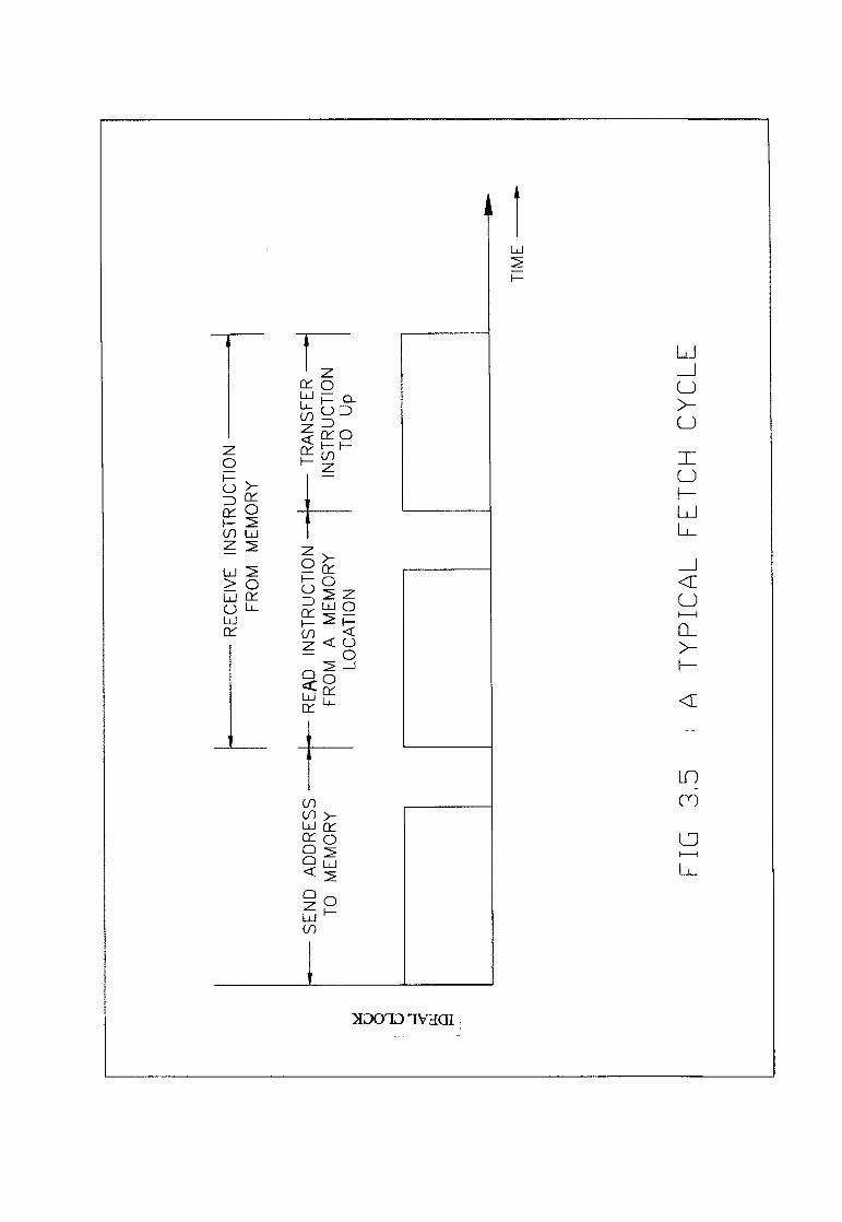
known as INSTRUCTION CYCLE. So an INSTRUCTION CYCLE is a combination of both FETCH CYCLE and EXECUTE CYCLE as shown in the figure(3.4).
FETCH CYCLE: The time taken by the microprocessor to fetch the data from the memory is known as fetch cycle, and it is
described by the following algorithm.
" beginsend the address of the next instruction to memory;receive the instruction from the memory;
end"when the fetch cycle starts the contents of the
program counter are sent to the memory.The memory responds by reading the contents of the received address and transfers them to the microprocessor. Hence one clock cycle is required to send the address, two clock cycles for reading the instruction and transfer it to the microprocessor as shown in figure(3.5). In some cases the access time of the memory may be more than two clock cycles. So the microprocessor has to wait for more than two cycles before it receives the instruction operation code.

»D01D 1V3GI
-4*
mKO
:ETC
H, E
XEC
UTE
AND
INST
RU
CTI
ON
CYC
LES
TIM
E -----
--^
1C
-FC
------
------
-----
------
-----
EC
W-^--
------
- FETC
H C
YC
LE---
----E
XEC
UTE
CYC
LE
INST
RU
CTI
ON
CYC
LE
XD0131V3CII
TIM
E
- TR
ANSF
ER
- IN
STR
UC
TIO
N
TO Up
REA
D INS
TRU
CTI
ON
FR
OM
A M
EMO
RY
LO
CAT
ION
SEN
D AD
DR
ESS
TO ME
MO
RY
RE
CE
IVE IN
STR
UC
TIO
N
FRO
M ME
MO
RY
FIG
3.5 : A
TYPI
CA
L FETC
H CY
CLE

40
EXECUTE CYCLE: The time slot to execute the instructionby the microprocessor is known as execute cycle and it may be described by the following algorithm:
"begindecode the instruction fetched; if operand in memory then fetch operand; execute instruction;
end"The fetch and execute operartions are carried out in synchronism with a clock. Serveral clock cycles elapsebefore a fetch or execute operation is performed. If the instruction contains data or address of the data, then one to two extra memory fetch cycles are needed.Figure(3.6) shows the execute cycle which is dependent of the instruction.
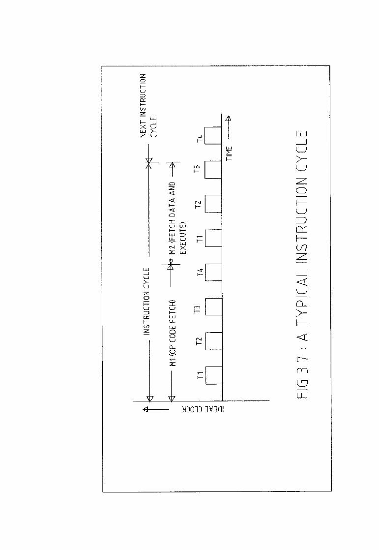
MACHINE CYCLE AND STATE: An Instruction cycle consists
of an opcode fetch cycle followed by an execute cycle. The execute cycle itself consists of zero or more fetch cycles. All these operations are performed in different time slots known as machine cycles. An instruction cycle may consist of one or more machine cycles. One machine cycle itselfconsists of several clock cycles. Each of these clock cycles is known as T-state and are referred to as T1,T2--. Figure(3.7) shows a typical instruction cycle and machine cycles within it. It shows two machine cycles Ml and M2. Ml in which the operation code is fetched and decoded consists of 4 states, M2 in which the data is fetched andexecuted consists of 3 states.

FIG
3,6 : DE
CO
DIN
G AND
EXEC
UTI
ON
TIM
E
------
------
----D
EC
OD
E AN
D EX
ECU
TE INS
TRU
CTI
ON
------
------
-----
>13013 1V3QI
FIG
3.7 :
A TYP
ICAL
INST
RU
CTI
ON
CYC
LE
-£►
TIM
E
IkT3
TZ
LI
T4
Ei
T2
Li^--
------
-- M1
{OP C
OD
E FE
TCH
} -------^ M
2 {FE
TCH
DAT
A AN
D —
dEX
ECU
TE)
NEX
T IN
STR
UC
TIO
N
CYC
LEf
INST
RU
CTI
ON
CYC
LEW
>DO~D 1V3QI
41
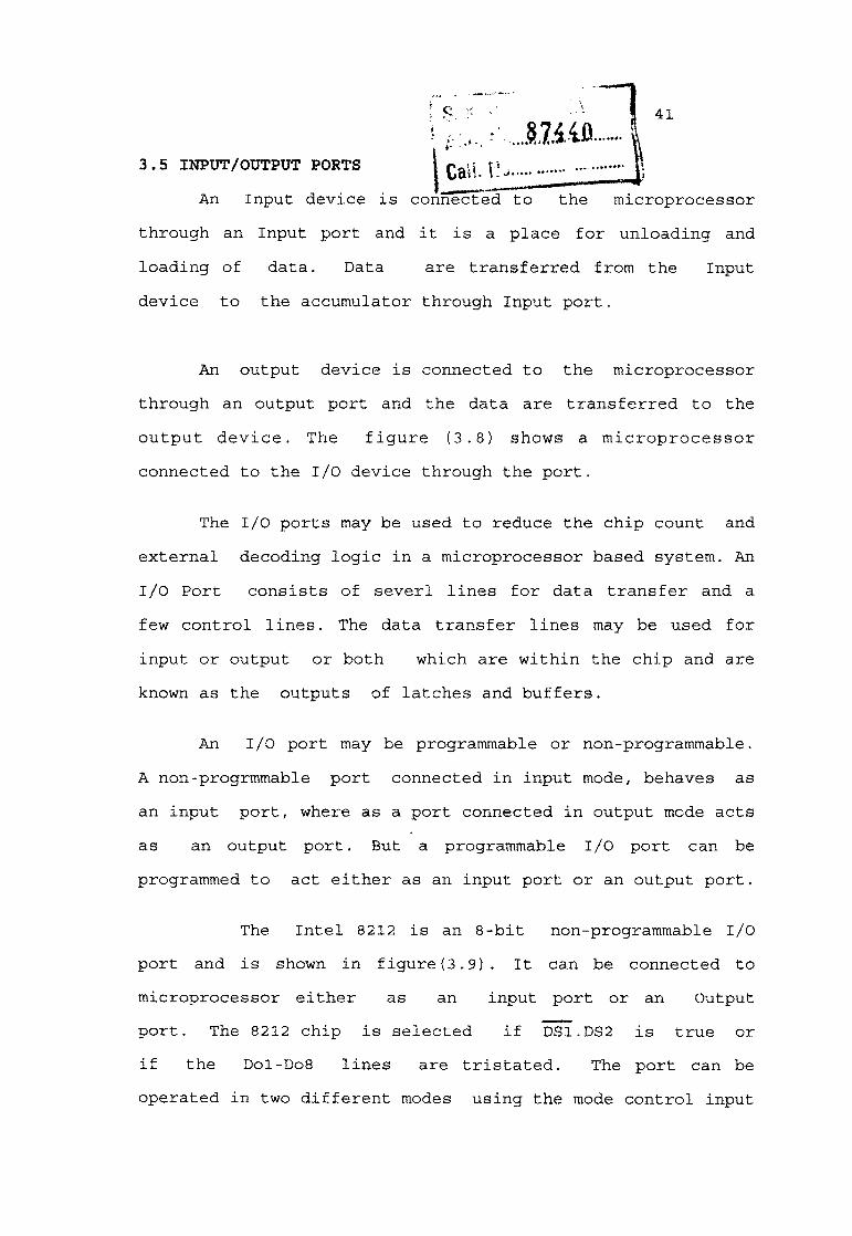
3.5 INPUT/OUTPUT PORTS | CaU. I!l..An Input device is connected to the microprocessor
through an Input port and it is a place for unloading and loading of data. Data are transferred from the Input device to the accumulator through Input port.
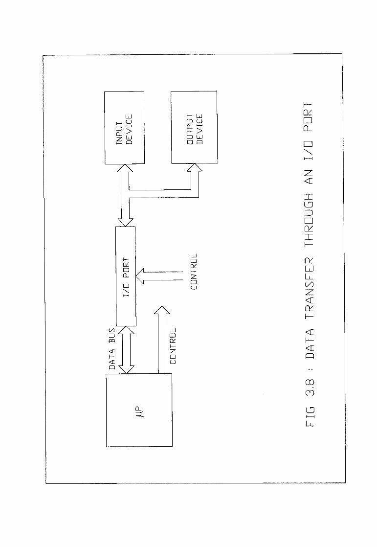
An output device is connected to the microprocessor through an output port and the data are transferred to the output device. The figure (3.8) shows a microprocessor connected to the I/O device through the port.
The I/O ports may be used to reduce the chip count and external decoding logic in a microprocessor based system. An I/O Port consists of severl lines for data transfer and a few control lines. The data transfer lines may be used for input or output or both which are within the chip and are known as the outputs of latches and buffers.
An I/O port may be programmable or non-programmable. A non-progrmmable port connected in input mode, behaves as an input port, where as a port connected in output mode acts as an output port. But a programmable I/O port can be programmed to act either as an input port or an output port.
The Intel 8212 is an 8-bit non-programmable I/O port and is shown in figure (3.9) . It can be connected to microprocessor either as an input port or an Output port. The 8212 chip is selected if DS1.DS2 is true or if the D0I-D08 lines are tristated. The port can be operated in two different modes using the mode control input
FIG
3,8 i D
ATA T
RA
NS
FER
THR
DU
GH
AN I/D
POR
T

FIG
3,9 : SC
HEM
ATI
C DIA
GR
AM
OF IN
TEL 82
12
DS
1 DS2 M
DD
E(M
D)
CLE
AR
(CLR
)
INTE
RR
UP
T(IN
T)
DA
TA □U
TPU
T(D
D1 -
DD
8)
8-B
IT I/D
PDR
T
INTE
L 8212
Vcc
G
ND
(STB
)ST
RO
BE
(Dll -
DI8
)
DA
TA INP
UT

42
(MD) . When MD is high (output mode) , the output buffers
are enabled and the input data latching occurs using the DS1.DS2 signal. When MD is low (input mode), the input data is latched using the STB signal and the output buffers are
enabled only when DS1.DS2 is true.
The port may be used to interrupt the microprocessor. The INT line goes low when the port is in the input mode and
the STB goes high. The interrupt may be cleared by a low on the CLR line. Thus if INT line is connected to an active low interrupt of a microprocessor, the latter may be interrupted after the input data has been strobed in.
programmable I/O ports : A programmable I/O port can
be programmable using IN and OUT instructions. A port may be programmable for one or more of the attributes namely(a) Simple input or output mode(b) strobed input or output mode(c) control mode.
The port may latch input data from the inputdevice or output data to the output device in the simple input or output mode, where as the data is loaded or unloaded using an external strobe signal in the strobed
mode. In the control mode, the individual pins of a port are used for controlling data transfer to or from some other
port.
3.6 PROGRAMMABLE PERIPHERAL INTERFACEA programmable peripheral interface is a multiport
device. The intel 8255A is a programmable peripheral

43
interface. It has three 8-bit ports, namely portA, portB and portC. The port 'C has been further divided into two 4-bit ports. Port C upper and port C lower. Thus a total of 4 ports are available, two 8-bit ports and two 4-bit ports. Each Port can be programmed either as an input
port or an output port.
SCHEMATIC DIAGRAM OF INTEL 8255A : Figure (3.10) shows the pin diagram of intel 8255A. It is a 40 pin I.C package, operating on a single 5V d.c supply.
CHIP SELECT (CS) : It is a chip select signal. The low status of this signal enables communication between the CPU and 8255A.
READ (RD) : When RD goes low the 8255A sends out data or status thus information to the CPU on the data bus.
WRITE(WR): When WR goes low the CPU writes data or control
word 8255A.
AO and Al: The selection of input port and control word
register is done using using AO and Al in conjuction with RD and WR. These are normally connected to the least significant bits of the address bus.
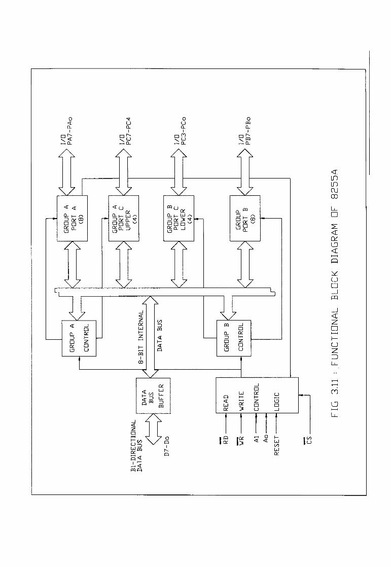
BLOCK DIAGRAM OF THE 8255A: The block diagram of Intel 8255A is shown in figure(3.11). It has two 8-bit ports ( A and B) , two 4-bit ports, (pch, pci) , the data bus buffer and control logic.

FIG
3,10 j S
CH
EMA
TIC
DIAG
RA
M DF
INTE
L 8255
_A
GN
D
vcc
PBo -
PB7
PCo -
PC3
PC
4 - PC
7
PA7
j\ T> PA
°
c
INTE
L 825
5-A
C
csR
ESE
T
Ao
A1 RD
WR
za
Do
I/O PB
7-P
Bo
I/D PC3-
PCO
I/D PC7-
PC4
I/D PA
7-P
AO
FIG
3.11 : F
UN
CTI
ON
AL BL
DC
K DIA
GR
AM
GF 82
55A
GR
DU
P
PD
RT B (8
)
k GRDUP B .
J\ PDR
T C /l
v/ LOWE
R \j
(4)
GR
DU
P A
PD
RT C
UP
PE
R
<4)
GR
DU
P A
PD
RT A
(8)
GR
DU
P B C
ON
TRO
L
c
DA
TA BU
S
REA
D
WR
ITE
CD
NTR
DL
LDG
IC
8-BI
T INTE
RN
AL
\1/
GR
DU
P A
CD
NTR
DL
DAT
AB
US
BUFF
ER
S3RD
-W
R -
A1 -
Ao
-
RES
ET-
D7-
Do
BI-D
IREC
TIO
NAL
D
ATA
BUS

44
DATA BUS: Data is transmitted or received by thebuffer upon execution of input or output instructions by the CPU. Control words and status information are
transferred through the data bus buffer.
READ/WRITE AND CONTROL LOGIC: The control section has sixlines namely RD, WR, RESET, CS, AO and Al. It accepts input from the CPU address and control buses and inturn issues commands to both of the control groups.
GROUP A AND GROUP B CONTROLS: The functionalconfiguration of each port is programmed by the system software. In essence, the CPU outputs a control word to the 8255A. The control word contains information such as MODE bit set, bit set reset etc, that initializes thefunctional configuration of the 8255A. Each of the control blocks (GroupA and GroupB) accepts commands from the Read write logic, receives CONTROL WORD from the internal data bus and issues the proper commands to its associated ports.
CONTROL GROUP A- Port A and port C upper.
CONTROL GROUP B- Port B and port C lower.The control word register can only be written
into. Read operation of the control word register is not allowed.
82 55A OPERATIONAL DESCRIPTION : The possible modecombinations by the system software is MODE 0, MODE 1 andMODE 2.

45
MODE 0 : SIMPLE INPUT OR OUTPUTThis functional configuration provides simple input and output operations for each of the three ports. No hand shaking is required. Data is simply written to or read from a specified port.The input/output features in mode 0 are as follows;
{1) outputs are latched.(2) Inputs are not latched.(3) Ports do not have handshake or interrupt capability.
MODE 1 ; INPUT OR OUTPUT WITH HAND SHAKEThis configuration provides a means for transferring I/O
data to or from a specified port in conjunction with strobes or hand shaking signals. In this mode port A and port B use the lines on port C to generate or accept hand shaking signals.
MODE 2: BIDIRECTIONAL DATA TRANSFERThis configuration is used for communicating with a peripheral device on a single 8-bit bus for both transmitting and receiving data. Hand shaking signals are provided to maintain proper bus flow discipline in a similar manner to model interrupt generation and enable/disable functions are also possible.
SINGLE BIT SET/RESET FEATURE: Any of eight bits of port C can be SET or RESET using a single out instruction.This feature reduces software requirement in control based applications. When port C is being used as status/ control for port A and port B these bits can be set or reset by using BITSET/RESET operation just as if they were data

46
output ports.
INTERRUPT CONTROL FUNCTIONS: When the 8255A is programmed to operate in mode 1 or mode 2, control signals are provided that can be used as interrupt request inputs to the CPU. The interrupt request siganls generated from port C, can be inhibited or enabled by setting or resetting the assoicated INTR flip-flop using the bit set/reset function
of port C. This function allows the programmer to disallow or allow a specific I/O device to interrupt
the CPU without affecting any other device in the interrupt
structure.
3.7 PROGRAMMABLE INTERRUPT CONTROLLERThe programmable interrupt controller is used when
several I/O devices transfer data using interrupt and they are to be connected to the same interrupt level of the microprocessor. The Intel 8259A is a single chip programmable interrupt controller. It is compatible
with 8086, 8088 and 8085 microprocessors. It is a 28pin dip I.C package and uses N-MOS technology. It requires
a single +5v supply for its operation.
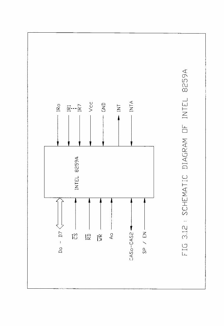
SCHEMATIC DIAGRAM OF INTEL 8259 ft:The schematic diagram of Intel 8259A is shown in
fig(3.12) Some of the details of the pins are as follows:
CS: It is a chip select signal.
WR: Write. A Low on this pin enables Intel 8259A to accept command word from CPU.
FIG
3.12 : S
CH
EMA
TIC
DIAG
RA
M DF
INTE
L 8259
A
Do -
D7 <
0
CS
—R
D —
WR
— A
o —C
AS
o-C
AS
2
SP /
EN —
Vcc
GN
D
INT
INTA
IR1 AIRo
47
RD: Read. A Low on this pin enables Intel 8259A to sendthe various status signals on the data bus for CPU.
D0-D7 : Bidirectional data bus. Control, status andinterrupt vector information are transferred via this bus.
CAS0-CAS2: Cascade lines
SP/EN: Slave program/Enable buffer.
INT: Interrupt. It is used to interrupt CPU.
INTAs Interrupt acknowledge.
IR0-IR7: Interrupt requests. I/O devices send interrupt
request through these lines.
AO: Address line. It acts in conjuction with RD, WR and CS.The Intel 8259 uses it to write a command word, to read a status and to determine the port address of the controller.
BLOCK DIAGRAM OF THE 8259A: The 8259A is upward compatible with its predecessor, the 8259 and its block diagram is as shown in figure(3.13). It includes eight blocks: control logic, Read/write logic, data bus buffer, three
registers (IRR, I SR & IMR), priority resolver and cascade buffer.
READ/WRITE LOGIC: When the address line AO is at logic 0,the controller is selected to write a command or read a status. The chip select logic and AO determine the port address of the controller.

FIG
3.13
; FUN
CTI
ON
AL BL
DC
K DIA
GR
AM
DF 82
59A
IRo
IR1
IR2
IR3
IR4
IR5
IR6
IR7
INT
INTA

48
CONTROL LOGIC: This block has two pins namely INT (Interrupt) as an output, and INTA (Interrupt acknowledge) as an input. The INT is connected to the interrupt pin of the MPU. Whenever a valid interrupt is asserted this signal goes high.
INTERRUPT REGISTERS AND PRIORITY RESOLVER: The Interrupt Request Register (IRR) has eight input lines (IR0-IR7) for interrupts. When these lines go high, the requests are stored in the register. The In-Service Register (ISR)
stores all the levels that are currently being serviced, and the Interrupt Mask Register (IMR) stores the masking bits of the interrupt lines to be masked. The Priority Resolver (PR) examines these three registers, and determines whether INT should be sent to the MPU.
CASCADE BUFFER / COMPARATOR: This block is used to extend the number of interrupt levels by cascading two or more
8259 .8259A OPERATIONAL DESCRIPTION: The 8259A should be first initialized by writing control words in the control register. The 8259A requires two types of control words:
a) Initialization command words (ICWS) andb) Operational command words (OCWS).After the 8259A is initialized, the following sequence of events occurs when one or more interrupt request lines go high.
1. The IRR stores the requests.2. The priority resolver checks three registers, the IRR ,
49
the IMR and the ISR. It resolves the priority and sets the INT high when appropriate.3. The MPU acknowledges the interrupt by sending INTA.4. After the INTA is received, the appropriate priority bit in the ISR is set to indicate which interrupt level is being served, and the corresponding bit in the IRR is reset to indicate that the request is accepted. Then, the opcode for the CALL instruction is placed on the data bus.5. When the MPU decodes the CALL instruction, it places two or more INTA signals on the data bus.6. When the 8259A receives the second INTA, it placesthe low-order byte of the CALL address on the data bus. At the third INTA, it places the high-order byte on the data bus. The CALL address is the vector memory location for the interrupt and this address is placed in thecontrol register during the initialization.7. During the third INTA pulse, the ISR bit is reseteither automatically or by a command word and this is determined by the initialization command word(IWC).8. The program sequence is transferred to the memory location specified by the CALL instruction.
3.8 PROGRAMMABLE DMA CONTROLLERDirect Memory Access(DMA) is an I/O technique commonly
used for high speed data transfer. The 8257 is aprogrammable, 4-channel, direct memory access controller. This means that four peripherals can request data transfer, and the request priorities are determinedinternally. It is a 4 0 pin I.C. package and requires a
50
single +5v supply for its operation. Four I/O devices
can be interfaced to the microprocessor through this device. It is capable of performing three operations, namely read, write and verify. During the read operation data
are directly transferred from the memory to the I/O device. During the write operation data are transferred from the I/O device to the memory. On receiving a request from I/O device, the 8257 generates sequential memory address which allows the I/O device to read or write directly
to or from the memory.
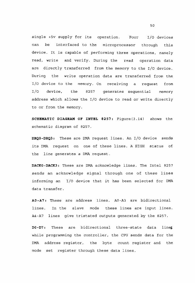
SCHEMATIC DIAGRAM OF INTEL 8257: Figure (3.14} shows theschematic diagram of 8257.
DRQ0-DRQ3: These are DMA request lines. An I/O device sends
its DMA request on one of these lines. A HIGH status of the line generates a DMA request.
DACK0-DACK3: These are DMA acknowledge lines. The Intel 8257 sends an acknowledge signal through one of these lines informing an I/O device that it has been selected for DMA
data transfer.
A0-A7: These are address lines. A0-A3 are bidirectionallines. In the slave mode these lines are input lines. A4-A7 lines give tristated outputs generated by the 8257.
D0-D7: These are bidirectional three-state data lineswhile programming the controller, the CPU sends data for the DMA address register, the byte count register and the mode set register through these data lines.
FIG
3,14
: SCH
EMA
TIC
DIAG
RA
M DF
INTE
L 8257
DR
Qo
DA
CK
o
DR
Q1
DA
CK
1
DR
Q2
DA
CK
2
DA
Q3
DA
CK
3
AEN AD
STB
TC MA
RK
7s
V <
7SS £
7 \
7^
V 7
Do-
D7
CS
CLK
RES
ET
Ao-
A3
A4-
A7
TTd
r
I/DW
REA
DY
HR
Q
HR
QA
ME
MR
ICM
W

51
ADSTB: A HIGH on this line latches the 8 MSBs of theaddress, which are sent on data bus.
I/OW: I/O write. It is a bidirectional line. In output
mode it allows the transfer of data to the I/O device during
the DMA read cycle. Data is transferred from the memory.
BLOCK DIAGRAM OP THE 8257 DMA CONTROLLER: Figure (3.15) shows the block diagram of the 8257 DMA controller. It is a programmable device which has three blocks namely data bus buffer, Read / Write logic and four channels.
DMA CHANNELS: The 8257 has four identical channels, each with two signals DRQ(DMA Request) and DACK(DMA acknowledge). Each channel has two 16-bit registers, one for the memory address where data transfer should begin, and the second for a 14- bit count. Bits D15 and D14 of the count register specify
the DMA function write, Read or verify.
SIGNAL AEN (ADDRESS ENABLE): The AEN output signal isused to disable the system data bus and control bus. This signal is necessary to switch the 8257 from the slave mode to the master mode.
DMA EXECUTION : The process of data transfer from the peripheral to the system memory under the DMA controller can be classified under two modes namely the slave mode, and master mode.
SLAVE MODE : In the slave mode the DMA controller is treated as a peripheral using the following steps:
1) The MPU selects the DMA controller through chip select.

FIG
3.15
: FUN
CTI
ON
AL BL
DC
K DIA
GR
AM OF
INTE
L 825
7DR
Q3
DAC
K3
DR
Qo
DA
CKo
DR
Q1
DA
CK
1
DR
Q2
DA
CK
2

52
2) The MPU writes the command mode and terminal count in
channel register by accessing the register through Ao-A3 and through the control signal IOR and IOW.
MASTER MODE : In master mode, the 8257 keeps checking for a DMA request, and the steps in data transfer can be as follows:
1) when the peripheral is ready for data transfer, it sends a high signal to DRQ.
2) When the DRQ has been received and the channel enabled, the control logic sets HRQ high.
3) In the next cyle, the MPU relinquishes the buses and sends the HLDA signal to the 8257.
4) After receiving the HLDA signal, the control logic
generates DACK and sends the acknowledgement to the peripheral.
5) Mean while, the 8257 enables the Signal AEN (ADDRESS ENABLES). AEN disables the MPU demultiplexed address bus A7- AO. The entire bus, A7-A0, of the 8251 becomes output.
6) The low-order byte of the memory location is placed on the A7 -AO of the 8257.
7) When the AEN signal is high, the ADSTB (address strobe) signal goes high and and places the high-order byte of the memory location on address bus A15-A8. Data transfer continues until the count reaches zero.
53
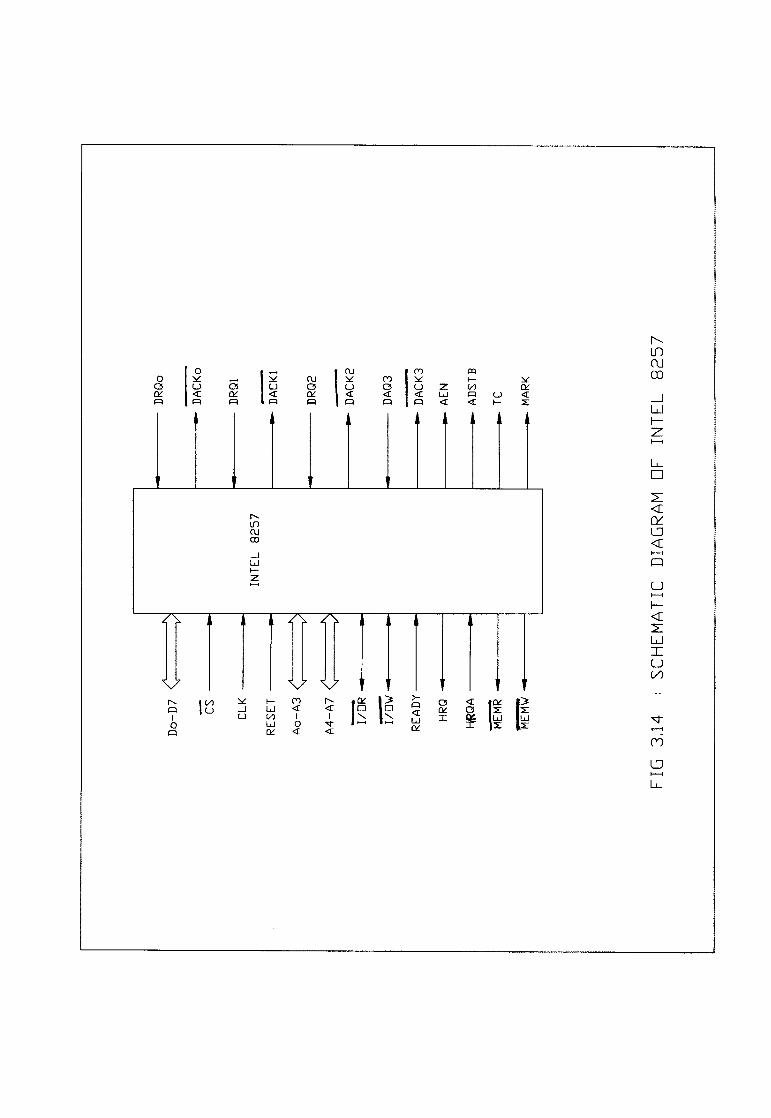
3.9 PROGRAMMABLE COMMUNICATION INTERFACEThe Programmable communications interface is used for
serial data transmission. The intel 8251A is a
Programmable communication interface. It is universal synchronous/Asynchronous Receiver/transmitter, (USART). It is
compatible with 8085, 8086, 8088, and 8748 system. The I.C chip is fabricated using N-channel silicon gate technology. The 8251A can be used to transmit/receive serial data. It
accepts data in parallel format from themicroprocessor and converts them into serial data for transmission. It also receives serial data and converts them into parallel and sends the Data in parallel format to the CPU.
SCHEMATIC DIAGRAM OF INTEL 8251A : Figure (3.16) shows a schematic diagram of intel 8251A. The description of some important pins are as follows :C/D : (control/Data) : When it is low data is transmitted onData bus. When it is high control signal are transmitted on the Data bus.
RD : (Read) . When it is low the CPU reads Data from intel
8251A.
WR : (Write) . When it is low the CPU reads data from Intel
8251A.
CTS : A low on this pin enables 8251A to transmit serial data.
TXC : (Transmitter clock) . It governs the rate of datatranmission.
SCH
EMA
TIC
DIAG
RA
M DF
INTE
L 8251
AFI
G 3,1
6
GN
D
Vcc
TXD
TXR
DY
TXE
TXC
RXD
RX
RD
Y
RXC SY
ND
ET /g
RKD
ET
INTE
L 825
1A
CS
CLK
RES
ET RD
WR c/5
"dsr
DTR
CTS
RTS
Do-
D7 <
^I

54
TXE : (Transmitter empty) . TXE goes high when 8251A has no characteristic to transmit. It indicates the end of transmission.
RXC: (Receiver clock).It governs the rate at which characters are received.
BLOCK DIAGRAM OF THE INTEL 8251A: The 8251A is the enhanced version of its predecessor, the 8251 and is compatible with the 8251. Figure(3.17) shows the block diagram of the 8251A. It has five sections namely Read/Write Control logic, Transmitter, Receiver, Data bus
Buffer, and modem control.
READ/WRITE CONTROL LOGIC AND REGISTERS: This section includes Read/Write control logic, six input signals i.e CS (chip select), C/D (control /Data), WR (write), RD (READ), RESET (reset) and CLK (CLOCK), CONTROL LOGIC, and three buffer registers namely data register, control register, and status register.
TRANSMITTER SECTION: The transmitter section converts a parallel word received from the MPU into serial bits and transmitts them over the TXD line to a peripheral. It has two registers namelya) A buffer register to hold eight bits andb) An output register to convert eight bits into a stream of serial bits.
RECEIVER SECTION: The receiver accepts serial data on the RXD line from a peripheral and converts them into parallel data. The section has two registers : the receiver input
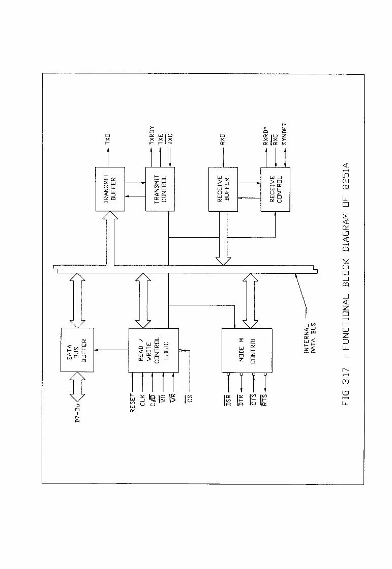
FIG
3.17
: FUN
CTI
ON
AL BL
OC
K DIA
GR
AM
OF 82
51A
RXR
DY
RXC SY
ND
ET
REC
EIVE
CO
NTR
OL
RXD
REC
EIVE
BU
FFE
R
TXR
DY
TXE
TXC
TRAN
SMIT
CO
NTR
OL
TXD
TRAN
SMIT
BUFF
ER
c
■N
INTE
RN
AL
DAT
A BU
S
MO
DE M
CO
NTR
OL
TT
REA
D /
WR
ITE
CO
NTR
OL
LOG
IC
lr
•sia-S13
• am
■ asa
res
et-
CLK
-c/
5- RD
-U
r-
cs -
D7-
Do

55
register and the buffer register.
When the RXD line goes low, the control logic assumes it as a START bit, waits for half a bit time, and samples the
line again. If the line is still low, the input register accepts the bits, forms a character, and loads it into the buffer register. Subsequently the parallel byte is transferred to the MPU when requested. In the a synchronous mode, two i/p signals and one o/p signal are
necessary i.e RXD - Receive Data, RXC - Receiver clock and RXRDY - Receiver Ready.
3.10 PROGRAMMABLE INTERVAL TIMERA programmable Counter / Interval Timer is used for
timing and counting function. Programmable interval timer
chips are Intel 8253 and 8254. The 8253 operates in the frequency range of d.c to 2.6 MHz where as 82 54 in therange of d.c to 10 MHz. Both are operated in the six modes
namely,
mode 0 : Interrupt on terminal countmode 1 : Programmable one - shotmode 2 : Rate generatormode 3 : Square wave modemode 4 : Software triggered modemode 5 : Hardware triggered mode
SCHEMATIC DIAGRAM OF INTEL 8253: The 8253 is 24-pin IC and operates at 5 V d.c. It contains threeindependent 16-bit counters. It operates under software

56
control. Figure (3.18) shows its pin diagram, some of the pins are,
a. CLKO, CLK1, and CLK2 are clocks for counter 0, counter 1 and counter 2 respectively.
b. GATEO, GATE1, and GATE2 are gate terminals,
c. OUTO, 0UT1, 0UT2 are output terminals.
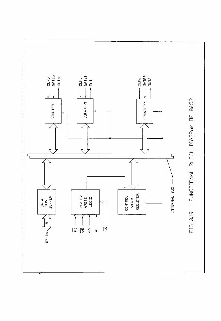
BLOCK DIAGRAM OF THE 8253: Figure (3.19) shows the blockdiagram of the 8253 . It contains three counters (0, 1 and 2) and each counter has two input signals - CLOCK (CLK) and buffer, Read/write control logic, and a control register.
DATA BUS BUFFER : It is within 8253 . It is CL 3state, bidirectional, 8 - bit buffer. It is used tointerface 8253 to the system data bus through Do - D7lines.
Read/Write control logic : The control section has fivesignals (a) RD (Read) , (b) WR (Write) (c) CS (chipselect) and the (d) Address lines AO and A1 . This control section accepts input from the system bus and thengenerates control signals for the operation of 8253.
CONTROL WORD REGISTER : This register is selected when lines AO and A1 are at logic 1. It is used to write a command word which specifies the counter to be used, its mode and either a Read or a Write operation. The control word is stored in control word Register.
OPERATIONAL DESCRIPTION OF 8253 : The 8253 containsthree independent edge triggered presettable 16 - bit

FIG
3.18
■. SC
HEM
ATI
C DIA
GR
AM
DF IN
TEL 82
53
CLK
o
GAT
Eo
□UTo
CLK
1
GAT
E1
□UT1
CLK
2
GAT
E2
□ U
T2
INTE
L 825
3
GN
D
VccWR
RDA1AoCS
Do-
D7 <
......
......
.....
)
FIG
3,19
: FUN
CTI
ON
AL BL
DC
K DIA
GR
AM
GF 82
53
CLK
P
GA
TE2
□UT2
CLK
1G
ATE
1
□UT1
CLK
oG
ATEo
OU
To

57
down counters namely, counter 0, counter 1 and counter 2. These counters are independent, and they can have
separate mode configuration and counting operation. The clock of 8253 should be less than 2.6 MHz, since the clock 0/P of 8085 is about 3 MHz.
MODE 0 ; (INTERRUPT ON TERMINAL COUNT) MODE 0 is used for the generation of accurate time delay under software control. The mode is set by loading the control word into the control word register. After mode set operation the counter is loaded by the desired count N and the counting starts if GATE is high. The counter output remains low while the counting is going on. When the cdunt reaches 0, the output becomes high and remains high until the count is reloaded or new count is loaded. If GATE is made low during counting operation counting stops.
MODE 1 : ( PROGRAMMABLE ONE - SHOT) In MODE 1 the counter acts as a retriggerable and programmable one - shot. The low to high transition of the signal applied to GATE acts as a trigger signal. When the mode is set, OUT becomes high and the counter is loaded by a count value of N.Then the counter decrements count, and the output goes low for N - clock cycles for every low to high transition of the GATE input. It goes high on the terminal count i.e counter content = 0. If the GATE input is made low to high again, the counter is reloaded by the count value N. The counter starts decrementing the count again and the output goes low for N clock pulses again. Thus one - shot mode of operation is retriggerable.

58
MODE 2 : ( RATE GENERATOR) In MODE 2 the counter acts as a simple divide by N counter. When this mode is set the output of the counter becomes high and the counter is loaded by a count of value N. For this operation GATE is kept high. In this mode the output remains high for (N- 1) clock pulses and then high again and the count N is automatically reloaded into the counter. In this way the
whole process is repeated as long as the GATE input is high .
MODE 3 : (SQUARE WAVE GENERATOR) In MODE 3 the counter acts as a square wave generator. After mode set operation the counter is loaded by a count of value N and GATE is kept high. For even values of N the output remains high for N/2 clock pulses and then goes low for next N/2
clock pulses, and the process is repeated.
MODE 4 : (SOFTWARE TRIGGERED STROBE) In mode 4 operation
the output of the counter becomes high after the mode is set and the GATE is kept high . The counter begins counting
immediately after the count is loaded in to the count register, when the counter reaches terminal count, the output goes low for one clock period, then it returns to high. The output signal may be used as strobe.
MODE 5 : (HARDWARE TRIGGERED STROBE) In this mode of operation GATE input acts as a trigger. After the mode is set, the output becomes initially high when a count value of N is loaded in to the counter. The couting begins at the first negative edge of the clock after the rising edge of the GATE input, on terminal count the output goes low for

59
one clock period, then it goes high again. As the low to high transition of the GATE input causes triggering this mode is called as hardware triggered strobe.
3.11 ANALOG SUBSYSTEMSANALOG INPUT SUBSYSTEMS: An Analog input subsystem has an ADC { Analog to Digital ) as only one of its
components.
Intel's SBC 711 Analog input Board and Burr Brown's MP20 Analog input microperipheral are two egs. These two are compatible with 8085 based systems.
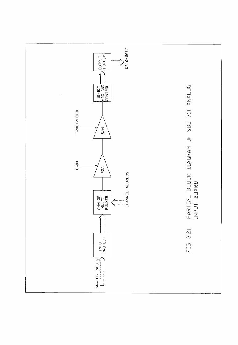
SBC 711 ANALOG INPUT BOARD: The SBC 711 is a single board device. It may be used for monitoring up to 16 process variables in a single - ended mode and up to 8 in a differential mode. It can be interfaced and addressed in a memory mapped mode. The ADC On the board gives a 12 - bit digital equivalent of the analog input on the selected input channel. Figure{3.205 shows a blcok diagram of the board.
OPERATION OF THE SBC 711 : The 16 single - ended input or 8 differential input channels are input to an analog multiplexer (MUX). By programming the MUX register any one of these input channels may be multiplexed to the programmable gain amplifier (PGA) . The PGA gain can be set to 1, 2, 4 or 8 by programing the 2 most significanat bits of the gain register.
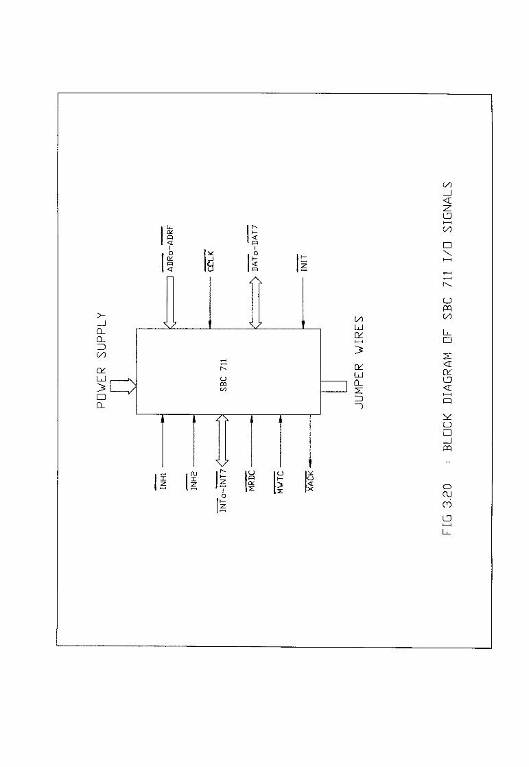
FIG
3,20
: BLO
CK D
IAG
RA
M OF
SBC
711 I/D
SIGN
ALS
JUM
PER
VIRE
S

60
The ADC provides four voltage ranges +5v, ~5v, +10v,
-lOv. Depending on the input signal voltage, a suitable gain value may be selected so that the input to the ADC,
which is the output of the PGA, lies in a suitable
range. The output of the PGA is applied to the sample and hold (S/H) amplifier and is shown in the blockdiagram of figure{3.21) SBC 711.
The latter continuously tracks the input voltage until a trigger signal is received. The trigger signal may be generated on board or from an external source or initiated by the program. When the trigger is received S/H amplifier enters the hold mode and the A/D conversion
process begins.
The output of the ADC is 12 -bit approximation of the input voltage. It may be either in straight binary code or in two's complement binary code depending on how the jumper wires have been configured. This output may be read by the processor one byte a time.
OPERATING MODES : The analog input multiplexer can be jumper programmed to operate in one of three modes random channel input, single repetitive channel input
and sequential channel input.
ANALOG OUTPUT SUBSYSTEMS : The digital output from the JJp has to be converted to a proportional analog output for driving electrical subsystems. The Digital to - Analog convertors (DACs) are used for this purpose. Intel'sSBC724 known as the Analog output Board and Burr
FIG
3.21 i P
AR
TIA
L BLD
CK
DIAG
RA
M DF
SBC 711
ANA
LDG
IN
PUT BG
AR
D
VD
AT0-
DAT
7
□UTP
UT
BUFF
ER3
12-B
IT
ADC
AND
C
ON
TRO
L
CH
ANN
EL AD
DR
ESS
ANAL
OG
S
j MULTI
PU
LXER
INP
UT
PRO
JEC
T3
ANAL
OG
INPU
TS
TRAC
K/H
OLD
GAI
N
Brown's MP10 are two egs which are compatible with Intel's 8080 and 8085 JCJps.
SBC 724 ANALOG OUTPUT BOARD: The SBC 724 consists of 4 DAC modules each capable of converting a 12 - bit input to an analog output. The output voltage range can be jumper configured to any one of the following four + I0v,
-lOv, +5v, -5v. The Up communicates with the board by means of memory write commands. The board may be assigned any base address which is a multiple of 8 by suitably connecting the jumper wires. The data sent out by the jdp is latched by the addressed DAC and the conversion begins. The latching is done when the high byte is
transferred. The low byte is initially stored in a hold register which is common to all DACs . It is transferred to the latch associated with the addressed DAC when the high byte is received.
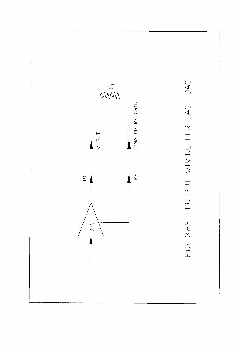
OUTPUT WIRING: The output of each DAC may be applied across a load as shown in figure (3.22) . The minimum resistance value can be detrermined from the output voltage range and the maximum output current of the DAC. Short circuit protection is provided
61
for each DAC.
FIG
3,22 :
DU
TPU
T WIR
ING
FDR
EAC
H DA
C
P2
(AN
ALD
G RE
TUR
N)
±
V-G
UT