4 low kv scanning electron microscopy - …home.ufam.edu.br/berti/nanomateriais/aulas pptx e...
TRANSCRIPT

4Low kV Scanning ElectronMicroscopy
M. David Frey
101
1. Introduction
The voltages typically associated with low-voltage scanning electron microscopyare within the range of 5 kV and lower. The low end cutoff is typically the low-est value at which a user’s microscope can achieve a usable image. The author ofthis chapter would like to see a new definition of low kV-accelerating voltagebegin within the realm of 2–1 kV. With the advent of new column designs,through the lens (TTL) secondary electron (SE) detectors and the use of electro-static lens, and similar techniques, the low end of the low kV range is typicallyreaching well below 500 V, and is often approaching 100 V. These new and triedtrue techniques are illustrated in Figs. 4.1 and 4.2. A recent development is theuse of a retarding field to modulate the landing energy of the primary electrons.By simply applying a negative potential (Vb) to the specimen, a retarding fieldcan be generated between the specimen and a grounded electrode above the spec-imen (the cold finger or the objective lens in a semi-in-lens type FEG-scanningelectron microscope [SEM] instrument). In this simple configuration, the speci-men itself is part of a “cathode lens” system. The landing energy (EL) of theincident electrons can be varied by changing the applied potential:
EL = E0 − eVb.
where E0 is the energy of the primary electron beam. The nature of the elec-tron–specimen interactions is determined by the electron landing energy EL.When eVb is equal to or larger than E0, the incident electrons will not enter thespecimen at all; in this particular configuration a mirror image may be formed.Therefore, by varying the potential applied to the sample, we can convenientlyextract useful surface information of the sample. The ultimate resolution of ultra-low voltage (ULV) SEM images is determined by the combined properties of theprobe-forming lens and the cathode lens [1]. The highest resolution secondaryimages are being obtained using TTL secondary detectors commonly referred toas TTL detectors. These TTL detectors often involve a strong magnetic field pro-jected into the chamber, or a mild electrostatic field. This field is generally used

102 M. David Frey
200 nm
MDF
Mag = 25.00 K 3
Date :5 May 2005 Aperture size = 30.00 µm
EHT = 1.00 kVWD = 3 mmESB gird = 0 V
Signal A = InlensSignal B = InlensMixing = OffMix signal = 0.0000
FIGURE 4.1. Secondary electron image of resist on Si at 1 kV uncoated.
FIGURE 4.2. Secondary electron image of resist on Si at 0.1 kV uncoated.

4. Low kV Scanning Electron Microscopy 103
to collect the low-energy SEs, which help to provide the highest resolutionimages. The type of field and detector positioning above the final lens will oftendepend upon the manufacturer of the system. Often this field type and detectorpositioning will have a great effect on image quality, as well as overall systemperformance. To further this point Joy wrote Through-the-Lens (TTL) Detectors,which use the postfield of the lens to collect the secondary signal, have not onlya much higher efficiency (DQE ~0.8), but also are more selective in the energyspectrum of the electrons that they accept. In the most advanced design the TTLdetector can, in effect, be tuned so as to collect either a pure SE signal or abackscattered signal or some mixture of the two. This provides great flexibility inimaging, and avoids the necessity of a separate BSE detector, and permitsbackscattered operation at very short working distances. The ultimate goalremains a detector that is both efficient and can be used to select any arbitraryenergy window in the emitted spectrum for imaging [2]. Low kV SEM can alsohave profound effect on the results achieved during elemental analysis. To quoteBoyes form of microscopy and microanalysis: the use of lower voltages (Boyes,1994, 1998) to generate x-ray data for elemental chemical microanalysisimproves substantially the relative sensitivity for surface layers, small particles,and light elements. The reduced cross sections for x-ray yield can be partiallycompensated with improved analysis geometries. There remains a need toachieve a critical excitation energy plus a factor of 20–40% (or overvoltage U, of1.2 < U < 1.4), and this limits analysis of complete unknowns to about 6 kV; 5kV is inadequate for the elements I, Cs, and Ba. The main light elements (B–F)and those 3d series transition metals with strong L lines are still accessible at 1.5kV and this can be especially important for the analysis of the smallest particlesand thinnest overlayers [3].
This chapter will try to address the concepts and practices of low kV SEM, andits use to attain high-resolution micrographs. (What does the term “high resolu-tion” refer to? In the case of current production SEMs, high resolution would bebetter than 2 nm.)
2. Electron Generation and Accelerating Voltage
The first thing that should be addressed is what exactly is “low kV?” To trulyunderstand the term “low kV” the reader must understand how kV is controlledor set. This will require an understanding of an “electron gun.” The basic princi-ples and design of an electron gun and an electron optical column do not varymuch from SEM to SEM. The basic design consists of a cathode and anodearrangement. Within this basic design there is an electron source. This source willnormally consist of either tungsten or lanthanum hexaboride (LaB6). The elec-trons are generated by one of a couple of methods. They are either generated ther-mally or through the use of field emission. In the case of systems wherehigh-resolution imaging is going to be done in the lower kV ranges, the user willmore than likely be using a field emission source rather than a thermal source.

In the case of the thermal emitter, the electron source is heated by running a currentresistively through a wire. As the current is increased the heating temperatureincreases. By increasing the temperature of the source, the electrons are liberateddue to lowering of the work function of the electron donor material to a pointwhere the electrons are in essence boiled off from the wire. The wire is subjectedto temperatures at or close to 2,700 K. This cloud of electrons is gathered up inthe Wehnelt cylinder. This Wehnelt cylinder contains the cathode (filament) of theelectron gun. The Wehnelt is kept slightly negative in relation to the filament,which provides a focusing effect for the cloud of electrons. The cathode is set toground potential, 0 V. The voltage of the anode is set to the voltage desired to bethe accelerating voltage (e.g., 20 or 1 kV). The anode plate contains an aperturethrough which the electrons will pass. This difference in voltage provides thepotential for acceleration of the electrons down the column [4]. This scenario iscalled thermal emission (Fig. 4.3). Normally this type of electron emission pro-vides a stable source of electrons, but is frequently associated with lower resolu-tion SEMs (an ultimate resolution of ~3 nm at 20–30 kV).
SEMs that are used at lower accelerating voltages and produce high-resolutionimages at these “low kV” settings produce their electron beam through the use ofone of the two categories of field emission. The two varieties of field emission arethermal and cold. Both have advantages and disadvantages. Generally both arevery capable for “low kV,” high-resolution imaging. The basic concept behindfield emission is an electron source that has been attached to a tungsten wire. Thiselectron source itself is a piece of tungsten. It has a tip radius smaller than 100 nm.As a negative potential is applied to the source, the small tip concentrates thispotential. This concentration of potential at the tip subjects it to a high field. Thishigh field allows the electrons to escape from the source material. The two typesof field emission guns, cold and thermal (illustrated below), function in more or
104 M. David Frey
Wehneltcylinder
Tungsten filament
Anode
FIGURE 4.3. Thermal emitter.

less the same way in respect to the field generated at the tip. If the tip is held at anegative 3–5 kV relative to the first anode, the effective electric field F at the tipis so strong (>107 V/cm) that the potential barrier for electrons becomes narrowin width as well as reduced in height by the Schottky effect. This narrow barrierallows electrons to “tunnel” directly through the barrier and leave the cathodewithout requiring any thermal energy to lift them over the work function barrier.Tungsten is the cathode material of choice since only very strong materials canwithstand the high mechanical stress placed on the tip in such a high electricalfield. A cathode current density as high as 105 A/cm2 may be obtained froma field emitter compared with about 3 A/cm2 from a tungsten hairpin filament.In a field emitter, electrons emanate from a very small virtual source (~10 nm)behind the sharp tip into a large semiangle (nearly 20˚ or about 0.3 rad), whichstill gives a high current per solid angle and thus a high brightness [5]. A secondanode is used to accelerate the electrons to the operating voltage. The only realdifferences fall into the categories of vacuum requirements are long-term sourcestability and overall I-probe (probe current) that can be generated by a source.Other considerations in regard to column design will have an effect over low kVperformance. Figure 4.4 illustrates Schottky field emission source. Table 4.1compares the different types of electron sources.
3. “Why Use Low kV”?
There are many interesting reasons why a microscopist or researcher might uselow kV. First and foremost would be charge reduction. SEM users have oftenfought the charging influences of an electron beam. Often users coat their sam-ples with a conductive coating if the samples happen to be of a nonconductive
4. Low kV Scanning Electron Microscopy 105
Surpressor
CathodeW/ZrO
CathodeW/ZrO
First anode
Second anode
Electron beamElectron trajectories
Virtualsource
FIGURE 4.4. Schottky field emission gun. (Drawing adapted from Carl Zeiss SMTLiterature.)

variety. The advantages and disadvantages of coating have long been argued andthis author does not wish to wade into this discussion. Many samples that are non-conductive often have a point where they reach equilibrium. This equilibrium isthe point where the charge into the sample equals the charge out of the sample.The charge out of the sample will be from SEs, backscattered electrons (BSE),Auger electrons, x-rays, and whatever current is absorbed and then transmittedthrough the sample to ground. This is referred to as a state of unity. Chargingcomes in several species, and often exhibits several characteristics. These speciesare either positive or negative charging. When the sample charges positively theimage will appear bright, and when there is a negative charge the image willappear dark. Charging can also be frequently seen as streaks of light or dark onan image. As the charge of a sample changes a user will often also see the imagedrift across the screen. Users frequently attribute this to stage or sample instabil-ity. These two causes can be ruled out as a cause by raising or lowering the kV. Ifthe drift either stops or changes direction, charge balance is the culprit, not stageinstability or poor sample mounting. The effect that is being seen as image driftis in fact the buildup of charge in the sample pushing the electron beam awayfrom the area to be imaged; hence the appearance of drift. If the charge on thesample becomes great enough, the result can be a reflection of the primary e-beam by the charged sample causing a scan of the chamber to result. This willhappen when the charge of the sample is greater than the charge of the primarybeam (e.g., a primary beam of 2.5 kV and a charge on the sample of 20 kV). TheSE image that is produced as a result of the excessive charge on the sample (aplastic sphere) can be seen in Fig. 4.5.
106 M. David Frey
TABLE 4.1. Electron source comparisonElectron source performance comparison
Cold field Schottky field Emitter type Thermionic Thermionic emission emission
Cathode material W LaB6 W (310) ZrO/W (100)Operating temperature (K) 2,800 1,900 300 1,800Cathode radius (nm) 60,000 10,000 ≤100 ≤1,000Effective source radius (nm) 15,000 5,000 2.5 (a) 15 (a)Emission current density (A/cm2) 3 30 17,000 5,300Total emisson current (µA) 200 80 5 200Normalized brightness (A/cm2*sr*kV) 1 × 10⁴ 1 × 10⁵ 2 × 10⁷ 1 × 10⁷
Maximum probe current 1,000 1,000 0.2 10Energy spread at the cathode (eV) 0.59 0.4 0.26 0.31Energy spread at the gun exit (eV) 1.5–2.5 1.3–2.5 0.3–0.7 0.35–0.7Beam noise (%) 1 1 10 1Emisson current drift (%/h) 0.1 0.2 5 <0.2Minimum operating vacuum (hPa) ≤1 × 10⁵ ≤1 × 10⁶ ≤1 × 10¹⁰ ≤1 × 10⁸
Cathode life (h) 200 1,000 >2,000 >2,000Cathode regeneration Not required Not required Every 6 to 8 Not requiredSensitivity to external influences Minimal Minimal High Low
Source: Adapted from Carl Zeiss SMT Literature.

The use of low kV leads to reduced beam interaction volume. It has been notedby Joy and Newbury [6] that as the energy (E0) of the incident beam is reducedthe range (R) of the electrons falls significantly (R~k.E0
1.66). This reduced inter-action volume results in the production of an SE signal from closer to the surfaceof the sample. Signal development from closer to the surface leads to more sur-face information. Low kV operation also benefits image quality of low atomicnumber (low Z) samples. At low kV the penetration depth of the electrons intolow Z materials is much less than higher kV electrons on the same samples.Frequently low Z samples will have a ghost-like or semitransparent look at higheraccelerating voltages. By lowering the kV of the beam, the resulting image willbe less transparent, and display more information about the material. Often thisreduction of interaction volume has the result of improving the resolution of x-ray microanalysis. The user must make sure that there is sufficient overvoltageto excite the peaks required for analysis of the samples of interest. It is advisableto do the analysis at higher kV settings to identify the materials present. If thespatial resolution is not satisfactory, a lowering of the accelerating voltage is rec-ommended provided that peaks for elements required for either the mapping orline scans are available. Boyes mentions that the use of low kV and high kV for
4. Low kV Scanning Electron Microscopy 107
Mag = 54 � 100 µm
LEO SUPRA 55 Signal A = SE2 EHT =2.50 kV
WD = 9 mm
FIGURE 4.5. A secondary electron image formed by charging a plastic sphere at 20 kV, andthen imaging the sample at 2.0 kV. The resulting image is formed by the low kV primarybeam being reflected about the chamber by the sample that has been charged to a higher kV.

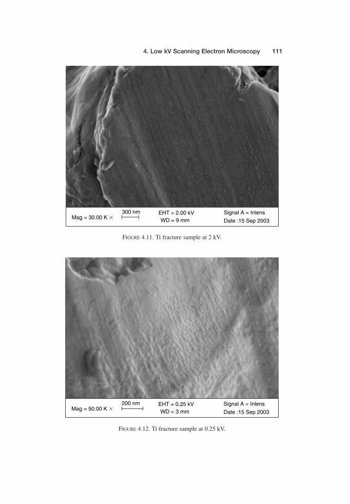
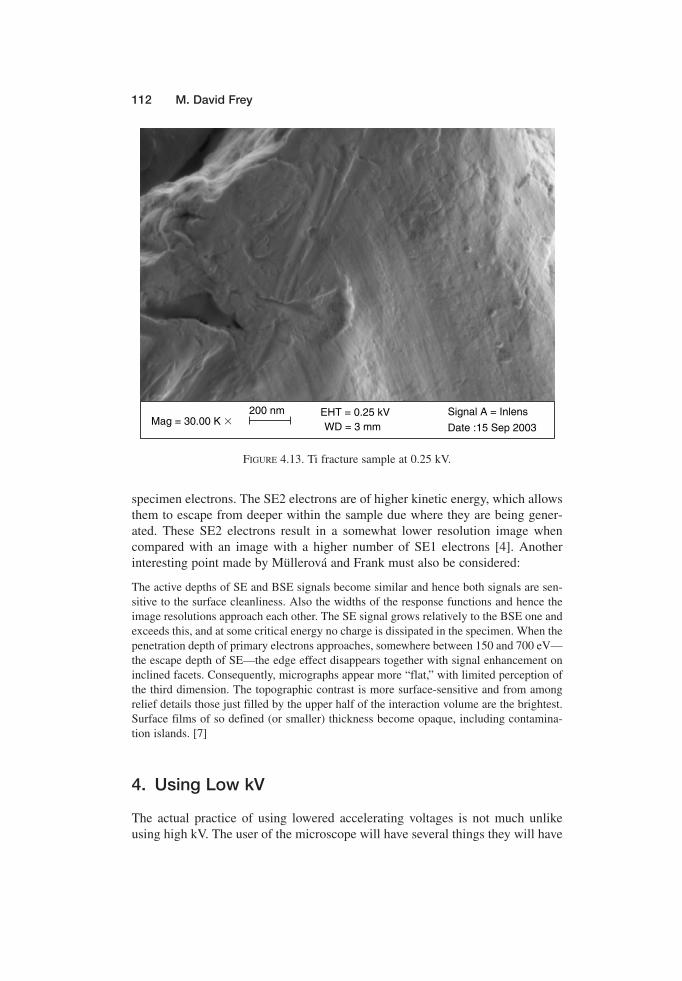
microanalysis is convergent analysis and will lead to a better understanding of the3D structure and chemistry. Figures 4.6, 4.7, 4.8, and 4.9 are SiO2 nanoparticlesand Figs. 4.10, 4.11, 4.12, and 4.13 are a Ti fracture sample. These images illus-trate how lowering the kV can reveal more surface information. This reduction ofinteraction volume also has some other effects on the signal being produced. Oneof these effects is the increase of SE emission. This increase in the emission ofSEs is the direct result of the shrinking of the interaction volume. As the interac-tion volume is brought closer to the surface, the SEs have a better opportunity toescape from the sample since they are being produced in a region where they aremore likely to escape than to be reabsorbed by the sample. It is important toremember that SEs are “defined purely on the basis of their kinetic energy; thatis, all electrons emitted from the specimen with an energy of less than 50 eV…are considered as SE.” SEs are produced as a result of the interaction of the pri-mary electron beam and electrons within the elements of the sample. This inter-action is generally a collision between a high-energy electron of the beam, and anelectron within the specimen. There is a transfer of energy from the beam elec-trons to the specimen electrons. This energy transfer results in the final energy ofthe SE that escapes from the sample. Most SEs have an energy, which is less than10 eV. SEs are of two types: SE1 and SE2 electrons. The SE1 electrons are gen-erated closer to the surface by the interaction of the primary e-beam and speci-men electrons. The SE2 electrons are generated by the interaction of BSEs and
108 M. David Frey
20 nmMag = 125.00 K � ZEISS
EHT = 20.00 kV
WD = 4 mm
Date :23 Feb 2005
Signal A = Inlens
mdf
FIGURE 4.6. SiO2 nanoparticle at 20 kV or an Al stub.

4. Low kV Scanning Electron Microscopy 109
20 nmMag = 125.00 K � ZEISS
EHT = 10.00 kV
WD = 4 mm
Date :23 Feb 2005
Signal A = Inlens
mdf
FIGURE 4.7. SiO2 nanoparticle at 10 kV or an Al stub.
20 nmMag = 125.00 K � ZEISS
EHT = 5.00 kV
WD = 4 mm
Date :23 Feb 2005
Signal A = Inlens
mdf
FIGURE 4.8. SiO2 nanoparticle at 5 kV or an Al stub.

110 M. David Frey
20 nmMag = 125.00 K � ZEISS
EHT = 1.00 kV
WD = 4 mm
Date :23 Feb 2005
Signal A = Inlens
mdf
FIGURE 4.9. SiO2 nanoparticle at 1 kV or an Al stub.
200 nmMag = 30.00 K �
EHT = 1.00 kVWD = 9 mm Date :15 Sep 2003
Signal A = Inlens
FIGURE 4.10. Ti fracture sample at 15 kV.
4. Low kV Scanning Electron Microscopy 111
300 nmMag = 30.00 K �
EHT = 2.00 kVWD = 9 mm Date :15 Sep 2003
Signal A = Inlens
FIGURE 4.11. Ti fracture sample at 2 kV.
200 nmMag = 50.00 K �
EHT = 0.25 kVWD = 3 mm Date :15 Sep 2003
Signal A = Inlens
FIGURE 4.12. Ti fracture sample at 0.25 kV.
specimen electrons. The SE2 electrons are of higher kinetic energy, which allowsthem to escape from deeper within the sample due where they are being gener-ated. These SE2 electrons result in a somewhat lower resolution image whencompared with an image with a higher number of SE1 electrons [4]. Anotherinteresting point made by Müllerová and Frank must also be considered:
The active depths of SE and BSE signals become similar and hence both signals are sen-sitive to the surface cleanliness. Also the widths of the response functions and hence theimage resolutions approach each other. The SE signal grows relatively to the BSE one andexceeds this, and at some critical energy no charge is dissipated in the specimen. When thepenetration depth of primary electrons approaches, somewhere between 150 and 700 eV—the escape depth of SE—the edge effect disappears together with signal enhancement oninclined facets. Consequently, micrographs appear more “flat,” with limited perception ofthe third dimension. The topographic contrast is more surface-sensitive and from amongrelief details those just filled by the upper half of the interaction volume are the brightest.Surface films of so defined (or smaller) thickness become opaque, including contamina-tion islands. [7]
4. Using Low kV
The actual practice of using lowered accelerating voltages is not much unlikeusing high kV. The user of the microscope will have several things they will have
112 M. David Frey
200 nmMag = 30.00 K �
EHT = 0.25 kVWD = 3 mm Date :15 Sep 2003
Signal A = Inlens
FIGURE 4.13. Ti fracture sample at 0.25 kV.

to consider. These considerations include no specific order: sample preparationand microscope preparation.
Sample preparation will include the choice of whether or not to coat the sam-ple to make it more conductive, if it is not conductive. A user will also need toconsider what type of analysis or imaging they are trying to achieve from the sys-tem. Often users will decide on a type of mounting that will accommodate thetype of sample they are evaluating. It should be thought that the sample needs tobe further processed down the line after evaluation, or is this destructive testing.Are ultra high-resolution images the goal, or are low to moderate resolutionimages acceptable for this project. Frequently, all of the questions will influencea user’s choice of mounting and preparing a sample.
To mount a sample several techniques can be offered. For high-resolutionimages a user needs to select the most mechanically stable mounting media. Thebest suggestion is to avoid any type of tape or “sticky tabs.” These will often pres-ent an image that will display a drift at high magnifications as the tabs or tape outgas in the vacuum. Often the material from which they are made rebounds after asample has been pressed into the tab or tape. They are not mechanically stable.They do provide a quick mounting solution, and are often excellent for quick anddirty microscopy when an answer is required immediately. An excellent choicefor mounting samples well is a carbon paint/dag or silver paint/paste. These typesof mounting media do take some time to dry and are not perfect for all samples,but when it comes to a rigid, stable mount they do provide a good solution as longas speed is not of the essence. There are also many different mechanical sampleholders such as vices, and spring-loaded holders that are excellent for bulk typesamples. When it comes to mounting samples such as particles, carbon nan-otubes, and liquid suspensions which can be dried down, the author has found thatcarbon-coated formvar TEM grids provide an excellent solution. They provide anice even black background without the topography often encounter with Al or Cgraphite sample stubs, by mounting the sample on a grid and by placing it into asample holder that suspends the sample. Artifacts from an SE or BSE signal beingreturned from the mounting stub will not influence the image being produced ofthe sample. The image in Fig. 4.14 is on a carbon-coated formvar TEM grid, theimage in Fig. 4.15 is on a piece of Si wafer, and the image in Fig. 4.16 is on anAl stub.
The question of coating is one that inspires a great deal of discussion. The firsttopic is whether or not to coat the sample. If the decision is made to coat the sam-ple, the next topic of discussion will often be what should be used. Often usersare restricted to the type of specimen coater they currently own. In most situationsthis coater will not always be the latest state of the art coater with all of the bellsand whistles. This fact frequently influences a user, to make the decision not tocoat their sample because of the perceived poor quality of their coater. There is arational fear of overcoating the sample, and thus obscuring the beautiful detailsthereafter at the “low kV” settings. The argument can be made that in many casesa user can flash down 1–5 s of a coating with their old out dated coater and stillget excellent high resolution results without the artifacts commonly associated
4. Low kV Scanning Electron Microscopy 113

114 M. David Frey
30 nmMag = 100.00 K �
EHT = 1.20 kVWD = 4 mmDate :23 Feb 2005
Signal A = Inlens
mdfZEISS
FIGURE 4.14. SiO2 nanoparticles on a carbon-coated formvar TEM grid mounted on anSTEM sample holder imaged at 1.2 kV.
100 nm
Mag = 100.00 K �EHT = 1.20 kV
WD = 2 mm
Date :11 Jan 2005 Cycle time = 25.1 s
Signal A = InlensSignal B = InlensSignal =1.000Mixing = Off
mdf
FIGURE 4.15. SiO2 nanoparticles on a piece of Si, imaged at 1.2 kV.

with overcoating a sample. This thin or light coating is used to stabilize thesample enough in order to take the sample from impossible to possible. I alwayssuggest a user attempt to image a sample uncoated first, and when all else failsthen coating is an apt solution. The user will still have to employ many of the strate-gies for “low kV” and “low probe current” imaging which have yet to be outlined.Most important will be the proper adjustment of their electron optical column. Thisof course varies from column to column. In the simplest set of adjustments a userwill need to adjust, focus, stigmation and aperture alignment. On more complexcolumns, user will need to contend with gun alignments, condenser lens adjust-ments, aperture alignments, biases of the samples, and other adjustments that mayinfluence the landing energy of the beam. To run a microscope at “low kV” and toproduce the best quality high-resolution images it is important to be very familiarwith the system’s controls, and the parameters that need to manipulated to producethe type of image required to tell the specimen’s story. Looking to the manufacturerfor this information is often the best place to begin.
When approaching an unknown sample, one that the user has never beforeimaged, it is a good idea to pick an arbitrary starting point. Often this is either aset of conditions where the user has had success with a similar sample, or a con-figuration where the user feels comfortable with the performance of their micro-scope. A good choice for the operation of a field emission SEM at low kV mightbe 1 kV. If the user knows that there are requirements to do x-ray analysis this
4. Low kV Scanning Electron Microscopy 115
100 nmMag = 100.00 K �
EHT = 1.00 kVWD = 2 mmDate :22 Feb 2005
Signal A = Inlens
mdfZEISS
FIGURE 4.16. SiO2 nanoparticles on an Al stub, imaged at 1.0 kV.

type of “low kV” setting might not be desired. It is always a good idea to ask ifthe sample is conductive, or nonconductive. Is it beam or charge sensitive? Thesetypes of questions will also have an effect over starting parameters. If the sampleis charge or beam sensitive a user will often need to reduce the I-probe (probe cur-rent). This will be done in most systems by changing condenser lens settings. Oncertain microscope designs changing condenser settings can be disregarded, anda smaller aperture will often be all that is needed. Once the baseline for startingconditions has been established, and the sample has been prepared and insertedinto the microscope, the user can begin to work out the best conditions for imag-ing the sample. This is a relatively unglamorous process, one that amounts to trialand error. Beginning with the baseline settings it is good to decide whether or notto increase or decrease the kV setting in response to a less than perfect image.Once this decision has been made the user can experiment with the kV settingsuntil the state of equilibrium has been reached. This experimentation amounts tochanging the kV, and observing the response of the sample. If there is more charg-ing of the sample as a result of the choice to increase or decrease the kV settingthe user should reverse course, and find a point that is halfway between the start-ing point, and the last adjustment. If his adjustment does not yield better resultsthen the user may consider going to a point that is greater or less than the start-ing point by the amount adjusted (e.g., 1, 0.5, 0.75, and 1.5 kV). If the chargeappears to be negative, then an increase in kV is what is required, and if thecharge appears to be positive, then a reduction in kV is the answer. Often verysmall difference in kV can result in a charge balance being reached. A goodexample is shown in Figs. 4.17 and 4.18. These images are of uncoated latexspheres. The difference in kV is 390 V. This point of charge equilibrium wasfound by stepping through the kV range in 10 V steps until the charge is dissi-pated. Frequently this trial and error will be a cycle that will eventually result ina charge balance on the sample. Sometime a reduction in I-probe will also berequired once the equilibrium has been reached. If it is hard to find this point ofequilibrium, coating may be the answer to imaging the sample provided that it isan option. Figures 4.19 and 4.20 illustrate how a small amount of coating canimprove the image significantly without influencing the sample. One of the otherparameters that often influences the sample charge balance and must be consid-ered is the dwell time of the beam on the sample. Dwell time will often have aneffect on the charge balance of the sample. The shorter the dwell time the betterfor samples which is nonconductive, or suffer from poor conductivity. A draw-back to a shorter dwell time is a reduction in the signal produced by the interac-tion of the beam with the sample. When deceasing the dwell time leads to animage considered unusable to illustrate the characteristics of the sample a userwill need to find an appropriate method to improve the image being produced.Normally this will require the use of features specific to the microscope in use.Many systems have the ability to do noise reduction. This is when the image isfiltered through the use of averaging to remove the noise that results from thelowered signal production.
116 M. David Frey

4. Low kV Scanning Electron Microscopy 117
Mag = 950 �10 µm
LEO SUPRA 55 Signal A = Inlens EHT =1.47 kV
WD = 2 mm
FIGURE 4.17. Uncoated latex spheres at 1.47 kV.
Mag = 950 �10 µm
LEO SUPRA 55 Signal A = Inlens EHT =1.08 kV
WD = 2 mm
FIGURE 4.18. Uncoated latex spheres at 1.08 kV. A difference of 390 V.

118 M. David Frey
200 nm Mag = 25.00 K �Cycle time = 12.8 s ZEISS
EHT = 0.25 kVWD = 3 mmMixing = OffDate :31 Mar 2005
Signal A = InlensSignal B = InlensSignal =1.000
mdf
FIGURE 4.19. Uncoated filter sample at 0.25 kV.
200 nm Mag = 25.00 K � Cycle time = 25.1 s ZEISS
EHT = 1.00 kVWD = 3 mmMixing = OffDate :31 Mar 2005
Signal A = InlensSignal B = InlensSignal =1.000
mdf
FIGURE 4.20. Filter sample coated for 5 s with Pt/Pd, imaged at 1 kV.

5. Conclusion
Low kV is not a realm where users should fear to tread. It is a gateway to the rev-elation of new and interesting features. It will help users discover new propertiesof their nanomaterials, which have been hidden by the overpowering of high kV,high beam penetration, and high-resolution SEM. Dr. Oliver Wells in theMay/June 2002 Microscopy Today wrote about Jack Ramsey’s principle, “Thereis no best way of doing anything” [8]. This is a very fair statement, and one thatis very accurate when it comes to the idea of performing scanning electronmicroscopy at low kV. Low kV is not always the answer to the best possible imag-ing of every sample. Samples often give the user clues as to where to go for thebest imaging and analytical conditions. Users need to keep their eyes open forthese clues, take the time to investigate the sample, and be very familiar with thecontrols and performance of their particular SEM. This familiarity with their sys-tem will allow them to exploit relationships of electron microscopy so as to pro-duce the results that will best tell the story of their samples and research. After allthe SEM is a tool for making the invisible, visible. Without the skills and under-standing of the relationships the results will not help to elucidate the hiddenworld.
References1. E. D. Boyes, Microsc. Microanal., 6 (2000) 307.2. J. Goldstein, D. E. Newbury, D. C. Joy, et al., Scanning Electron Microscopy and X-Ray
Microanalysis, 3rd edition, Kluwer Academic/Plenum Publishers, New York (2003).3. J. Y. Liu, Microsc. Microanal., 8(Suppl. 2) (2002).4. D. C. Joy, Microsc. Microanal., 8(Suppl. 2) (2002).5. J. Goldstein, D. E. Newbury, D. C. Joy, et al., Scanning Electron Microscopy and X-ray
Microanalysis, 3rd edition, Kluwer Academic/Plenum Publishers, New York (2003).Supplemental CD.
6. D. C. Joy and D. Newbury, Low voltage scanning electron microscopy, Microsc. Today,10(2) (2002).
7. I. Müllerová and L. Frank, Contrast mechanisms in the scanning low energy electronmicroscopy, Microsc. Microanal., 9(Suppl. 3), Microscopy Society of America (2003).
8. W. C. Oliver, Low voltage scanning electron microscopy, Microsc. Today, 10(3) (2002).
4. Low kV Scanning Electron Microscopy 119