4-wire interfaced, 7-, 14-, and 16-segment alpha- …max6850 4-wire interfaced, 7-, 14-, and...
TRANSCRIPT

General DescriptionThe MAX6850 compact vacuum-fluorescent display(VFD) controller provides microprocessors with the mul-tiplex timing for 7-segment, 14-segment, or 16-segmentalphanumeric VFD displays up to 96 characters andcontrols industry-standard, shift-register, high-voltagegrid/anode VFD tube drivers. The device supports dis-play tubes using either one or two digits per grid, aswell as universal displays. Hardware is included to sim-plify the generation of cathode bias and filament sup-plies and to provide up to five logic outputs, including abuzzer driver. The MAX6850 provides an internal cross-point switch to match any tube-driver shift-registergrid/anode order, and is compatible with both chip-in-glass and external tube drivers.The MAX6850 includes an ASCII 104-character font,multiplex scan circuitry, and static RAM that storesdigit, cursor, and annunciator data, as well as font datafor 24 user-definable characters. The display intensitycan be adjusted by an internal 16-step digital bright-ness control. The device also includes separate annun-ciator and cursor control with automatic blinking, aswell as a low-power shutdown mode.The MAX6850 provides timing to generate the PWMwaveforms to drive the tube filament from a DC supply.The filament drive is synchronized to the display multi-plexing to eliminate beat artifacts. The MAX6850 iscompatible with SPI™ and QSPI™.For a 2-wire interfaced version, refer to the MAX6851*data sheet.
Applications
Features High-Speed 26MHz SPI-/QSPI-/MICROWIRE™-
Compatible Serial Interface
2.7V to 3.6V Operation
Controls Up to 48 Grids of 7-Segment, 14-Segment,or 16-Segment Alphanumeric Digits
One Digit and Two Digits per Grid and UniversalDisplays Supported
16-Step Digital Brightness Control
Built-In ASCII 104-Character Font
24 User-Definable Characters
Up to Four Annunciators per Grid with AutomaticBlinking Control
Separate Cursor Control with Automatic Blinking
Filament Drive Full-Bridge Waveform Synthesis
Buzzer Tone Generator with Single-Ended orPush-Pull Driver
Up to Five General-Purpose Logic Outputs
9µA Low-Power Shutdown (Data Retained)
16-Pin QSOP Package
MA
X6
85
0
4-Wire Interfaced, 7-, 14-, and 16-Segment Alpha-numeric Vacuum-Fluorescent Display Controller
________________________________________________________________ Maxim Integrated Products 1
Ordering Information
19-2635; Rev 1; 1/03
For pricing, delivery, and ordering information, please contact Maxim/Dallas Direct! at 1-888-629-4642, or visit Maxim’s website at www.maxim-ic.com.
PART TEMP RANGE PIN-PACKAGE
MAX6850AEE -40°C to +125°C 16 QSOP
Display Modules
Retail POS Displays
Weight and TareDisplays
Bar Graph Displays
Industrial Controllers
White Goods
Professional AudioEquipment
SPI and QSPI are trademarks of Motorola, Inc.
MICROWIRE is a trademark of National Semiconductor Corp.
*Future product—contact factory for availability.
MAX6850VFCLK
VFDOUT
VFLOAD
VFBLANK
OSC2
DIN
SCLK
OSC1
CS
DOUT
SCLK
CS
MICROCONTROLLER
56pF
0.1µF
GND
CHIP-ON-GLASS VFD
VFD SUPPLY VOLTAGE
10kΩ
Typical Application Circuit
Pin Configuration and Functional Diagram appear at end ofdata sheet.

MA
X6
85
0
4-Wire Interfaced, 7-, 14-, and 16-Segment Alpha-numeric Vacuum-Fluorescent Display Controller
2 _______________________________________________________________________________________
ABSOLUTE MAXIMUM RATINGS
Stresses beyond those listed under “Absolute Maximum Ratings” may cause permanent damage to the device. These are stress ratings only, and functionaloperation of the device at these or any other conditions beyond those indicated in the operational sections of the specifications is not implied. Exposure toabsolute maximum rating conditions for extended periods may affect device reliability.
Voltage (with respect to GND)V+ .............................................................................-0.3V to +4VDIN, SCLK, CS ......................................................-0.3V to +5.5VAll Other Pins................................................-0.3V to (V+ + 0.3V)Current
V+..................................................................................200mAGND.............................................................................-200mAPHASE1, PHASE2, PORT0, PORT1, PUMP................±150mAVFCLK, VFDOUT, VFLOAD, VFBLANK ......................±150mA
Continuous Power Dissipation (TA = +70°C)16-Pin QSOP (derate at 8.34mW/°C above +70°C).....667mW
Operating Temperature Range (TMIN, TMAX)MAX6850AEE................................................-40°C to +125°C
Junction Temperature ......................................................+150°CStorage Temperature Range .............................-65°C to +150°CLead Temperature (soldering, 10s) .................................+300°C
DC ELECTRICAL CHARACTERISTICS(Typical operating circuit, V+ = 2.7V to 3.6V, TA = TMIN to TMAX, unless otherwise noted.) (Note 1)
PARAMETER SYMBOL CONDITIONS MIN TYP MAX UNITS
Operating Supply Voltage V+ 2.7 3.6 V
TA = TMIN toTMAX
85Shutdown Supply Current ISHDN
Shutdown mode, all digitalinputs at V+ or GND
TA = +25°C 9 30
µA
TA = TMIN toTMAX
3.5Operating Supply Current I+
OSC = 4MHzVFLOAD, VFDOUT, VFCLK,VFBLANK, loaded 100pF TA = +25°C 1.7 3.0
mA
Master Clock Frequency (OSCInternal Oscillator)
fOSC
OSC1 fitted with COSC = 56pF, OSC2 fittedwith ROSC = 10kΩ; see the TypicalOperating Circuit
4 MHz
Master Clock Frequency (OSCExternal Oscillator)
OSC1 overdriven with external fOSC 2 8 MHz
Dead-Clock ProtectionFrequency
200 kHz
OSC High Time tCH 50 ns
OSC Low Time tCL 50 ns
Fast or Slow Segment Blink DutyCycle
(Note 2) 49.5 50.5 %
LOGIC INPUTS AND OUTPUTS
Input Leakage Current DIN,SCLK, CS
IIH, IIL 0.2 1 µA
Logic-High Input Voltage DIN,SCLK, CS
VIH 2.4 V
Logic-Low Input Voltage DIN,SCLK, CS
VIL 0.6 V

MA
X6
85
0
4-Wire Interfaced, 7-, 14-, and 16-Segment Alpha-numeric Vacuum-Fluorescent Display Controller
_______________________________________________________________________________________ 3
PARAMETER SYMBOL CONDITIONS MIN TYP MAX UNITS
Output Rise and Fall TimePHASE1, PHASE2, PORT0,PORT1, PUMP, VFLOAD,VFDOUT, VFCLK, VFBLANK
tRFT CLOAD = 100pF 25 ns
Output High-VoltagePHASE1, PHASE2, PORT0,PORT1, PUMP, VFLOAD,VFDOUT, VFCLK, VFBLANK
VOH ISOURCE = 10 mA V + - 0.6 V
Output Low-VoltagePHASE1, PHASE2, PORT0,PORT1, PUMP, VFLOAD,VFDOUT, VFCLK, VFBLANK
VOL ISINK = 10 mA 0.4 V
Output Short-Circuit SourceCurrent PHASE1, PHASE2,PORT0, PORT1, PUMP, VFLOAD,VFDOUT, VFCLK, VFBLANK
IOHSCOutput programmed high, output shortcircuit to GND (Note 2)
62 125 mA
Output Short-Circuit Sink CurrentPHASE1, PHASE2, PORT0,PORT1, PUMP, VFLOAD,VFDOUT, VFCLK, VFBLANK
IOLSCOutput programmed low, output shortcircuit to V+ (Note 2)
72 125 mA
4-WIRE SERIAL INTERFACE TIMING CHARACTERISTICS (Figure 8)
SCLK Clock Period tCP 38.4 ns
SCLK Pulse Width High tCH 19 ns
SCLK Pulse Width Low tCL 19 ns
CS Fall to SCLK Rise Setup Time tCSS 9.5 ns
SCLK Rise to CS Rise Hold Time tCSH 5 ns
DIN Setup Time tDS 9.5 ns
DIN Hold Time tDH 2 ns
Minimum CS Pulse High tCSW 19 ns
DOUT Cascade Setup TimePORT0, PORT1
tCSU PORT0 and/or PORT1 enabled as DOUT 9.5 ns
VFD INTERFACE TIMING CHARACTERISTICS (Figure 11)
VFCLK Clock Period tVCP (Note 2) 500 2050 ns
VFCLK Pulse Width High tVCH (Note 2) 250 ns
VFCLK Pulse Width Low tVCL (Note 2) 250 ns
VFCLK Rise to VFD Load RiseHold Time
tVCSH (Note 2) 19 µs
VFDOUT Setup Time tVDS (Note 2) 50 ns
VFLOAD Pulse High tVCSW (Note 2) 245 ns
Note 1: All parameters tested at TA = +25°C. Specifications over temperature are guaranteed by design.Note 2: Guaranteed by design.
DC ELECTRICAL CHARACTERISTICS (continued)(Typical operating circuit, V+ = 2.7V to 3.6V, TA = TMIN to TMAX, unless otherwise noted.) (Note 1)
MA
X6
85
0
4-Wire Interfaced, 7-, 14-, and 16-Segment Alpha-numeric Vacuum-Fluorescent Display Controller
4 _______________________________________________________________________________________
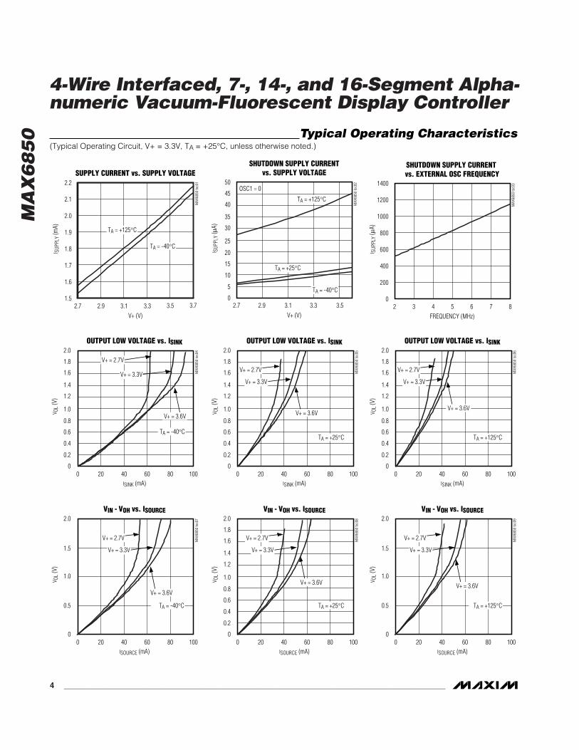
Typical Operating Characteristics(Typical Operating Circuit, V+ = 3.3V, TA = +25°C, unless otherwise noted.)
SUPPLY CURRENT vs. SUPPLY VOLTAGE
MAX
6850
toc0
1
V+ (V)
I SUP
PLY
(mA)
3.53.33.12.9
1.6
1.7
1.8
1.9
2.0
2.1
2.2
1.52.7 3.7
TA = -40°C
TA = +125°C
SHUTDOWN SUPPLY CURRENT vs. SUPPLY VOLTAGE
MAX
6850
toc0
2
V+ (V)
I SUP
PLY
(µA)
3.53.33.12.9
5
15
20
35
40
45
50
02.7
TA = -40°C
TA = +25°C
TA = +125°C
10
25
30
OSC1 = 0
FREQUENCY (MHz)76543
200
400
600
800
1000
1200
1400
02 8
SHUTDOWN SUPPLY CURRENT vs. EXTERNAL OSC FREQUENCY
MAX
6850
toc0
3
I SUP
PLY
(µA)
806040200 100
OUTPUT LOW VOLTAGE vs. ISINK
MAX
6850
toc0
4
ISINK (mA)
V OL (
V)
0.2
0.6
0.8
1.4
1.6
1.8
2.0
0
TA = -40°C
0.4
1.0
1.2
V+ = 3.3V
V+ = 3.6V
V+ = 2.7V
806040200 100
OUTPUT LOW VOLTAGE vs. ISINK
MAX
6850
toc0
5
ISINK (mA)
V OL (
V)
0.2
0.6
0.8
1.4
1.6
1.8
2.0
0
TA = +25°C0.4
1.0
1.2
V+ = 3.6V
V+ = 2.7V
V+ = 3.3V
806040200 100
OUTPUT LOW VOLTAGE vs. ISINK
MAX
6850
toc0
6
ISINK (mA)
V OL (
V)
0.2
0.6
0.8
1.4
1.6
1.8
2.0
0
TA = +125°C0.4
1.0
1.2
V+ = 3.6V
V+ = 2.7V
V+ = 3.3V
806040200 100
VIN - VOH vs. ISOURCE
MAX
6850
toc0
7
ISOURCE (mA)
V OL (
V)
0.5
1.5
2.0
0
1.0
TA = -40°C
V+ = 3.6V
V+ = 2.7V
V+ = 3.3V
806040200 100
VIN - VOH vs. ISOURCE
MAX
6850
toc0
8
ISOURCE (mA)
V OL (
V)
0.2
0.6
0.8
1.4
1.6
1.8
2.0
0
TA = +25°C0.4
1.0
1.2
V+ = 3.6V
V+ = 2.7V
V+ = 3.3V
806040200 100
VIN - VOH vs. ISOURCEM
AX68
50 to
c09
ISOURCE (mA)
V OL (
V)
0.5
1.5
2.0
0
1.0
TA = +125°C
V+ = 3.6V
V+ = 2.7V
V+ = 3.3V
MA
X6
85
0
4-Wire Interfaced, 7-, 14-, and 16-Segment Alpha-numeric Vacuum-Fluorescent Display Controller
_______________________________________________________________________________________ 5
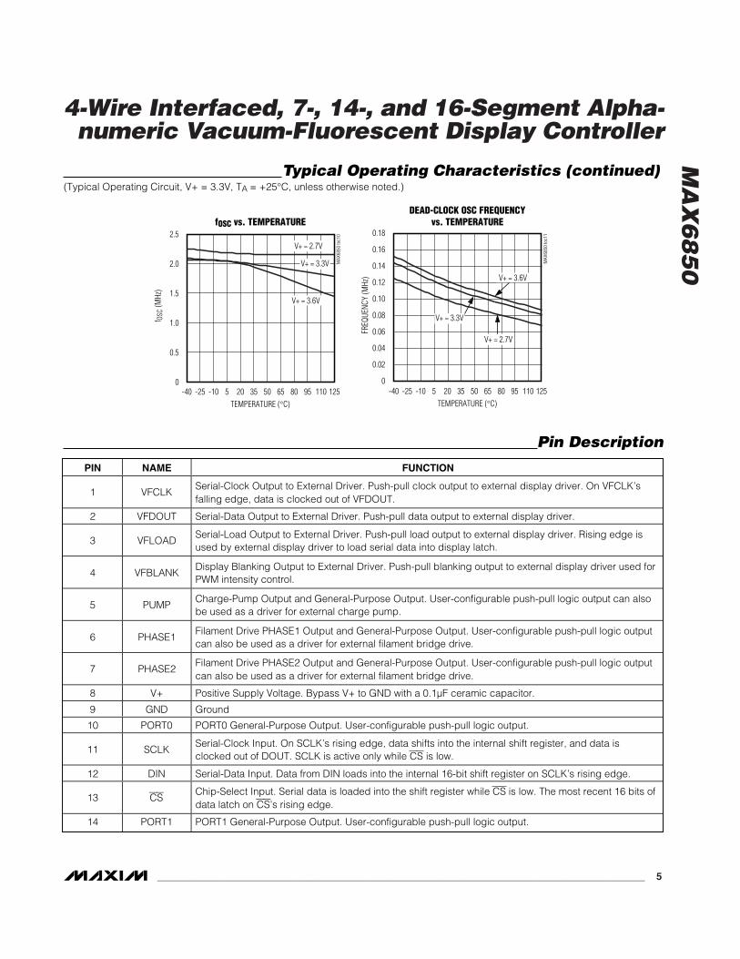
fOSC vs. TEMPERATURE
MAX
6850
toc1
0
TEMPERATURE (°C)
f OSC
(MHz
)
1109580655035205-10-25
0.5
1.0
1.5
2.0
2.5
0-40 125
V+ = 2.7V
V+ = 3.3V
V+ = 3.6V
DEAD-CLOCK OSC FREQUENCYvs. TEMPERATURE
MAX
6850
toc1
1
TEMPERATURE (°C)
FREQ
UENC
Y (M
Hz)
1109580655035205-10-25-40 125
0.02
0.04
0.06
0.08
0.10
0.12
0.14
0.16
0.18
0
V+ = 2.7V
V+ = 3.6V
V+ = 3.3V
Typical Operating Characteristics (continued)(Typical Operating Circuit, V+ = 3.3V, TA = +25°C, unless otherwise noted.)
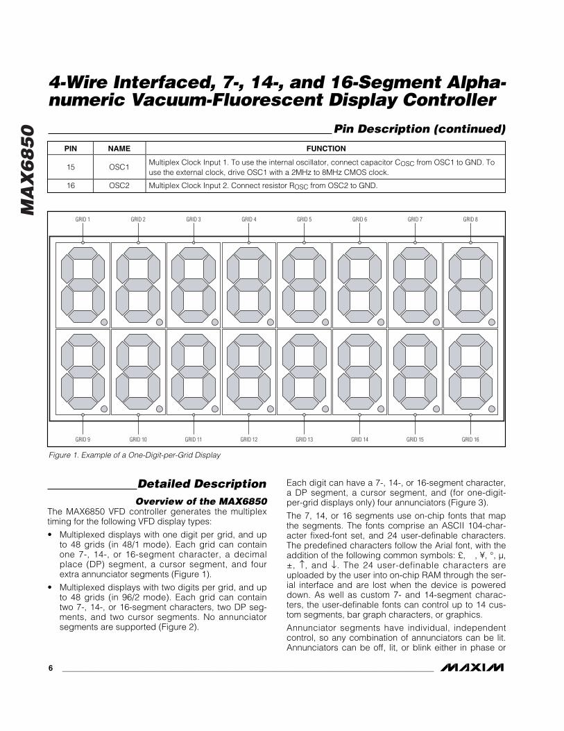
Pin Description
PIN NAME FUNCTION
1 VFCLKSerial-Clock Output to External Driver. Push-pull clock output to external display driver. On VFCLK’sfalling edge, data is clocked out of VFDOUT.
2 VFDOUT Serial-Data Output to External Driver. Push-pull data output to external display driver.
3 VFLOADSerial-Load Output to External Driver. Push-pull load output to external display driver. Rising edge isused by external display driver to load serial data into display latch.
4 VFBLANKDisplay Blanking Output to External Driver. Push-pull blanking output to external display driver used forPWM intensity control.
5 PUMPCharge-Pump Output and General-Purpose Output. User-configurable push-pull logic output can alsobe used as a driver for external charge pump.
6 PHASE1Filament Drive PHASE1 Output and General-Purpose Output. User-configurable push-pull logic outputcan also be used as a driver for external filament bridge drive.
7 PHASE2Filament Drive PHASE2 Output and General-Purpose Output. User-configurable push-pull logic outputcan also be used as a driver for external filament bridge drive.
8 V+ Positive Supply Voltage. Bypass V+ to GND with a 0.1µF ceramic capacitor.
9 GND Ground
10 PORT0 PORT0 General-Purpose Output. User-configurable push-pull logic output.
11 SCLKSerial-Clock Input. On SCLK’s rising edge, data shifts into the internal shift register, and data isclocked out of DOUT. SCLK is active only while CS is low.
12 DIN Serial-Data Input. Data from DIN loads into the internal 16-bit shift register on SCLK’s rising edge.
13 CSChip-Select Input. Serial data is loaded into the shift register while CS is low. The most recent 16 bits ofdata latch on CS’s rising edge.
14 PORT1 PORT1 General-Purpose Output. User-configurable push-pull logic output.
MA
X6
85
0
Detailed DescriptionOverview of the MAX6850
The MAX6850 VFD controller generates the multiplextiming for the following VFD display types:
• Multiplexed displays with one digit per grid, and upto 48 grids (in 48/1 mode). Each grid can containone 7-, 14-, or 16-segment character, a decimalplace (DP) segment, a cursor segment, and fourextra annunciator segments (Figure 1).
• Multiplexed displays with two digits per grid, and upto 48 grids (in 96/2 mode). Each grid can containtwo 7-, 14-, or 16-segment characters, two DP seg-ments, and two cursor segments. No annunciatorsegments are supported (Figure 2).
Each digit can have a 7-, 14-, or 16-segment character,a DP segment, a cursor segment, and (for one-digit-per-grid displays only) four annunciators (Figure 3).
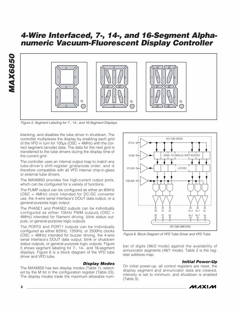
The 7, 14, or 16 segments use on-chip fonts that mapthe segments. The fonts comprise an ASCII 104-char-acter fixed-font set, and 24 user-definable characters.The predefined characters follow the Arial font, with theaddition of the following common symbols: £, , ¥, °, µ,±, ↑, and ↓. The 24 user-definable characters areuploaded by the user into on-chip RAM through the ser-ial interface and are lost when the device is powereddown. As well as custom 7- and 14-segment charac-ters, the user-definable fonts can control up to 14 cus-tom segments, bar graph characters, or graphics.
Annunciator segments have individual, independentcontrol, so any combination of annunciators can be lit.Annunciators can be off, lit, or blink either in phase or
4-Wire Interfaced, 7-, 14-, and 16-Segment Alpha-numeric Vacuum-Fluorescent Display Controller
6 _______________________________________________________________________________________
PIN NAME FUNCTION
15 OSC1Multiplex Clock Input 1. To use the internal oscillator, connect capacitor COSC from OSC1 to GND. Touse the external clock, drive OSC1 with a 2MHz to 8MHz CMOS clock.
16 OSC2 Multiplex Clock Input 2. Connect resistor ROSC from OSC2 to GND.
Pin Description (continued)
GRID 1 GRID 2 GRID 3 GRID 4 GRID 5 GRID 6 GRID 7 GRID 8
GRID 9 GRID 10 GRID 11 GRID 12 GRID 13 GRID 14 GRID 15 GRID 16
Figure 1. Example of a One-Digit-per-Grid Display
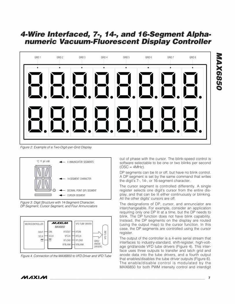
out of phase with the cursor. The blink-speed control issoftware selectable to be one or two blinks per second(OSC = 4MHz).
DP segments can be lit or off, but have no blink control.A DP segment is set by the same command that writesthe digit’s 7-, 14-, or 16-segment character.
The cursor segment is controlled differently. A singleregister selects one digit’s cursor from the entire dis-play, and that can be lit either continuously or blinking.All the other digits’ cursors are off.
The designations of DP, cursor, and annunciator areinterchangeable. For example, consider an applicationrequiring only one DP lit at a time, but the DP needs toblink. The DP function does not have blink capability.Instead, the DP segments on the display are routed(using the output map) to the cursor function. In thiscase, the DP segments are controlled using the cursorregister.
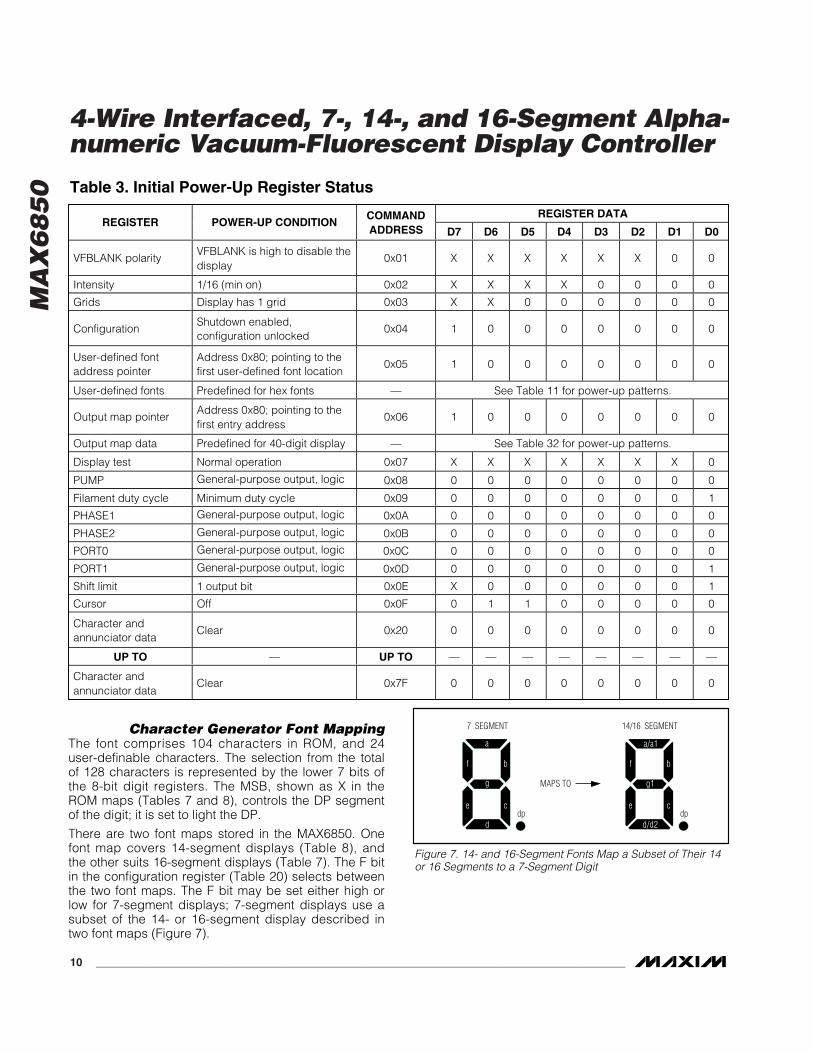
The output of the controller is a 4-wire serial stream thatinterfaces to industry-standard, shift-register, high-volt-age grid/anode VFD tube drivers (Figure 4). This inter-face uses three outputs to transfer and latch grid andanode data into the tube drivers, and a fourth outputthat enables/disables the tube driver outputs (Figure 6).The enable/disable control is modulated by theMAX6850 for both PWM intensity control and interdigit
MA
X6
85
0
4-Wire Interfaced, 7-, 14-, and 16-Segment Alpha-numeric Vacuum-Fluorescent Display Controller
_______________________________________________________________________________________ 7
GRID 1 GRID 2 GRID 3 GRID 4 GRID 5 GRID 6 GRID 7 GRID 8
Figure 2. Example of a Two-Digit-per-Grid Display
°C °F pH mW 4 ANNUNCIATOR SEGMENTS
14-SEGMENT CHARACTER
CURSOR SEGMENT
DECIMAL POINT (DP) SEGMENT
Figure 3. Digit Structure with 14-Segment Character, DP Segment, Cursor Segment, and Four Annunciators
MAX6850
VFCLK
VFDOUT
VFLOAD
DIN
SCLK
VFBLANK
VFDIN
VFCLK
VFLOAD
VFBLANK
MICROCONTROLLER VFD TUBE DRIVER
CS
DOUT
SCLK
CS
VFD
TUBE
GRID/ANODEDRIVERS
Figure 4. Connection of the MAX6850 to VFD Driver and VFD Tube
MA
X6
85
0
blanking, and disables the tube driver in shutdown. Thecontroller multiplexes the display by enabling each gridof the VFD in turn for 100µs (OSC = 4MHz) with the cor-rect segment (anode) data. The data for the next grid istransferred to the tube drivers during the display time ofthe current grid.
The controller uses an internal output map to match anytube-driver’s shift-register grid/anode order, and istherefore compatible with all VFD internal chip-in-glassor external tube drivers.
The MAX6850 provides five high-current output ports,which can be configured for a variety of functions.
The PUMP output can be configured as either an 80kHz(OSC = 4MHz) clock intended for DC-DC converteruse, the 4-wire serial interface’s DOUT data output, or ageneral-purpose logic output.
The PHASE1 and PHASE2 outputs can be individuallyconfigured as either 10kHz PWM outputs (OSC =4MHz) intended for filament driving, blink status out-puts, or general-purpose logic outputs.
The PORT0 and PORT1 outputs can be individuallyconfigured as either 625Hz, 1250Hz, or 2500Hz clocks(OSC = 4MHz) intended for buzzer driving, the 4-wireserial interface’s DOUT data output, blink or shutdownstatus outputs, or general-purpose logic outputs. Figure5 shows segment labeling for 7-, 14-, and 16-segmentdisplays. Figure 6 is a block diagram of the VFD tubedriver and VFD tube.
Display ModesThe MAX6850 has two display modes (Table 1), select-ed by the M bit in the configuration register (Table 23).The display modes trade the maximum allowable num-
ber of digits (96/2 mode) against the availability ofannunciator segments (48/1 mode). Table 2 is the reg-ister address map.
Initial Power-UpOn initial power-up, all control registers are reset, thedisplay segment and annunciator data are cleared,intensity is set to minimum, and shutdown is enabled(Table 3).
4-Wire Interfaced, 7-, 14-, and 16-Segment Alpha-numeric Vacuum-Fluorescent Display Controller
8 _______________________________________________________________________________________
a
b
c
d
e
f
g1
dp
g2
h i j
klm
a1
b
c
d1
e
f
g1
dp
g2
h i j
klm
a2
d2
a
b
c
d
e
f
g
dp
Figure 5. Segment Labeling for 7-, 14-, and 16-Segment Displays
SERIAL-TO-PARALLEL SHIFT REGISTER
LATCHES
VFCLK
VFDIN
VFLOAD
VFBLANK
O0
O0
O1
O1
O2
O2
0n-2
VFD TUBE DRIVER
VFD TUBE SIMPLIFIED
0n-2
0n-1
0n-1
0n
0n
Figure 6. Block Diagram of VFD Tube Driver and VFD Tube

MA
X6
85
0
4-Wire Interfaced, 7-, 14-, and 16-Segment Alpha-numeric Vacuum-Fluorescent Display Controller
_______________________________________________________________________________________ 9
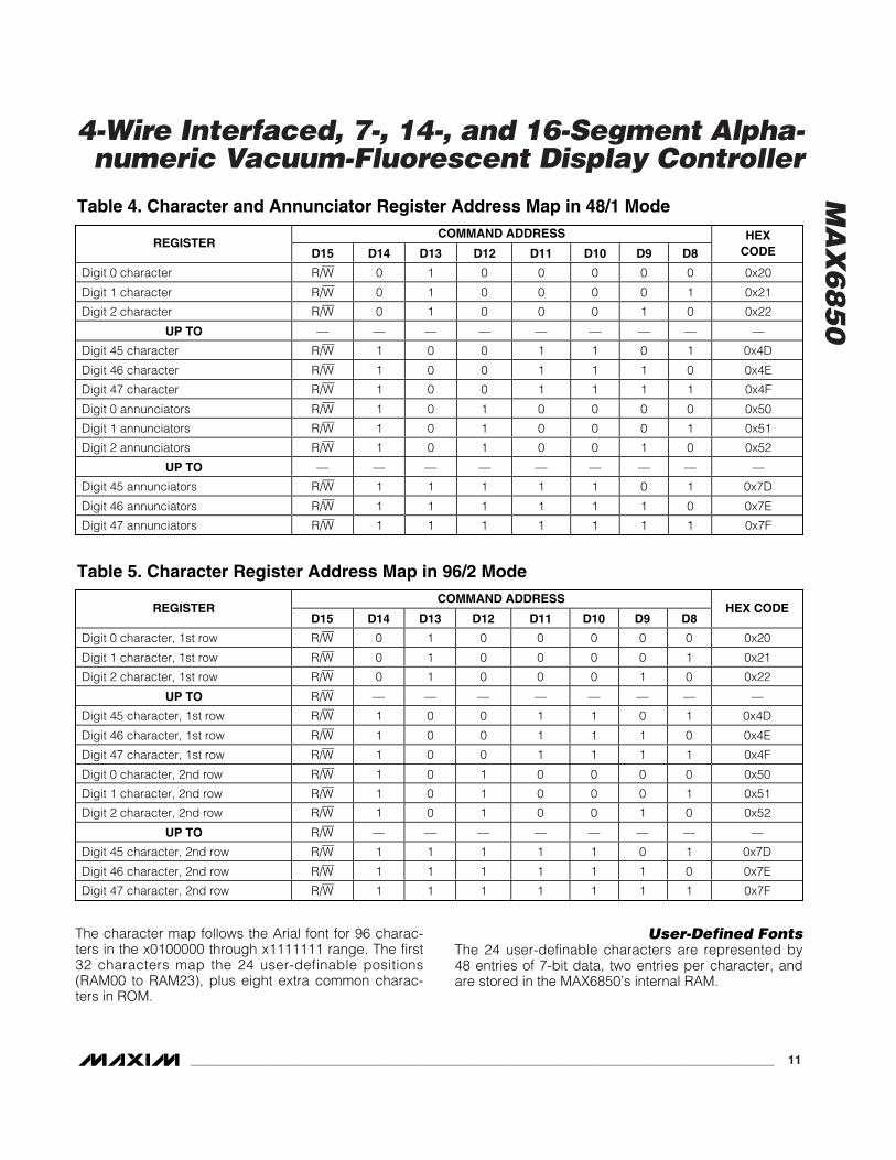
Character RegistersThe MAX6850 uses 48 character registers (48/1 mode)(Table 4) or 96 character registers (96/2 mode) (Table5) to store the 7-, 14-, and 16-segment characters(Table 6). Each digit is represented by 1 byte of memo-ry. The data in the character registers does not controlthe character segments directly. Instead, the registerdata is used to address a character generator, whichstores the data of the 128-character font (Table 7). Thelower 7 bits of the character data (D6 to D0) select acharacter from the font table. The most significant bit(MSB) of the register data (D7) controls the DP seg-ment of the digit; it is set to light the DP, cleared toleave it unlit.
The character registers address maps are shown inTable 4 (48/1 mode) and Table 5 (96/2 mode).
In 48/1 mode, the character registers use a singleaddress range 0x20 to 0x20 + g, where g is the valuein the grids register (Table 26). The 48/1 mode upperaddress limit, when g is 0x2F, is therefore 0x4F. Theaddress range 0x50 to 0x7F is used for annunciatordata in 48/1 mode.
In 96/2 mode, the character registers use two addressranges. The first row ’s address range is 0x20 to 0x20 + g. The second row’s address range is 0x50 to0x50 + g. Therefore, in 96/2 mode, the character reg-isters are only one contiguous memory range when a48-grid display is used.
DISPLAYMODE
MAXIMUM NO. OF DIGITSMAXIMUM NO. OFANNUNCIATORS
MAXIMUM NO.OF GRIDS
DIGITS COVEREDBY EACH GRID
48/1 mode48 digits, each with a DP segment and a cursorsegment
4 per digit 1 digit per grid
96/2 mode96 digits, each with a DP segment and a cursorsegment
None48 grids
2 digits per grid
Table 1. Display Modes
COMMAND ADDRESSREGISTER
D15 D14 D13 D12 D11 D10 D9 D8HEX
CODE
No-Op R/W 0 0 0 0 0 0 0 0x00
VFBLANK polarity R/W 0 0 0 0 0 0 1 0x01
Intensity R/W 0 0 0 0 0 1 0 0x02
Grids R/W 0 0 0 0 0 1 1 0x03
Configuration R/W 0 0 0 0 1 0 0 0x04
User-defined fonts R/W 0 0 0 0 1 0 1 0x05
Output map R/W 0 0 0 0 1 1 0 0x06
Display test and device ID R/W 0 0 0 0 1 1 1 0x07
PUMP register R/W 0 0 0 1 0 0 0 0x08
Filament duty cycle R/W 0 0 0 1 0 0 1 0x09
PHASE1 R/W 0 0 0 1 0 1 0 0x0A
PHASE2 R/W 0 0 0 1 0 1 1 0x0B
PORT0 R/W 0 0 0 1 1 0 0 0x0C
PORT1 R/W 0 0 0 1 1 0 1 0x0D
Shift limit R/W 0 0 0 1 1 1 0 0x0E
Cursor R/W 0 0 0 1 1 1 1 0x0F
Factory reserved. Do not write to register. X 0 0 1 0 0 0 0 0x10
Table 2. Register Address Map
MA
X6
85
0
4-Wire Interfaced, 7-, 14-, and 16-Segment Alpha-numeric Vacuum-Fluorescent Display Controller
10 ______________________________________________________________________________________
Character Generator Font MappingThe font comprises 104 characters in ROM, and 24user-definable characters. The selection from the totalof 128 characters is represented by the lower 7 bits ofthe 8-bit digit registers. The MSB, shown as X in theROM maps (Tables 7 and 8), controls the DP segmentof the digit; it is set to light the DP.
There are two font maps stored in the MAX6850. Onefont map covers 14-segment displays (Table 8), andthe other suits 16-segment displays (Table 7). The F bitin the configuration register (Table 20) selects betweenthe two font maps. The F bit may be set either high orlow for 7-segment displays; 7-segment displays use asubset of the 14- or 16-segment display described intwo font maps (Figure 7).
REGISTER DATAREGISTER POWER-UP CONDITION
COMMANDADDRESS D7 D6 D5 D4 D3 D2 D1 D0
VFBLANK polarityVFBLANK is high to disable thedisplay
0x01 X X X X X X 0 0
Intensity 1/16 (min on) 0x02 X X X X 0 0 0 0
Grids Display has 1 grid 0x03 X X 0 0 0 0 0 0
ConfigurationShutdown enabled,configuration unlocked
0x04 1 0 0 0 0 0 0 0
User-defined fontaddress pointer
Address 0x80; pointing to thefirst user-defined font location
0x05 1 0 0 0 0 0 0 0
User-defined fonts Predefined for hex fonts — See Table 11 for power-up patterns.
Output map pointerAddress 0x80; pointing to thefirst entry address
0x06 1 0 0 0 0 0 0 0
Output map data Predefined for 40-digit display — See Table 32 for power-up patterns.
Display test Normal operation 0x07 X X X X X X X 0
PUMP General-purpose output, logic 0x08 0 0 0 0 0 0 0 0
Filament duty cycle Minimum duty cycle 0x09 0 0 0 0 0 0 0 1
PHASE1 General-purpose output, logic 0x0A 0 0 0 0 0 0 0 0
PHASE2 General-purpose output, logic 0x0B 0 0 0 0 0 0 0 0
PORT0 General-purpose output, logic 0x0C 0 0 0 0 0 0 0 0
PORT1 General-purpose output, logic 0x0D 0 0 0 0 0 0 0 1
Shift limit 1 output bit 0x0E X 0 0 0 0 0 0 1
Cursor Off 0x0F 0 1 1 0 0 0 0 0
Character andannunciator data
Clear 0x20 0 0 0 0 0 0 0 0
UP TO — UP TO — — — — — — — —
Character andannunciator data
Clear 0x7F 0 0 0 0 0 0 0 0
Table 3. Initial Power-Up Register Status
MAPS TO
7 SEGMENT 14/16 SEGMENT
dp dp
a
g
d
e c
f b
a/a1
g1
d/d2
e c
f b
Figure 7. 14- and 16-Segment Fonts Map a Subset of Their 14or 16 Segments to a 7-Segment Digit
MA
X6
85
0
4-Wire Interfaced, 7-, 14-, and 16-Segment Alpha-numeric Vacuum-Fluorescent Display Controller
______________________________________________________________________________________ 11
The character map follows the Arial font for 96 charac-ters in the x0100000 through x1111111 range. The first32 characters map the 24 user-definable positions(RAM00 to RAM23), plus eight extra common charac-ters in ROM.
User-Defined FontsThe 24 user-definable characters are represented by48 entries of 7-bit data, two entries per character, andare stored in the MAX6850’s internal RAM.
COMMAND ADDRESSREGISTER
D15 D14 D13 D12 D11 D10 D9 D8HEX
CODE
Digit 0 character R/W 0 1 0 0 0 0 0 0x20
Digit 1 character R/W 0 1 0 0 0 0 1 0x21
Digit 2 character R/W 0 1 0 0 0 1 0 0x22
UP TO — — — — — — — — —
Digit 45 character R/W 1 0 0 1 1 0 1 0x4D
Digit 46 character R/W 1 0 0 1 1 1 0 0x4E
Digit 47 character R/W 1 0 0 1 1 1 1 0x4F
Digit 0 annunciators R/W 1 0 1 0 0 0 0 0x50
Digit 1 annunciators R/W 1 0 1 0 0 0 1 0x51
Digit 2 annunciators R/W 1 0 1 0 0 1 0 0x52
UP TO — — — — — — — — —
Digit 45 annunciators R/W 1 1 1 1 1 0 1 0x7D
Digit 46 annunciators R/W 1 1 1 1 1 1 0 0x7E
Digit 47 annunciators R/W 1 1 1 1 1 1 1 0x7F
Table 4. Character and Annunciator Register Address Map in 48/1 Mode
Table 5. Character Register Address Map in 96/2 ModeCOMMAND ADDRESS
REGISTERD15 D14 D13 D12 D11 D10 D9 D8
HEX CODE
Digit 0 character, 1st row R/W 0 1 0 0 0 0 0 0x20
Digit 1 character, 1st row R/W 0 1 0 0 0 0 1 0x21
Digit 2 character, 1st row R/W 0 1 0 0 0 1 0 0x22
UP TO R/W — — — — — — — —
Digit 45 character, 1st row R/W 1 0 0 1 1 0 1 0x4D
Digit 46 character, 1st row R/W 1 0 0 1 1 1 0 0x4E
Digit 47 character, 1st row R/W 1 0 0 1 1 1 1 0x4F
Digit 0 character, 2nd row R/W 1 0 1 0 0 0 0 0x50
Digit 1 character, 2nd row R/W 1 0 1 0 0 0 1 0x51
Digit 2 character, 2nd row R/W 1 0 1 0 0 1 0 0x52
UP TO R/W — — — — — — — —
Digit 45 character, 2nd row R/W 1 1 1 1 1 0 1 0x7D
Digit 46 character, 2nd row R/W 1 1 1 1 1 1 0 0x7E
Digit 47 character, 2nd row R/W 1 1 1 1 1 1 1 0x7F

MA
X6
85
0
4-Wire Interfaced, 7-, 14-, and 16-Segment Alpha-numeric Vacuum-Fluorescent Display Controller
12 ______________________________________________________________________________________
The user-definable characters are preloaded on power-up with 24 fonts. These fonts are intended to be useful for7-segment displays, and include the hexadecimal set forthe first 16 characters, plus eight other useful segmentcombinations. Table 12 shows how the 14-segment and16-segment fonts map to 7-segment displays.
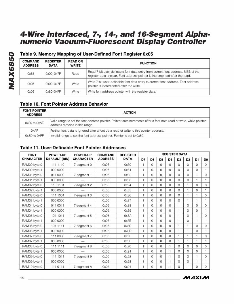
The 48 user-definable font data entries are written andread through a single register, address 0x05. Anautoincrementing font address pointer in the MAX6850indirectly accesses the font data. The font addresspointer can be written, setting one of 48 addressesbetween 0x00 and 0x2F, but cannot be read back. Thefont data is written to and read from the MAX6850 indi-rectly, using this font address pointer. Unused fontlocations can be used as general-purpose scratchRAM, bearing in mind that the font registers are only 7bits wide, not 8.
Table 9 shows how to use the single user-defined fontregister 0x05 to set the font address pointer, write fontdata, and read font data. A read action always returnsfont data from the font address pointer position. A writeaction sets the 7-bit font address pointer if the MSB isset, or writes 7-bit font data to the font address pointerposition if the MSB is clear.
The font address pointer autoincrements after a validaccess to the user-definable font data. Autoincrementingallows the 48-font data entries to be written and readback very quickly because the font pointer addressneeds be set only once. After the last data location 0x2Fhas been written, further font data entries are ignored untilthe font address pointer is reset. If the font address point-er is set to an out-of-range address by writing data in the0xB0 to 0xFF range, then address 0x80 is set instead(Table 10).
Table 11 shows the user-definable font pointer ad-dresses.
Table 12 shows bit/segment mapping for user-definedfonts when applied to 7-, 14-, or 16-segment digits.
Table 13 illustrates how to set the font address pointerto a value within the acceptable range. D7 is set (1) todenote that the user is writing the font address pointer.If the user attempts to set the font address to one of theout-of-range addresses by writing data in range 0xB0to 0xFF, then address 0x00 is set instead.
The font address pointer autoincrements from address(the last user font location) to point to address 0x00 (thefirst user font location). Thus, the font address pointerautoincrements indefinitely through font RAM.
Cursor RegisterThe cursor register controls the behavior of the cursorsegments (Table 14). The MAX6850 controls 48 cursorsin 48/1 mode, and 96 cursors in 96/2 mode. The cursorregister selects one digit’s cursor to be lit either contin-uously or blinking. All the other digits’ cursors are off.
The 7 least significant bits (LSBs) of the cursor registeridentify the cursor position. The MSB is clear for thecursor to be on continuously, and set for the cursor tobe lit only during the first half of each blink period.
The valid cursor position address range is contiguous:0 to 47 (0x00 to 0x2F) for the first row, and 48 to 95(0x30 to 0x5F) for the 2nd row. If the cursor register isprogrammed with an out-of-range value of 95 to 127(0x60 to 0x7F), then all cursors are off.
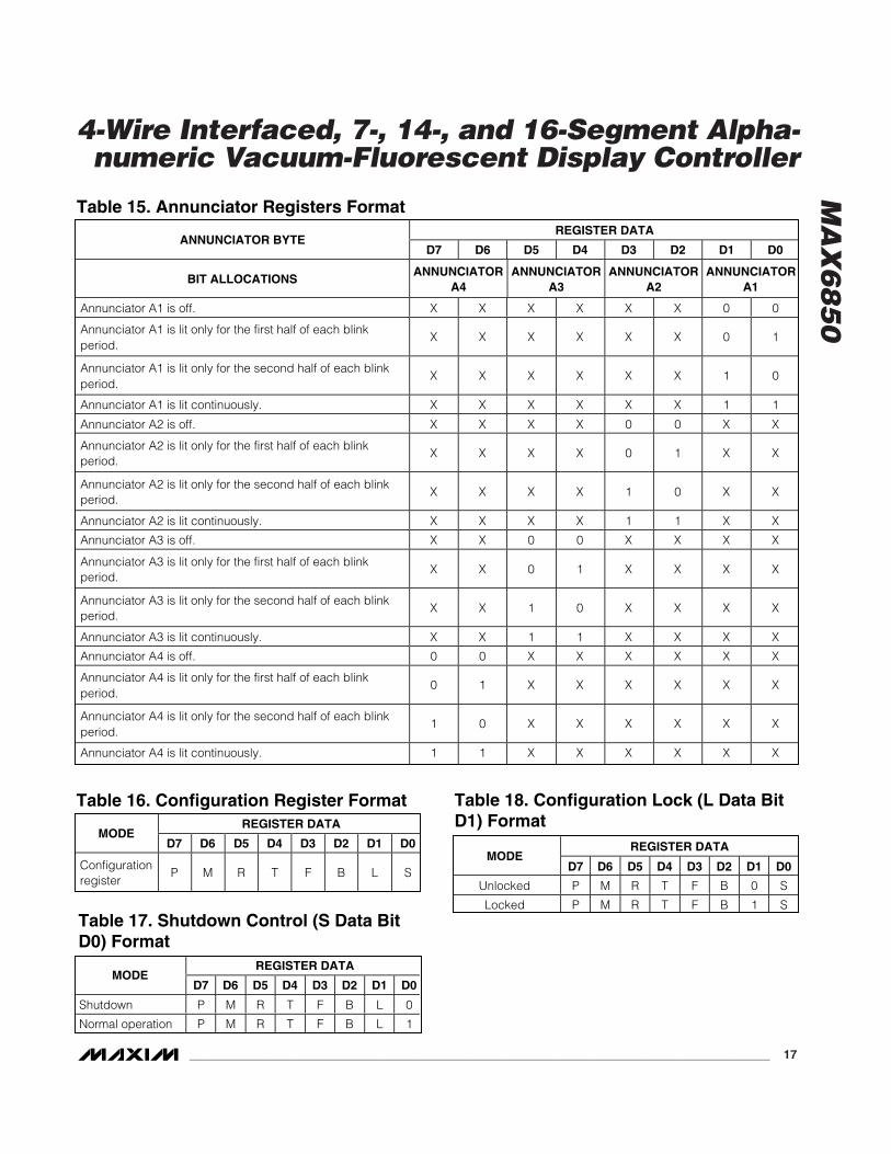
Annunciator RegistersThe annunciator registers are organized in bytes, witheach segment of each grid being represented by 2bits. Thus, the four annunciators segments allowed foreach grid are represented by exactly 1 byte (Table 15).Annunciators are only available in 48/1 mode. Theannunciator address map is shown in Table 4.
Configuration RegisterThe configuration register is used to enter and exit shut-down, lock the key VFD configuration settings, selectthe blink rate, globally clear the digit and annunciatordata, reset the blink timing, and select between 48/1and 96/2 display modes (Table 16).
REGISTER DATAMODE COMMAND ADDRESS
D7 D6 D5 D4 D3 D2 D1 D0
Writing character data to use font mapdata with DP segment unlit
0x20 to 0x4F (48/1 mode)0x20 to 0x7F (96/2 mode)
0
Writing character data to use font mapdata with DP segment lit
0x20 to 0x4F (48/1 mode)0x20 to 0x7F (96/2 mode)
1
Bits D6 to D0 select font characters 0 to 127
Table 6. Character Registers Format

MA
X6
85
0
4-Wire Interfaced, 7-, 14-, and 16-Segment Alpha-numeric Vacuum-Fluorescent Display Controller
______________________________________________________________________________________ 13
x000 x010 x011 x100 x101 x110 x111x001
0000
0001
0010
0011
0100
0101
0110
0111
1000
1001
1010
1011
1100
1101
1110
1111
MSBLSB
RAM00
RAM01
RAM02
RAM03
RAM04
RAM05
RAM06
RAM07
RAM08
RAM09
RAM0A
RAM0B
RAM0C
RAM0D
RAM0E
RAM0F
RAM10
RAM11
RAM12
RAM13
RAM14
RAM15
RAM16
RAM17
Table 7. 16-Segment Display Font Map
x000 x010 x011 x100 x101 x110 x111x001
0000
0001
0010
0011
0100
0101
0110
0111
1000
1001
1010
1011
1100
1101
1110
1111
MSBLSB
RAM00
RAM01
RAM02
RAM03
RAM04
RAM05
RAM06
RAM07
RAM08
RAM09
RAM0A
RAM0B
RAM0C
RAM0D
RAM0E
RAM0F
RAM10
RAM11
RAM12
RAM13
RAM14
RAM15
RAM16
RAM17
Table 8. 14-Segment Display Font Map
MA
X6
85
0
4-Wire Interfaced, 7-, 14-, and 16-Segment Alpha-numeric Vacuum-Fluorescent Display Controller
14 ______________________________________________________________________________________
COMMANDADDRESS
REGISTERDATA
READ ORWRITE
FUNCTION
0x85 0x00–0x7F ReadRead 7-bit user-definable font data entry from current font address. MSB of theregister data is clear. Font address pointer is incremented after the read.
0x05 0x00–0x7F WriteWrite 7-bit user-definable font data entry to current font address. Font addresspointer is incremented after the write.
0x05 0x80–0xFF Write Write font address pointer with the register data.
Table 9. Memory Mapping of User-Defined Font Register 0x05
FONT POINTERADDRESS
ACTION
0x80 to 0xAEValid range to set the font address pointer. Pointer autoincrements after a font data read or write, while pointeraddress remains in this range.
0xAF Further font data is ignored after a font data read or write to this pointer address.
0xB0 to 0xFF Invalid range to set the font address pointer. Pointer is set to 0x80.
Table 10. Font Pointer Address Behavior
REGISTER DATAFONTCHARACTER
POWER-UPDEFAULT (BIN)
POWER-UPCHARACTER
COMMANDADDRESS
REGISTERDATA D7 D6 D5 D4 D3 D2 D1 D0
RAM00 byte 0 111 1110 7-segment 0 0x05 0x80 1 0 0 0 0 0 0 0
RAM00 byte 1 000 0000 — 0x05 0x81 1 0 0 0 0 0 0 1
RAM01 byte 0 011 0000 7-segment 1 0x05 0x82 1 0 0 0 0 0 1 0
RAM01 byte 1 000 0000 — 0x05 0x83 1 0 0 0 0 0 1 1
RAM02 byte 0 110 1101 7-segment 2 0x05 0x84 1 0 0 0 0 1 0 0
RAM02 byte 1 000 0000 — 0x05 0x85 1 0 0 0 0 1 0 1
RAM03 byte 0 111 1001 7-segment 3 0x05 0x86 1 0 0 0 0 1 1 0
RAM03 byte 1 000 0000 — 0x05 0x87 1 0 0 0 0 1 1 1
RAM04 byte 0 011 0011 7-segment 4 0x05 0x88 1 0 0 0 1 0 0 0
RAM04 byte 1 000 0000 — 0x05 0x89 1 0 0 0 1 0 0 1
RAM05 byte 0 101 1011 7-segment 5 0x05 0x8A 1 0 0 0 1 0 1 0
RAM05 byte 1 000 0000 — 0x05 0x8B 1 0 0 0 1 0 1 1
RAM06 byte 0 101 1111 7-segment 6 0x05 0x8C 1 0 0 0 1 1 0 0
RAM06 byte 1 000 0000 — 0x05 0x8D 1 0 0 0 1 1 0 1
RAM07 byte 0 111 0000 7-segment 7 0x05 0x8E 1 0 0 0 1 1 1 0
RAM07 byte 1 000 0000 — 0x05 0x8F 1 0 0 0 1 1 1 1
RAM08 byte 0 111 1111 7-segment 8 0x05 0x90 1 0 0 1 0 0 0 0
RAM08 byte 1 000 0000 — 0x05 0x91 1 0 0 1 0 0 0 1
RAM09 byte 0 111 1011 7-segment 9 0x05 0x92 1 0 0 1 0 0 1 0
RAM09 byte 1 000 0000 — 0x05 0x93 1 0 0 1 0 0 1 1
RAM10 byte 0 111 0111 7-segment A 0x05 0x94 1 0 0 1 0 1 0 0
Table 11. User-Definable Font Pointer Addresses
MA
X6
85
0
4-Wire Interfaced, 7-, 14-, and 16-Segment Alpha-numeric Vacuum-Fluorescent Display Controller
______________________________________________________________________________________ 15
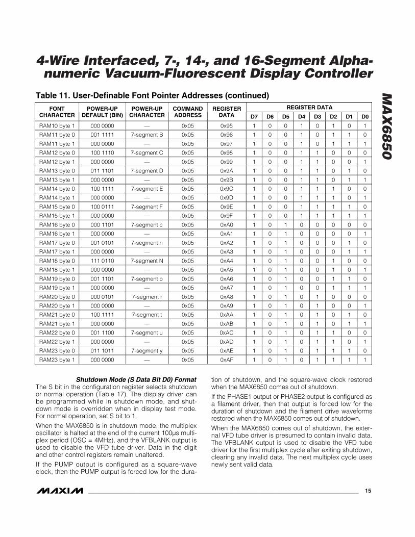
Shutdown Mode (S Data Bit D0) FormatThe S bit in the configuration register selects shutdownor normal operation (Table 17). The display driver canbe programmed while in shutdown mode, and shut-down mode is overridden when in display test mode.For normal operation, set S bit to 1.
When the MAX6850 is in shutdown mode, the multiplexoscillator is halted at the end of the current 100µs multi-plex period (OSC = 4MHz), and the VFBLANK output isused to disable the VFD tube driver. Data in the digitand other control registers remain unaltered.
If the PUMP output is configured as a square-waveclock, then the PUMP output is forced low for the dura-
tion of shutdown, and the square-wave clock restoredwhen the MAX6850 comes out of shutdown.
If the PHASE1 output or PHASE2 output is configured asa filament driver, then that output is forced low for theduration of shutdown and the filament drive waveformsrestored when the MAX6850 comes out of shutdown.
When the MAX6850 comes out of shutdown, the exter-nal VFD tube driver is presumed to contain invalid data.The VFBLANK output is used to disable the VFD tubedriver for the first multiplex cycle after exiting shutdown,clearing any invalid data. The next multiplex cycle usesnewly sent valid data.
REGISTER DATAFONTCHARACTER
POWER-UPDEFAULT (BIN)
POWER-UPCHARACTER
COMMANDADDRESS
REGISTERDATA D7 D6 D5 D4 D3 D2 D1 D0
RAM10 byte 1 000 0000 — 0x05 0x95 1 0 0 1 0 1 0 1
RAM11 byte 0 001 1111 7-segment B 0x05 0x96 1 0 0 1 0 1 1 0
RAM11 byte 1 000 0000 — 0x05 0x97 1 0 0 1 0 1 1 1
RAM12 byte 0 100 1110 7-segment C 0x05 0x98 1 0 0 1 1 0 0 0
RAM12 byte 1 000 0000 — 0x05 0x99 1 0 0 1 1 0 0 1
RAM13 byte 0 011 1101 7-segment D 0x05 0x9A 1 0 0 1 1 0 1 0
RAM13 byte 1 000 0000 — 0x05 0x9B 1 0 0 1 1 0 1 1
RAM14 byte 0 100 1111 7-segment E 0x05 0x9C 1 0 0 1 1 1 0 0
RAM14 byte 1 000 0000 — 0x05 0x9D 1 0 0 1 1 1 0 1
RAM15 byte 0 100 0111 7-segment F 0x05 0x9E 1 0 0 1 1 1 1 0
RAM15 byte 1 000 0000 — 0x05 0x9F 1 0 0 1 1 1 1 1
RAM16 byte 0 000 1101 7-segment c 0x05 0xA0 1 0 1 0 0 0 0 0
RAM16 byte 1 000 0000 — 0x05 0xA1 1 0 1 0 0 0 0 1
RAM17 byte 0 001 0101 7-segment n 0x05 0xA2 1 0 1 0 0 0 1 0
RAM17 byte 1 000 0000 — 0x05 0xA3 1 0 1 0 0 0 1 1
RAM18 byte 0 111 0110 7-segment N 0x05 0xA4 1 0 1 0 0 1 0 0
RAM18 byte 1 000 0000 — 0x05 0xA5 1 0 1 0 0 1 0 1
RAM19 byte 0 001 1101 7-segment o 0x05 0xA6 1 0 1 0 0 1 1 0
RAM19 byte 1 000 0000 — 0x05 0xA7 1 0 1 0 0 1 1 1
RAM20 byte 0 000 0101 7-segment r 0x05 0xA8 1 0 1 0 1 0 0 0
RAM20 byte 1 000 0000 — 0x05 0xA9 1 0 1 0 1 0 0 1
RAM21 byte 0 100 1111 7-segment t 0x05 0xAA 1 0 1 0 1 0 1 0
RAM21 byte 1 000 0000 — 0x05 0xAB 1 0 1 0 1 0 1 1
RAM22 byte 0 001 1100 7-segment u 0x05 0xAC 1 0 1 0 1 1 0 0
RAM22 byte 1 000 0000 — 0x05 0xAD 1 0 1 0 1 1 0 1
RAM23 byte 0 011 1011 7-segment y 0x05 0xAE 1 0 1 0 1 1 1 0
RAM23 byte 1 000 0000 — 0x05 0xAF 1 0 1 0 1 1 1 1
Table 11. User-Definable Font Pointer Addresses (continued)

MA
X6
85
0
4-Wire Interfaced, 7-, 14-, and 16-Segment Alpha-numeric Vacuum-Fluorescent Display Controller
16 ______________________________________________________________________________________
BIT/SEGMENT MAPPING FOR USER-DEFINABLE FONTS WHEN APPLIED TO 7-SEGMENT DIGITS
FONT BYTE BIT 6 BIT 5 BIT 4 BIT 3 BIT 2 BIT 1 BIT 0
RAMxx byte 0 7-seg a 7-seg b 7-seg c 7-seg d 7-seg e 7-seg f 7-seg g
RAMxx byte 1 No action No action No action No action No action No action No action
BIT/SEGMENT MAPPING FOR USER-DEFINABLE FONTS WHEN APPLIED TO 14-SEGMENT DIGITS
FONT BYTE BIT 6 BIT 5 BIT 4 BIT 3 BIT 2 BIT 1 BIT 0
RAMxx byte 0 7-seg a 7-seg b 7-seg c 7-seg d 7-seg e 7-seg f 7-seg g1
RAMxx byte 1 14-seg g2 14-seg h 14-seg i 14-seg j 14-seg k 14-seg l 14-seg m
BIT/SEGMENT MAPPING FOR USER-DEFINABLE FONTS WHEN APPLIED TO 16-SEGMENT DIGITS
FONT BYTE BIT 6 BIT 5 BIT 4 BIT 3 BIT 2 BIT 1 BIT 0
RAMxx byte 0 7-seg a1 7-seg b 7-seg c 7-seg d2 7-seg e 7-seg f 7-seg g1
RAMxx byte 1 14-seg g2 14-seg h 14-seg i 14-seg j 14-seg k 14-seg l 14-seg m
Table 12. User-Definable Character Mapping
REGISTER DATAMODE
COMMANDADDRESS D7 D6 D5 D4 D3 D2 D1 D0
Set font address to minimum (zero) with data 128 or0x80. (Note that this address is set as power-up default.)
0x05 1 0 0 0 0 0 0 0
Set font address to maximum (47 or 0x2F) with data 175or 0xAF.
0x05 1 0 1 0 1 1 1 1
Set font address out of range (48 or 0x30) with data 176or 0xB0 results in font address pointer being set to zero.
0x05 1 1 1 1 1 0 0 0
UP TO UP TO
Set font address out of range (127 or 0x7F) with data 255or 0xFF results in font address pointer being set to zero.
0x05 1 1 1 1 1 1 1 1
Read font address. 0x85 0 Font address; has value 0x00 to 0xA7
Table 13. Setting a Font Character to RAM
REGISTER DATAMODE
COMMANDADDRESS D7 D6 D5 D4 D3 D2 D1 D0
Cursor register. 0x0F BLINK CURSOR POSITION
1st row digit 0's cursor is lit continuously. 0x0F 0 0 0 0 0 0 0 0
1st row digit 0's cursor is lit only for the first half of eachblink period.
0x0F 1 0 0 0 0 0 0 0
UP TO UP TO
2nd row digit 47's cursor is lit continuously. 0x0F 0 1 0 1 1 1 1 1
2nd row digit 47's cursor is lit only for the first half of eachblink period.
0x0F 1 1 0 1 1 1 1 1
No cursor is lit. 0x0F X 1 1 X X X X X
Table 14. Cursor Register Format
MA
X6
85
0
4-Wire Interfaced, 7-, 14-, and 16-Segment Alpha-numeric Vacuum-Fluorescent Display Controller
______________________________________________________________________________________ 17
REGISTER DATAANNUNCIATOR BYTE
D7 D6 D5 D4 D3 D2 D1 D0
BIT ALLOCATIONSANNUNCIATOR
A4ANNUNCIATOR
A3ANNUNCIATOR
A2ANNUNCIATOR
A1
Annunciator A1 is off. X X X X X X 0 0
Annunciator A1 is lit only for the first half of each blinkperiod.
X X X X X X 0 1
Annunciator A1 is lit only for the second half of each blinkperiod.
X X X X X X 1 0
Annunciator A1 is lit continuously. X X X X X X 1 1
Annunciator A2 is off. X X X X 0 0 X X
Annunciator A2 is lit only for the first half of each blinkperiod.
X X X X 0 1 X X
Annunciator A2 is lit only for the second half of each blinkperiod.
X X X X 1 0 X X
Annunciator A2 is lit continuously. X X X X 1 1 X X
Annunciator A3 is off. X X 0 0 X X X X
Annunciator A3 is lit only for the first half of each blinkperiod.
X X 0 1 X X X X
Annunciator A3 is lit only for the second half of each blinkperiod.
X X 1 0 X X X X
Annunciator A3 is lit continuously. X X 1 1 X X X X
Annunciator A4 is off. 0 0 X X X X X X
Annunciator A4 is lit only for the first half of each blinkperiod.
0 1 X X X X X X
Annunciator A4 is lit only for the second half of each blinkperiod.
1 0 X X X X X X
Annunciator A4 is lit continuously. 1 1 X X X X X X
Table 15. Annunciator Registers Format
REGISTER DATAMODE
D7 D6 D5 D4 D3 D2 D1 D0
Configurationregister
P M R T F B L S
Table 16. Configuration Register Format
REGISTER DATAMODE
D7 D6 D5 D4 D3 D2 D1 D0
Unlocked P M R T F B 0 S
Locked P M R T F B 1 S
Table 18. Configuration Lock (L Data BitD1) Format
REGISTER DATAMODE
D7 D6 D5 D4 D3 D2 D1 D0
Shutdown P M R T F B L 0
Normal operation P M R T F B L 1
Table 17. Shutdown Control (S Data BitD0) Format

MA
X6
85
0
4-Wire Interfaced, 7-, 14-, and 16-Segment Alpha-numeric Vacuum-Fluorescent Display Controller
18 ______________________________________________________________________________________
Configuration Lock (L Data Bit D1) FormatThe configuration lock register is a safety feature toreduce the risk of the VFD configuration settings beinginadvertently changed due to spurious writes if soft-ware fails. When set, the shift-limit register (0x0E), gridsregister (0x03), and output map data (0x06) can beread but cannot be written. The output map data point-er itself may be written in order to allow the output mapdata to be read back (Table 18).
Blink Rate Selection (B Data Bit D2) FormatThe B bit in the configuration register selects the blinkrate of the cursor and annunciator segments. This is thespeed that the segments blink on and off when blinkingis selected for these segments. The frequency of themultiplex clock OSC and the setting of the B bit (Table19) determine the blink rate.
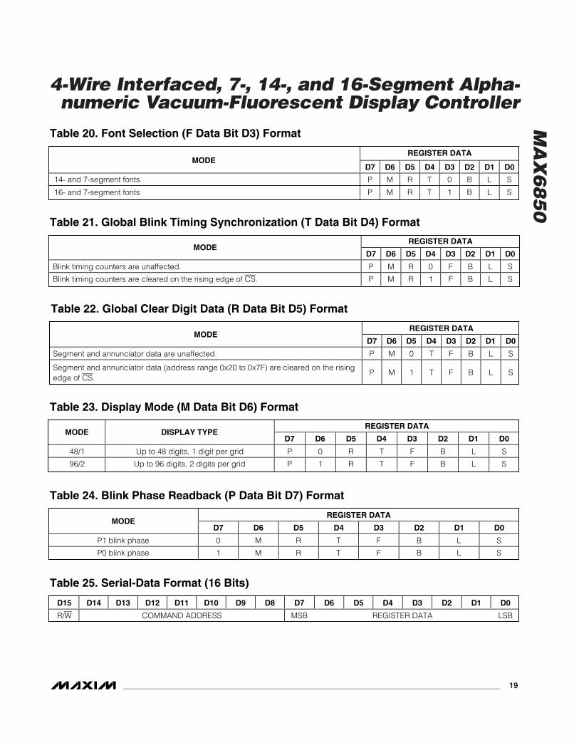
Font Selection (F Data Bit D3) FormatThe F bit (Table 20) selects the internal font mapbetween 14-segment and 16-segment displays. If a 7-segment display is used, the F bit can be either set orcleared.
Global Blink Timing Synchronization (T Data Bit D4) Format
Setting the T bit in multiple MAX6850s at the same time(or in quick succession) synchronizes the blink timingacross all the devices (Table 21). The display multiplex-ing sequence is also reset, which can give rise to aone-time display flicker when the register is written.
Global Clear Digit Data (R Data Bit D5) FormatWhen the R bit (Table 22) is set, the segment andannunciator data are cleared.
Display Mode (M Data Bit D6) FormatThe M bit (Table 23) selects the display modes (Table 1).The display modes trade the maximum allowable number of digits (mode 96/2) against the availability ofannunciator segments (mode 48/1).
Blink Phase Readback (P Data Bit D7) FormatWhen the configuration register is read, the P bitreflects the blink phase at that time (Table 24).
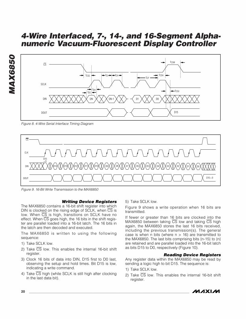
Microcontroller 4-Wire Serial InterfaceThe MAX6850 communicates through an SPI-compati-ble 4-wire serial interface (Figure 8). The interface hasthree inputs, clock (SCLK), chip select (CS), data in(DIN), and output data out (DOUT). CS must be low toclock data into or out of the device, and DIN must bestable when sampled on the rising edge of SCLK.DOUT is not a specific pin, but instead, any of thePUMP, PORT0, or PORT1 outputs can be configured tobe DOUT. DOUT is stable on the rising edge of SCLK.While the SPI protocol expects DOUT to be highimpedance when the MAX6850 is not being accessed,DOUT on the MAX6850 is never high impedance. SCLKand DIN can be used to transmit data to other peripher-als. The MAX6850 ignores all activity on SCLK and DINexcept when CS is low.
Control and Operation Using the 4-WireInterface
Controlling the MAX6850 requires sending a 16-bitword. The first byte, D15 through D8, is the commandaddress, and the second byte, D7 through D0, is thedata to be written to the command address (Table 25).
Connecting Multiple MAX6850s to the 4-Wire Bus
Daisy-chain multiple MAX6850s by connecting theDOUT of one device to the DIN of the next, and drivingSCLK and CS lines in parallel. Data at DIN propagatesthrough the internal shift registers and appears atDOUT 15.5 clock cycles later, clocked out on the risingedge of SCLK. When sending commands to daisy-chained MAX6850s, all devices are accessed at thesame time. An access requires (16 x n) clock cycles,where n is the number of MAX6850s connected togeth-er. To update just one device in a daisy-chain, send theno-op command (0x00) to the others. Care must betaken on power-up when daisy-chaining the serial inter-face in this manner. Configure each MAX6850’s PORT0or PORT1 outputs, in turn, to act as DOUT before datapropagates through it. For this reason, PORT0 is thepreferred output to configure as DOUT because its out-put on power-up is low. This means that a daisy-chained DIN input taking data from an uninitializedPORT0 output clocks in 16 logic zeros, which is thesafe no-op instruction.
REGISTER DATAMODE
D7 D6 D5 D4 D3 D2 D1 D0
Slow blinking (cursor and annunciators blink on for 1s, off for 1s, for OSC = 4MHz) P M R T F 0 L S
Fast blinking (cursor and annunciators blink on for 0.5s, off for 0.5s, for OSC = 4MHz) P M R T F 1 L S
Table 19. Blink Rate Selection (B Data Bit D2) Format
MA
X6
85
0
4-Wire Interfaced, 7-, 14-, and 16-Segment Alpha-numeric Vacuum-Fluorescent Display Controller
______________________________________________________________________________________ 19
REGISTER DATAMODE
D7 D6 D5 D4 D3 D2 D1 D0
14- and 7-segment fonts P M R T 0 B L S
16- and 7-segment fonts P M R T 1 B L S
Table 20. Font Selection (F Data Bit D3) Format
REGISTER DATAMODE
D7 D6 D5 D4 D3 D2 D1 D0
Blink timing counters are unaffected. P M R 0 F B L S
Blink timing counters are cleared on the rising edge of CS. P M R 1 F B L S
Table 21. Global Blink Timing Synchronization (T Data Bit D4) Format
REGISTER DATAMODE
D7 D6 D5 D4 D3 D2 D1 D0
Segment and annunciator data are unaffected. P M 0 T F B L S
Segment and annunciator data (address range 0x20 to 0x7F) are cleared on the risingedge of CS.
P M 1 T F B L S
Table 22. Global Clear Digit Data (R Data Bit D5) Format
REGISTER DATAMODE DISPLAY TYPE
D7 D6 D5 D4 D3 D2 D1 D0
48/1 Up to 48 digits, 1 digit per grid P 0 R T F B L S
96/2 Up to 96 digits, 2 digits per grid P 1 R T F B L S
Table 23. Display Mode (M Data Bit D6) Format
REGISTER DATAMODE
D7 D6 D5 D4 D3 D2 D1 D0
P1 blink phase 0 M R T F B L S
P0 blink phase 1 M R T F B L S
Table 24. Blink Phase Readback (P Data Bit D7) Format
D15 D14 D13 D12 D11 D10 D9 D8 D7 D6 D5 D4 D3 D2 D1 D0
R/W COMMAND ADDRESS MSB REGISTER DATA LSB
Table 25. Serial-Data Format (16 Bits)
MA
X6
85
0
4-Wire Interfaced, 7-, 14-, and 16-Segment Alpha-numeric Vacuum-Fluorescent Display Controller
20 ______________________________________________________________________________________
Writing Device RegistersThe MAX6850 contains a 16-bit shift register into whichDIN is clocked on the rising edge of SCLK, when CS islow. When CS is high, transitions on SCLK have noeffect. When CS goes high, the 16 bits in the shift regis-ter are parallel loaded into a 16-bit latch. The 16 bits inthe latch are then decoded and executed.
The MAX6850 is written to using the followingsequence:
1) Take SCLK low.
2) Take CS low. This enables the internal 16-bit shiftregister.
3) Clock 16 bits of data into DIN, D15 first to D0 last,observing the setup and hold times. Bit D15 is low,indicating a write command.
4) Take CS high (while SCLK is still high after clockingin the last data bit).
5) Take SCLK low.
Figure 9 shows a write operation when 16 bits aretransmitted.
If fewer or greater than 16 bits are clocked into theMAX6850 between taking CS low and taking CS highagain, the MAX6850 stores the last 16 bits received,including the previous transmission(s). The generalcase is when n bits (where n > 16) are transmitted tothe MAX6850. The last bits comprising bits n-15 to nare retained and are parallel loaded into the 16-bit latchas bits D15 to D0, respectively (Figure 10).
Reading Device RegistersAny register data within the MAX6850 may be read bysending a logic high to bit D15. The sequence is:
1) Take SCLK low.
2) Take CS low. This enables the internal 16-bit shiftregister.
CS
CLK
DIN
D15= 0
D14 D13 D12 D11 D10 D9 D8 D7 D6 D5 D4 D3 D2 D1 D0
DOUT D15 = 0
Figure 9. 16-Bit Write Transmission to the MAX6850
tCSS tCL tCHtCP
tCSH
tCSW
tDStDH
DN
SCLK
DIN
CS
DN-1 D1 D0
D15
tCSU
DOUT
Figure 8. 4-Wire Serial Interface Timing Diagram

3) Clock 16 bits of data into DIN, D15 first to D0 last,observing the setup and hold times. Bit D15 is high,indicating a read command, and bits D14 throughD8 contain the address of the register to read. BitsD7 to D0 contain dummy data, which is discarded.
4) Take CS high. Positions D7 through D0 in the shiftregister are now loaded with the data in the registeraddressed by bits D15 through D8.
5) Take SCLK low.
6) Issue another read or write command (which can beno-op), and examine the bit stream at DOUT; thefirst 8 bits contain the address of the register thatwas read (Note: The MSB, which was transmitted asa 1 for a read command, may read back either as a1 or a zero). The second 8 bits are the contents ofthe register addressed by bits D14 through D8 instep 3.
VFD Driver Serial InterfaceThe VFD driver interface on the MAX6850 is a serialinterface using three output pins, VFLOAD, VFCLK, andVFDOUT (Figure 11) to drive industry-standard, shift-register, high-voltage grid/anode VFD tube drivers(Figures 4 and 6). The speed of VFCLK is 1MHz when
OSC is 4MHz. The maximum speed of VFCLK is 2MHzwhen OSC is 8MHz. This interface is used to transferdisplay data from the MAX6850 to the VFD tube driver.The serial interface bit stream output is programmableup to 84 bits, which are labeled DD0–DD83.
The functions of the three interface pins are as follows:VFCLK is the serial clock output, which shifts data onits falling edge from the MAX6850’s 84-bit output shiftregister to VFLOAD.
VFDOUT is the serial data output. The data changes onVFCLK’s falling edge, and is stable when it is sampledby the display driver on the rising edge of VFCLK.
VFLOAD is the latch-load output. VFLOAD is high totransfer data from the display tube driver’s shift register tothe display driver’s output latch (transparent mode), andlow to retain that data in the display driver’s output latch.
A fourth output pin, VFBLANK, provides gating controlof the tube driver. VFBLANK can be configured to beeither high or low using the VBLANK polarity register(Table 28) to enable the VFD tube driver. In the defaultcondition, VFBLANK is high to disable the VFD tube dri-ver, which is expected to force its driver outputs low toblank the display without altering the contents of its out-
MA
X6
85
0
4-Wire Interfaced, 7-, 14-, and 16-Segment Alpha-numeric Vacuum-Fluorescent Display Controller
______________________________________________________________________________________ 21
CS
CLK
DIN BIT1
BIT2
N-9 N-8 N-7 N-6 N-5 N-4 N-3 N-2
DOUT N-15 = 0
N-15= 0 N-14 N-13 N-12 N-11 N-10 N-1
N-31 N-30 N-29 N-28 N-27 N-26 N-25 N-24 N-23 N-22 N-21 N-20 N-19 N-18 N-17 N-16
N
Figure 10. Transmission of More than 16 Bits to the MAX6850
tVCL
tVDS
tVCH tVCPtVCSH
tVCSW
VFCLK
VFLOAD
M (M IS VALUE IN SHIFT-LIMIT REGISTER)VFDOUT DD0 DD1 M-1
Figure 11. VFD Interface Timing Diagram

MA
X6
85
0
put latches. In the default condition, VFBLANK is low toenable its VFD tube driver outputs to follow the state ofthe VFD tube driver’s output latches. The VFBLANK out-put is used for PWM intensity control and to disable theVFD tube driver in shutdown.
Multiplex ArchitectureThe multiplex engine transmits grid and anode controldata to the external VFD driver using VFCLK, VFDOUT,and VFLOAD. The number of data bits m transmitted isset by the user in the shift-limit register (Table 30). Figure12 is the VFD multiplex timing diagram.
The essential rules for multiplex action are as follows:
• The external VFD driver’s data latch contains thedata for the current grid being displayed.
• The VFBLANK input is controlled to provide thePWM intensity control.
• The VFCLK and VFDOUT outputs are used to fill theexternal VFD driver’s shift register with the multiplexdata for the next grid, during the multiplex timeslotfor the current grid.
• The VFLOAD output loads the new grid-anode datapattern at the start of its multiplex cycle.
4-Wire Interfaced, 7-, 14-, and 16-Segment Alpha-numeric Vacuum-Fluorescent Display Controller
22 ______________________________________________________________________________________
REGISTER DATAGRIDS
COMMANDADDRESS D7 D6 D5 D4 D3 D2 D1 D0
HEX CODE
Display has 1 grid: G0 (always) 0x03 0 0 0 0 0 0 0 0 0x00
Display has 2 grids: G0 and G1 0x03 0 0 0 0 0 0 0 1 0x01
Display has 3 grids: G0 to G2 0x03 0 0 0 0 0 0 1 0 0x02
Display has 4 grids: G0 to G3 0x03 0 0 0 0 0 0 1 1 0x03
UP TO 0x03 0 0 — — — — — — —
Display has 45 grids: G0 to G44 0x03 0 0 1 0 1 1 0 0 0x2C
Display has 46 grids: G0 to G45 0x03 0 0 1 0 1 1 0 1 0x2D
Display has 47 grids: G0 to G46 0x03 0 0 1 0 1 1 1 0 0x2E
Display has 48 grids: G0 to G47 0x03 0 0 1 0 1 1 1 1 0x2F
Table 26. Grids Register Format
VFCLK
VFDOUT
VFLOAD
DD0 DD1 DD2 DD3 DD4 DD5 DD6 DD7 DD8 DD9 DD10 M-4 M-3 M-2 M-1 M (M IS VALUE IN SHIFT-LIMIT REGISTER)
GRID 1's DATA, SENT DURING GRID 0's TIMESLOT
GRID 0's 100µs MULTIPLEX TIMESLOT
ONE COMPLETE MULTIPLEX CYCLE AROUND N GRIDS (OSC = 4MHz) START OF NEXTCYCLE
1.25µs1.25µs 1µs 1µs
100µs TIMESLOTGRID 0
100µs TIMESLOTGRID 1
100µs TIMESLOTGRID N-4
100µs TIMESLOTGRID N-3
100µs TIMESLOTGRID N-2
100µs TIMESLOTGRID N-1
100µs TIMESLOTGRID 0
Figure 12. VFD Multiplex Timing Diagram
Grids RegisterThe grids register sets how many grids are multiplexedfrom 1 to 48 (Table 26).
When the grids register is written, the external VFD tubedriver is presumed to contain invalid data. TheVFBLANK output is used to disable the VFD tube driverfor the first multiplex cycle after exiting shutdown, clear-ing any invalid data. The next multiplex cycle usesnewly sent, valid data. If the grids register is writtenwith an out-of-range value of 0x30 to 0xFF, then thevalue 0x2F is stored instead.
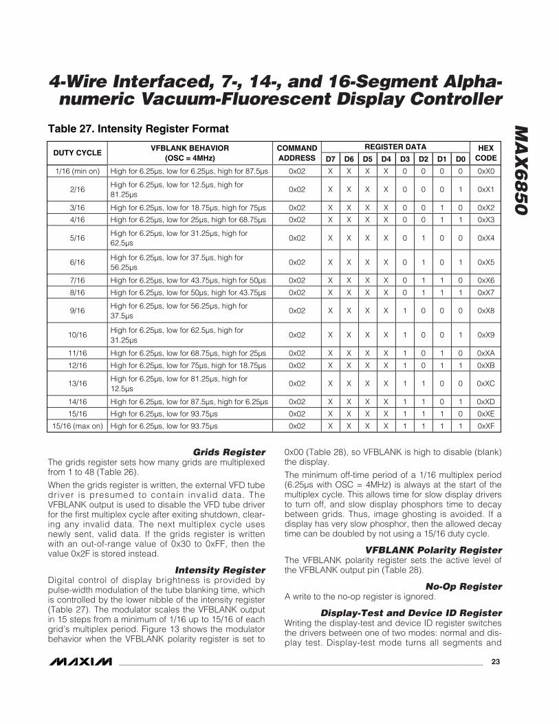
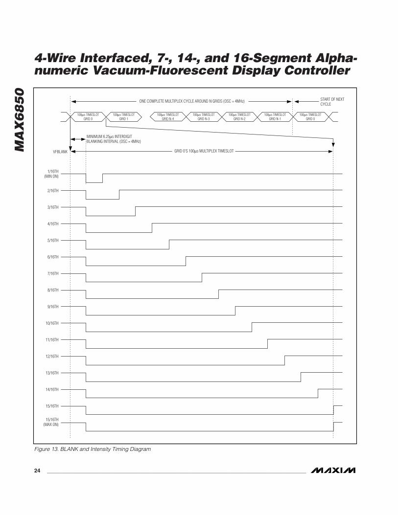
Intensity RegisterDigital control of display brightness is provided bypulse-width modulation of the tube blanking time, whichis controlled by the lower nibble of the intensity register(Table 27). The modulator scales the VFBLANK outputin 15 steps from a minimum of 1/16 up to 15/16 of eachgrid’s multiplex period. Figure 13 shows the modulatorbehavior when the VFBLANK polarity register is set to
0x00 (Table 28), so VFBLANK is high to disable (blank)the display.
The minimum off-time period of a 1/16 multiplex period(6.25µs with OSC = 4MHz) is always at the start of themultiplex cycle. This allows time for slow display driversto turn off, and slow display phosphors time to decaybetween grids. Thus, image ghosting is avoided. If adisplay has very slow phosphor, then the allowed decaytime can be doubled by not using a 15/16 duty cycle.
VFBLANK Polarity RegisterThe VFBLANK polarity register sets the active level ofthe VFBLANK output pin (Table 28).
No-Op RegisterA write to the no-op register is ignored.
Display-Test and Device ID RegisterWriting the display-test and device ID register switchesthe drivers between one of two modes: normal and dis-play test. Display-test mode turns all segments and
MA
X6
85
0
4-Wire Interfaced, 7-, 14-, and 16-Segment Alpha-numeric Vacuum-Fluorescent Display Controller
______________________________________________________________________________________ 23
REGISTER DATADUTY CYCLE
VFBLANK BEHAVIOR(OSC = 4MHz)
COMMANDADDRESS D7 D6 D5 D4 D3 D2 D1 D0
HEXCODE
1/16 (min on) High for 6.25µs, low for 6.25µs, high for 87.5µs 0x02 X X X X 0 0 0 0 0xX0
2/16High for 6.25µs, low for 12.5µs, high for81.25µs
0x02 X X X X 0 0 0 1 0xX1
3/16 High for 6.25µs, low for 18.75µs, high for 75µs 0x02 X X X X 0 0 1 0 0xX2
4/16 High for 6.25µs, low for 25µs, high for 68.75µs 0x02 X X X X 0 0 1 1 0xX3
5/16High for 6.25µs, low for 31.25µs, high for62.5µs
0x02 X X X X 0 1 0 0 0xX4
6/16High for 6.25µs, low for 37.5µs, high for56.25µs
0x02 X X X X 0 1 0 1 0xX5
7/16 High for 6.25µs, low for 43.75µs, high for 50µs 0x02 X X X X 0 1 1 0 0xX6
8/16 High for 6.25µs, low for 50µs, high for 43.75µs 0x02 X X X X 0 1 1 1 0xX7
9/16High for 6.25µs, low for 56.25µs, high for37.5µs
0x02 X X X X 1 0 0 0 0xX8
10/16High for 6.25µs, low for 62.5µs, high for31.25µs
0x02 X X X X 1 0 0 1 0xX9
11/16 High for 6.25µs, low for 68.75µs, high for 25µs 0x02 X X X X 1 0 1 0 0xXA
12/16 High for 6.25µs, low for 75µs, high for 18.75µs 0x02 X X X X 1 0 1 1 0xXB
13/16High for 6.25µs, low for 81.25µs, high for12.5µs
0x02 X X X X 1 1 0 0 0xXC
14/16 High for 6.25µs, low for 87.5µs, high for 6.25µs 0x02 X X X X 1 1 0 1 0xXD
15/16 High for 6.25µs, low for 93.75µs 0x02 X X X X 1 1 1 0 0xXE
15/16 (max on) High for 6.25µs, low for 93.75µs 0x02 X X X X 1 1 1 1 0xXF
Table 27. Intensity Register Format
MA
X6
85
0
4-Wire Interfaced, 7-, 14-, and 16-Segment Alpha-numeric Vacuum-Fluorescent Display Controller
24 ______________________________________________________________________________________
GRID 0'S 100µs MULTIPLEX TIMESLOT
ONE COMPLETE MULTIPLEX CYCLE AROUND N GRIDS (OSC = 4MHz) START OF NEXTCYCLE
100µs TIMESLOTGRID 0
100µs TIMESLOTGRID 1
100µs TIMESLOTGRID N-4
100µs TIMESLOTGRID N-3
100µs TIMESLOTGRID N-2
100µs TIMESLOTGRID N-1
100µs TIMESLOTGRID 0
MINIMUM 6.25µs INTERDIGITBLANKING INTERVAL (OSC = 4MHz)
VFBLANK
1/16TH(MIN ON)
2/16TH
3/16TH
4/16TH
5/16TH
6/16TH
7/16TH
8/16TH
9/16TH
10/16TH
11/16TH
12/16TH
13/16TH
14/16TH
15/16TH
15/16TH(MAX ON)
Figure 13. BLANK and Intensity Timing Diagram
annunciators on and sets the duty cycle to 7/16 (half-power) (Table 29).
Reading the display-test and device ID register returnsthe MAX6850 device ID 0b0000 010 that identifies thedriver type, plus the display-test status in the LSB.
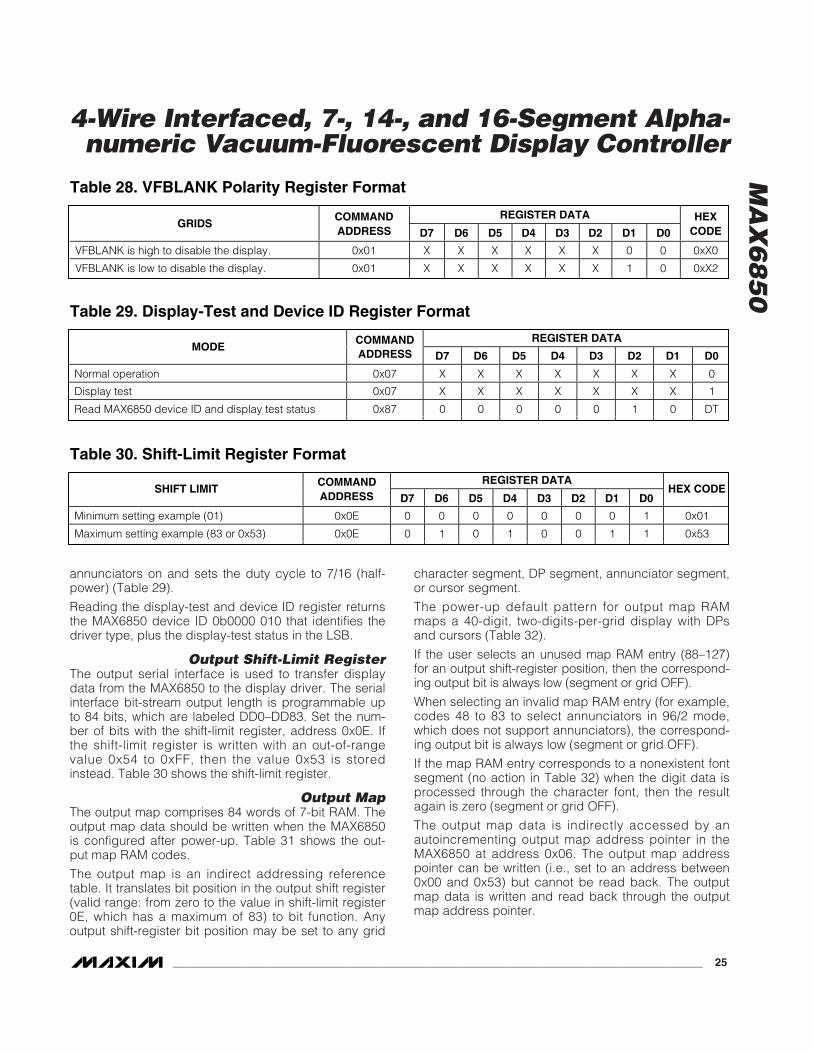
Output Shift-Limit RegisterThe output serial interface is used to transfer displaydata from the MAX6850 to the display driver. The serialinterface bit-stream output length is programmable upto 84 bits, which are labeled DD0–DD83. Set the num-ber of bits with the shift-limit register, address 0x0E. Ifthe shift-limit register is written with an out-of-rangevalue 0x54 to 0xFF, then the value 0x53 is storedinstead. Table 30 shows the shift-limit register.
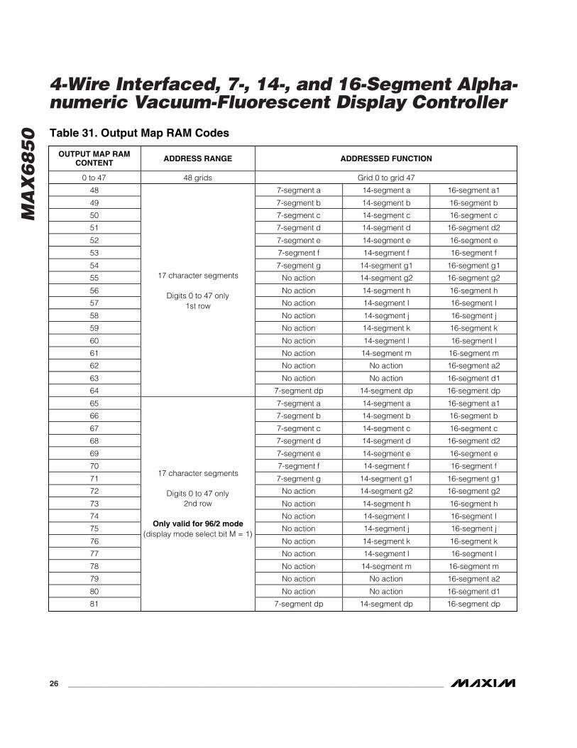
Output MapThe output map comprises 84 words of 7-bit RAM. Theoutput map data should be written when the MAX6850is configured after power-up. Table 31 shows the out-put map RAM codes.
The output map is an indirect addressing referencetable. It translates bit position in the output shift register(valid range: from zero to the value in shift-limit register0E, which has a maximum of 83) to bit function. Anyoutput shift-register bit position may be set to any grid
character segment, DP segment, annunciator segment,or cursor segment.
The power-up default pattern for output map RAMmaps a 40-digit, two-digits-per-grid display with DPsand cursors (Table 32).
If the user selects an unused map RAM entry (88–127)for an output shift-register position, then the correspond-ing output bit is always low (segment or grid OFF).
When selecting an invalid map RAM entry (for example,codes 48 to 83 to select annunciators in 96/2 mode,which does not support annunciators), the correspond-ing output bit is always low (segment or grid OFF).
If the map RAM entry corresponds to a nonexistent fontsegment (no action in Table 32) when the digit data isprocessed through the character font, then the resultagain is zero (segment or grid OFF).
The output map data is indirectly accessed by anautoincrementing output map address pointer in theMAX6850 at address 0x06. The output map addresspointer can be written (i.e., set to an address between0x00 and 0x53) but cannot be read back. The outputmap data is written and read back through the outputmap address pointer.
MA
X6
85
0
4-Wire Interfaced, 7-, 14-, and 16-Segment Alpha-numeric Vacuum-Fluorescent Display Controller
______________________________________________________________________________________ 25
REGISTER DATAGRIDS
COMMANDADDRESS D7 D6 D5 D4 D3 D2 D1 D0
HEXCODE
VFBLANK is high to disable the display. 0x01 X X X X X X 0 0 0xX0
VFBLANK is low to disable the display. 0x01 X X X X X X 1 0 0xX2
Table 28. VFBLANK Polarity Register Format
REGISTER DATAMODE
COMMANDADDRESS D7 D6 D5 D4 D3 D2 D1 D0
Normal operation 0x07 X X X X X X X 0
Display test 0x07 X X X X X X X 1
Read MAX6850 device ID and display test status 0x87 0 0 0 0 0 1 0 DT
Table 29. Display-Test and Device ID Register Format
REGISTER DATASHIFT LIMIT
COMMANDADDRESS D7 D6 D5 D4 D3 D2 D1 D0
HEX CODE
Minimum setting example (01) 0x0E 0 0 0 0 0 0 0 1 0x01
Maximum setting example (83 or 0x53) 0x0E 0 1 0 1 0 0 1 1 0x53
Table 30. Shift-Limit Register Format
MA
X6
85
0
4-Wire Interfaced, 7-, 14-, and 16-Segment Alpha-numeric Vacuum-Fluorescent Display Controller
26 ______________________________________________________________________________________
OUTPUT MAP RAMCONTENT ADDRESS RANGE ADDRESSED FUNCTION
0 to 47 48 grids Grid 0 to grid 47
48 7-segment a 14-segment a 16-segment a1
49 7-segment b 14-segment b 16-segment b
50 7-segment c 14-segment c 16-segment c
51 7-segment d 14-segment d 16-segment d2
52 7-segment e 14-segment e 16-segment e
53 7-segment f 14-segment f 16-segment f
54 7-segment g 14-segment g1 16-segment g1
55 No action 14-segment g2 16-segment g2
56 No action 14-segment h 16-segment h
57 No action 14-segment I 16-segment I
58 No action 14-segment j 16-segment j
59 No action 14-segment k 16-segment k
60 No action 14-segment l 16-segment l
61 No action 14-segment m 16-segment m
62 No action No action 16-segment a2
63 No action No action 16-segment d1
64
17 character segments
Digits 0 to 47 only1st row
7-segment dp 14-segment dp 16-segment dp
65 7-segment a 14-segment a 16-segment a1
66 7-segment b 14-segment b 16-segment b
67 7-segment c 14-segment c 16-segment c
68 7-segment d 14-segment d 16-segment d2
69 7-segment e 14-segment e 16-segment e
70 7-segment f 14-segment f 16-segment f
71 7-segment g 14-segment g1 16-segment g1
72 No action 14-segment g2 16-segment g2
73 No action 14-segment h 16-segment h
74 No action 14-segment I 16-segment I
75 No action 14-segment j 16-segment j
76 No action 14-segment k 16-segment k
77 No action 14-segment l 16-segment l
78 No action 14-segment m 16-segment m
79 No action No action 16-segment a2
80 No action No action 16-segment d1
81
17 character segments
Digits 0 to 47 only2nd row
Only valid for 96/2 mode(display mode select bit M = 1)
7-segment dp 14-segment dp 16-segment dp
Table 31. Output Map RAM Codes
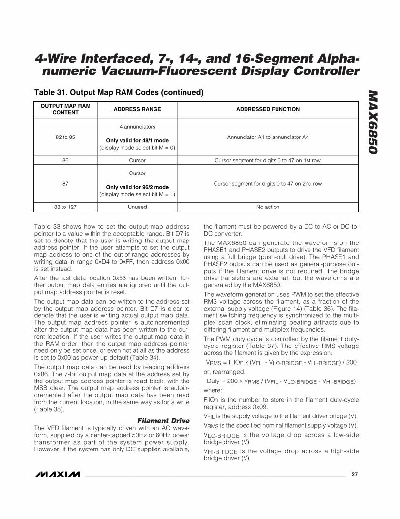
Table 33 shows how to set the output map addresspointer to a value within the acceptable range. Bit D7 isset to denote that the user is writing the output mapaddress pointer. If the user attempts to set the outputmap address to one of the out-of-range addresses bywriting data in range 0xD4 to 0xFF, then address 0x00is set instead.
After the last data location 0x53 has been written, fur-ther output map data entries are ignored until the out-put map address pointer is reset.
The output map data can be written to the address setby the output map address pointer. Bit D7 is clear todenote that the user is writing actual output map data.The output map address pointer is autoincrementedafter the output map data has been written to the cur-rent location. If the user writes the output map data inthe RAM order, then the output map address pointerneed only be set once, or even not at all as the addressis set to 0x00 as power-up default (Table 34).
The output map data can be read by reading address0x86. The 7-bit output map data at the address set bythe output map address pointer is read back, with theMSB clear. The output map address pointer is autoin-cremented after the output map data has been readfrom the current location, in the same way as for a write(Table 35).
Filament DriveThe VFD filament is typically driven with an AC wave-form, supplied by a center-tapped 50Hz or 60Hz powertransformer as part of the system power supply.However, if the system has only DC supplies available,
the filament must be powered by a DC-to-AC or DC-to-DC converter.
The MAX6850 can generate the waveforms on thePHASE1 and PHASE2 outputs to drive the VFD filamentusing a full bridge (push-pull drive). The PHASE1 andPHASE2 outputs can be used as general-purpose out-puts if the filament drive is not required. The bridgedrive transistors are external, but the waveforms aregenerated by the MAX6850.
The waveform generation uses PWM to set the effectiveRMS voltage across the filament, as a fraction of theexternal supply voltage (Figure 14) (Table 36). The fila-ment switching frequency is synchronized to the multi-plex scan clock, eliminating beating artifacts due todiffering filament and multiplex frequencies.
The PWM duty cycle is controlled by the filament duty-cycle register (Table 37). The effective RMS voltageacross the filament is given by the expression:
VRMS = FilOn x (VFIL - VLO-BRIDGE - VHI-BRIDGE) / 200
or, rearranged:
Duty = 200 x VRMS / (VFIL - VLO-BRIDGE - VHI-BRIDGE)
where:
FilOn is the number to store in the filament duty-cycleregister, address 0x09.
VFIL is the supply voltage to the filament driver bridge (V).
VRMS is the specified nominal filament supply voltage (V).
VLO-BRIDGE is the voltage drop across a low-sidebridge driver (V).
VHI-BRIDGE is the voltage drop across a high-sidebridge driver (V).
MA
X6
85
0
4-Wire Interfaced, 7-, 14-, and 16-Segment Alpha-numeric Vacuum-Fluorescent Display Controller
______________________________________________________________________________________ 27
OUTPUT MAP RAMCONTENT ADDRESS RANGE ADDRESSED FUNCTION
82 to 85
4 annunciators
Only valid for 48/1 mode(display mode select bit M = 0)
Annunciator A1 to annunciator A4
86 Cursor Cursor segment for digits 0 to 47 on 1st row
87
Cursor
Only valid for 96/2 mode(display mode select bit M = 1)
Cursor segment for digits 0 to 47 on 2nd row
88 to 127 Unused No action
Table 31. Output Map RAM Codes (continued)

MA
X6
85
0
4-Wire Interfaced, 7-, 14-, and 16-Segment Alpha-numeric Vacuum-Fluorescent Display Controller
28 ______________________________________________________________________________________
OUTPUT MAP RAMADDRESS
POWER-UP DEFAULTCONTENT ADDRESSED FUNCTION
0 to 39 0 to 39 (in order) Grid 0 to grid 39
40 48 7-segment a 14-segment a 16-segment a1
41 49 7-segment b 14-segment b 16-segment b
42 50 7-segment c 14-segment c 16-segment c
43 51 7-segment d 14-segment d 16-segment d2
44 52 7-segment e 14-segment e 16-segment e
45 53 7-segment f 14-segment f 16-segment f
46 54 7-segment g 14-segment g1 16-segment g1
47 55 No action 14-segment g2 16-segment g2
48 56 No action 14-segment h 16-segment h
49 57 No action 14-segment I 16-segment I
50 58 No action 14-segment j 16-segment j
51 59 No action 14-segment k 16-segment k
52 60 No action 14-segment l 16-segment l
53 61 No action 14-segment m 16-segment m
54 62 No action No action 16-segment a2
55 63 No action No action 16-segment d2
56 64 7-segment dp 14-segment dp 16-segment dp
57 65 7-segment a 14-segment a 16-segment a1
58 66 7-segment b 14-segment b 16-segment b
59 67 7-segment c 14-segment c 16-segment c
60 68 7-segment d 14-segment d 16-segment d1
61 69 7-segment e 14-segment e 16-segment e
62 70 7-segment f 14-segment f 16-segment f
63 71 7-segment g 14-segment g1 16-segment g1
64 72 No action 14-segment g2 16-segment g2
65 73 No action 14-segment h 16-segment h
66 74 No action 14-segment I 16-segment I
67 75 No action 14-segment j 16-segment j
68 76 No action 14-segment k 16-segment k
69 77 No action 14-segment l 16-segment l
70 78 No action 14-segment m 16-segment m
71 79 No action No action 16-segment a2
72 80 No action No action 16-segment d1
73 81 7-segment dp 14-segment dp 16-segment dp
74 86 (Note: Value is not 82.) Cursor segment for digits 0 to 47 1st row
75 87 (Note: Value is not 83.) Cursor segment for digits 0 to 47 2nd row
76 to 83 127 No action
Table 32. Output Map RAM Initial Power-Up Status
MA
X6
85
0
4-Wire Interfaced, 7-, 14-, and 16-Segment Alpha-numeric Vacuum-Fluorescent Display Controller
______________________________________________________________________________________ 29
Table 35. Reading Output Map Data
REGISTER DATAMODE
COMMANDADDRESS D7 D6 D5 D4 D3 D2 D1 D0
Read output map data; output map address pointer isautoincremented after the output map data has beenread from the current location.
0x86 0 7 bits of output map data
TIMING POINT PHASE1 BEHAVIOR PHASE2 BEHAVIOREXAMPLE 1
DUTY = 1 (MIN)EXAMPLE 2DUTY = 100
EXAMPLE 3DUTY = 198
(A)Low for (199 - FilOn)
cyclesLow for (199 - FilOn)
cycles198 99 1
(B) Low for (FilOn) cycles High for (FilOn) cycles 1 100 198
(C) Low for (2) cycles Low for (2) cycles 2 2 2
(D) High for (FilOn) cycles Low for (FilOn) cycles 1 100 198
(E)Low for (199 - FilOn)
cyclesLow for (199 - FilOn)
cycles198 99 1
Total 4MHzcycles
(OSC = 4MHz)400 cycles = 100µs 400 cycles = 100µs
400 cycles =100µs
400 cycles =100µs
400 cycles =100µs
Table 36. Filament Bridge Driver Timing
REGISTER DATAMODE
COMMANDADDRESS D7 D6 D5 D4 D3 D2 D1 D0
Set output map address to minimum (0x00) with data0x80. (Note that this address is set as a power-updefault.)
0x06 1 0 0 0 0 0 0 0
Set output map address to maximum 0x53 with data0xD3.
0x06 1 1 1 1 1 0 0 1
Table 33. Setting Output Map Address Pointer
REGISTER DATAMODE
COMMANDADDRESS D7 D6 D5 D4 D3 D2 D1 D0
Write output map data; output map address pointer isautoincremented after the output map data has beenwritten to the current location.
0x06 0 7 bits of output map data
Table 34. Writing Output Map Data

MA
X6
85
0
The minimum commutation time, shown at (C) in Figure14, is set by (2/OSC)s (500ns when OSC = 4MHz) toensure that shoot-through currents cannot flow duringphase reversal. Otherwise, the duty cycle of the bridge(total on time: total time) sets the RMS voltage acrossthe filament. This technique provides a low-cost AC fila-ment supply when using a regulated supply higher thanthe RMS voltage rating of the filament.
Figure 15 shows the external components required forthe filament driver using a FET bridge.
PHASE1 and PHASE2 OutputsPHASE1 and PHASE2 can be individually programmedas one of four output types (Tables 38, 39).
When using the filament drive, first ensure that the fila-ment duty-cycle register 0x09 is set to the correct valuebefore configuring the PHASE1 and PHASE2 outputs to
be filament drives. To stop the filament drive, programeither PHASE1 or PHASE2 (or both) to be logic-low gen-eral-purpose outputs. Both PHASE1 and PHASE2 out-puts come out of power-on-reset in logic-low condition.
PUMP OutputThe PUMP output can be programmed as one of fouroutput types (Table 40).
PORT0 and PORT1 OutputsPORT0 and PORT1 can be individually programmed asone of eight output types (Tables 41, 42). The PORT1choices are similar to the PORT0 choices, except thatthe last four items are invert logic. PORT0 output comesout of power-on-reset in logic-low condition, whereasPORT1 output initializes high.
The PORT0 and PORT1 shutdown outputs allow exter-nal hardware (for example, a DC-DC converter powersupply for VFD) to be disabled by the MAX6850 whenthe MAX6850 is shut down.
The 625Hz, 1250Hz, and 2500Hz outputs can drive apiezo sounder either from PORT0 or PORT1 alone, orby both ports together as bridge drive. For bridgedrive, the sounder is connected between PORT0 andPORT1, taking advantage of the PORT1 output beinginverted with respect to PORT0. Select different fre-quencies for PORT0 and PORT1 to obtain a widerrange of sounds when bridge drive is used.
Multiplex Clock and Blink TimingThe OSC1 and OSC2 inputs set the multiplex and blinktiming for the display driver. Connect an external resis-tor from OSC2 to GND and an external capacitor COSCfrom OSC1 to GND to set the frequency of the internalRC oscillator. Alternatively, overdrive OSC1 with anexternal TTL or CMOS clock. If an exact blink rate ormultiplex period is required, use an external clockranging between 2MHz and 8MHz to drive OSC1.
The multiplex clock frequency determines the multiplexscan rate and the blink timing. The display scan rate isOSC / 400 / (1 + grids register value). There are 400OSC cycles per digit multiplex period. For example,with OSC = 4MHz, each display digit is enabled for100µs. For a 40-grid display tube (grids register value= 39 or 0x27), the display scan rate is 250Hz.
4-Wire Interfaced, 7-, 14-, and 16-Segment Alpha-numeric Vacuum-Fluorescent Display Controller
30 ______________________________________________________________________________________
(A)(B)
(C) (D)(E)
100µs MULTIPLEX TIME PERIOD (OSC = 4MHz)
PHASE 1
PHASE 2
Figure 14. Filament Bridge Driver Timing Waveforms
R2 R4Q2
Q1
GND
Q3
Q4
PHASE 1
PHASE 2
VFIL
VFD TUBE
GND
Figure 15. Filament Bridge Driver (MOSFET)
REGISTER DATAFILAMENT DUTY CYCLE
COMMANDADDRESS D7 D6 D5 D4 D3 D2 D1 D0
HEX CODE
Minimum setting example (01) 0x09 0 0 0 0 0 0 0 1 0x01
Maximum setting example (199 or 0xC7) 0x09 1 1 0 0 0 1 1 1 0xC7
Table 37. Filament Duty-Cycle Register Format
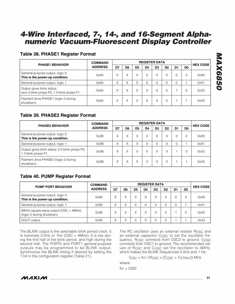
The BLINK output is the selectable blink period clock. Itis nominally 0.5Hz or 1Hz (OSC = 4MHz). It is low dur-ing the first half of the blink period, and high during thesecond half. The PORT0 and PORT1 general-purposeoutputs may be programmed to be BLINK output.Synchronize the BLINK timing if desired by setting theT bit in the configuration register (Table 21).
The RC oscillator uses an external resistor ROSC andan external capacitor COSC to set the oscillator fre-quency. ROSC connects from OSC2 to ground. COSCconnects from OSC1 to ground. The recommended val-ues of ROSC and COSC set the oscillator to 4MHz,which makes the BLINK frequencies 0.5Hz and 1 Hz:
fOSC = KF / (ROSC x [COSC + CSTRAY]) MHz
where:
KF = 2320
MA
X6
85
0
4-Wire Interfaced, 7-, 14-, and 16-Segment Alpha-numeric Vacuum-Fluorescent Display Controller
______________________________________________________________________________________ 31
Table 38. PHASE1 Register Format
REGISTER DATAPHASE1 BEHAVIOR
COMMANDADDRESS D7 D6 D5 D4 D3 D2 D1 D0
HEX CODE
General-purpose output, logic 0.This is the power-up condition.
0x0A X X X X X X 0 0 0xX0
General-purpose output, logic 1. 0x0A X X X X X X 0 1 0xX1
Output gives blink status:zero if blink phase P0; 1 if blink phase P1.
0x0A X X X X X X 1 0 0xX2
Filament drive PHASE1 (logic 0 duringshutdown).
0x0A X X X X X X 1 1 0xX3
REGISTER DATAPHASE2 BEHAVIOR
COMMANDADDRESS D7 D6 D5 D4 D3 D2 D1 D0
HEX CODE
General-purpose output, logic 0.This is the power-up condition.
0x0B X X X X X X 0 0 0xX0
General-purpose output, logic 1. 0x0B X X X X X X 0 1 0xX1
Output gives blink status: 0 if blink phase P0;1 if blink phase P1.
0x0B X X X X X X 1 0 0xX2
Filament drive PHASE2 (logic 0 duringshutdown).
0x0B X X X X X X 1 1 0xX3
Table 39. PHASE2 Register Format
REGISTER DATAPUMP PORT BEHAVIOR
COMMANDADDRESS D7 D6 D5 D4 D3 D2 D1 D0
HEX CODE
General-purpose output, logic 0.This is the power-up condition.
0x08 X X X X X X 0 0 0xX0
General-purpose output, logic 1. 0x08 X X X X X X 0 1 0xX1
80kHz square-wave output (OSC = 4MHz)(logic 0 during shutdown).
0x08 X X X X X X 1 0 0xX2
DOUT output. 0x08 X X X X X X 1 1 0xX3
Table 40. PUMP Register Format
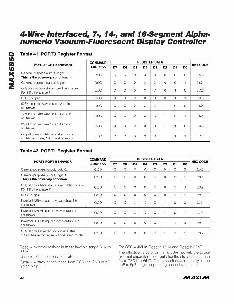
MA
X6
85
0
ROSC = external resistor in kΩ (allowable range 8kΩ to80kΩ)
COSC = external capacitor in pF
CSTRAY = stray capacitance from OSC1 to GND in pF,typically 2pF
For OSC = 4MHz, ROSC is 10kΩ and COSC is 56pF.
The effective value of COSC includes not only the actualexternal capacitor used, but also the stray capacitancefrom OSC1 to GND. This capacitance is usually in the1pF to 5pF range, depending on the layout used.
4-Wire Interfaced, 7-, 14-, and 16-Segment Alpha-numeric Vacuum-Fluorescent Display Controller
32 ______________________________________________________________________________________
REGISTER DATAPORT0 PORT BEHAVIOR
COMMANDADDRESS D7 D6 D5 D4 D3 D2 D1 D0
HEX CODE
General-purpose output, logic 0.This is the power-up condition.
0x0C X X X X X 0 0 0 0xX0
General-purpose output, logic 1. 0x0C X X X X X 0 0 1 0xX1
Outp ut g i ves b l i nk status: zer o i f b l i nk p haseP 0; 1 if blink phase P1.
0x0C X X X X X 0 1 0 0xX2
DOUT output. 0x0C X X X X X 0 1 1 0xX3
625Hz square-wave output zero inshutdown.
0x0C X X X X X 1 0 0 0xX4
1250Hz square-wave output zero inshutdown.
0x0C X X X X X 1 0 1 0xX5
2500Hz square-wave output zero inshutdown.
0x0C X X X X X 1 1 0 0xX6
Output gives shutdown status: zero ifshutdown mode; 1 if operating mode.
0x0C X X X X X 1 1 1 0xX7
Table 41. PORT0 Register Format
REGISTER DATAPORT1 PORT BEHAVIOR
COMMANDADDRESS D7 D6 D5 D4 D3 D2 D1 D0
HEX CODE
General-purpose output, logic 0. 0x0D X X X X X 0 0 0 0xX0
General-purpose output, logic 1.This is the power-up condition.
0x0D X X X X X 0 0 1 0xX1
Output gives blink status: zero if blink phaseP0; 1 if blink phase P1.
0x0D X X X X X 0 1 0 0xX2
DOUT output. 0x0D X X X X X 0 1 1 0xX3
Inverted 625Hz square-wave output 1 inshutdown.
0x0D X X X X X 1 0 0 0xX4
Inverted 1250Hz square-wave output 1 inshutdown.
0x0D X X X X X 1 0 1 0xX5
Inverted 2500Hz square-wave output 1 inshutdown.
0x0D X X X X X 1 1 0 0xX6
Output gives inverted shutdown status:1 if shutdown mode; zero if operating mode.
0x0D X X X X X 1 1 1 0xX7
Table 42. PORT1 Register Format
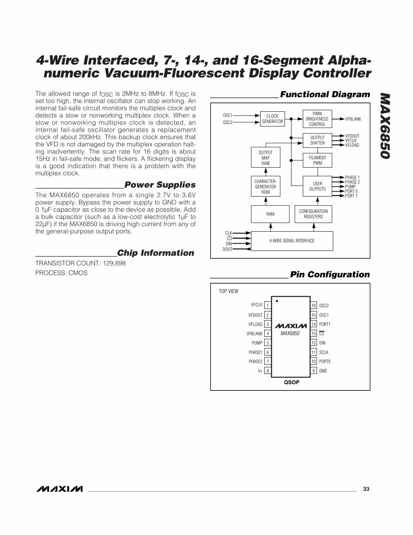
The allowed range of fOSC is 2MHz to 8MHz. If fOSC isset too high, the internal oscillator can stop working. Aninternal fail-safe circuit monitors the multiplex clock anddetects a slow or nonworking multiplex clock. When aslow or nonworking multiplex clock is detected, aninternal fail-safe oscillator generates a replacementclock of about 200kHz. This backup clock ensures thatthe VFD is not damaged by the multiplex operation halt-ing inadvertently. The scan rate for 16 digits is about15Hz in fail-safe mode, and flickers. A flickering displayis a good indication that there is a problem with themultiplex clock.
Power SuppliesThe MAX6850 operates from a single 2.7V to 3.6Vpower supply. Bypass the power supply to GND with a0.1µF capacitor as close to the device as possible. Adda bulk capacitor (such as a low-cost electrolytic 1µF to22µF) if the MAX6850 is driving high current from any ofthe general-purpose output ports.
Chip InformationTRANSISTOR COUNT: 129,898
PROCESS: CMOS
MA
X6
85
0
4-Wire Interfaced, 7-, 14-, and 16-Segment Alpha-numeric Vacuum-Fluorescent Display Controller
______________________________________________________________________________________ 33
Functional Diagram
OSC1OSC2
VFBLANK
CLKCS
DINDOUT
4-WIRE SERIAL INTERFACE
RAMCONFIGURATION
REGISTERS
CHARACTER-GENERATOR
ROM
OUTPUTMAPRAM
USEROUTPUTS
FILAMENTPWM
CLOCKGENERATOR
PWMBRIGHTNESS
CONTROL
VFCLKVFDOUT
VFLOAD
PHASE 2PHASE 1
PUMPPORT 0PORT 1
OUTPUTSHIFTER
16
15
14
13
12
11
10
9
1
2
3
4
5
6
7
8
VFCLK OSC2
OSC1
PORT1
DIN
SCLK
PORT0
GND
TOP VIEW
MAX6850
VFDOUT
VFLOAD
PHASE1
VFBLANK
PUMP
PHASE2
V+
CS
QSOP
Pin Configuration
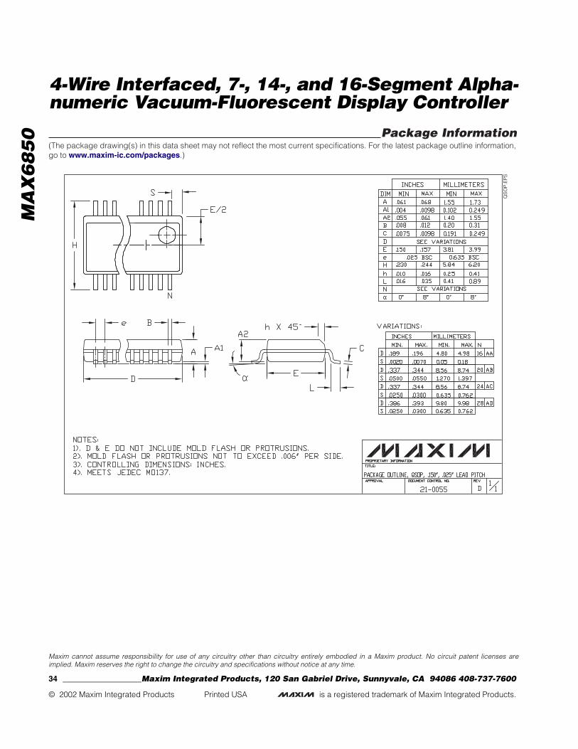
Package Information(The package drawing(s) in this data sheet may not reflect the most current specifications. For the latest package outline information,go to www.maxim-ic.com/packages.)
QS
OP
.EP
S
MA
X6
85
0
4-Wire Interfaced, 7-, 14-, and 16-Segment Alpha-numeric Vacuum-Fluorescent Display Controller
Maxim cannot assume responsibility for use of any circuitry other than circuitry entirely embodied in a Maxim product. No circuit patent licenses areimplied. Maxim reserves the right to change the circuitry and specifications without notice at any time.
34 ____________________Maxim Integrated Products, 120 San Gabriel Drive, Sunnyvale, CA 94086 408-737-7600
© 2002 Maxim Integrated Products Printed USA is a registered trademark of Maxim Integrated Products.