4.0 introduction...emitter coupled astable multivibrator mono stable and bistable multivibrator...
TRANSCRIPT
UNIT IV - MULTIVIBRATOR CIRCUITS:
Collector coupled and complementary collector coupled astable multivibrators —
Emitter coupled astable multivibrator mono stable and bistable multivibrator using
similar and complementary transistors — Triggering methods — Storage delay and
calculation of times Switching — Speed up capacitors Schmitt trigger circuits.
4.0 INTRODUCTION:
A binary circuit can have 2 stable states.
It may remain in one of the.2 stable states permanently.
The mono stable circuit has only 1 permanently stable state and 1 quasi stable
state.
In the mono stable configuration a triggering signal is required to induce a
transition from the stable state to the quasi stable state.
The time for which it stays in the quasi stable state may be very long in
comparison with the time of transition between the states.
It may return to the stable state without any external signal eventually.
The Astable circuit has 2 states both of which are quasi stable it switches from one
stable state to the other without the requirement of any external signal.
Both the above circuits find extensive application in pulse circuitry.
The basic application of the mono stable configuration arises from the fact that it
may be use to establish a fixed time interval the beginning and end of which are
marked by a abrupt discontinuity in a voltage waveform.
A bistable circuit is one that can exist indefinitely in either of the 2 stab states.
It can be induced to make an abrupt transition from one state to another 1 means
of external excitation.
A bistable multi vibrator is used in counting and storing of digital information.
It can also be applied in the generation and processing pulse type waveforms.
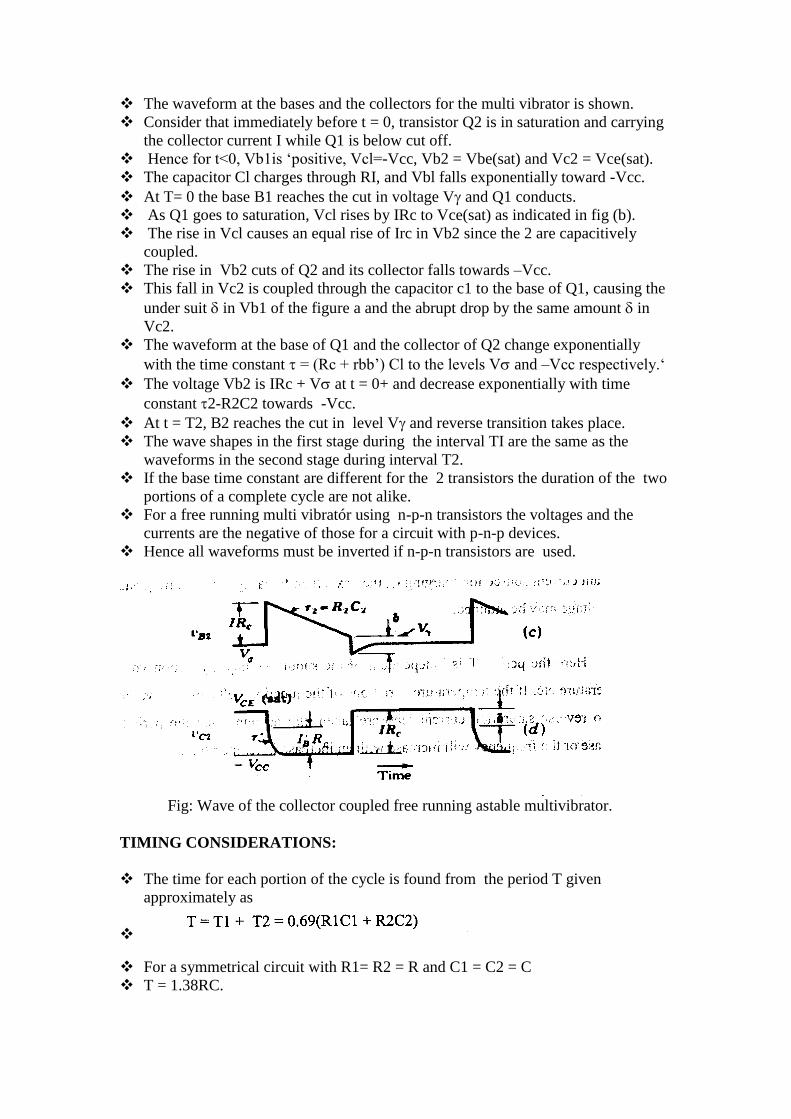
COLLECTOR COUPLED ASTABLE MULTIVIBRATOR:
The circuit shows a PNP collector coupled free running multi vibrator using
transistors.
There exists a capacitive coupling between the stages. So both the transistors
cannot remain at cut off.
The circuit instead has 2 quasi stable states, between which it can make
transitions.
Fig: Collector,çoupled astable multivibrator
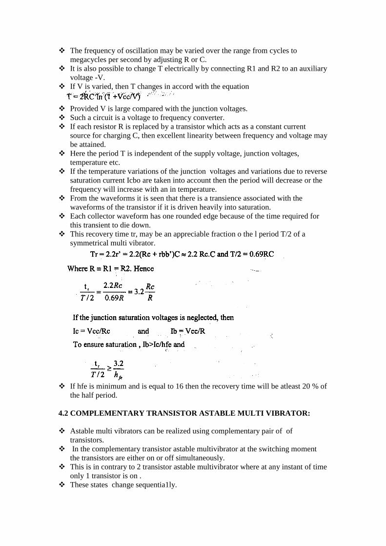
The waveform at the bases and the collectors for the multi vibrator is shown.
Consider that immediately before t = 0, transistor Q2 is in saturation and carrying
the collector current I while Q1 is below cut off.
Hence for t<0, Vb1is ‗positive, Vcl=-Vcc, Vb2 = Vbe(sat) and Vc2 = Vce(sat).
The capacitor Cl charges through RI, and Vbl falls exponentially toward -Vcc.
At T= 0 the base B1 reaches the cut in voltage V and Q1 conducts.
As Q1 goes to saturation, Vcl rises by IRc to Vce(sat) as indicated in fig (b).
The rise in Vcl causes an equal rise of Irc in Vb2 since the 2 are capacitively
coupled.
The rise in Vb2 cuts of Q2 and its collector falls towards –Vcc.
This fall in Vc2 is coupled through the capacitor c1 to the base of Q1, causing the
under suit in Vb1 of the figure a and the abrupt drop by the same amount in
Vc2.
The waveform at the base of Q1 and the collector of Q2 change exponentially
with the time constant = (Rc + rbb‘) Cl to the levels V and –Vcc respectively.‗
The voltage Vb2 is IRc + V at t = 0+ and decrease exponentially with time
constant 2-R2C2 towards -Vcc.
At t = T2, B2 reaches the cut in level V and reverse transition takes place.
The wave shapes in the first stage during the interval TI are the same as the
waveforms in the second stage during interval T2.
If the base time constant are different for the 2 transistors the duration of the two
portions of a complete cycle are not alike.
For a free running multi vibratór using n-p-n transistors the voltages and the
currents are the negative of those for a circuit with p-n-p devices.
Hence all waveforms must be inverted if n-p-n transistors are used.
Fig: Wave of the collector coupled free running astable multivibrator.
TIMING CONSIDERATIONS:
The time for each portion of the cycle is found from the period T given
approximately as
For a symmetrical circuit with R1= R2 = R and C1 = C2 = C
T = 1.38RC.
The frequency of oscillation may be varied over the range from cycles to
megacycles per second by adjusting R or C.
It is also possible to change T electrically by connecting R1 and R2 to an auxiliary
voltage -V.
If V is varied, then T changes in accord with the equation
Provided V is large compared with the junction voltages.
Such a circuit is a voltage to frequency converter.
If each resistor R is replaced by a transistor which acts as a constant current
source for charging C, then excellent linearity between frequency and voltage may
be attained.
Here the period T is independent of the supply voltage, junction voltages,
temperature etc.
If the temperature variations of the junction voltages and variations due to reverse
saturation current Icbo are taken into account then the period will decrease or the
frequency will increase with an in temperature.
From the waveforms it is seen that there is a transience associated with the
waveforms of the transistor if it is driven heavily into saturation.
Each collector waveform has one rounded edge because of the time required for
this transient to die down.
This recovery time tr, may be an appreciable fraction o the l period T/2 of a
symmetrical multi vibrator.
If hfe is minimum and is equal to 16 then the recovery time will be atleast 20 % of
the half period.
4.2 COMPLEMENTARY TRANSISTOR ASTABLE MULTI VIBRATOR:
Astable multi vibrators can be realized using complementary pair of of
transistors.
In the complementary transistor astable multivibrator at the switching moment
the transistors are either on or off simultaneously.
This is in contrary to 2 transistor astable multivibrator where at any instant of time
only 1 transistor is on .
These states change sequentia1ly.
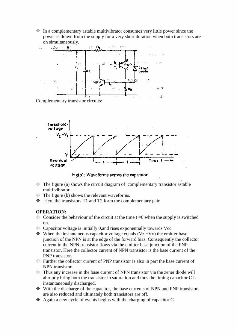
In a complementary astable multivibrator consumes very little power since the
power is drawn from the supply for a very short duration when both transistors are
on simultaneously.
Complementary transistor circuits:
The figure (a) shows the circuit diagram of complementary transistor astable
multi vibrator.
The figure (b) shows the relevant waveforms.
Here the transistors T1 and T2 form the complementary pair.
OPERATION:
Consider the behaviour of the circuit at the time t =0 when the supply is switched
on.
Capacitor voltage is initially 0,and rises exponentially towards Vcc.
When the instantaneous capacitor voltage equals (Vz +Vv) the emitter base
junction of the NPN is at the edge of the forward bias. Consequently the collector
current in the NPN transistor flows via the emitter base junction of the PNP
transistor. Here the collector current of NPN transistor is the base current of the
PNP transistor.
Further the collector current of PNP transistor is also in part the base current of
NPN transistor.
Thus any increase in the base current of NPN transistor via the zener diode will
abruptly bring both the transistor in saturation and thus the timing capacitor C is
instantaneously discharged.
With the discharge of the capacitor, the base currents of NPN and PNP transistors
are also reduced and ultimately both transistors are off.
Again a new cycle of events begins with the charging of capacitor C.
If Vi is the residual voltage across the capacitor, when the switch is off, it can be
shown that the expression for repetition is
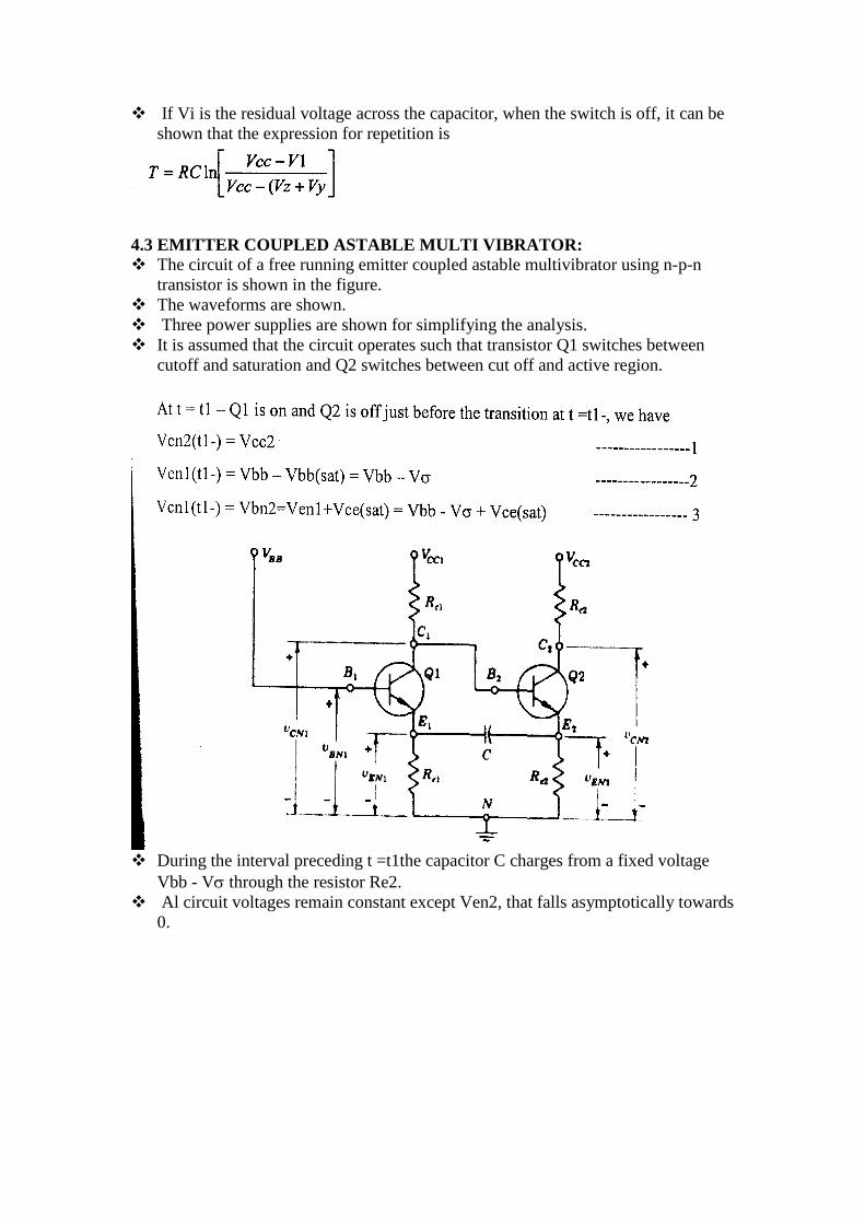
4.3 EMITTER COUPLED ASTABLE MULTI VIBRATOR:
The circuit of a free running emitter coupled astable multivibrator using n-p-n
transistor is shown in the figure.
The waveforms are shown.
Three power supplies are shown for simplifying the analysis.
It is assumed that the circuit operates such that transistor Q1 switches between
cutoff and saturation and Q2 switches between cut off and active region.
During the interval preceding t =t1the capacitor C charges from a fixed voltage
Vbb - V through the resistor Re2.
Al circuit voltages remain constant except Ven2, that falls asymptotically towards
0.
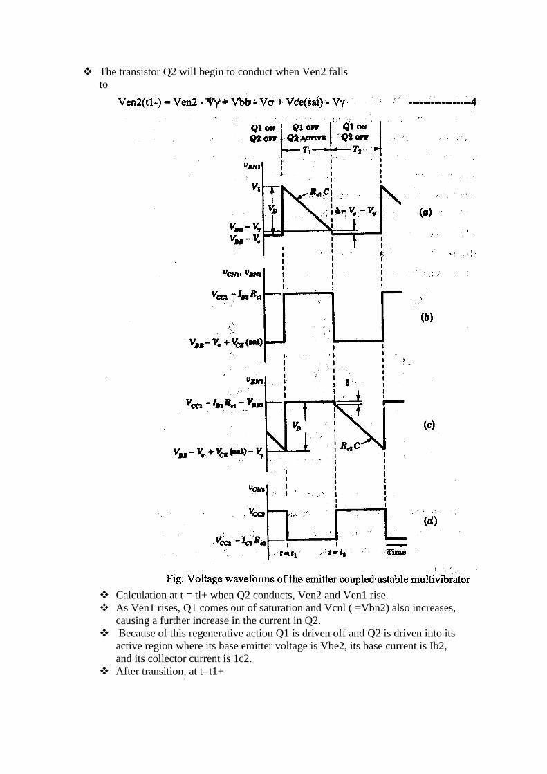
The transistor Q2 will begin to conduct when Ven2 falls
to
Calculation at t = tl+ when Q2 conducts, Ven2 and Ven1 rise.
As Ven1 rises, Q1 comes out of saturation and Vcnl ( =Vbn2) also increases,
causing a further increase in the current in Q2.
Because of this regenerative action Q1 is driven off and Q2 is driven into its
active region where its base emitter voltage is Vbe2, its base current is Ib2,
and its collector current is 1c2.
After transition, at t=t1+
At t1 there is an abrupt change Vd in Ven2 (fig c).
Because of the capacitive coupling between the emitters there must also be the
same discontinuity Vd in Ven1.
Hence
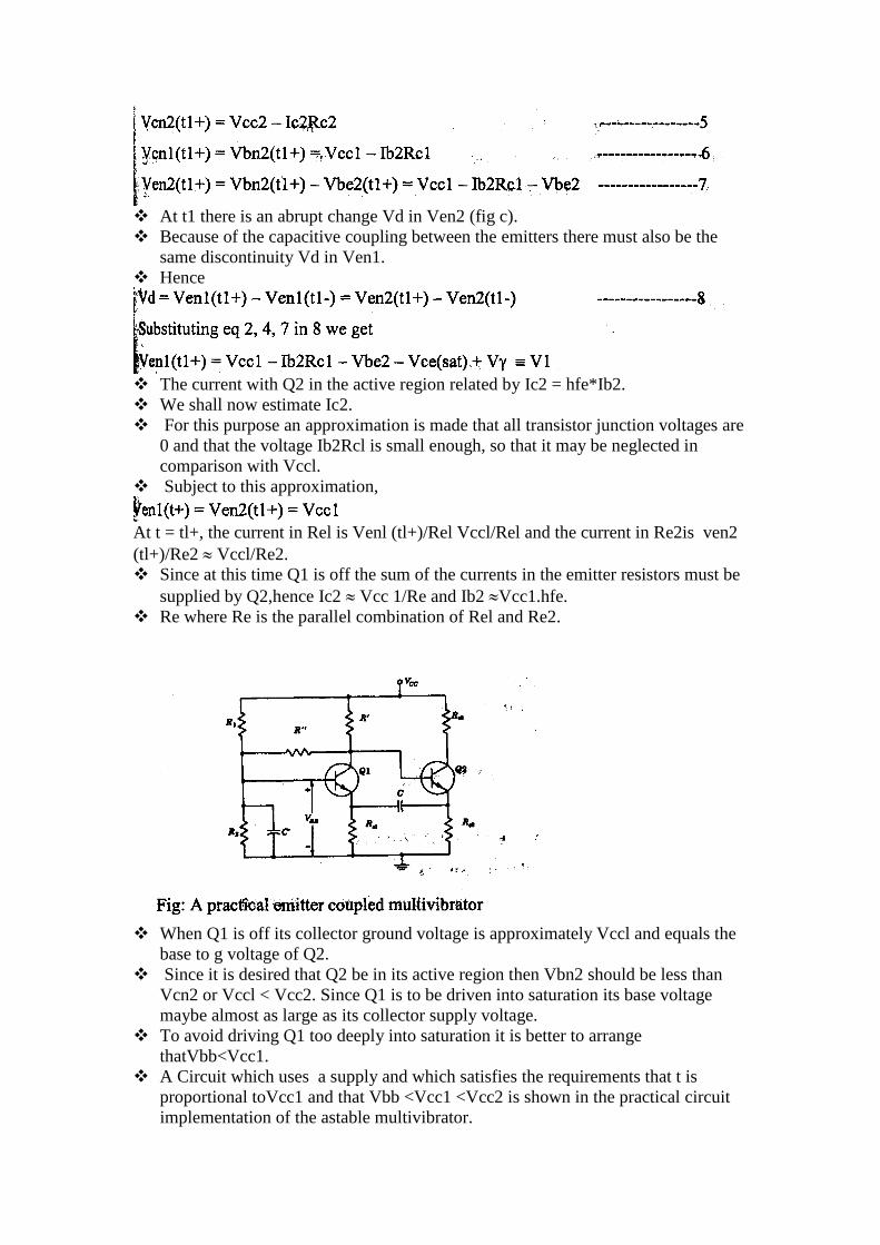
The current with Q2 in the active region related by Ic2 = hfe*Ib2.
We shall now estimate Ic2.
For this purpose an approximation is made that all transistor junction voltages are
0 and that the voltage Ib2Rcl is small enough, so that it may be neglected in
comparison with Vccl.
Subject to this approximation,
At t = tl+, the current in Rel is Venl (tl+)/Rel Vccl/Rel and the current in Re2is ven2
(tl+)/Re2 Vccl/Re2.
Since at this time Q1 is off the sum of the currents in the emitter resistors must be
supplied by Q2,hence Ic2 Vcc 1/Re and Ib2 Vcc1.hfe.
Re where Re is the parallel combination of Rel and Re2.
When Q1 is off its collector ground voltage is approximately Vccl and equals the
base to g voltage of Q2.
Since it is desired that Q2 be in its active region then Vbn2 should be less than
Vcn2 or Vccl < Vcc2. Since Q1 is to be driven into saturation its base voltage
maybe almost as large as its collector supply voltage.
To avoid driving Q1 too deeply into saturation it is better to arrange
thatVbb<Vcc1.
A Circuit which uses a supply and which satisfies the requirements that t is
proportional toVcc1 and that Vbb <Vcc1 <Vcc2 is shown in the practical circuit
implementation of the astable multivibrator.
Since C is a bypass capacitor intended to maintain Vbb constant, it is not
involved in the operation of the circuit.
It s assumed that R1 and R2 are small enough so that the voltage Vbb at the
junction of R1 and R2 remains nominally constant during the entire cycle of
operations of the multi vibrator.
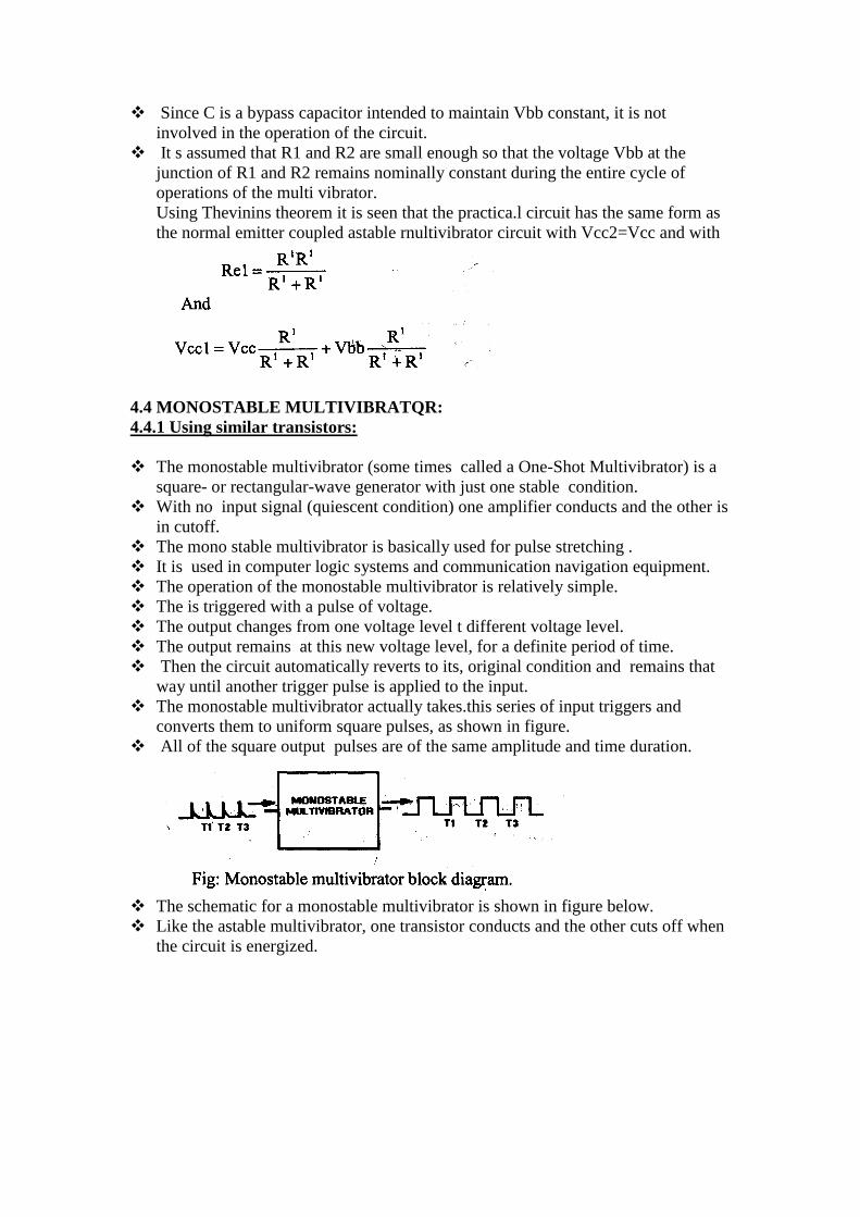
Using Thevinins theorem it is seen that the practica.l circuit has the same form as
the normal emitter coupled astable rnultivibrator circuit with Vcc2=Vcc and with
4.4 MONOSTABLE MULTIVIBRATQR:
4.4.1 Using similar transistors:
The monostable multivibrator (some times called a One-Shot Multivibrator) is a
square- or rectangular-wave generator with just one stable condition.
With no input signal (quiescent condition) one amplifier conducts and the other is
in cutoff.
The mono stable multivibrator is basically used for pulse stretching .
It is used in computer logic systems and communication navigation equipment.
The operation of the monostable multivibrator is relatively simple.
The is triggered with a pulse of voltage.
The output changes from one voltage level t different voltage level.
The output remains at this new voltage level, for a definite period of time.
Then the circuit automatically reverts to its, original condition and remains that
way until another trigger pulse is applied to the input.
The monostable multivibrator actually takes.this series of input triggers and
converts them to uniform square pulses, as shown in figure.
All of the square output pulses are of the same amplitude and time duration.
The schematic for a monostable multivibrator is shown in figure below.
Like the astable multivibrator, one transistor conducts and the other cuts off when
the circuit is energized.
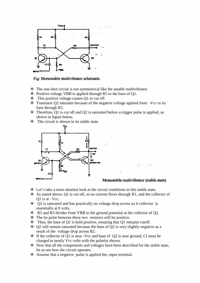
The one-shot circuit is not symmetrical like the astable multivibrator.
Positive voltage VBB is applied through R5 to the base of Q1.
This positive voltage causes Q1 to cut off.
Transistor Q2 saturates because of the negative voltage applied from –Vcc to its
base through R2.
Therefore, Q1 is cut off and Q2 is saturated before a trigger pulse is applied, as
shown in figure below.
The circuit is shown in its stable state.
Let‘s take a more detailed look at the circuit conditions in this stable state.
As stated above, Q1 is cut off, so no current flows through R1, and the collector of
Q1 is at –Vcc.
Q2 is saturated and has practically no voltage drop across so it collector is
essentially at 0 volts.
R5 and R3 divider from VBB to the ground potential at the collector of Q2.
The tie point between these two resistors will be positive.
Thus, the base of Q1 is held positive, ensuring that Q1 remains cutoff.
Q2 will remain saturated because the base of Q2 is very slightly negative as a
result of the voltage drop across R2.
If the collector of Q1 is near -Vcc and base of Q2 is near ground, Cl must be
charged to nearly Vcc volts with the polarity shown.
Now that all the components and voltages have been described for the stable state,
let us see how the circuit operates.
Assume that a negative pulse is applied the, input terminal.
C2 couples this voltage change to the base of Q1 and starts Q1 conducting.
Q1 quickly saturates, and its collector voltage immediately rises ground potential.
This sharp voltage increase is coupled through Cl to the base of Q2, causing Q2 to
cut off;
The collector voltage of Q2 immediately drops to V The voltage divider formed
by R5 and R3 then holds the base of Q1 negative, and Q1 is locked in saturation.
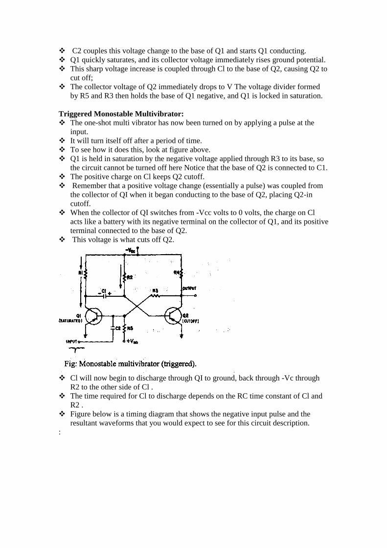
Triggered Monostable Multivibrator:
The one-shot multi vibrator has now been turned on by applying a pulse at the
input.
It will turn itself off after a period of time.
To see how it does this, look at figure above.
Q1 is held in saturation by the negative voltage applied through R3 to its base, so
the circuit cannot be turned off here Notice that the base of Q2 is connected to C1.
The positive charge on Cl keeps Q2 cutoff.
Remember that a positive voltage change (essentially a pulse) was coupled from
the collector of QI when it began conducting to the base of Q2, placing Q2-in
cutoff.
When the collector of QI switches from -Vcc volts to 0 volts, the charge on Cl
acts like a battery with its negative terminal on the collector of Q1, and its positive
terminal connected to the base of Q2.
This voltage is what cuts off Q2.
Cl will now begin to discharge through QI to ground, back through -Vc through
R2 to the other side of Cl .
The time required for Cl to discharge depends on the RC time constant of Cl and
R2 .
Figure below is a timing diagram that shows the negative input pulse and the
resultant waveforms that you would expect to see for this circuit description.
:
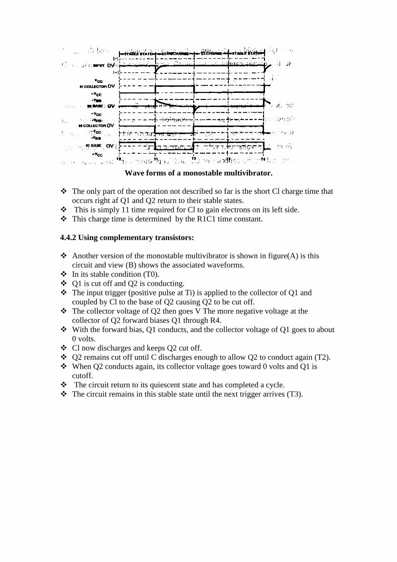
Wave forms of a monostable multivibrator.
The only part of the operation not described so far is the short Cl charge time that
occurs right af Q1 and Q2 return to their stable states.
This is simply 11 time required for Cl to gain electrons on its left side.
This charge time is determined by the R1C1 time constant.
4.4.2 Using complementary transistors:
Another version of the monostable multivibrator is shown in figure(A) is this
circuit and view (B) shows the associated waveforms.
In its stable condition (T0).
Q1 is cut off and Q2 is conducting.
The input trigger (positive pulse at Ti) is applied to the collector of Q1 and
coupled by Cl to the base of Q2 causing Q2 to be cut off.
The collector voltage of Q2 then goes V The more negative voltage at the
collector of Q2 forward biases Q1 through R4.
With the forward bias, Q1 conducts, and the collector voltage of Q1 goes to about
0 volts.
Cl now discharges and keeps Q2 cut off.
Q2 remains cut off until C discharges enough to allow Q2 to conduct again (T2).
When Q2 conducts again, its collector voltage goes toward 0 volts and Q1 is
cutoff.
The circuit return to its quiescent state and has completed a cycle.
The circuit remains in this stable state until the next trigger arrives (T3).
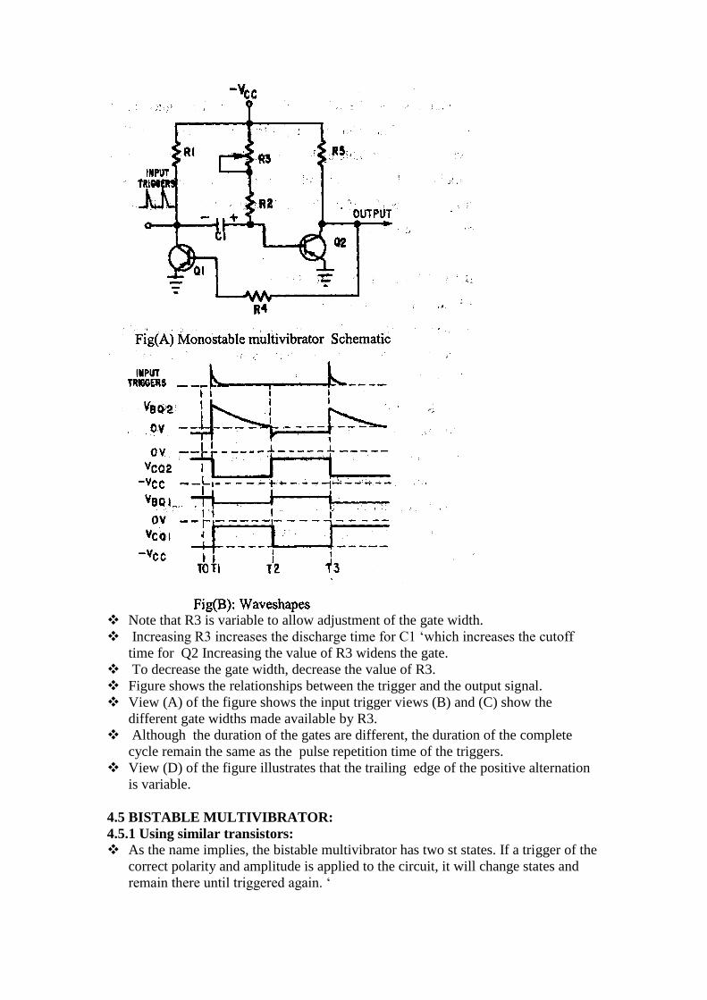
Note that R3 is variable to allow adjustment of the gate width.
Increasing R3 increases the discharge time for C1 ‗which increases the cutoff
time for Q2 Increasing the value of R3 widens the gate.
To decrease the gate width, decrease the value of R3.
Figure shows the relationships between the trigger and the output signal.
View (A) of the figure shows the input trigger views (B) and (C) show the
different gate widths made available by R3.
Although the duration of the gates are different, the duration of the complete
cycle remain the same as the pulse repetition time of the triggers.
View (D) of the figure illustrates that the trailing edge of the positive alternation
is variable.
4.5 BISTABLE MULTIVIBRATOR:
4.5.1 Using similar transistors:
As the name implies, the bistable multivibrator has two st states. If a trigger of the
correct polarity and amplitude is applied to the circuit, it will change states and
remain there until triggered again. ‗
The trigger need not have a fixed prf in fact, triggers from different sources,
occurring at different times can be used to switch this circuit.
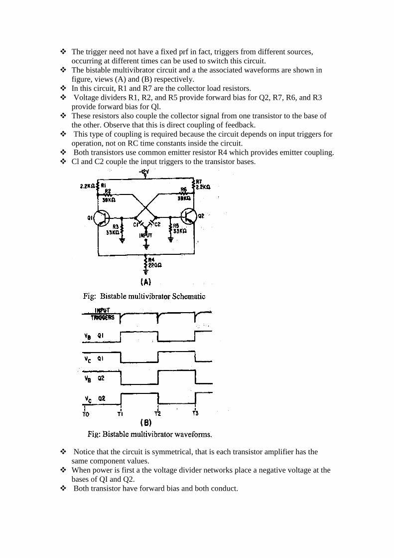
The bistable multivibrator circuit and a the associated waveforms are shown in
figure, views (A) and (B) respectively.
In this circuit, R1 and R7 are the collector load resistors.
Voltage dividers R1, R2, and R5 provide forward bias for Q2, R7, R6, and R3
provide forward bias for Ql.
These resistors also couple the collector signal from one transistor to the base of
the other. Observe that this is direct coupling of feedback.
This type of coupling is required because the circuit depends on input triggers for
operation, not on RC time constants inside the circuit.
Both transistors use common emitter resistor R4 which provides emitter coupling.
Cl and C2 couple the input triggers to the transistor bases.
Notice that the circuit is symmetrical, that is each transistor amplifier has the
same component values.
When power is first a the voltage divider networks place a negative voltage at the
bases of QI and Q2.
Both transistor have forward bias and both conduct.
Due to some slight difference between the two circuits, one transistor will
conduct more than the other.
Assume that Q1 conducts more than Q2.
The increased conduction of Q1 causes the collector voltage to be less negative
(more voltage drop across R1).
This decreases the forward bias of Q2 and decreases the conduction of Q2. When
Q2 conducts less, its collector voltage becomes more negative.
The negative-going change at the collector of Q2 is coupled to the base of Q1 and
causes Q1 to conduct even more heavily.
This regenerative action continues until Q2 is cut off and Q1 is saturated.
The circuit is in a stable state and will remain there until a trigger is applied to
change the state.
At T1, a negative trigger is applied to both bases through Cl and C2.
The trigger does not affect Q1 since it is already conducting.
The trigger overcomes cutoff bias on Q2 and causes it to conduct. As Q2 goes
into conduction, its collector voltage becomes positive.
The positive-going change at the Q2 collector causes a reverse bias on the base of
Q1.
As the conduction of Q1 decreases to the cutoff point, the collector voltage
becomes negative.
This switching action causes a rapid change of state with Q2 no conducting and
Q1 cut off.
At T2, a negative trigger is again applied to both bases.
This time, Q1 is brought into conduction and the regenerative switching action
cuts of Q2.
The bistable multivibrator will continue to change states is long as triggers are
applied
Notice that two input tnggers are required to produce one gate, one to turn it on
and the other to turn it off .
The input trigger frequency is twice the output frequency.
4.5.2 USING COMPLEMENTARY TRANSISTORS
The bistable multivibrator that most technicians know is commonly known by
other names: the ECCLES-JORDAN circuit and, more commonly, the FLIP-
FLOP circuit The flip-flop is a bistable multivibrator, ―bi‖ meaning two, that is,
the flip-flop has two stable states.
The flip-flop (f/f) can rapidly flip from one state to the other and then flop back to
its original state.
If a voltmeter were connected to the output of a flip-flop, it would measure either
a small positive or negative voltage, or a particularly low age (essentially 0 volts).
No matter which voltage is measured, the flip-flop would be stable.
Remember , stable means that the flip-flop will remain in a particular state
indefinitely.
It will not change states unless the proper type of trigger pulse is applied.

Flip-flops are used in switching-circuit applications(computer logic operations) as
counters, shift registers, clock pulse generators, and circuits.
They are also used for relay-control functions and for a variety applications in
radar and communications systems.
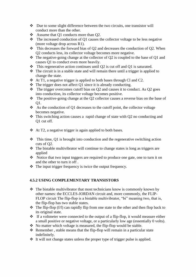
Notice that the basic flip-flop, illustrated in figure, has two inputs and two outputs.
The inputs are coupled to the bases of the transistors and the coupled from the
collectors of the transistors.
Think of the flip-flop as two emitter amplifier circuits, where the output of one
amplifier is connect of the other amplifier, and vice-versa.
Point (D) is connected through R4 to C4 to point (A).
Point (A) is the input to transistor Q1.
By the same token which is the output of Q1, is connected through R3 and C3 to
the input (point B ) of transistor Q2.
Taking a close look at the flip-flop circuit, you should be able to see how it
maintains its stable condition.
Typically for the resistors and applied voltages are shown in figure .
The capacitors have been removed for simplicity.
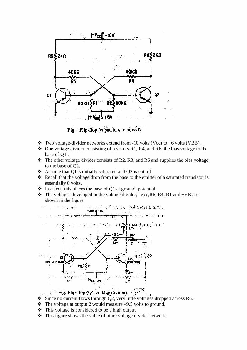
Two voltage-divider networks extend from -10 volts (Vcc) to +6 volts (VBB).
One voltage divider consisting of resistors R1, R4, and R6 the bias voltage to the
base of Q1 .
The other voltage divider consists of R2, R3, and R5 and supplies the bias voltage
to the base of Q2.
Assume that QI is initially saturated and Q2 is cut off.
Recall that the voltage drop from the base to the emitter of a saturated transistor is
essentially 0 volts.
In effect, this places the base of Q1 at ground potential .
The voltages developed in the voltage divider, -Vcc,R6, R4, R1 and ±VB are
shown in the figure.
Since no current flows through Q2, very little voltages dropped across R6.
The voltage at output 2 would measure –9.5 volts to ground.
This voltage is considered to be a high output.
This figure shows the value of other voltage divider network.
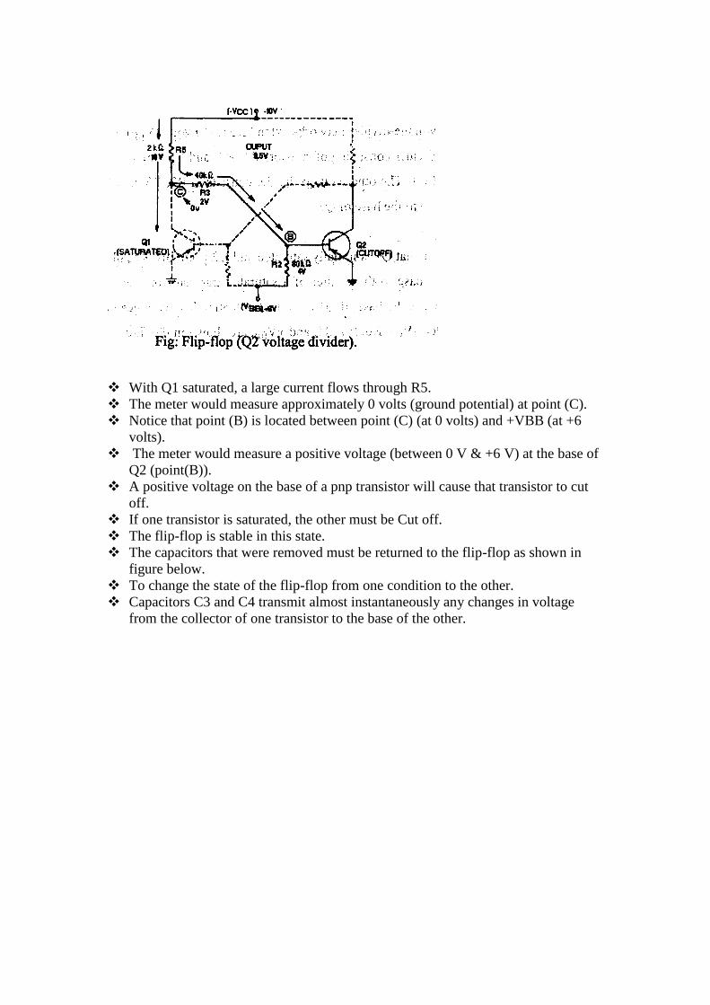
With Q1 saturated, a large current flows through R5.
The meter would measure approximately 0 volts (ground potential) at point (C).
Notice that point (B) is located between point (C) (at 0 volts) and +VBB (at +6
volts).
The meter would measure a positive voltage (between 0 V & +6 V) at the base of
Q2 (point(B)).
A positive voltage on the base of a pnp transistor will cause that transistor to cut
off.
If one transistor is saturated, the other must be Cut off.
The flip-flop is stable in this state.
The capacitors that were removed must be returned to the flip-flop as shown in
figure below.
To change the state of the flip-flop from one condition to the other.
Capacitors C3 and C4 transmit almost instantaneously any changes in voltage
from the collector of one transistor to the base of the other.
Capacitors C1 and C2 are input coupling
capacitors.
Leading edge of the positive pulse, this capacitor charges through a low input
resistance of the amplifier in series with the output impedance Rs of the trigger
source.
During the leading edge, the voltage across the capacitor large as the pulse
amplitude itself provided that Rs is small enough.
Then on application of negative going trailing edge of .the trigger pulse, the
input of transistor is driven negative by the amount equal to change across C.
But the binary is very sensitive to. any negative step at the input of the npn
transistor.
Hence a transition may occur at the trailing edge.
Usually it is desirable to triggering at the trailing edge.
This may be achieved by including a large resistance in series with C assuming
Rs is small.
TRIGGERING AT THE OUTPUT:
Triggering voltage may be applied at the output of one of the 2 stages of the
binary instead of being applied at the input.
Here again it is preferred to apply the trigger signal through a series capacitor
and a high value resistance as shown in figure.
This trigger signal immediately appears at the input of the other device, on
being transferred through the commutating capacitor.
Series resistor Rs serves to enhance the sensitivity of the transistor to a
negative pulse relative to that of the positive pulse.
This increased relative sensitivity results from the fact that the positive pulse
is required to be introduced at a point where the trigger signal looks through a
coupling capacitor at the collector of a conducting transistor offering low
impedance.
4.6.2 Symmetrical Triggering:
In a symmetrical trigger the trigger pulses are applied at only one input and
these are steered or directed to appropriate transistors sequentially.
Thus at each trigger pulse there results a change of the stable state.
Symmetrical collector triggering:
The figure gives the circuit of the binary using symmetric collector triggering
with negative triggering logic wherein the trigger tries to turn off a saturated
or on transistor.
Here Ct is the coupling capacitor.
The Rx - Ct network forms the differentiating network.
The input pulses after differentiation appear at a point P to which the cathodes
of 2 steering diodes D1and D2 are connected.
Anodes of the diodes Dl and D2 are connected to the collector of the
transistor T1 and T2 respectively.
With transistor T21 off there is no collector current and hence 0 voltage drop
across resistor Rc1.
The collector voltage of TI equals the supply voltage Vcc.
The anode and the cathode of the diode Dl are at the same potential namely
Vcc.
Thus diode Dl is forward biased.
The voltage drop across the collector circuit resistor RC2 of the conduting
transistor T2 makes the collector voltage of T2 very low equal to Vc2.
Thus anode of the diode D2 is at low potential while the cathode is at the
supply potential Vcc.
Hence D2 is reverse biased.
The differential pulse appears at point P.
Polarity of steering diodes is such that they block the transmission of positive
pulses.
Negative trigger pulses follow the low impedance path offered by the diode
D1 and coupling network R3- Cm2 to the base of transistsor T2.
Now tile diode D1 is reverse biased while diode D2 is forward biased.
Next, negative trigger gets transmitted through D2 and appears at the
collector of the off transistor T2.
This negative pulse trigger passes through the coupling network Rl — Cml,
appears at the base of the on transistor T1 and turns it off.
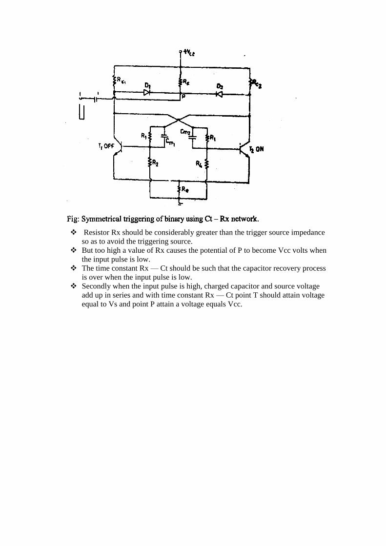
Resistor Rx should be considerably greater than the trigger source impedance
so as to avoid the triggering source.
But too high a value of Rx causes the potential of P to become Vcc volts when
the input pulse is low.
The time constant Rx — Ct should be such that the capacitor recovery process
is over when the input pulse is low.
Secondly when the input pulse is high, charged capacitor and source voltage
add up in series and with time constant Rx — Ct point T should attain voltage
equal to Vs and point P attain a voltage equals Vcc.
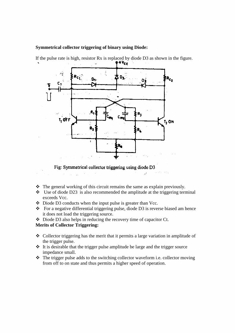
Symmetrical collector triggering of binary using Diode:
If the pulse rate is high, resistor Rx is replaced by diode D3 as shown in the figure.
The general working of this circuit remains the same as explain previously.
Use of diode D23 is also recommended the amplitude at the triggering terminal
exceeds Vcc.
Diode D3 conducts when the input pulse is greater than Vcc.
For a negative differential triggering pulse, diode D3 is reverse biased am hence
it does not load the triggering source.
Diode D3 also helps in reducing the recovery time of capacitor Ct.
Merits of Collector Triggering:
Collector triggering has the merit that it permits a large variation in amplitude of
the trigger pulse.
It is desirable that the trigger pulse amplitude be large and the trigger source
impedance small.
The trigger pulse adds to the switching collector waveform i.e. collector moving
from off to on state and thus permits a higher speed of operation.
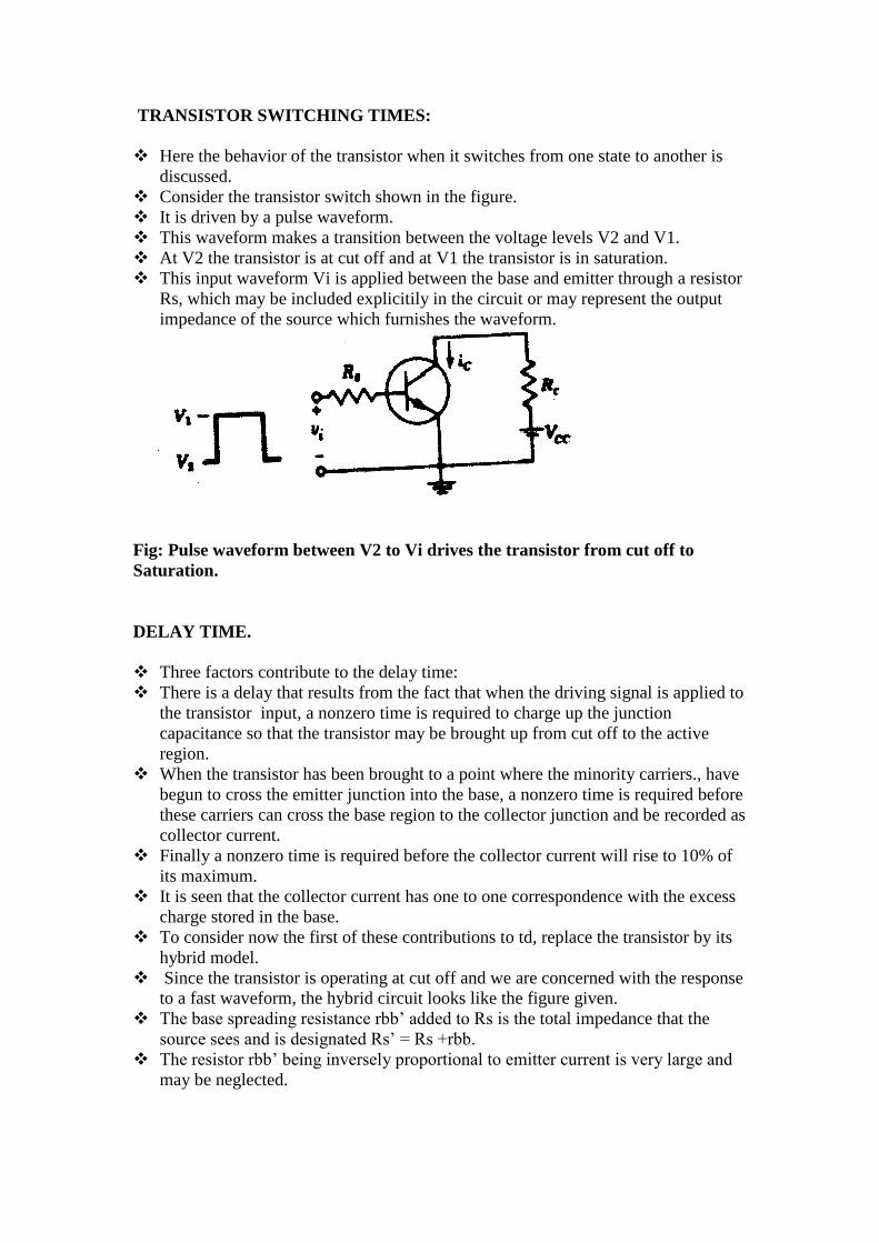
TRANSISTOR SWITCHING TIMES:
Here the behavior of the transistor when it switches from one state to another is
discussed.
Consider the transistor switch shown in the figure.
It is driven by a pulse waveform.
This waveform makes a transition between the voltage levels V2 and V1.
At V2 the transistor is at cut off and at V1 the transistor is in saturation.
This input waveform Vi is applied between the base and emitter through a resistor
Rs, which may be included explicitily in the circuit or may represent the output
impedance of the source which furnishes the waveform.
Fig: Pulse waveform between V2 to Vi drives the transistor from cut off to
Saturation.
DELAY TIME.
Three factors contribute to the delay time:
There is a delay that results from the fact that when the driving signal is applied to
the transistor input, a nonzero time is required to charge up the junction
capacitance so that the transistor may be brought up from cut off to the active
region.
When the transistor has been brought to a point where the minority carriers., have
begun to cross the emitter junction into the base, a nonzero time is required before
these carriers can cross the base region to the collector junction and be recorded as
collector current.
Finally a nonzero time is required before the collector current will rise to 10% of
its maximum.
It is seen that the collector current has one to one correspondence with the excess
charge stored in the base.
To consider now the first of these contributions to td, replace the transistor by its
hybrid model.
Since the transistor is operating at cut off and we are concerned with the response
to a fast waveform, the hybrid circuit looks like the figure given.
The base spreading resistance rbb‘ added to Rs is the total impedance that the
source sees and is designated Rs‘ = Rs +rbb.
The resistor rbb‘ being inversely proportional to emitter current is very large and
may be neglected.
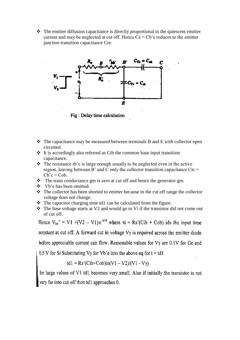
The emitter diffusion capacitance is directly proportional to the quiescent emitter
current and may be neglected at cut off. Hence Ce = Cb‘e reduces to the emitter
junction transition capacitance Cre
The capacitance may be measured between terminals B and E with collector open
circuited.
It is accordingly also referred as Cib the common base input transition
capacitance.
The resistance rb‘c is large enough usually to be neglected even in the active
region, leaving between B‘ and C only the collector transition capacitance Ctc =
Cb‘c = Cob.
The trans conductance gm is zero at cut off and hence the generator gm.
Vb‘e has been omitted.
The collector has been shorted to emitter because in the cut off range the collector
voltage does not change.
The capacitor charging time td1 can be calculated from the figure.
The base voltage starts at V2 and would go to Vi if the transistor did not come out
of cut off.
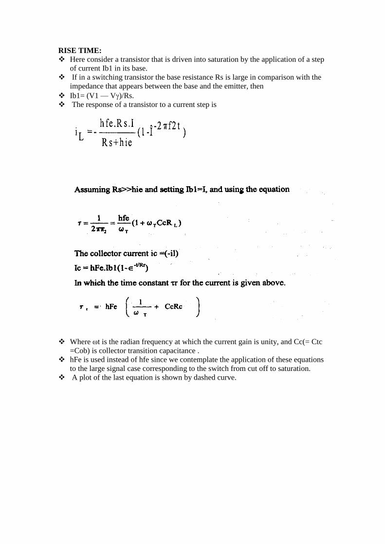
RISE TIME:
Here consider a transistor that is driven into saturation by the application of a step
of current Ib1 in its base.
If in a switching transistor the base resistance Rs is large in comparison with the
impedance that appears between the base and the emitter, then
Ib1= (V1 — V)/Rs.
The response of a transistor to a current step is
Where ωt is the radian frequency at which the current gain is unity, and Cc(= Ctc
=Cob) is collector transition capacitance .
hFe is used instead of hfe since we contemplate the application of these equations
to the large signal case corresponding to the switch from cut off to saturation.
A plot of the last equation is shown by dashed curve.
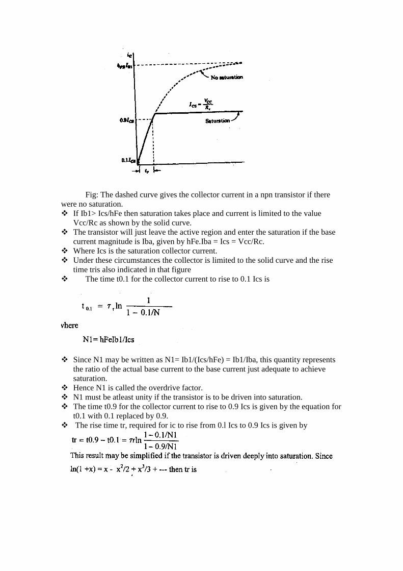
Fig: The dashed curve gives the collector current in a npn transistor if there
were no saturation.
If Ib1> Ics/hFe then saturation takes place and current is limited to the value
Vcc/Rc as shown by the solid curve.
The transistor will just leave the active region and enter the saturation if the base
current magnitude is Iba, given by hFe.Iba = Ics = Vcc/Rc.
Where Ics is the saturation collector current.
Under these circumstances the collector is limited to the solid curve and the rise
time tris also indicated in that figure
The time t0.1 for the collector current to rise to 0.1 Ics is
Since N1 may be written as N1= Ib1/(Ics/hFe) = Ib1/Iba, this quantity represents
the ratio of the actual base current to the base current just adequate to achieve
saturation.
Hence N1 is called the overdrive factor.
N1 must be atleast unity if the transistor is to be driven into saturation.
The time t0.9 for the collector current to rise to 0.9 Ics is given by the equation for
t0.1 with 0.1 replaced by 0.9.
The rise time tr, required for ic to rise from 0.l Ics to 0.9 Ics is given by
For this condition of heavy overdrive the rise time is independent of hFe because
r / hFe does not depend upon hFe.
For this reason and because tr varies inversely with lb 1 it is advantageous to drive
the transistor well into saturation with a large base current if it is desired to
minimize the turn on time.
STORAGE TIME:
The transistor fails to respond to the trailing edge of the driving pulse for t time
interval ts.
This is due to the fact that a transistor in saturation has a charge of excess
minority carriers stored in the base.
The transistor cannot respond until this saturation excess charge has been
removed.
In the active region the excess minority carriers which are injected into the base at
the emitter junction diffuse across the base and on reaching the second junction
constitute the collector current.
Storage time calculation:
The storage time ts can be calculated now:
This time is broken into 2 parts the first of which is tsl is the time from the
occurrence of the end of the pulse to the time when the collector current just
begins to change.
The second part ts2 is the time requires for ic to fall to 90% of Ics.
Tsl can be found as follows.
Icn(s)=-αn(s)Ien(s) Ie1(s)=- α(s)Ic1(s)
Ie(s)=Ien(s)+Ie1(s) Ic(s)+Ic1(s).
SCHMITT TRIGGER CIRCUIT:
Schmitt trigger is a voltage comparator that develops a regenerative trigger
action.
A basic circuit of schmitt trigger is shown in the figure.
It is drawn using differentiator followed by an inverter.
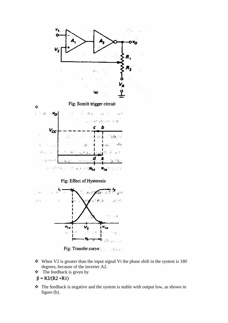
When V2 is greater than the input signal Vi the phase shift in the system is 180
degrees, because of the inverter A2.
The feedback is given by
The feedback is negative and the system is stable with output low, as shown in
figure (b).
The amplifier gains are large as soon as the signal Vi exceeds V2 the phase shift
of Al goes to 180 degrees giving a total of 360 degrees phase shift .
This ensures the establishment of a positive feedback condition.
This makes the switching action very rapid and places Vo at Vcc of the amplifier
with the input at V1a.
The circuit remains in this switched state as long as V1 > V2.
When V1 falls the amplifier output remains stable until V1 reaches the value V1c
when the phase angle of the overall gain reverts to its original 180 degrees
condition, with negative feedback and the circuit switches back to its original
condition.
Figure ( c ) illustrates the cause of the output hysteresis, showing it duel the very
small signal changes Vb needed to drive the amplifier to saturation or cut off
conditions.
The threshold voltage V2 is established by adjustment of the control on R1
R2.
The steady component of V2 can be written from the voltage divider action as
Steady state V2 = Vr.R1/(R1 +R2).
The feedback component is dependent on the output as Signal
V2 = ± Al A2.Vi.R2/(Ri +R2)
The switching levels are therefore given by
The following figure shows discrete component forms of the schmitt trigger
circuit.
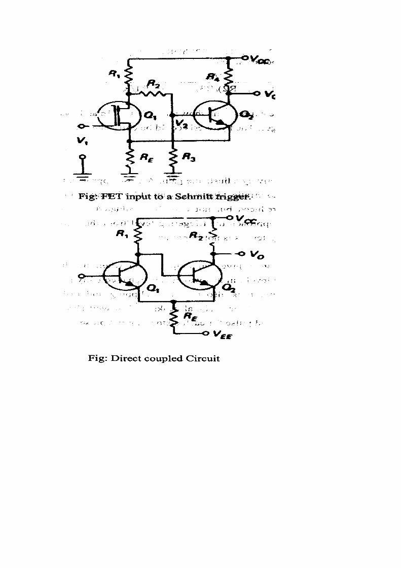
In fig (a) a MOSFET is used to eliminate erratic effects introduced by input
resistance variation with a junction transistor.
The figure in (a 0 can be correlated with the previous basic diagram.
Transistor Q1 serves as the differential amplifier, with its inverting input at the
base and the feedback input at the emitter.
Transistor Q2 provides the inverting gain A2.
The circuit can also be viewed as a multivibrator with one of the cross coupling
networks replaced by emitter coupling.