4.5: 200 dpi 4-a-si:h tfts current-driven am-pleds sid 2003.pdf4.5 / y. hong 22 • sid 03 digest...
TRANSCRIPT

4.5 / Y. Hong
22 • SID 03 DIGEST
4.5: 200 dpi 4-a-Si:H TFTs Current-Driven AM-PLEDs
Yongtaek Hong, Jeong-Yup Nahm* and Jerzy Kanicki Solid-State Electronics Lab., Dept. of EECS, The University of Michigan, Ann Arbor, MI, USA
* Currently at Cypress Semiconductor Corp., San Jose, CA, USA
Abstract In this paper, for the first time, we report 200 dpi current-driven active-matrix organic polymer light-emitting displays based on five-terminal, four amorphous silicon thin-film transistors (TFTs) pixel electrode circuits, which compensate for the threshold voltage shift of organic polymer light-emitting devices and TFTs.
1. Introduction Since hydrogenated amorphous silicon (a-Si:H) thin-film transistors (TFTs) active-matrix arrays can be fabricated at low cost and with a high uniformity over large areas, it is expected that this mature technology will become preferred in comparison with the poly-crystalline silicon (poly-Si) technology [1-3] for the active-matrix organic light-emitting display (AM-OLED). Furthermore, the recent enhancement of organic light-emitting devices (OLEDs) performances [4] has made it easier to extend a-Si:H TFTs-based technology to AM-OLED. In AM-OLED, a-Si:H TFTs act as switching and driving devices to the OLEDs in a pixel electrode circuit. To drive light-emitting devices, a continuous excitation during the whole frame period is needed for high-performance AM-OLEDs. This can be very demanding task for a-Si:H TFTs. But a previously proposed current-source four-a-Si:H TFTs pixel electrode circuit [5] is capable of providing sufficient current for the OLEDs. Circuit simulation and experimental results [6] showed that this pixel electrode circuit with four a-Si:H TFTs can fully compensate for TFT threshold voltage shift, consequently providing a constant current flow through OLEDs. In this paper, for the first time, we report on opto-electronic properties of 4-a-Si:H TFTs current-driven AM-organic polymer light-emitting display (AM-PLED). We have clearly demonstrated that this type of pixel electrode circuit can provide continuous constant current flow over organic polymer light-emitting devices (PLEDs) during the whole frame period. And based on the experimental results, we concluded that this pixel electrode circuit is suitable for high performance AM-PLED.
2. 4-a-Si:H TFTs pixel electrode circuit Figure 1 shows the schematic diagram of 4-a-Si:H TFTs pixel electrode circuit. T1/T2, T3, and T4 are selecting, driving, and switching TFTs, respectively. The T1/T2 and T4, control the current flow path according to appropriate selecting voltage signals (Vselect1 and Vselect2). During the select time (Vselect1 is high, Vselect2 is low), T1/T2 are ON and T3 is OFF, directing the data current flow from data line (Idata) to PLED through T1/T2 and T3, which is indicated as a solid line in Fig. 1. After the storage capacitor (CST) is charged up during the select time, Vselect1 and Vselect2 signals change during the rest of the frame time (Vselect1 is low, Vselect2 is high), turning T1/T2 OFF and T4 ON, respectively. Then, the same amount of data current will flow from VDD to ground through T4, T3, and PLED, which is indicated as a dotted
line in Fig. 1. During the select time, gate-source (VGS_T3) and drain-source (VDS_T3) voltage values of T3 are set to certain values to achieve IPLED = Idata with the help of charges stored in CST. These VGS_T3 and VDS_T3 can vary from pixel-to-pixel to maintain Idata = IPLED independent of the PLEDs and TFTs operating parameters. Examples of the device parameter variations are PLEDs and TFTs threshold voltages, and TFTs mobility, which could result from manufacturing and material variations, and pixel electrode circuit aging. During the rest of the frame time, IPLED should be maintained very close to the current flow through the PLED (Idata) during the select time. Since circuit configuration and driving conditions are designed for the driving TFT (T3) to operate in the saturation regime during the whole frame time, the current flow to PLED through T3 does not change significantly for the same VGS_T3 although the VDS_T3 value changes due to the current flow path change during the rest of the frame time. However, if a-Si:H TFTs shows non-ideal characteristics in the saturation regime, IPLED could be affected by VDS_T3 change during the frame time, leading to the IPLED unequal to the Idata. IPLED can also be affected by the change of the stored voltage in CST due to the charge redistribution of CST by TFT parasitic capacitances of T1, and/or any leakage current through T1/T2 during the frame time.
3. 4-a-Si:H TFTs active-matrix arrays We used Corning 1737 glass substrates to fabricate 4-a-Si:H TFTs active-matrix arrays. Chromium (Cr, 2000 Å) layer was deposited on the glass substrates by the DC sputtering method and, then Cr gates and selection lines were patterned by wet-etching (Mask #1). Following gate line definition, a-SiNx:H (3000 Å)/a-Si:H
Idata Vselect1
Vselect2
CST
PLED
IPLED
T1
T2
T3
T4
VDD
VDS_T2+ -
VDS_T1+ -
+-
VDS_T3
+-
VPLED
+
-VDS_T4
Figure 1. Schematic diagram of 4-a-Si:H TFTs pixel electrode circuit.
ISSN/0003-0966X/03/3401-0022-$1.00+.00 © 2003 SID
4.5 / Y. Hong
SID 03 DIGEST • 23
(1000 Å)/n+ a-Si:H (300 Å) tri-layer was deposited by plasma enhanced chemical vapor deposition (PECVD) method. Using the reactive ion etching (RIE) with a gas mixture of O2 and CCl2F2, we defined the device active islands (Mask #2). Then, the gate via was patterned through the a-SiNx:H layer by wet-etching in buffered hydrofluoric acid (BHF) (Mask #3). Molybdenum (Mo, 2000 Å) was used for the source/drain electrodes and Idata/VDD lines. Mo layer was deposited by the DC sputtering method and then, patterned by wet-etching (Mask #4). After that, we performed back-channel-etching by RIE with a gas mixture of O2 and CCl2F2. To improve the source/drain contact properties, the fabricated active-matrix arrays were annealed for two hours at 230 °C under the nitrogen environment. To evaluate our active-matrix arrays processes before the next fabrication steps are performed, we measured the electrical characteristics of TFTs, which will be discussed in Section 5. Then, we spun-coated benzocyclobutene (BCB, 1~1.5 㯀m) on top of the fabricated active-matrix arrays to provide a planarized, flat surface for the following indium tin oxide (ITO) and PLED layers. After the BCB layer was coated, the active-matrix arrays were cured at
carefully controlled temperature steps under a good nitrogen environment. To make a contact for the following ITO layer, via was formed through the cured BCB planarization layer by using RIE with a gas mixture of O2 and CF4 (Mask #5). After via definition, the in-situ argon (Ar) back-sputtering was performed on the BCB layer surface before ITO deposition, which improves the adhesion between ITO and BCB layer. ITO (1000 Å) was deposited by DC sputtering method and then, patterned by wet-etching in a mixture solution of nitric acid (HNO3), hydrochloric acid (HCl), and deionized water (Mask #6). The size (W/L) of each TFT is 15/6, 55/6, 58/6, and 70/6 for T1, T2, T3, and T4, respectively. The top view of the fabricated 200 dpi AM-PLED (0.5 inch × 0.5 inch, 100 × 100 pixels) is shown in Fig. 2. The top view and cross-section of each pixel are also included. The aperture ratio (AR) of each pixel is about 10%, which is defined as the ratio of the PLED area (24×65 㯀m2) to the whole pixel area (127×127 㯀m2).
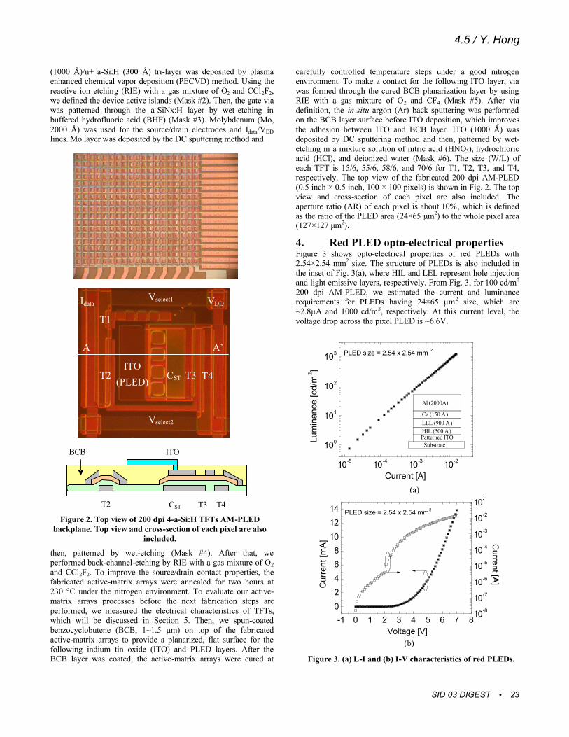
4. Red PLED opto-electrical properties Figure 3 shows opto-electrical properties of red PLEDs with 2.54×2.54 mm2 size. The structure of PLEDs is also included in the inset of Fig. 3(a), where HIL and LEL represent hole injection and light emissive layers, respectively. From Fig. 3, for 100 cd/m2 200 dpi AM-PLED, we estimated the current and luminance requirements for PLEDs having 24×65 µm2 size, which are ~2.8µA and 1000 cd/m2, respectively. At this current level, the voltage drop across the pixel PLED is ~6.6V.
(b)
Figure 3. (a) L-I and (b) I-V characteristics of red PLEDs.
10-5 10-4 10-3 10-2
100
101
102
103
Lum
inan
ce [c
d/m
2 ]
Current [A]
PLED size = 2.54 x 2.54 mm 2
Al (2000A)
LEL (900 A)HIL (500 A)Patterned ITOSubstrate
Ca (150 A)
-1 0 1 2 3 4 5 6 7 802468
101214
10-8
10-7
10-6
10-5
10-4
10-3
10-2
10-1
Cur
rent
[mA]
Voltage [V]
Current [A]
PLED size = 2.54 x 2.54 mm2
(a)
ITO BCB
T2 CST T3 T4
Figure 2. Top view of 200 dpi 4-a-Si:H TFTs AM-PLED backplane. Top view and cross-section of each pixel are also
included.
T4
T1
T2 ITO
(PLED) CST T3
VDD Idata Vselect1
Vselect2
A A’

4.5 / Y. Hong
24 • SID 03 DIGEST
5. Electrical properties of 4-a-Si:H TFTs Figure 4 shows the electrical characteristics of each TFT in the 4-a-Si:H TFTs pixel electrode circuit. For selecting and switching transistor T1/T2 and T4, the measured transfer characteristics (VDS = 0.1 V) are shown in Fig. 4(a). We extracted the field-effect mobility and threshold voltage of TFTs from those characteristics, which are 0.7 cm2/Vs and 8.6 V, respectively. Since T3 operates in saturation regime, IDS-VDS characteristics of T3 were measured for different VGS values as shown in Fig. 4(b). From this figure, we can conclude that the driving TFT (T3) of our 4-a-Si:H TFT pixel electrode circuit is capable of providing up to 10 㯀A for rather low VGS_T3 and VDS_T3 values (less than 20 V). We have used PLED and a-Si:H TFTs characteristics to select the driving conditions of our pixel electrode circuit.
6. 4-a-Si:H TFTs 200 dpi AM-PLED Before we deposited PLED active layers, the fabricated active-matrix arrays was thoroughly cleaned in photo resist (PR) stripper, acetone, and isopropyl alcohol (IPA) to remove any residual PR on defined ITO pixel electrode. In addition, the ITO surface was exposed to UV-ozone treatment for 10 minutes. First, we spun-coated poly (3,4-ethylene dioxythiophene) (PEDOT) doped with poly (styrenesulfonate) (PSS) and cured for 20 minutes at 90 °C in the vacuum oven. Then, we spun-coated red light-emitting poly (fluorene) copolymer in xylene solution and cured for one hour at 90 °C in the vacuum oven. All the spin-coating processes were performed at room temperature in the air. Finally, a calcium (150 Å)/aluminum (2000 Å) bi-layer cathode was thermally evaporated through a shadow mask without breaking vacuum under ~10-6 Torr. All the cathode electrodes for each pixel are connected in our AM-PLED. We removed the PLED active layers coated on the display contact pads by using solvent. For display evaluation, we operated our AM-PLED by applying constant 30 V, 0 V, and 30 V to Vselect1, Vselect2 and VDD lines, respectively. The 0~25 mA data currents were applied to Idata lines to measure the display luminance at different data current levels. The display driving conditions are indicated as bold italic values in Fig. 5. The required signal waveforms for the real display operation are also included in this figure. Figure 6 shows the demonstration of red light-emitting 200 dpi AM-PLED when the data current is 25 mA. The AM-PLED shows the pixel light-emission yields of about 75%. The magnified image of each pixel light-emission is also included in Fig. 6. The opto-electrical characteristics of the display has been measured using an integrating sphere and a calibrated photo-detector connected to a radiometer to measure the total luminous flux from the display [7]. All the measurements have been performed in the air at room temperature. Fig. 7 shows the luminous flux versus applied data current characteristics. The initial light emission was observed when the data current is about 1-2 mA. We obtained up to 1.1 × 10 -2 lumen when the data current is 25 mA. For the Lambertian emitter, we can calculate luminance (L) from the measured luminous flux (㩠) by using the following equation;
Figure 5. Driving schemes for 200 dpi AM-PLED. * bold italic values show the driving conditions used in this work.
(b)
Figure 4. (a) IDS-VGS characteristics at VDS = 0.1 for selecting and switching TFTs (T1/T2 and T4) and (b) IDS-
VDS characteristics for driving TFT (T3).
-10 0 10 20 300.0
0.1
0.2
0.3
0.4
10-14
10-13
10-12
10-11
10-10
10-9
10-8
10-7
10-6
T1 T2 T4
I DS_
T1,2
,4 [µ
A]
VGS_T1,2,4 [V]
IDS_T1,2,4 [A]
0 5 10 15 20 25
0
5
10
15
20
25
10 V
15 V
20 V
25 V
I DS_
T3 [µ
A]
VDS_T3 [V]
VGS_T3
(a)

4.5 / Y. Hong
SID 03 DIGEST • 25
AL
×Φ
=π
(1)
,where A is the are of the light emitter. By assuming that our AM-PLED is a Lambertian emitter, we can calculate the display luminance (LDisplay) by considering the display area and pixel light-emission yield (A = 1.27cm × 1.27cm * 0.75 = 1.215×10⁻⁴ m2), which is plotted for different data current levels in Fig. 7. We obtained about 30 cd/m2 at the data current level of 25 mA. In addition, if we consider both the pixel PLEDs area of the display and the pixel light emission yield, we can calculate the effective emission luminance (LEmission). In this case, A = (pixel PLED area in each pixel) × (total number of pixel) × (pixel light-emission yield) = 25 × 65 㯀m2 × 100 × 100 × 0.75 = 1.125×10⁻⁵ m2. The obtained LEmission versus applied data current is shown in Fig. 7. Up to 300 cd/m2 has been obtained at the data current level of 25 mA
7. Conclusions In this paper, for the first time, we demonstrated red 200 dpi current-driving 4-a-Si:H TFTs AM-PLED with 0.5 inch2 size (100×100 pixels). The display and emission luminance were obtained up to 30 and 300 cd/m2 at the data current level of 25 mA, respectively.
8. Acknowledgements This work was supported by NIH grant. The authors would like to thank Dr. I. French at Philips Research Laboratory, U.K. for assistance with the PECVD. The authors also would like to thank Professor Reiji Hattori at Kyushu University, Japan, for discussion on pixel circuit design, and thank Dr. J-H Kim at University of Michigan for technical discussion on active-matrix array processing. The first light-emission of our display was observed on March 4, 2003.
9. References [1] Dawson, R.M.A., Shen, S., Furst, D.A., Connor, S., Hsu, J.,
Kane, M.G., Stewart, R.G., Ipri, A., King, C.N., Green, P.J., Flegal, R.T., Pearson, S., Barrow, W.A., Dickey, E., Ping, K., Robinson, S., Tang, C.W., Van Slyke, S., Chen, F., Shi, J., Lu, M.H., Moskewicz, M., and Sturm, J.C., Proc. of SID Sym., 438 (1999).
[2] Shimoda, T., Kimura, M., and Miyashita S., Proc. of IEDM, 107 (1999).
[3] Sasaoka, T., Sekiya, M., Yumoto, A., Yamada, J., Hirano, T., Iwase, Y., Yamada, T., Ishibashi, T., Mori, T., Asano, M., Tamura, S., and Urabe, T., Proc. of SID Sym., 384 (2001).
[4] Hack, M., Kwong, R., Weaver, M.S., Lu, M., and Brown, J.J., Proc. of IDMC, 57 (2002).
[5] He, Y,. Hattori, R., and Kanicki, J., IEEE Elec. Dev. Lett. 21, 590 (2000).
[6] Kanicki, J., Kim, J-H, Nahm, J-Y, He, Y., and Hattori, R., Proc. of Asia Display, 315 (2001).
[7] Hong, Y. and Kanicki, J., Proc. of Asia Display, 1443 (2001).
Even data lines
Odd data lines
Vselect1 lines
Vselect2 lines
GND
VDD
Figure 6. Top view of illuminated 200 dpi 4-a-Si:H TFTs AM-PLED. Magnified image of each pixel light-emission is
also included.
Figure 7. Luminous flux and calculated luminance of 200 dpi AM-PLED versus applied data current.
1 10
10-4
10-3
10-2
10-1
10-1
100
101
102
103
Lum
inou
s Fl
ux [l
m]
Applied Data Current [mA]
LDisplay
LEmission
Luminance [cd/m
2]