5.2 materials scienceiuac.res.in/reres/pub/ar/2010/chapter 5-2.pdf · mechanical stability of lahcl...
TRANSCRIPT

147
5.2 Materials science
There have been a large number of experiments in materials science with energetic ion beams on the problems mainly related to ion beam induced modifications and a few on characterization of materials.
The ERDA facility was used for hydrogen content measurement in Mg and Mg/Al films capped with Pd layer and the H loss measurements in MCT films under SHI irradiation. The evolution of gases like H2O, O2, CO, CO2, C2H2 etc. were monitored by on-line QMA in irradiation of LAHcl and LA2HBr single crystals. The study on evolved gases monitored by online QMA gave an insight to the possible reactions within the ion track core, occurring in the ion irradiation of Ni film deposited on PTFE system.
The irradiation chamber and in-situ XRD facility in beam hall II were also used in a few user experiments this year. Ion beam mixing experiments were performed on Te/Be, In/Te and Mn/Si systems. Experiments on defect annealing and damage of CNT’s by swift heavy ions were performed. Surface plasmon tuning of the Ag-C60 nanocomposite thin films was demonstrated by ion irradiation. Surface studies of the SHI irradiated ultra thin Au films were performed and is under further investigation to study sputtering and formation of nanostructures.
SHI irradiation induced modifications studies were performed on different nanocomposite systems such as Ni-Alumina, ZnO-PMMA, SnO2-PPY, Fe2O3-polymer etc. Si nanosprings were irradiated by SHI to study the influence of SHI irradiation on mechanical stiffness. Precipitation of Ge nanoparticles in Ge-silica composite under SHI radiation was investigated. Surface nanostructures were created on MgO and LaAlO3 films by SHI irradiation. SHI irradiation studies on ZnFe particles and BaTiO4 particles were performed.
SHI irradiation induced modifications in GaN, SnN and Mn doped ZnO were studied. The enhancement in resistivity switching properties as a result of irradiation of Ag/LSMO planar structure was observed. The gas sensing sensitivity of HAP thin films were enhanced by SHI irradiation. SHI irradiation of various polymers such as PVDC, polyanalin, P3HT, Makrafol and PET were performed to study the ion beam induced modifications. Low energy ions from LEIBF were used to create the nanostructures at the surface of CdS thin film.
Several experiments were performed on different possible dosimetery materials for TL dosimeter applications. The electrical characterization studies of the pristine and irradiated device chips used in space vehicles were also carried out.

148
5.2.1 HydrogencontentinMgandMg/AlfilmsbyERDA
Pragya Jain1, Ankur Jain1, Devendra Vyas1, S. A. Khan2, D. Kabiraj2, I.P.Jain1
1Centre for Non-Conventional Energy Resources, University of Rajasthan, Jaipur 2Inter University Accelerator Center, Aruna Asif Ali Marg, New Delhi
Interaction of hydrogen with solid-state surfaces is a topic of research interest due to complex physical and chemical processes involved and also due to its direct relevance to technologically important applications of hydrogen storage, sensing, and switching [1,2]. In general, these applications require faster and increased H incorporation during loading followed by complete/maximum removal during deloading. In the present work investigations on the hydrogen concentration profile in as-deposited and H-loaded Pd capped Mg and Mg/Al films have been undertaken using high energy 120MeV Ag9+ ions.
Vapor deposition unit equipped with 3KW electron gun and two thermal evaporation units for sequential deposition has been used to prepare Pd/Mg/Pd and Pd/Mg/Al./Pd films on Si substrate at 10-7 torr vacuum. Hydrogenation of the films was carried out at 230oC under H2 pressure of 5bar in a SS chamber for 2hrs. The chamber was pumped down to 10-5 torr before introducing hydrogen to it. Areal concentration of hydrogen (NH in atoms/cm2) of both as-deposited and hydrogenated films was measured by ERDA using 120MeV Ag9+ beam. The hydrogen recoils were detected in a Si surface barrier detector (SSBD) kept at 30oC from recoil angle with polypropylene stopper foil in front of it to stop other recoils. The areal concentration of H was calculated from the integral counts (Y) of the recoil energy spectra, with the help of the equation:
N=Ysinα / [Np(dσ/dΩ)] --------------------(1)
The variation of H-concentration (atoms/cm2) against incident ion fluence (ions/cm2) of Ag9+ ions for as deposited and H-loaded Mg and Mg/Al films were recorded. It has been observed that H-content of the films decreases with increase in ion fluence.
The values of H in Pristine and H loaded samples estimated by ERDA are given in table 1.
Table1: H concentration values for as-deposited (XD) and hydrogen loaded (XL) samples
Sample XD(atoms/cm2) XL (atoms/cm2) Pd/Mg/Pd 2.2*1017 4.0*1017
Pd/Mg/Al./Pd 3.2*1017 8.6*1018
The phase identification and surface modifications due to hydrogenation will be studied using XRD and AFM.
The ERDA results reveal an increase in hydrogen concentration in metallic thin films on hydrogen loading. The addition of Al destabilizes the magnesium hydride as reported

149
by Guo et al [3, 4] which leads to hydrogen penetration to greater depths, causing a higher H-content in Pd/Mg/Al./Pd system.
reFerences
[1] T. Xu, M. P. Zach, Z. L. Xiao, D. Rosenmann, U. Welp, W. K. Kwok, and G. W. Crabtree, Appl Phys. Lett. 86 (2005) 203104.
[2] J. N. Huiberts, R. Griessen, J. H. Rector, R. J. Wijngaarden, J. P. Dekker, D. G. de Groot, and N. J. Koeman, Nature (London) 380 (1996) 231.
[3] Y. Song, Z.X. Guo, R. Yang, Phys. Rev. B 69 (2004) 094205.[4] C.X. Shang, M. Bouodina, Y. Song, Z.X. Guo, Int. J. Hydrogen Energy 29 (2004) 73–80.
5.2.2 In-situQuadrupolemassanalyzerofionirradiatedLAHCl.H2O and la2HBr.H2OsinglecrystalsandeffectofionirradiationonLAHCl.H2Osinglecrystal
K. Sangeetha1, R. Ramesh Babu1,*, Jai Prakash2, S. A. Khan2, K. Asokan2 and D. K. Avasthi2
1 Department of Physics, Bharathidasan University, Tiruchirappalli 2 Inter-University Accelerator Centre, Aruna Asaf Ali Marg, New Delhi
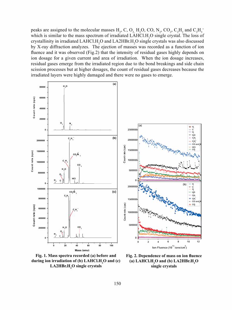
Ion Irradiation on single crystals has induced some significant modifications in the properties of the crystals such as refractive index, dielectric constant, nonlinear optical property and mechanical stability. Hence to understand the cause of this property changes in irradiated crystals, residual gas analyzes were carried out for L-Arginine monohydrochloride monohydrate and L-Arginine dihydrobromide monohydrate single crystals to which were irradiated with 100 MeV Ag8+ ions at different ion fluence ranging from 7.9 x 10¹⁰ to 1.19 x 10¹⁴ ions/cm2. This residual gas analyzes provide information about the ion-single crystal interactions. The gases evolved from Ag8+ ion irradiated LAHCl.H2O and LA2HBr.H2O single crystals were analyzed by quadrupole mass analyzer (QMA). Spectra were recorded before and after irradiation to identify the gases coming out of the samples during irradiation. No molecular species of mass more than 60 amu was detected. Out of the detected gases, prominent ones were analyzed as a function of ion fluence. Fig. 1(a) shows the mass spectrum recorded before ion irradiation for the evacuated chamber. The main constituents of vacuum are H2O and N2 molecules. Spectrum of residual gases released from LAHCl.H2O during irradiation is presented in Fig. 1(b). The mass spectrum is characterized by the additional number of peaks (masses) H2, C, O2, H2O, CO, N2, HCl, CO2 and the dominant peaks are hydrocarbons such as C2H2 and C2H3
+. The reasons for the ejection of these molecular species are the bond breaking and side chain scission processes [1,2] taking place during ion irradiation. These bond breakings and side chain scission processes in LAHCl single crystals during ion irradiation are explained by Fourier transform infrared spectra. Fig. 1(c) presents the mass spectrum of LA2HBr.H2O and the
150
peaks are assigned to the molecular masses H2, C, O2, H2O, CO, N2, CO2, C2H2 and C2H3+
which is similar to the mass spectrum of irradiated LAHCl.H2O single crystal. The loss of crystallinity in irradiated LAHCl.H2O and LA2HBr.H2O single crystals was also discussed by X-ray diffraction analyzes. The ejection of masses was recorded as a function of ion fluence and it was observed (Fig.2) that the intensity of residual gases highly depends on ion dosage for a given current and area of irradiation. When the ion dosage increases, residual gases emerge from the irradiated region due to the bond breakings and side chain scission processes but at higher dosages, the count of residual gases decreases because the irradiated layers were highly damaged and there were no gases to emerge.
Fig.1.Massspectrarecorded(a)beforeandduringionirradiationof(b)LAHCl.H2Oand(c)
la2HBr.H2Osinglecrystals
Fig.2.Dependenceofmassonionfluence(a)LAHCl.H2Oand(b)LA2HBr.H2O
singlecrystals

151
To observe the property changes in irradiated LAHCl single crystals, the crystals were irradiated with 100 MeV Ag8+ ions and 50 MeV Li4+ ions. These ions were irradiated with different ion fluence (1 x 10¹¹, 3 x 10¹¹, 5 x 10¹¹ and 1 x 10¹² ions/cm2). Irradiation induced changes in dielectric property, second harmonic generation (SHG) efficiency and mechanical stability of LAHCl single crystals were studied. The dielectric constant and mechanical stability of irradiated LAHCl single crystals were high at low fluence (1 x 10¹¹ ions/cm2) and decrease at high ion fluence (3 x 10¹¹, 5 x 10¹¹ and 1 x 10¹² ions/cm2). This has been explained by the density changes in the irradiated samples. The SHG efficiency of irradiated LAHCl single crystals were low compared to pristine LAHCl. This may be due to the increased defects in the irradiated LAHCl which act as scattering centers and decreases the SHG output.
reFerences
[1] V. Picq, J.M. Ramillon, E. Balanzat, Nucl. Instr. and Meth. in Phys. Res. B 146 (1998) 496.[2] Changlong Liu et al. Nucl. Instr. and Meth. in Phys. Res. B 169 (2000) 72.
5.2.3 Swift heavy ion (SHI) induced mixing and gas evolution study in Ni-teflonsystem
Jai Prakash1, A. Tripathi2, S. A. Khan2, J. C. Pivin3, Jalaj Tripathi1, Sarvesh Kumar4 and D. K. Avasthi2
1Department of Chemistry, M.M.H (P.G) College, Ghaziabad 2Inter University Accelerator Centre, Aruna Asaf Ali Marg, New Delhi 3CSNSM, IN2P3-CNRS, Batiment 108, F-91405 Orsay Campus, France 4Department of ASH (Physics), C.I.T.M., Aravali Hills, Sector-43, Faridabad
Swift Heavy ion (SHI) when passing through a material, results in materials modification by inducing high degree of localized electronic excitation. The magnitude of the effect on the target material depends mainly on the electronic energy loss of the ion and also on materials properties [1, 2]. The chemical changes induced by any kind of ionizing radiation in polymer (e-, UV, ions) generate ions or free radicals that initiate the molecular fragmentations, chain scissioning, cross-linking and formation of unsaturated groups [3, 4]. Avasthi et al. have reported that SHI produces a cylindrical molten zone termed as ion track in polymer by breaking of bonds with stimulated evolution of gases [5]. The bond breaking within polymer chains and reaction with the metal resulting in chemical bond formation during the irradiation may become responsible for the mixing in metal polymer system. In the present work we have studied the SHI induced interface mixing in Ni-teflon system.
100 nm thin film of Ni was deposited on Teflon (PTFE) using e-beam evaporation technique in ultra high vacuum (~10-7 torr) chamber. High energy ion beam irradiation was
152
carried out using 15 UD Pelletron accelerator at Inter-University Accelerator Centre (IUAC), New Delhi. 120 MeV Au ions were used at fluences varying from 1×10¹² to 5×10¹³ ions/cm2 for irradiation.
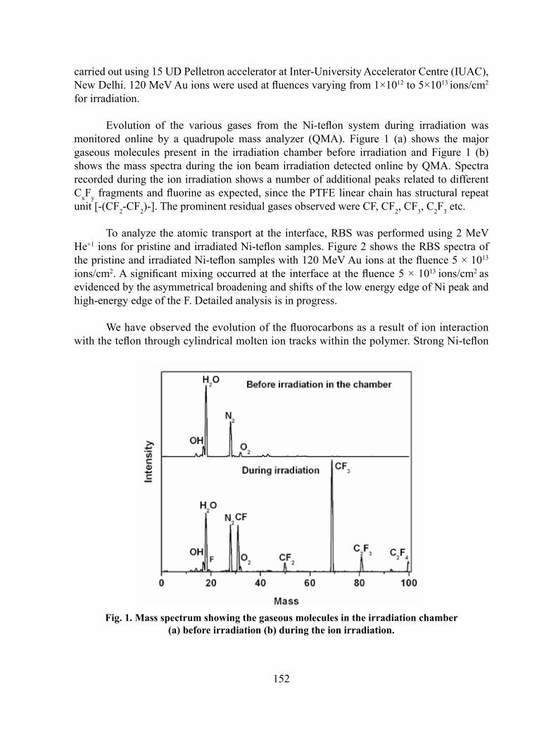
Evolution of the various gases from the Ni-teflon system during irradiation was monitored online by a quadrupole mass analyzer (QMA). Figure 1 (a) shows the major gaseous molecules present in the irradiation chamber before irradiation and Figure 1 (b) shows the mass spectra during the ion beam irradiation detected online by QMA. Spectra recorded during the ion irradiation shows a number of additional peaks related to different CxFy fragments and fluorine as expected, since the PTFE linear chain has structural repeat unit [-(CF2 -CF2)-]. The prominent residual gases observed were CF, CF2, CF3, C2F3 etc.
To analyze the atomic transport at the interface, RBS was performed using 2 MeV He+1 ions for pristine and irradiated Ni-teflon samples. Figure 2 shows the RBS spectra of the pristine and irradiated Ni-teflon samples with 120 MeV Au ions at the fluence 5 × 10¹³ ions/cm2. A significant mixing occurred at the interface at the fluence 5 × 10¹³ ions/cm2 as evidenced by the asymmetrical broadening and shifts of the low energy edge of Ni peak and high-energy edge of the F. Detailed analysis is in progress.
We have observed the evolution of the fluorocarbons as a result of ion interaction with the teflon through cylindrical molten ion tracks within the polymer. Strong Ni-teflon
Fig.1.Massspectrumshowingthegaseousmoleculesintheirradiationchamber (a)beforeirradiation(b)duringtheionirradiation.

153
mixing is observed attributing to the fact that ion beam induced chemical reactions within ion tracks enhance the mixing process. Chemical reactions occur in the hot zones around the ions path in Ni film and molten cylindrical ion tracks in polymer between the metallic nickel and reactive fluorocarbon species produced during the irradiation from Ni-teflon system. Formation of the (-CFNi-) complex and NiF2 compound as observed in ESCA study (not shown here), support the chemical reactions and subsequent mixing in Ni-teflon system.
reFerences
[1] Z. G. Wang, C. Dufour, E. Paumier, M.Toulemonde. J phys: Condens Matt 6 (1994) 6733.[2] M. Toulemonde, C. Dufour, E. Paumier. Acta phys Polonica A 9 109 (2006) 3.[3] U. Lappan, U. Geibler, L. Haubler, K. Jehnichen, G. Pompe, K. Lunkwitz. Nucl Instr Meth B 185
(2001) 178. [4] A. Oshima, K. Murata, T. Oka, N. Miyoshi, A. Matsuura, H. Kudo, T. Murakami, E. Katoh, M. Washio,
Y. Hama. Nucl Instr Meth B 265 (2007) 314.[5] D. K. Avasthi, J. P. Singh, A. Biswas, S. K. Bose. Nucl Instr Meth B 146 (1998) 504.
5.2.4 SwiftHeavyIonInducedModificationinTe/BiBilayerSystem
Th.Diana1, H.Nandakumar Sarma1, D.C.Aggrawal2, P.K.Kulriya2, S.K.Tripathi3, J.C.Pivin4 and D.K.Avasthi2
1Department of Physics, Manipur University, Imphal 2Inter-University Accelerator Center, New Delhi 3Department of Physics, Panjab University 4CSNSM, IN2P3-CNRS, Batiment 108, 91405 Orsay Campus, France
In this report, we investigate the possibility of mixing in the Bi/Te bilayer system on irradiation by swift heavy ions. Ion beam mixing, most likely, occurs if the ion beam creates track in one of the layers. Track formation is already reported in bismuth.
Te/Bi/glass system is irradiated with 100 MeV Ag7+ ions using 15 UD pelletron at IUAC, New Delhi. The ion fluences were in the range of 1012-1014 ions/cm2and current of 10 particle nA. The irradiated as well as pristine samples were characterized by grazing incidence XRD technique for the identification of phase formation at the interface using Bruker D8 advance XRD in the scan range of 150-600 and scan speed of 0.5 deg/min at IUAC, New Delhi. Figure 1 shows the GIXRD plots of pristine and irradiated samples of fluences 1014 ions/cm2. As-deposited film shows Te to be the main contributing peak and Bi may get amorphised. Irradiated film showed Bi2Te3 and Te. It can be clearly observed that Te peak intensity gets lowered while some get disappeared showing Te getting absorbed in the system.

154
The RBS spectra of as-deposited and irradiated Te/Bi under the fluences 1014 ions/cm2 are given in Fig.2. The analysis of the spectra was performed using the RUMP program. The program allows the simulation and fitting of composition profile of the elements involved. The analysis shows that rigorous mixing takes place on SHI irradiation of the bilayer. However the effect of roughness leads to an additional broadening of the features present in the energy spectrum. Therefore, further analysis was done with atomic force microscopy. Detailed analysis is in progress.
Fig.1.XRDplotsofpristineandirradiatedsamples
Fig.2.RBSspectraofpristineandirradiated(Agion,e14ions/cm2)samples

155
5.2.5 SwiftheavyioninducedmodificationinIn/Tebilayerthinfilms
R.Sathyamoorthy1, D.K.Avasthi2, K.Asokan2 and D.Kabiraj2
1Department of Physics, Kongunadu Arts & Science College, Coimbatore 2Inter-University Accelerator Centre, Aruna Asaf Ali Marg, New Delhi
III-VI compound semiconductors receive great attention due to its applications in memory devices, switching devices, gas sensors, hybrid solar cells etc. Among these compounds, In2Te3 is a promising material for solar cell applications, gas sensors, pressure transducers etc. Indium telluride thin films have been prepared by various methods like vacuum evaporation [1], flash evaporation [2], sequential thermal evaporation [3], co-evaporation [4], etc. However, not much work has been carried out in In/Te bilayer system. Thus, it is of great interest to investigate the possibility of mixing in the In/Te bilayer system by SHI. In order to study SHI induced mixing in In/Te bilayer, we have deposited In and Te thin films over well-cleaned glass substrate by thermal evaporation at Ar atmosphere in room temperature. We have chosen the elemental ratio of In and Te in relevant proportions [Te/In]=3/2 in order to form In2Te3. Film thickness are measured and controlled by in-situ quartz crystal thickness monitor. Post annealing of prepared samples at 300°C in Ar atmosphere yields In2Te3. The samples are irradiated with 100 MeV Ag and 100 MeV Si ions under the fluences of 1×10¹², 3×10¹², 5×10¹², and 1×10¹³, 3×1013,5×1013 using 15 UD pelletron accelerator at IUAC, New Delhi. Post deposition annealing was carried out on irradiated films at 150°C in Ar atmosphere.
Pristine, annealed, irradiated and post annealed (after irradiation) samples are characterized by XRD technique with Cu Kα-radiation (1.54Å) using Bruker D8 advance XRD in the scan range of 20°-60° and scan speed of 0.5 deg/min at IUAC, New Delhi. The XRD results show that the irradiated sample has mixed phase of In2Te3 and In4Te3, where as the samples annealed after irradiation at 150°C yields In2Te3 alone. It reveals that SHI irradiation leads to the formation of In2Te3 at lower annealing temperature. From the optical analysis, it is observed that after irradiation the transmittance increases in the visible region. Further we need to take Rutherford Backscattering Spectroscopy, Atomic force microscopy and electrical conductivity measurements to study the elemental composition, surface morphology and electrical properties.
reFerences
[1] R.Rousina & G.H. Yousefi, Materials Letters 9 (1990) 263-265.[2] R.R.Desai, D.Lakshminarayana, P.B.Patel, P.K.Patel & C.J.Panchal, Materials Chemistry and Physics
94 (2005) 308-314.[3] M.Emziane, J.C. Bernede, J,Ouerfelli, H.Essaidi & A.Barreau, Materials Chemistry and Physics 61
(1999) 229-236.[4] N.Guettari, C.Amory, M.Morsli, J.C.Bernede & A.Khelil, Thin Solid Films 431-432, (2003) 497-501.

156
5.2.6 SwiftheavyioninducedmixingatMn/Siinterface
Reena Verma1, Garima Agarwal1, Renu Dhunna1 D. Kabiraj2 and I.P. Jain1
1Centre for Non-Conventional Energy Resources, University of Rajasthan, Jaipur 2Inter University Accelerator Center, Aruna Asif Ali Marg, New Delhi
Metal silicides are compounds formed at metal/ Si interface exhibiting ohmic or Schottky contact and are of practical importance in device physics and technology. Metal silicides have found their application in various fields such as, high temperature devices [1], microelectronic devices, where they are used as interconnects for VLSI, ULSI [2,3] due to their low resistivity , heat resistance and good thermal stability [4]. Amongst the various transition metal silicides, manganese silicides shows different phases e.g MnSi, Mn5Si2, Mn5Si3, Mn6Si, Mn4Si7, Mn14Si23, Mn27Si47, and Mn15Si26.
The films of a-Si/Mn/a-Si have been deposited on Si [100] substrate of 1-10 Ω-cm resistivity. The n-Si wafer have been degreased by successively boiling in Trichloroethylene (TCE), acetone and Isopropyl alcohol, and rinsed in deionised water. Thereafter the wafer was dried in clean air and loaded into a vacuum chamber (~10-8 Torr) for metallization using electron beam evaporation technique. This system was irradiated by 120 MeV Au ions at fluence of 1x10¹⁴ ions/ cm2 at RT. The virgin and irradiated samples were characterized using GIXRD and AFM studies at IUC, Indore.
Compound formation at the interface as a result of mixing at the Mn/Si interface has been investigated by X-ray diffraction data recorded at an incidence angle of 0.50. Fig 1 shows the XRD pattern of the un-irradiated Si/Mn/Si structure which shows two clear distinct peaks corresponding to Mn [221] and Si [103] and Fig 2 is the XRD studies of irradiated system which shows the peaks corresponding to Mn5Si2 due to mixing at the interface.
Fig.2.GIXRDcurveofirradiated si/Mn/si
Fig.1.GIXRDcurveofpristinesi/Mn/si

157
Surface morphology of the Si/Mn/Si system was investigated by AFM micrographs shown in Fig 3 and Fig 4, both for unirradiated and irradiated samples. It is observed that the average grain size and surface roughness have been increased after irradiation. The calculated values are 29nm and 0.957nm for unirradiated and 69nm and 3.329nm for irradiated samples at 1x10¹⁴ ions/cm2 fluence.
Fig.4.AFMmicrographoftheirradiated si/Mn/si
Fig.3.AFMmicrographofthepristine si/Mn/si
Present work reports the SHI-induced interface mixing at a-Si/Mn/a-Si interface system irradiated using 120 MeV Au ions at a fluence of ~ 1014 ions/cm2. GIXRD measurements reveal the formation of granular silicide phase of Mn5Si2 due to ion beam induced mixing at the interface.
reFerences
[1] A.K. Vasudeven, J.J. Petrovie, Mater. Sci. Eng. A 155 (1992) 1.[2] S.P. Murarka, Mater. Sci. Eng. R 19 (1997) 87.[3] J. Li, Y. Shancham-Diamand, J.W. Mayer,Mater. Sci. Rep. 9 (1992) 1.[4] S.P. Murarka, J. Vac.Sci. Technol. 17 (1980)775.
5.2.7 StructuralmodificationsofCarbonnanotubesbyswiftheavyionirradiation
Kiran Jeet1, V. K. Jindal1, L. M. Bharadwaj2, F.Singh3 and Keya Dharamvir1
1Dept. of Physics and Centre for Adv. studies in Physics, Panjab University, Chandigarh
2Biomolecular Electronic and Nanotechnology Division, Central Scientific Instruments Organisation, Chandigarh
3Inter University Accelerator Centre, Aruna Asaf Ali Marg, New Delhi
Irradiation of carbon based materials such as fullerenes, single-walled carbon nanotubes (SWCNTs) and multi-walled carbon nanotubes (MWCNTs) with beam of

158
energetic particles (ions or electrons) is emerging as a potential tool for modifying their properties at atomic as well as at nanoscale. It is a general belief that the irradiation of highly energetic ions /electron (energy of the order of MeV) induces disorder in the material but recent experiments on irradiation of carbon based nanostructures by energetic ions have shown striking evidences of reordering of the system [1-3]. Motivated by these observations, we study the effect of irradiation of SWCNT and MWCNT with swift heavy ions of C of energy 55 MeV and MWCNT samples with Au ions of energy 120 MeV.
Thin film samples of carbon nanotubes were deposited using a chemical route. The thicknesses of the films were found to be 15 micron for SWCNTs and 22 microns for MWCNTs. These films were irradiated with 55 MeV carbon ion beam in a fluence range 3 x10¹¹ to 1x10¹⁴ ions /cm2 and 120 MeV Au ion beam in a fluence range 3x10¹¹ to 3x10¹³ ions /cm2. The irradiated samples were characterized using Raman Spectroscopy. Modifications of the disorder mode (D mode) and the tangential mode (G mode) under different irradiation fluences were studied in detail. In order to get the qualitative estimate of the modification occurring in CNT systems due to irradiation, we plot the variation of disorder parameter (I(D)/I(G)) as a function of ion fluence (shown in Fig 1). The Raman results indicate the interesting phenomenon of healing or annealing of CNTs due to carbon ion beam irradiation. At lower values of fluence, the annealed process appears to begin and persists for quite a good range of fluence values but as the irradiation time increases (at 1x10¹⁴ ions /cm2) the system begins to amorphize.
The possible mechanism of the annealing is via rearrangement of the bonds. When an energetic ion passes through the materials, it heats up the material along the ion track by transferring its Se (electronic energy loss), leading to electron phonon coupling, which then generates the thermal vibrations in the atoms. This causes annealing of the material in the vicinity of the ion track.
Fig.1.Variationofdisorderparameter((I(D)/I(G)))asfunctionofirradiationfluence for(a)SWCNTssamplesirradiatedwithCarbonionsand(b)MWCNTs
samplesirradiatedwithAuions.
Irradiation fluence Irradiation fluence

159
reFerences
[1] A. Dunlop, P. M. Ossi, and S. Della-Negra, Phys. Rev. B 76 (2007) 155403.[2] A. Kumar, D. K. Avasthi, J. C. Pavin, and P. M. Koinkar, Appl. Phys. Lett.92, (2008) 221904-1-
221904-3.[3] 5. Y. Yao, M. Y. Liao, , Th. Kohler, Th. Frauenheim, R. Q. Zhang, Z. G. Wang, Y.Lifshitz and S. T. Lee,
Phys. Rev. B 72, (2005) 035402.
5.2.8 StructuralandAFM/MFMstudiesofnickelnanostructuresembeddedinAl2O3 matrix
Aditya Sharma1, Arvind Kuma2, Rakesh Dogra2, Mayora Varshney 1, K.D.Verma1, S. Chopra3, Devrani Devi3, and Ravi Kumar3
1Material Science Research Laboratory, Department of Physics, S.V.College, Aligarh 2Beant College of Engineering and Technology, Gurdashpur 3Inter University Accelerator Center, Aruna Asaf Ali Marg, New Delhi
This work reports the formation and characterization of Ni nanostructures embedded in Al2O3 (sapphire) matrix. Single crystals of sapphire were implanted with 80 KeV negative Ni ions at a fluence of 7 × 10¹⁶ ions cm−2 and post annealed in air at 600 °C for 4 hrs. X-ray diffraction, AFM/MFM and UV-visible absorption, investigations confirmed the formation of embedded nickel nanostructures at a fluence of 7 × 10¹⁶ ions cm−2.
Figure 1(a) and 1(b) shows the XRD patterns of single crystal α-Al2O3 and 80 KeV Ni- ion implanted Al2O3 with the implantation dose of 7x10¹⁶ ions cm-2 (annealed at 600oC for 4 hrs), respectively. It is clear from the figures that all the diffraction peaks have been observed for α-Al2O3 with highest intense peak of (006) plane, while a new broad peak appeared at 2θ = 44.55o in the implanted sample. This diffraction peak (2θ = 44.55o) has been identified to be of Ni (111), which is near to the reflection of bulk nickel. The corresponding average size of the nickel nanoparticles, calculated using the Scherrer formula is ~8.2 nm. Figure 2(a) and 2(b) show the AFM images taken at room temperature for the pristine and Ni-implanted Al2O3. It is clearly seen by the AFM that the surface of Al2O3 is very smooth, having surface roughness value of ~1.7 nm, while surface roughness has been estimated to be ~12.5 nm in the Ni implanted sample. To check the magnetic domain structures on the surface of implanted samples, systematic MFM measurements have been performed at the 30 nm lift height. It is evident from fig. 2 (a) that the single crystal of α-Al2O3 does not show any magnetic contrast. On the other hand, the figure 2(b) indicates the presence of magnetic contrast, due to the formation of Ni nanostructures in Al2O3 matrix. The magnetic domains are oriented in one direction along the plane of the single crystal of Al2O3. These results strengthen our XRD results for the growth of Ni nanostructures embedded in Al2O3 matrix with an average size of ~8 nm.

160
5.2.9 IonirradiationeffectonnanocrystallinethinfilmsofPbS
N Choudhury1, F Singh2 and B K Sarma1
1Department of Physics, Gauhati University, Guwahati 2Inter University Accelerator Centre, New Delhi
Nanocrystalline PbS are irradiated with 100 MeV Ni8+ ions with three different fluences 1 x 10¹¹, 1 x 10¹² and 1 x 10¹³ ions cm-2. There are only few reports on swift heavy ion (SHI) induced modification of optical properties of PbS [1]. SHI irradiation technique is unique due to its capability to deposit very high energy in a localized area of the material and thereby attaining spatial selection while modifying its properties [2].
Figure 1 shows the XRD spectra of pristine and SHI irradiated nanocrystalline PbS. The average grain size increases from 11 nm for the pristine sample to 17 nm for the sample irradiated at the fluence of 1x10¹¹ ions cm-2 and remains almost constant for the higher fluences. This increase in the particle size with irradiation due to energy induced coalescence of the grains. The increase in peak intensity and grain size indicates an improvement of crystallinity of the samples. The X-ray diffraction peak position (2θ = 25.7°, 29.9°, 42.8°, 50.7° and 53.3°) has remained fixed for all PbS samples irradiated with different fluences and is same for pristine sample. This indicates absence of strain in the nanocrystalline samples after irradiation. Figure 2 shows PL spectra of pristine and SHI irradiated nanocrystalline PbS. It is observed that the pristine samples show minimum PL intensity whereas it increases for irradiated samples. This is obvious as the defect concentration is expected to increase after irradiation [3].
Fig.1.XRDpatternsof(a)Pristineand(b)Ni-implantedAl2O3
Fig.2.MFMimagesof(a)Pristineand(b)Ni-implantedAl2O3

161
reFerences
[1] S Chowdhury, S K dolui, D K Avasthi and A Choudhury, Indian J. Phys. 79 (2005) 1019.[2] V V Ison, A Ranga Rao, V Dutta, P K Kulriya, D K Avasthi and S K Tripathi, J. Appl. Phys. 106 (2009)
023508.[3] K Schrawat, F Singh, B P Singh and R M Mehra, J. Luminesc. 106 (2004) 21.
5.2.10SHIeffectsonGe+SiO2compositefilmspreparedbyRFsputtering
N Srinivasa Rao1, N Sathish1, G Devaraju1, V Saikiran1, A P Pathak1, P K Kulriya2, S A Khan2 and D K Avasthi2
Fig.1.XRDspectraofpristineandirradiatedPbS.
Fig.2.PLspectraofpristineandirradiatedPbS

162
1School of Physics, University of Hyderabad, Central University, Hyderabad 2Inter University Accelerator Centre, P.O.10502, New Delhi 110 067
The structural, optical and electronic properties of low dimensional, indirect band gap materials have been investigated extensively over the past years. Particularly, the effective Bohr radius of the exciton in Ge is larger than that in Si. Hence, it is easier to change the electronic structure around the band gap of Ge than Si due to its larger exciton Bohr radius. The present work investigates the structure of the Ge nanocrystals grown by RF magnetron sputtering using swift heavy ion irradiation.
SHI irradiation was done at room temperature with 150 MeV Ag12+ ions with fluences varying from 3X10¹² to 3×10¹³ ions /cm2 using the 15 MV pelletron at IUAC. To avoid heating of the samples a low beam current was maintained. Finally these films were characterized by Rutherford Backscattering Spectrometry (RBS), X-ray diffraction (XRD) and Transmission Electron Microscopy (TEM).
Fig.1.(a)XRDspectraofdepositedandirradiatedsamplesand(b)TEMimageofirradiatedsamplewith150MeVAgwithfluence3x1013ions/cm2.
The X-ray diffraction (XRD) spectra of the as-deposited and ion irradiated samples are shown in figure 1(a). In the case of as-deposited sample, no peak is observed, whereas the irradiated samples show crystalline planes, which indicates the formation of nc-Ge. The TEM image of irradiated sample with 3x10¹³ ions/cm2 fluence shows that the average crystallite size was around 18 nm.
5.2.11 StudyingdeformationbehaviorofSinanospringsbylowandhighenergyionbeamsandinvestigatingtheeffectontheirmechanicalstiffness
Rupali Nagar1, C Patzig2, C. Khare2, B Rauschenbach2, D Kanjilal3, B R Mehta1 and J P Singh1

163
1 Department of Physics, Indian Institute of Technology Delhi, Hauz Khas, New Delhi
2Leibniz-Institut für Oberflächenmodifizierung e.V. Leipzig Permoserstraße 15 D- 04103, Leipzig, Germany 3 Inter University Accelerator Centre, Aruna Asaf Ali Road, New Delhi
Ion beam irradiation has been used for doping, improving properties of materials, alloying and synthesis of nanostructures. However, bombardment with energetic ions can also cause severe damage to the target material. Ion hammering effect (IHE) is one such phenomenon in which the target undergoes a contraction along the ion beam direction and expansion in a lateral direction. [1-3] It was the objective of the present research work to identify the probable factors and parameters that lead to IHE. For this purpose vertically standing Si nanosprings grown on SiO2 spheres[4] were irradiated under the following conditions.
(i) `Low energy (LE): 1.2 MeV Ar+8 ions, room (RT) and liquid nitrogen temperature (LT).
(ii) High energy (HE): 100 MeV Au+7 ions, RT and LT.
After irradiation, the samples were characterized in top-view and cross-sectional view scanning electron microscopy (SEM). Fig. 1 shows the prototype of the pristine sample along with the samples irradiated under different conditions and different ion fluence marked against them.
Fig.1.Cross-sectionalSEMmicrographsofSinanosprings irradiatedunderdifferentconditions.
It was observed that irradiation at RT resulted in lesser deformation as compared to LT irradiation. The data also provides indications that nuclear losses play some role in deformation, a fact which has been overlooked by researchers in the past. Higher ion fluence of 5 x 10¹⁶, however, lead to melting and flow of silicon and destroyed the nanosprings completely. On the other hand, nanosprings irradiated at 1 x 10¹⁷ under LE-LT conditions deform but retain their identity. This aspect is being further investigated. For high energy irradiation, where electronic losses are dominant, the deformation is less at RT as compared to LT irradiation. At higher irradiation temperatures, the mobility of defects formed during irradiation is high. The defects may therefore anneal out resulting in lesser deformation as

164
compared to LT irradiation. Also, immediately after the spike phase is over, the viscosity of Si at RT will be higher as compared LT, and the recovery of deformation during the spike phase will be relatively faster.
After irradiation, the mechanical stiffness of the Si nanosprings was investigated by atomic force microscope based force-distance spectroscopy.[5,6] Interestingly, the mechanical stiffness of the nanosprings shows a logarithmic dependence on energy density (ε ~10 keV nm-3) deposited in the target material. Beyond this value of energy density, the nanosprings deform to a large extent. The change in the stiffness of the nanosprings then occurs due to the change in their dimensions. Fig. 2 plots this dependence for LE-LT and HE-LT samples. Therefore, the energy deposited per unit volume is a common parameter that directly influences the stiffness in both cases of ion irradiation. The study indicates that higher surface-to-volume ratio of nanostructures and shape anisotropy can aid in delaying the deformation of nanostructures to some extent.
Fig.2.NormalizedstiffnessofSinanospringsplottedasafunctionofε.
reFerences
[1] H Trinkaus, I A Ryazanov, Phys. Rev. Lett. 74 (1995) 5072. [2] H. Trinkaus, J. Nucl. Mater 223 (1995) 196.[3] S Klaumünzer, Nucl. Instr. Meth. Phys. Res. B. 215 (2004) 345.[4] C Patzig, B Rauschenbach, W Erfurth, A Milenin, J. Vac. Sci. Technol. B 25 (2007)
833.[5] R. Nagar, C Patzig, B Rauschenbach, V. Sathe, D. Kanjilal, B. R. Mehta, J. P. Singh,
J. Phys. D: Appl. Phys. 42 (2009) 145404.[6] R. Nagar, D. Kanjilal, B. R. Mehta, J. P. Singh, Nucl. Instr. Meth. Phys. Res. B 267
(2009) 3617.

165
5.2.12Nanoscale surface engineering of single crystalline oxide substrates using ionbeams
Utpal S. Joshi1, B.V. Mistry1 and S.A. Khan2
1Department of Physics, School of Sciences, Gujarat University, Ahmedabad 2Inter University Accelerator Centre, Aruna Asaf Ali Marg, New Delhi
Surface reconstruction and modification of the commercially available single crystal oxide substrates are key issues for fabrication of devices [1]. Since the functional epitaxial thin film is in direct contact with the substrates, the surface properties of the substrates are expected to directly affect the characteristics of the device. Abnormal device behaviors such as shorting, unstable I –V characteristics, and damage on the surface of the top cathode contact after continuous operation of the device have been observed in, for example, OLEDs built on bare cleaned ITO surfaces [2]. We have used ion beam irradiation as a tool to modify the surface properties of three important oxide single crystalline substrates, namely, SiO2 (quartz), LaAlO3 (100) (LAO) and MgO (100). Double side polished single crystal plates of these substrates were irradiated by 50 MeV Li3+ ions at IUAC, New Delhi with a fluence ranging from 1x10¹¹ to 1x10¹³ ions/cm2 and were characterized by AFM and UV-Vis. spectroscopy.
Fig. 1(a, b, c) show the optical spectrographs and typical AFM images of pure and 50 MeV Li3+ ion irradiated SiO2, LaAlO3 and MgO single crystal substrates, respectively. As can be seen from the AFM images, in case of SiO2 (quartz) substrate, surface reconstruction is observed over a wide scan area of 5 µm x 5 µm. Surprisingly, the RMS surface roughness was found to decrease in the irradiated crystal of SiO2. The optical band showed a fluence dependence and was found to decrease from 4.8 eV to 4.1 eV when irradiation fluence increased from 1x10¹¹ to 1x10¹³ ions/cm2, as can be seen in fig. 1(a). Note that no significant decrease in the absorption (transmittance) was seen in the visible range upon SHI irradiation.
In case of LaAlO3 (100) single crystal wafers, the Li irradiation induced surface roughness, as can be seen in the AFM images of fig. 1(b). Here, the virgin sample, as received commercially from the MTI Corporation, USA, possess step and terrace type atomically smooth surface. The Li irradiation altered the surface morphology and the RMS roughness was found to increase to about 8.5 nm, which is larger than the LAO unit cell parameter. Interestingly, no shift in absorption band edge was seen for any of the ion fluence values. Further, the optical absorption values remained almost constant for any of the 50 MeV Li3+ ion fluence values, up to 1x10¹³ ions/cm2. The perovskite crystal structure of LAO may have role to play on the surface structure modification and observed optical properties. We are analyzing the results in detail.

166
Finally, we irradiated MgO (100) single crystal squares with 50 MeV Li3+ ions at different fluences and the AFM and optical spectra are displayed in fig. 1(c).
Like the SiO2, MgO also showed a surface reconstruction upon SHI irradiation and the RMS roughness was found to increase with incident ion fluence. The optical band gap observed to decrease from 4.35 eV to 4.12 eV.
The results are preliminary and are under investigations but they carry lot of promise to demonstrate the SHI as a tool to do nanoscale surface engineering of oxide substrates.
Fig.1.TypicalAFMimagesandUV-Vis.absorbancespectrographsof50MeVLi3+ionsirradiated(a)SiO2(b)LaAlO3and(c)MgOsinglecrystalsubstrates.AFMscan
rangeis5µmx5µmforalltheimages.

167
reFerences
[1] Nanostructured Thin Films and Nanodispersion Strengthened Coatings, 2004, J.S. Colligon, A. A. Voevodin et.al. (Editors), Springer, pp 297-306.
[2] J. R. Sheats, H. Antoniadis, M. Hueschen, W. Leonard, J. Miller, R. Moon, D.Roitman, and A. Stocking, Science 273, 884 (1996).
5.2.13OpticalPropertiesofZnO/PMMANanocompositesIrradiatedwithNi+8ion
Sarla Sharma1, Shweta Agrawal1, Subodh Srivastava1, Sumit Kumar1, B.Tripathi1, Fouran Singh2 and Y.K. Vijay1.
1Department of Physics, University of Rajasthan, Jaipur 2Inter-University Accelerator Center, Aruna Asaf Ali Marg, New Delhi
Swift heavy ion induced modifications in embedded polymer matrices have become an interesting area for scientific community due to changes in its structural, optical properties of the material. The influence of swift heavy ion (SHI) irradiation on structural and photoluminescence (PL) properties of ZnO nanocrystallites deposited into porous silicon (PS) templates by the sol–gel process was studied by R.G.Singh et al.[1].
In present work we have studied the changes in optical property of ZnO nanoparticles doped in PMMA matrix which has been irradiated by 100Mev Ni+8 beam at fluence 1x10¹¹ ions/cm2. Photoluminescence has been carried out to reveal surface emission. Characterization of these nanocomposites has been carried out using X-Ray diffraction (XRD), Optical absorbance and Photoluminescence. The structural analysis of as prepared ZnO nanoparticles was carried out.
The absorption spectra for pristine and irradiated with Ni+8 ions (100 MeV) were recorded. We observed that after irradiation absorption increases and absorption edge shift towards the higher wavelength which indicates the grain growth of ZnO nanoparticles after irradiation.
The AFM micrograph show that the surface of pristine nanocomposite polymer film is composed of dense grains but after irradiation it has been observed that most of ZnO particles agglomerate and form an uneven cluster structure.
ZnO bulk is known to be a good phosphor material. Photoluminescence of ZnO nanoparticles has been investigated by many researchers. The emission spectrum gives a broad peak at 540nm which is a green band which is attributed to the presence of an anion vacancy trap level within the forbidden gap. From these PL measurements we conclude that after irradiation with Ni+8 ions the luminosity of ZnO/PMMA nanocomposite enhanced as shown in Fig. 1. It may be due the change in microstructure of polymer film after irradiation.

168
Mercaptoethanol capped ZnO nanoparticles were prepared using a simple chemical route. ZnO nanoparticles were then dispersed in PMMA matrix to study the Luminescence properties. To enhance the luminosity of ZnO/PMMA nanocomposite we irradiated these samples with Ni+8 (100 MeV) and we found that after irradiation the luminosity of ZnO/PMMA nanocomposite enhanced which may be due to the change in microstructure of PMMA matrix after irradiation with swift heavy ion. We suggest that the redistribution of nano particles takes place when tracks are formed in the polymers due to SHI. These tracks of lower nano particle density in comparison to unirradiated regions are responsible for enhancement in the PL yield from the samples.
Fig.1.PLspectraforZnOnanocomposite(a)pristineZnO/PMMAnanocomposite(b)irradiatedZnO/PMMAnanocomposites
reFerence
[1] R.G.Singh et al Nuclear Instruments and Methods in Physics Research B 267 (2009) 2399–2402.
5.2.14TheEffectofIonBeamonPVDFcopolymer/LayeredSilicateNanocomposites
Vimal Kumar Tiwari1, Pralay Maiti1, D.K. Avasthi2 and P. K. Kulriya2
1School of Materials Science and Technology, Institute of Technology, BHU, Varanasi
2Inter University Accelerator Centre, Aruna Asaf Ali Marg, New Delhi
Non-reactive and technologically important poly(vinylidene fluoride-co-hexafluoro propylene) (HFP) has similar crystalline structure to that of poly(vinylidene fluoride) (PVDF). The degree of crystallinity of the HFP is greatly reduced, while the flexibility and chemical resistance are enormously enhanced when compared with pure PVDF. We synthesized HFP

169
nanocomposites with layered silicate via melt extrusion route. HFP crystallizes in α-phase in bulk but nanoclay induces the piezoelectric β-phase in HFP nanocomposites. From the XRD and TEM, we found that HFP forms intercalated and partially exfoliated nanostructure depending on its concentration (fig. 1). The irradiation of swift heavy ions (SHI) of Si7+ with 80 MeV on HFP and nanocomposites has been studied in a wide range of fluences from 1×10¹⁰ to 5×10¹² ion-cm-2. XRD and DSC results show that amorphization takes place after irradiation of swift heavy ions in HFP and its nanocomposites. The change in heat of fusion of HFP is relatively lower in nanocomposites as compared to pristine HFP. The piezoelectric β-phase is retained in nanocomposites after SHI irradiation indicating that the nanocomposites can be used as radiation resistant piezoelectric materials at high temperature. We have performed qualitative and quantitative analysis of surface roughness of HFP and its nanocomposites after SHI irradiation. The effect of irradiation on HFP is severe on the surface topography while no significance changes have been observed in nanocomposites even at higher fluence (fig. 2). We confirmed that chain session is more in pristine HFP but significant crosslinking occurred in nanocomposites after the SHI irradiation even though both the processes occurred simultaneously in pure HFP as well as in nanocomposites by using sol-gel analysis and GPC studies.
Fig. 1. X-raydiffractionpatternsoforganicallymodifiedclay,pureHFP
anditsnanocomposites
Fig. 2. AFMimagesofHFP and NC4thinfilmbeforeandafterSHI irradiation at indicated
fluenceobtainedintappingmode
5.2.15SHI irradiation effects on optical and electrical properties of PPy-SnO2 nanocomposites
Smritimala Sarmah1, A. Kumar1and P.K. Kulriya2
1Materials Research Laboratory, Dept. of Physics, Tezpur University, Tezpur, Assam 2 Inter University Accelerator Centre, Aruna Asaf Ali Marg, New Delhi
There are a few reports on SHI irradiation induced modification of conductivity, optical and structural properties of metal oxide dispersed conducting polymer nanocomposites. In

170
this work, tin oxide (SnO2) nanoparticles were dispersed in conducting polypyrrole matrix by in-situ chemical oxidative polymerization process. The films of PPy-SnO2 nanocomposite were irradiated with 90 MeV O7+ ions at different fluences of 5×10¹⁰, 1×10¹¹, 5×10¹¹ and 1×10¹² ions/cm2.
Fig.1 shows the XRD patterns of pristine polypyrrole and PPy-SnO2 nanocomposites before and after irradiation at different fluences. XRD patterns of pristine PPy shows a characteristic broad peak at 2θ = 24o [1]. The crystalline peaks of PPy-SnO2 nanocomposite
Fig.1. XRDspectraof(a)unirradiatedPPy-(b)unirradiatedPPy-SnO2nanocompositeand(c-e)irradiatedPPy-SnO2nanocompositeatfluences5×1010,1×1011and1×1012ions/cm2
respectively.
Fig.2. PLspectraofPPy-SnO2 nanocomposites(a)beforeirradiationand(b-e)afterirradiationatfluences5×1010,
1×1011,5×1011and1×1012ions/cm2.
Fig.3TemperaturedependenceofdcconductivityofPPy-SnO2nanocomposite(a)beforeirradiationand(b-e)afterirradiation
atfluences5×1010,1×1011,5×1011 and1×1012ions/cm2
Fig.4FrequencydependenceofacconductivityofPPy-SnO2nanocomposite
beforeand(b-e)afterirradiation atfluences5×1010,1×1011,5×1011
and1×1012ions/cm2.

171
at 2θ values of 26.4o (110), 33.8o (101), 35.6o (200) and 51.8o (211) can be indexed to the tetragonal rutile structure of tin oxide. Upon irradiation of PPy-SnO2 nanocomposite, the intensity of the peak at 2θ = 24o increases at fluence ≥ 1×10¹¹ ions/cm2 as shown in Fig.1.This can be attributed to increased crystallization due to stacking and ordering of PPy chains along c direction with slight inclination against the direction perpendicular to the polymer chain direction (b direction) possibly due to a strong repulsion between the adjacent pyrrole rings upon SHI irradiation [2].
The photoluminescence intensity of the Polypyrrole-SnO2 nanocomposite increases with the increase of ion fluence (Fig.2). This can be attributed to increased thermal detrapping of charge carriers with the increase of fluence upon SHI irradiation [3]. As the concentration of defects increases with the increase in irradiation fluence, the radiative transition rate increases resulting in increased PL efficiency. Moreover fragmentation caused by SHI irradiation increases the density of grain boundaries, which also increases the PL emission intensity [3].
The dc electrical conductivity is found to increase with the increase of fluence as shown in Fig.3. This can be attributed to the creation of defects in the molecular structure of the polymer chains by SHI irradiation as charge accumulation takes place at these sites. The increase in crystallinity of the polypyrrole film also contributes to the increase in conductivity after irradiation due to decreased scattering of charge carriers. The dc conductivity (σdc) versus temperature behaviour can be fitted as one dimensional variable range hopping model following Mott’s T-1/2
law [4]
(1)
where σ0 is the high temperature limit of conductivity and T0 is the characteristic temperature that determines the thermally activated hopping among localized states at different energies. γ depends on the dimensionality‘d’ of the hopping by the relation )1(1 d+=γ while for one dimensional variable range hopping, d=1.
The AC conductivity σ (ω) as a function of frequency at room temperature for PPy-SnO2 nanocomposites before and after irradiation with 90 MeV O7+ ions at the fluences of 5×10¹⁰, 1×10¹¹, 5×10¹¹ and 1×10¹² ions/cm2 has been measured and is under analysis.
reFerences
[1] B Scrosati. Applications of Electroactive Polymers, Chapman & Hall, London, (1993).[2] Y. Nogami, J.-P. Pouget and T. Ishiguro, Synth. Met. 62, 257 (1994).[3] K. Sehrawat, F. Singh, B.P. Singh and R.M. Mehra, J. Lumin.106 21(2004).[4] N. F. Mott, J. Non-Cryst. Solids 1, 1 (1968).

172
5.2.16EffectofSHIirradiationonthermalandstructuralpropertiesofFe2O3/polymernanocomposites
N.L. Singh1, Dolly Singh1, Chaitali Gavade1 and Sangeeta1
1Department of Physics, The M. S. University of Baroda,Vadodara
Polymer nanocomposites with functional particles have much interest due to their cost effective processibility and high flexibility, rendering possible many applications such as micro wave absorbers, photovoltaic cells and smart structure. Inclusion of nanoparticles exhibit novel properties that significantly differ from those of corresponding bulk solid state owing to the different effects in terms of small size effect, surface effect, quantum size effect and macroscopic quantum tunnel effect.
PMMA was synthesized by solution polymerization technique. We were also synthesized Fe2O3 nanoparticles by chemical route. These particles were dispersed in PMMA by acetone solvent. The composite films of different concentrations (2%, 6% and 10%) of Fe2O3 powder in PMMA were prepared by casting methods. These films were irradiated with 50 MeV Li+3 ions at a fluence of 1012 ions/cm2.
Polyaniline was also synthesized by oxidative chemical polymerization technique. 0.2 M aniline hydrochloride oxidized with 0.25 M ammonium peroxydisulfate in aqueous medium. Film of the polymer was prepared by casting method. A smooth film hence obtained was doped by HCl. The free standing films of 1 cm2 were irradiated by 80 MeV C6+ ions at fluence of 1011 ions/cm2.
Fig. 1 Fig.2
Fig.1.DSCcurves(a)purePMMA(b)PMMA+10%Fe2O3 (pristine) (c)PMMA+10%Fe2O3 (irradiated),Fig.2:FTIRspectraof
(a)Polyaniline(Pristine)(b)Polyaniline(irradiated)

173
The thermal analysis was performed with differential scanning calorimetry instrument (S II EXSTAR 6000, DSC 6220) with the heating rate of 5 oC min-1. At the glass transition temperature, the weak secondary bonds that stick the polymer chains together are broken, and the macromolecule starts to move. Tg of the pure PMMA sample is observed at 72.5 oC and those of composite, pristine and irradiated samples at 77.4oC and 78.7oC respectively. This behavior probably arises from branching formed when islands of nanoparticles are bonded to different polymeric chains. This lowers the mobility of the chains, and as a result the glass transition temperature increases in the nanocomposites.
The functional groups of the polyaniline are identified from the pristine spectrum as follows, (a) aromatic C-H streching : 2917 cm-1, (b) aromatic amine group : 1272 cm-1, (c) protonation of aromatic amine : 1209 cm-1, (d) benzoid bands : 1438 cm-1(e) quinoid bands : 1560 cm-1 (f) undissociated acid : 875 cm-1. From FTIR spectrum of polyaniline, it is concluded that the polymer is in oxidized state. As, for emeraldine base form quinoid band and benzoid band have equal intensities and in the present spectrum benzoid band has greater intensity than quinoid band. From the comparison of FTIR spectra of pristine and irradiated samples, it is observed that upon irradiation the polymer gets oxidised, as the peak of benzoid band for irradiated sample is higher than the pristine. A reduction in the peak intensity of undissociated acid and an increase in the intensity of benzoid band have been observed, which supports the fact that oxidation of polymer takes place upon irradiation. The amplification in peak intensities is attributed to the cross-linking in polymer structure.
5.2.17SynthesisofMetalnanoparticlesusingionbeamsputtering
D. C. Agarwal1, Udai B. Singh1, S. A. Khan1, Aditi Dubey2, P. Kumar1, A. Tripathi1, N. K. Gohil3, and D. K. Avasthi1
1Inter-University Accelerator Centre, New Delhi 2Boston College for Professional Studies, Gwalior 3Centre for Biomedical Engineering, Ind. Inst. of Tech., New Delhi
Noble metal nanoparticles are of great importance because of their excellent optical properties showing the absorption in visible region. Research community has extensively investigated nanoparticles of noble metals for fundamental understanding and application in various fields. However, plasmonic nanostructures need more investigations to have better understanding of the nanoparticles size and their distribution. There are a large numbers of studies on synthesis of metal nanoparticles. Ion beam sputtering is one of the approaches to make metal nanoparticles and has several advantages over other methods like spatial selectivity, control of the nanostructure morphology, providing narrow size distribution and clean and reproducible process. Ion beam sputtering has been used to create exotic structures like ripples and nanodots on the surface [1-3] depending on beam parameters and material

174
properties. To the best of our knowledge, ion beam sputtering has not been used to produce plasmonic nanostructures.
In the present study, the effect of nuclear energy loss on formation of metal nanostructures has been studied. Metal (Au and Ag) thin film of thickness of 5 nm on glass and silica substrates have been deposited using thermal evaporation method.
Fig.1.AbsorptionspectraofSputteredAufilm(a)350keVArionbeam (b)1.5keVAratombeam
Au films were irradiated at different fluences by 350 keV Ar ions using low energy ion beam facility (LEIBF) [4] and 1.5 keV Ar atom beam at Inter University Accelerator Center (IUAC) New Delhi. UV-Vis spectra, shown in figure 1, of ion beam sputtered film show the signature of surface plasmon resonance peak at 520 nm, which indicates the formation of Au nanoparticles. However, films sputtered by 1.5 keV Ar atom beam show very broad weak signature of SPR of Au nanoparticles compared to 350 keV Ar ion sputtered films.
AFM micrographs support the results of absorption spectra and show the formation of Au nanoparticles.
Fig.2.AFMMicrographofgoldfilms(a)Pristine (b)350keVionbeamirradiatedatfluenceof3x1016ions/cm2

175
RBS analyses show that concentration of Au decreases with increasing ion fluence, which confirms sputtering induced formation of Au nanoparticles. We also infer from the RBS spectra that sputter yield reduces with increase in ion fluence.
Ag film on glass substrate has also been studied using ions of energy ranging from few keV to tens of MeV. Similar results have been observed as in case of Au nanoparticles.
In conclusion, present study demonstrated the formation of metal nanoparticles as a result of ion beam sputtering which can be utilized for various applications e. g. bio-medical applications and catalysis etc. The results give some indication about the ways to control particle size and its distribution.
reFerences
[1] P.K. Kulriya, A. Tripathi, D. Kabiraj, S.A. Khan and D.K. Avasthi, Nucl. Instr. and Meth. B 244 (2006) 95.
[2] I. Sulania, A.Tripathi, D. Kabiraj, S. Verma, D. K. Avasthi, J. Nanosci. & Nanotech. 8 (2008)4163.[3] S. Facsko, T. Dekorsy, C. Koerdt, C. Trappe, H. Kurz, A. Vogt, and H. L. Hartnagel, Science 285,
1551(1999). [4] P. Kumar, G. Rogrigues, P. S. Lakshmi, D. Kanjilal, R. Kumar, J. Vac. Sci. Technol. A 26 (2008) 97.
5.2.18SwiftheavyioninducedmodificationsofAu/a-Cnanocompositethinfilm
R. Singhal1, P. K. Kulriya1, D. Kabiraj1, F. Singh1 A. K. Chawla2, J. C. Pivin3, R. Chandra2, D. K. Avasthi1
1Inter University Accelerator Centre, Post Box No. 10502, New Delhi 2Institute Instrumentation Centre, Indian Institute of Technology Roorkee, Roorkee 3CSNSM, IN2P3-CNRS, Batiment 108, F-91405 Orsay Campus, France
Nanocomposite thin films containing noble metal nanoparticles are attractive because of their surface plasmon resonance (SPR). When metal nanoparticles are embedded in a matrix, not only the particles are stabilized but also prevented from agglomeration by Vander Waals forces. Matrices such as silica and alumina have been extensively used for incorporating noble metal nanoparticles due to their optical transparency in visible region [1]. But the large surface-to-volume ratio, tied to such small diameter particles, brings up the problem of instability of NPs due to their rapid oxidation, especially when they are embedded in oxide matrix [2]. Carbon based matrix are interesting, not only to protect the particles against oxidation but also the metal-carbon nanocomposite thin films show novel multi-functions in electronics, optics, magnetism and catalysis. In this paper, we report 120 MeV Ag ion irradiation induced modifications of gold/amorphous carbon (a-C) nanocomposite thin films.

176
The Au/a-C nanocomposite thin films were synthesized by using the atom beam sputtering setup, designed and built at Inter University Accelerator Centre, New Delhi [3]. The Au atomic fraction was estimated to be 21 ± 0.5 % and the film thickness to about 25 nm from Rutherford backscattering spectroscopy. The films on glass and carbon coated grid substrates were irradiated at different fluence with a beam of 120 MeV Ag ions provided by 15 UD Pelletron accelerator at IUAC, New Delhi.
The absorption spectra of pristine and 120 MeV Ag ions irradiated films of Au/a-C are shown in figure 1. With the increasing fluence of 120 MeV Ag ions, the SPR peak is blue shifted with a significant decrease in full width at half maximum (FWHM). The decreasing FWHM indicates that the particle size increases with ion irradiation.
Fig.1.UV-visibleabsorptionspectraofpristineandirradiatedfilmofAu/a-C
Figure 2(a) shows the bright field images of pristine film of Au/a-C nanocomposite. Spherical Au nanoparticles with a narrow Gaussian size distribution are clearly seen in the figure. The average particle size <D> is ~ 3.3 ± 0.7 nm. Figure 2(b) shows the bright field images of the film, irradiated at a fluence of 3 x 10¹³ ions/cm2. The growth of Au NPs is clearly evidenced by this image of film, irradiated at a fluence of 3 x 10¹³ ions/cm2. The average particle size <D> is 4.7 ± 1.3 nm for the film irradiated at a fluence of 3 x10¹³ ions/cm2.
Fig.2.TEMimagesofpristineandirradiatedfilmsofAu/a-Cnanocomposite.

177
The Raman spectrum of pristine film of Au/a-C shows widespread asymmetric band formed by the superposition of the broad D (as disorder) and comparatively sharp G (as graphite) band, which are the characteristic of an amorphous carbon structure [4]. When these films are subjected to 120 MeV Ag ion irradiation, an increase in the intensity of D band is observed with increase in ion fluence, whereas G band is more or less unaffected. The intensity ratio of D and G bands, i.e. I(D)/I(G), determined using area of D and G peak, of pristine sample is ~ 0.7. Ferrari et. al showed that the I(D)/I(G) is proportional to the number of ordered rings of carbon atoms and also to cluster diameter [5].The I(D)/I(G) ratio increases with increasing fluence. It is clear that cluster diameter (or net sp2 content in the film) increases with increasing fluence, which further confirms the ordering of a-C with fluence.
The reason of the blue shift of SPR wavelength with ion irradiation is the change in the optical properties of the host medium with ion irradiation. Since optical properties of a-C carbon films depends on the sp2 content in the film and it has been shown above that there is a increase in the sp2 content of the a-C film with ion irradiation, the blue shift in SPR wavelength can be easily explained by the decrease in the refractive index of the matrix. So the blue shift due to the change in the matrix dominates the red shift due to the increase in the Au NPs size.
reFerences
[1] Kreibig U and Vollmer M 1995 Optical Properties of Metal Clusters (Springer Series in Material Science 25) (Berlin: Springer).
[2] M. Hillenkam et. al, Nanotechnology 18, 015702, 2007.[3] D. Kabiraj et. al., Nucl. Instrum. Methods. Phys. Res. B 244 (2006) 100.[4] J. Robertson, Phys. Rev. Lett. 68 (1992) 220.[5] A. C. Ferrai, J. Robertson, Phys. Rev. B 61 (2000) 14095.
5.2.19PerformanceofswiftheavyionirradiatedmesoporousnanocrystallineTiO2 in dye-sensitizedsolarcells
P. Sudhagar1, K. Asokan2 and Yong Soo Kang1
1Center for Next Generation Dye-sensitized Solar Cells, WCU Program Department of Energy Engineering, Hanyang University, Seoul 133-791, South Korea
2Inter-University Accelerator Centre, Aruna Asaf Ali Marg, New Delhi
Dye sensitized solar cells (DSSCs) are one of the promising photovoltaic systems for the next generation solar cells, containing mesoporous nanocrystalline semiconductors like TiO2, ZnO and SnO2 etc as a photoanode anchored with dye molecules. The electron recombination is one of the major factors that determine the high energy conversion efficiency (2e- +I3
- 3I-). In order to overcome this issue of recombination, a compact

178
oxide layer (pores free and dense) has been commonly introduced between the mesoporous TiO2 and the TCO substrate, which blocks the electron recombination with electrolyte so called ‘blocking effect’. Furthermore, the blocking layer should additionally provide a good adhesive property between the TCO and the mesoporous TiO2 layers to facilitate electron transport from the mesoporous TiO2 to TCO layers. In this study, the electrostatic spray deposition (ESD) was applied first for fabricating a TiO2 blocking layer and subsequently the swift heavy ion beam irradiation (SHI) as a post treatment.
The ESD TiO2 films (~1.1µm) were coated on FTO substrates using modified electrospinning technique. The swift heavy ion beam irradiation (SHI) was done in the Materials Science Beamline. The vacuum of the experimental chamber was in the range of 10-6 torr. The TiO2 films which acts as blocking layer were subjected to 100 MeV O ion irradiation with fluence of 1 × 10¹³ ions/cm2. The electronic and nuclear energy loss values for 100 MeV O ions in TiO2, calculated using the SRIM code simulation program (SRIM-2010), were 1.3x10² and 6.7x10⁻² eV/Å, respectively.
In order to compare the effect of the blocking layer, two kinds of DSSCs were assembled: (a) pristine cell fabricated from ESD TiO2 blocking layer and (b) SHI cell using irradiated ESD TiO2 blocking layer. In addition, a reference cell was fabricated from the TiO2 blocking layer prepared from a conventional spin coating (Ti (IV) bis (ethyl acetonato)-diisopropoxide solution in 2-proponal) and was also tested under identical experimental conditions. Further, the TiO2 photoanodes about ~6 µm was prepared on the TiO2 blocking layer using TiO2 paste (Solaronix) by doctor blade technique and subsequently sintered at 450 ºC for 30 minutes in air atmosphere. The N719 dye was used to sensitize the TiO2 photo electrodes. TiO2 electrodes were immersed overnight in the 0.3 mM dye solution containing a mixture of acetonitrile (ACN) and t-butyl alcohol (1:1 v/v) and dried at room temperature. A sandwich-type configuration was employed to measure the performance of the dye-sensitized solar cells, using a Pt-coated F-doped SnO2 film as a counter electrode and 0.5 M MPII (1-methyl-3-propylimidazolium iodide) with 0.05 M I2 in ACN as the electrolyte solution.
From Fig. 1, the ESD TiO2 blocking layer DSSC (pristine cell) shows higher IPCE (maximum up to about ~ 53% at 530-540 nm) than the reference cell at the whole range of the light wavelength. Further, the substantial improvement of IPCE was identified at lower wavelengths (380-420nm), attributable to the SHI irradiation on TiO2 blocking layer. This improvement in ηcoll under the SHI irradiation can be ascribed to (a) better adhesion of TiO2 blocking layer with the TCO substrate and (b) enhanced contact among TiO2 particles. Hence, this behavior is reflected on photovoltaic properties that the SHI irradiated blocking layer may result in higher photoconversion efficiency (table 1).

179
The ESD technique followed by the SHI irradiation results an efficient, dense TiO2 blocking layer between the TiO2 particle layer and the TCO substrate. Therefore, such blocking layer promotes charge injection from the TiO2 layer to the TCO substrate through the effective electrical contact among TiO2 particles and also with the FTO substrate, due to the instantaneous, local temperature rise of the ESD TiO2 nanoparticles upon oxygen ion irradiation. Thereby the energy conversion efficiency improved to a large extent, compared to that of the conventional blocking layer, mainly due to the increase in electron transport through the blocking layer as a result of better contact among TiO2 nanoparticles and the adhesion with the TCO substrate. These findings from the novel treatments using the ESD and SHI irradiation techniques may provide a new tool to improve the photovoltaic performance of DSSCs.
5.2.20 100 MeV O7+IrradiationInducedEffectsinZincFerriteNanoparticles
Kamla Pandey1, Jitendra Pal Singh1, R. C. Srivastava1, H. M. Agrawal1 and Ravi Kumar2
1Department of Physics, G. B. Pant Univ. of Ag. & Tech., Pantnagar, Uttarakhand 2Inter University Accelerator Centre, Aruna Asaf Ali Marg, New Delhi
Fig.1.IPCEvswavelengthspectra
Table 1. Influence of TiO2 blocking layer on photovoltaic parameters of DSSCs.
Sample Voc Jsc F.F. Efficiency
(V) (mAcm2 (%) (%)
Reference 0.59 8.9 71.9 3.8
Pristine 0.60 12.2 69.3 5.1
O2 ion irradiated (1x10¹³ fluency) 0.63 12.3 69.9 5.5

180
Zinc ferrite nanoparticles were synthesized by sintering the precursor at 400oC using the chemical route [1]. This sample was irradiated with 100 MeV oxygen beam at the fluence of 1× 10¹³ and 5× 10¹³ ions/cm2 using Pelletron Accelerator at IUAC, New Delhi. SRIM calculation shows the values of electronic stopping and nuclear stopping as 1.09 and 6.18×10⁻³ keV/nm respectively for 100 MeV oxygen beam. The threshold electronic stopping value for producing the columnar defects in zinc ferrite is ~ 13 keV/nm [2]. Hence, we expect only the point/cluster of defects in this material.
The recorded XRD spectra of pristine and irradiated samples show the presence of cubic spinel phase (Figure 1a). In the irradiated samples ZnO and unidentified phase appears. [3]. The crystallite size estimated from Scherrer’s relation shows that the values are 12±1, 10±1 and 10 ± 1 for the fluence of 0, 1× 10¹³ and 5 × 10¹³ ions/cm2 respectively. The decrease in crystallite size with fluence is in accordance with thermal spike model [4]. Figure 1b shows the FTIR spectra of the sample. In the figure the frequency bands ν1 ~ 558 cm-1 and ν2 from 307-385 cm-1 are attributed to the vibration of metal ions in tetrahedral and octahedral positions, respectively. The bands at around 3500 cm-1 and 1618 cm-1 are assigned to absorbed water from atmosphere. The bands at 2337 and 2922 cm-1 appears after the irradiation. Careful analysis of the mode present at 558 cm-1 shows that its position remains unaffected after irradiation. The width of this mode is found to be 100±4, 96±4 and 114±6 for the fluence of 0, 1×10¹³ and 5×10¹³ ions/cm2 respectively. The variation of peak position and width shows that the mode corresponding to tetrahedral site has no significant effect of irradiation in this system.
Fig.1.(a)XRDpatternand(b)FTIRspectraofthesampleitsirradiatedcounterpart.
reFerences
[1] J. P. Singh et al., Int. J. Nanosci. 7 (2008) 21.[2] Ravi Kumar et al., Hyperfine Interaction, 160, (2005) 143.[3] J. P. Singh et al., Nucl. Inst. Meths. Phys. Res. B (2010) in Press.[4] F. Seitz Discuss. Farady Soc. 5 (1949) 271.

181
5.2.21StudyofMagneticResonanceinZincFerriteNanoparticlesIrradiatedwith200MeV ag15+IonBeam
Jitendra Pal Singh1,G. Dixit1, R. C. Srivastava1, H. M. Agrawal1, Prem Chand2 and Ravi Kumar3
1Department of Physics, G. B. Pant Univ. of Ag. & Technology, Pantnagar, Uttarakhand
2Department of Physics, Indian Institute of Technology, Kanpur 3Inter University Accelerator Centre, Aruna Asaf Ali Marg, New Delhi
For the present investigation zinc ferrite nanoparticles of different size was synthesized by sintering the precursor at 300, 500, 800 and 1000oC using nitrate route [1]. Synthesized samples exhibit cubic spinel phase and the crystallite size was found 15, 24, 47 and 65 nm respectively for these samples. These samples were irradiated by 200 MeV Ag15+ beam with fluence of 1× 10¹², 2×10¹² and 4× 10¹² ions/cm2 using Pelletron Accelerator at IUAC, New Delhi. SRIM calculation shows that the values of electronic stopping and nuclear stopping are 27.2 and 0.07 keV/nm respectively for 200 MeV Ag15+ beam. The threshold electronic stopping value for producing the columnar defects in zinc ferrite is ~ 13 keV/nm [2]. Hence, we expect production of columnar defects in this material.
Figure 1 shows the recorded EPR spectra of the pristine and irradiated samples. A visual inspection shows that the EPR line-shape of the samples having sintering temperature 300 and 500oC remains unaffected after the irradiation, while the EPR line-shape of the samples having sintering temperature 800 and 1000oC shows drastic change after the irradiation.
Table1:g-valueandΔHPPofthesamplesF t 300 500 800 1000
Para0 g-value 2.079 2.066 2.038 2.065
ΔHPP(G) 649 645 633 8951 g-value 2.086 2.075 2.392 2.058
ΔHPP 719 680 640 11332 g-value 2.070 2.079 2.076 2.047
ΔHPP 641 635 1130 11264 g-value 2.070 2.067 2.043 2.082
ΔHPP 719 656 1173 1095Note: ‘F’ represent the fluence of irradiation in 1012 ions/cm2 and ‘t’ to the sintering temperatures in oC.
Fig.1.EPRspectraofthesamples

182
Table 1 shows the parameters estimated form the EPR spectra of the samples. We observed that the peak to peak line-width (ΔHpp) becomes almost 1.5 times larger after the irradiation for the system having sintering temperature of 800 and 1000oC. This may be due to anisotropy induced by SHI in the system. The detailed analysis is in progress.
reFerences
[1] J. P. Singh et. al., Int. J. Nanosci. 7 (2008) 21.[2] Kumar et. al. Hyperfine Interactions, 160 (2005) 143.
5.2.22SwiftHeavyIonInducedModificationsinNano-crystallineMicrowaveDielectricBati4O9ceramics
Ayhan Mergen1, Anjum Qureshi1, N. L. Singh2 and D.K.Avasthi3
1Dept. of Metallurgical and Materials Engineering, Marmara University, Istanbul, Turkey
2Department of Physics, M. S. University of Baroda, Vadodara 3Inter University Accelerator Centre, Aruna Asaf Ali Marg, New Delhi
The development of the telecommunications industry, especially in the satellite sector, requires the use of high-frequency circuits, and in the case of active antennas large-size radio and microwave frequency substrates are also needed. Requirements of the dielectric resonators are combined with a high dielectric constant (εr) for possible size miniaturization (physical length of a dielectric resonator is proportional to 1/εr), a high unloaded quality value Q (where Q is inversely proportional to dielectric loss (tanδ) for reducing the losses of the microwave devices, and a near-zero temperature coefficient of resonant frequency (τf) for temperature stable circuits [1]. SHI irradiation provides several interesting and unique aspects in understanding of damage structure and material modification. The effect of energetic ion beam on the materials depends on the ion energy, fluence and ion species. The energetic heavy ions loose their energy as they pass through the material. The ions either excite or ionize the atoms by inelastic collisions or displace atoms of the target by elastic collisions. Elastic collisions are dominant in low energy regime, whereas inelastic collisions process dominates at high-energy regime where elastic collisions are insignificant.
BaTi4O9 powders were produced by Pechini method.To prepare BaTi4O9 powders, the polymeric precursor were further heated at 300 0C for 1–2 h and resulted in the dark colored, amorphous citrate gels with low viscosity. The gels were calcined at 600–1200 0C for 2 h with a step of 10 0C/min. The calcined powder was then milled in an agate mortar and pellets with 10 mm diameter and 2 mm thick were pressed by uniaxial pressing. The pellets were sintered at the temperature of 1200–1300 0C for 2 h. The specimen pellets were irradiated in vacuum with 50 MeV Li3+ ions at different fluence values of 1 × 10¹¹ and 1 ×

183
1013 ions/cm2. The dielectric properties of unirradiated and irradiated samples sintered at 1300 0C for 2 h were measured using Agilent 42841 LCR meter between 1 kHz to 2 MHz as a function of temperature. The surface morphology and particle size of samples were studied by TEM. From Fig.1, the line broadening of corresponding XRD peaks, the crystalline size was estimated using the Scherrer formula [2]. The TEM images of BaTi4O9 powders calcined at 1200 0C exhibit the size of the particles ranging from 5 to 40 nm (Fig. 2). TEM images revealed spherical particle shape of BaTi4O9. and also agglomeration of powders.
The dielectric constant as a function of frequency from 1kHz to 2MHz is shown in Fig.3(a). It shows that the dielectric constant for unirradiated and irradiated sample decreases with the increase in the frequency of the applied field, which is in agreement with Koops’ model [3].The variation of dielectric loss with frequency is shown in Fig.3(b). It shows an increase in the dielectric loss with increase in the fluence. The loss factor is the ratio of the imaginary ε″ and the real ε′ parts of the dielectric constant,
ε″ = tanδ. ε′ (1)
It is observed that after irradiation ε′ decreases and tanδ increases with the frequency which implies that the imaginary part ε″ of the dielectric constant increases on irradiation
Fig.3(a) Fig.3(b)Fig.3(a)Variationofdielectricconstantwithfrequency(b)Variationofdielectriclosswith
frequencyforunirradiatedandirradiatedBaTi4O9samples.
Fig.1.XRDspetraofBaTi4O9powders,Fig.2.TEMimagesofBaTi4O9powders calcined at 1100 0c.

184
of the sample [5]. At lower frequencies, a significant increase in dielectric constant can be observed in the irradiated samples. Comparing before and after irradiation dielectric results, it shows that damage occurs during irradiation. Generally, heavy ion irradiation produces defects due to electronic processes.
reFerences
[1] K. Wakino etal, J. Am. Ceram. Soc.67 (1984) 278.[2] B. D. Cullity, S. R. Stock. Elements of X-ray Diffraction. 3rd ed., Englewood Cliffs (NJ), Prentice Hall,
2001.[3] C.G. Koops, Phys. Rev. 83 (1951) 121.[4] L.G. Van Uitert, Proc. IRE 44 (1956) 1294.
5.2.23Swift Heavy Ion irradiation induced enhancement in ionic conductivity of P (VdF-HFP)basednanocompositeelectrolytes
M. Deka1, A. Kumar1 and S.A. Khan2
1 Materials Research Laboratory, Dept. of Physics, Tezpur University, Tezpur, Assam 2 Inter University Accelerator Centre, Aruna Asaf Ali Marg, New Delhi
Polymer electrolytes have attracted the attention of researchers worldwide for application in various electrochemical devices particularly in solid-state rechargeable lithium
Fig.1.TemperaturedependenceofionicconductivityofP(VdF-HFP)-(PC+DEC)-LiClO4- 6wt.%dedopedPAninanofiberscompositegelpolymerelectrolytes:(a)UnirradiatedandO7+ ionirradiatedwithfluence(b)5×10¹⁰ions/cm2,(c)1011ions/cm2,(d)5×1011ions/cm2,(e)1012
ions/cm2.
Fig.2.XRDpatternsofP(VdF-HFP)-(PC+DEC)-LiClO4-dedopedPAninano-fiberscompositegelpolymerelectrolyte(a)UnirradiatedandO7+ ion irradiated withfluence(b)5×10¹⁰ions/cm2,(c)1011 ions/cm2,(d)5×1011ions/cm2,(e)1012
ions/cm2.

185
batteries mainly because of its flexibility and shape versatility [1]. One of the most commonly used polymer electrolytes is the poly(vinylidenefluoride- co-hexafluoropropelene) {P(VdF-HFP)} based electrolytes. This copolymer is known to have excellent chemical stability due to VdF unit and plasticity due to HFP unit [2]. Recently many studies revealed that SHI irradiation can lead to increase in hardness, strength and wear resistance, electrical conductivity, density, chain length, crystallinity, solubility and improvements in the optical transmission properties of polymers. In the present work, we investigate the ionic transport properties in 90 MeV O7+ ion irradiated nanocomposite gel polymer electrolyte films composed of P(VdF-HFP) copolymer, (PC+DEC) as plasticizer, LiClO4 as salt and dedoped PAni nanofibers as insulating fillers with a view to improve performance, particularly ionic conductivity, of the electrolyte.
The ionic conductivity measured by ac impedance analysis method increases with the increase in fluence and attains a maximum value of 1.2 × 10⁻² S/cm at the fluence of 1011 ions/cm2 as shown by Arrhenius plot in Fig. 1. Above that fluence a decreasing trend of ionic conductivity is observed as compared to that of the pristine one. The increase in ionic conductivity at lower fluence could be attributed to the fact that SHI irradiation can force the large coil size of the polymer chains to change into smaller size due to chain scission effect [3]. This in turn induces larger segmental motion of the polymer backbone resulting in increase in ionic conductivity. However at higher fluence (> 1011 ions/cm2) a combined effect of phase separation and cross-linking of polymer chains gives rise to the decrease in ionic conductivity. After phase separation, it becomes more facile for the polymer to contract and increase its density. This results in chain folding and cross-linking of polymer causing the formation of new crystalline regions leading to a decrease in ionic conductivity.
The X-Ray diffraction patterns as shown in Fig. 2 further support the effect of phase separation. In the pristine nanocomposite gel polymer electrolyte (Fig. 2a), only a prominent peak at 2θ=20º, which corresponds to (020) reflection of P(VdF-HFP), is observed and other peaks of are decreased in intensity implying that the crystallinity decreases. As fluence increases, the (020) reflection peak gets broadened up to a fluence of 1011 ions/cm2 (Fig. 2c) indicating a decrease in the degree of crystallinity, which gives rise to an increase in ionic conductivity. Above 1011 ions/cm2 an additional peak appears at 2θ=23º (Fig. 2d&e), which can be assigned to dedoped PAni nanofibers, indicating the phase separation PAni nanofibers at higher fluence
Scanning electron micrographs of unirradiated and 90 MeV O7+ ion irradiated P(VdF-HFP)-(PC+DEC)-LiClO4- dedoped PAni nanofibers composite gel polymer electrolytes at fluences of 1011 and 1012 ions/cm2 are shown in Fig. 3. It is observed that the unirradiated nanocomposite (Fig. 3a) shows highly porous structure with uniform pore distribution due to the interaction of dispersed dedoped (insulating) nanofibers with polymer matrix as well as the affinity with plasticizer. Upon irradiation with lower fluence (1011 ions/cm2) (Fig. 3b)

186
the porous structure becomes much denser with well dispersed pores, which leads to better connectivity of the liquid electrolyte through the pores accounting for the increase in ionic conductivity. On the other hand, at higher irradiation fluence of 1012 ions/cm2 , the porous structure is disrupted possibly due to phase separation of PAni nanofibers from the polymer matrix (Fig. 3c). The evidence of phase separation is further confirmed by dielectric loss measurements.
reFerences
[1] J.M. Tarascon, M. Armand, Nature (London) 414 (2001) 359.[2] A.M. Stephan, K.S. Nahm, M.A. Kulandainathan, G. Ravi, J. Wilson, J. Power Sources 159 (2006)
1316.[3] M. Gaffar, Nucl. Instrum. Methods B 174(2001) 507.
5.2.24Optoactivepropertiesofcarbonionsirradiatednanocrystallinepolycarbonate
Bhupendra Singh Rathore1, 2,, M. S. Gaur 1, Fouran Singh3 and K. S. Singh2
1Department of Physics, Hindustan College of Science & Technology, Farah (UP) 2Department of Physics, R.B.S. College, Agra 3Inter University Accelerator Center, Aruna Asaf Ali Marg, New Delhi
The ion beam irradiation is used to change the physical, optical, electrical and chemical properties of the polymer films in a controlled way or to modify the near-surface characteristics of a bulk polymer [1-2]. The etched tracks in polymers offer a vast range of technological applications. Practically any material – including colloides and nanocrystals – can be inserted into these pores to form nanowires or nanotubules. Heavy ion enables to form complex nanostructures of polymeric material. Combination with lithography enables one to form different types of novel transistors, microcapacitors magnets, transformers and sensors. There are several ideas on how to proceed further in this field [3-4].
Fig.3.SEMmicrographsofP(VdF-HFP)-(PC+DEC)-LiClO4-6wt.%dedopedPAninanofiberscompositegelpolymerelectrolyte(a)unirradiatedandO7+ionirradiatedwith
fluence(b)1011ions/cm2(c)1012ions/cm2.

187
We have investigated the optical characterization of polycarbonate using 55 MeV carbon ion beam. It is transparent insulator and high compact strength having wide applications. The XRD spectra show the decrease in crystallinity and increase in average intermolecular spacing with the increase of fluence rate due to formation of nanoclustrues in polymer matrix. The indirect and direct band gap was found to be decreased after irradiation and is the function ion fluance rate and growth of nanoclusters. The refractive index of PC decreases with fluence rate of irradiation.
FTIR spectra of pristine and high energy carbon ion beam irradiated samples of PC have been recorded. The vibration modes of chemical bonds are characterized by the absorption bands [5] of FTIR spectra. The comparison of absorption band position was made with respect to FTIR spectra of pristine PC. It has been observed that in the high fluence irradiated samples 828.96cm-1(pare in plane aromatic CH waging), 888.49cm-1(C-CH3), 1653.30cm-1(C=O stretching), 2332.38cm-1 (overtone and combination band) and 2362.37cm-
1(overtone and combination band) shows chain scissoring. It would be interesting to note that at 1688.29 cm-1(C=O stretching) cross linking was appeared with high fluence.
reFerences
[1] L.Calcagno, G. Compagnini, G. Foti, Nucl. Instrum, Methods B 65 (1992) 413. [2] E. Balanzat, S. Bouffard, A. Cassani, E. Dooryhee, L. Protin, J. P. Grandin, J. L. Doualan.; J.Margerie.
Nucl. Instrum, Methods B 91 (1994)134.[3] A.V. Leontyev, E.F. Ostretsov, V.V. Grigoryev, F. F. Komarov. Nucl. Instrum, Methods B 65(1992).
438 [4] B. Jaleh, P. Parvin, N. Sheikh, F. Ziaie, M. Haghshenas, L. Bozorg, Radiat. Phys.Chem.76
(2007)1715. [5] I. Noda, A.W. Dowrey, C. Marcott. In J.E. Mark (Ed), Physical Properties of Polymers Handbook, AIP
Press, New York (1996).
5.2.25Ontheroleofmicrostructureindeterminingtheenergyrelaxationprocessesofswiftheavyionsinthinfilmsemiconductors
V. V. Ison1, A. R. Rao2, V. Dutta3, P. K. Kulriya4, D. K. Avasthi4 and S. K. Tripathi5
1 Department of Physics, St. Thomas College, Pala, Arunapuram 2 Advanced Technologies Group, Applied Materials India, ITPL, Bangalore 3 Photovoltaic Laboratory, Centre for Energy Studies, IIT, New Delhi 4 Inter University Accelerator Center, Aruna Asaf Ali Marg, New Delhi 5 Department of Physics, Panjab University, Chandigarh
There has been numerous studies on the effects of swift heavy ion irradiation in different varieties of solids including, metals, semiconductors and insulators, where electronic energy loss is projected as the major parameter that determine the energy relaxation processes and the resultant effects in materials. But if a systematic analysis is done on the effects of swift heavy ion irradiation in thin film semiconductors, it can

188
be observed that the effects produced are determined not only by the electronic energy deposition but also by the properties of materials [1-4]. Several material properties, that is also influenced by the growth conditions, seems to decide the ion beam induced effects and is of extreme importance in determining the response of a material to the heavy ion beam.
A study has been performed to verify the role of thin film microstructure in determining the energy relaxation processes of swift heavy ions in CdS polycrystalline thin films. Two sets of CdS thin film samples, differing in their microstructure, prepared using thermal evaporation and spray pyrolysis, are irradiated with 100 MeV Ag ions using the 15 UD IUAC Pelletron accelerator. It is observed that the effects produced differ significantly in the two films. For the evaporated films, defect annealing dominates for lower irradiation fluences but at higher fluences the effects due to defect creation and their migration are dominant [5]. A transformation from the metastable cubic to hexagonal phase together with the creation of a significant amount of compressive strain is seen in these films for irradiation at the highest fluence [6]. The optical absorption of the samples show an increase of band gap from 2.34 eV for the as grown film to 2.43 eV for the sample irradiated at the highest fluence that is further confirmed by photoluminescence studies [7,8]. In contrast, the spray deposited samples undergo a significant improvement of crystalline quality for all fluences as shown by an increase of X-ray diffraction peak intensity, sharper optical absorption edge, reduction of defect PL intensity and removal of asymmetry in the line shape of the longitudinal optical phonon on its lower wavenumber side, in Raman spectra [9,10].
reFerences
[1] G. Szenes, Z. E. Horvath, B. Pecz, F. Paszti, L. Toth, Phys. Rev. B 65 (2002) 45206-1.[2] M. Levalois, P. Marie, Nucl. Instrum. and Methods. B 156 (1999) 64.[3] W. Wesch, A. Komarov, E. Wendler, S. Klaumunzer, Nucl. Instrum. and Methods. B 242 (2006) 363.[4] A Benyagoub, Nucl. Instrum. and Methods. B 266 (2008) 2766.[5] Y. S. Chaudhary, S. A. Khan, R. Shrivastav, V. R. Satsangi, S. Prakash, D. K. Avasthi, S. Dass, Nucl.
Instrum. and Methods. B 225 (2004) 291.[6] JCPDS powder diffraction files, cubic CdS 10-0454, hexagonal CdS 06-0314.[7] D. L. Greenway, G. Harbeke, Optical Properties and Band Structure of Semiconductors (Pergamon,
New York, 1968).[8] Y. M. Yu, K. S. Lee, O. Byungsung, P. Y. Yu, C. S. Kim, Y. D. Choi, H. J. Yun, J. Vac. Sci. Technol. A
22 (2004) 324.[9] A. Debernardi, N. M. Pyka, A. Gobel, T. Ruf, R. Lauck, S. Kramp, M. Cardona, Solid State Commun.
103 (1997) 297.
5.2.26EffectsofSHIonBandgapofStrainedAlGaN/GaNMultiQuantumWells
G Devaraju1, N Sathish1, N Srinivasa Rao1, V Saikiran1, A P Pathak1 and S A Khan2
1School of Physics, University of Hyderabad, Hyderabad 2Inter University Accelerator Centre, Aruna Asaf ali Marg, New Delhi

189
III-Nitrides have attracted attention due to their versatile and wide range of applications in opto-electronic devices, high frequency and high power applications. In the present work alternating band gap materials were grown on buffer layers (AlN and GaN) with sufficiently thick barrier layer such that the charges are confined only in wells. Such sequence of layers is called Multi Quantum Wells. These MQWs were subjected to Swift Heavy Ion irradiation (SHI), either to alter the band gap or to enhance the optical properties.
AlxGa1-xN/GaN Multi Quantum Wells (MQWs) were deposited by Metal organic Chemical vapor deposition technique (MOCVD). These samples were irradiated with 200 MeV Au8+ at a fluence of 5×10¹¹ions/cm2 using 15MV Pelletron accelerator at IUAC, New Delhi. Here, we present structural and optical properties of as grown and irradiated MQWs of AlxGa1-xN/GaN using High-resolution X-ray diffraction and Photoluminescence (PL) measurements.
The measured HR-RSMs around 0002 reflection is shown in Fig.1 (a). Irradiation has increased lattice mismatch due to decrease of epi-layer lattice parameter and our data indicates that the irradiated sample has a more regular periodicity with respect to the un irradiated one.
Fig.1.(a)Projectionof ReciprocalspacemapsontoQzaxisfor(0002) reflectionsofthe15× al xGa (1-x)N/GaNMQWlayerswithx=0.49and
(b)RT-Photoluminescencespectrumofas-grown andirradiatedMQWs
RT-Photoluminescence spectra of as-deposited and irradiated MQWs samples are shown in Fig.1 (b). RT-Photoluminescence spectrum of pristine MQWs exhibits no yellow luminescence, while the irradiated MQWs shows increase in intensity of yellow luminescence.

190
5.2.27ModificationsonCdSThinFilmsduetoLowEnergyIonsBombardment
Indra Sulania1, Dinesh Agarwal1, Surya K. Tripathi3, Mushahid Husain2 and D K Avasthi1
1Inter University Accelerator Centre, New Delhi 2Jamia Millia Islamiya University, New Delhi 3Department of Physics, Panjab University, Chandigarh
In the present experiment, thermally evaporated CdS films on glass have been used which were prepared by evaporating 99.99% CdS powder in a Molybdenum (Mo) boat using resistive heating method. The thickness of the films was around 300 nm. These samples were bombarded with 350 keV Ar4+ ions in Low energy ion beam (LEIB) facility at Inter University Accelerator Centre (IUAC), New Delhi. The samples were bombarded at normal incidence with respect to the surface normal for fluences 1×10¹⁵, 3×10¹⁵ and 1×10¹⁶ ions/cm2. The irradiation was carried out at a pressure of 10-6 torr at room temperature. The beam current was ~ 6 µA/cm2.
The bombarded and pristine samples were characterized using Multimode IIIa Atomic Force Microscope (AFM), from Digital Instruments, to observe the change in the surface morphology of the films with ion fluence. The AFM characterization was performed in the tapping mode, in air, with single crystal Si probe, from Veeco, having radius of curvature ~ 10nm. It was found that the nanodots are of 40-80 nm diameter (Figure 1). The maximum ordered samples was the one irradiated with highest fluence 1×10¹⁶ ions/cm2.
Grazing incidence X-ray Diffraction (GIXRD) measurements of the thin film samples (pristine and irradiated) were performed using X-ray Diffractometer (XRD), from Bruker
Fig.1.AFMmicrographsofpristineandirradiatedsamples.

191
(AXS D8 Advance), at an incidence angle of 2° to see the structural changes inside the samples as a result of irradiation. The scanning range, (2θ), was 20°- 60° with a step size 0.02° and step time of 3 seconds. The XRD spectra, Figure 2, reveal that CdS films were polycrystalline in nature with hexagonal phase. The main peak with highest intensity evolved along (002) at a 2θ value of 26.49°, which is at lower value compared to its original value 26.53° (shown in the inset). Τhis shows that the pristine film is under tensile strain which gets relaxed when bombarded with energetic ions. The other significant peaks were along planes (102), (103), (112) and (004) with corresponding 2θ values of 36.73°, 47.96°, 51.96° and 54.66° respectively. There is an increase in the intensity of the peaks with increase in the fluence.
Fig.2.XRDspectraofpristineandirradiatedsamples
Fig.3.UVVisiblespectraofpristineandirradiatedsamples.
The optical absorption spectra were recorded with the conventional two-beam method using the U-3300 UV-Visible spectrophotometer, from Hitachi. The dependence of the absorptionof the CdS films (deposited on glass) on the wavelength is shown in Figure 3. The optical absorption spectra of the samples were recorded in the wavelength

192
ranging from 300 nm to 900 nm. The band gap of the pristine and the bombarded films were calculated using the Tauc plots by plotting the (αhν)2 versus (hν) and extrapolating the linear part of the absorption edge to the energy axis. A slight change in the band gap was observed as calculated using Tauc plots from pristine to bombarded films. The band gap of the pristine film was found to be 2.24 eV. All the characterization was performed at IUAC, New Delhi.
5.2.28Electronic energy loss dependence studies on dislocations inMOCVD grownGan
G Devaraju1, N Sathish1, N Srinivasa Rao1, V Saikiran1, A P Pathak1 and S A Khan2
1School of Physics, University of Hyderabad, Hyderabad 2Inter University Accelerator Centre, Aruna Asaf Ali Marg, New Delhi
III-V compound semiconductors have numerous applications in optoelectronic devices and in particular III-Nitride compound semiconductors are used in high frequency and high power applications. III-Nitrides show good luminescence properties inspite of huge defect densities arising from lattice and thermal mismatch with the underlying substrates. AlN and GaN as a buffer layer reduce defect densities, which in turn improve structural and optical properties.
In the present case AlN (350nm) as a buffer layer deposited between substrate and 5 micron GaN epilayer. These samples were then irradiated with 100 MeV Ag and 80 MeV Ni ions at a fluence of 1x10¹³ ions/cm2. The corresponding electronic energy losses in GaN are 23 keV/nm and 13 keV/nm, respectively. We employ High Resolution X-ray Diffraction (HRXRD) and Atomic Force Microscopy (AFM) characterization techniques to study the structural and surface morphology, respectively.
It is evident from HRXRD measurements that defect density decreases with the
Fig.1.SurfacemorphologyofGaN(a)irradiatedwith80MeVNiand (b)irradiatedwith100MeVAgatfluenceof1x1013ions/cm2
(a) (b)

193
increase in electronic energy loss. Electron phonon coupling is larger for higher ‘Se’ ions. Thus, material undergoes molten state in short interval (order of pico seconds) of time that leads to the annihilation of defects in GaN.
AFM images of Ni and Ag irradiated GaN films are shown in Fig.1(a) and (b) and whose surface roughness values are 1.3nm and 0.7nm, respectively. It is observed from these surface roughness (RMS) values that irradiation decreases the surface roughness. However, electronic energy loss (Se) dependence study on surface roughness (RMS) shows that surface roughness is reduced.
5.2.29Swift heavy ion induced phase transition in CdTe films deposited by spraypyrolysisinpresenceofelectricfield
V. V. Ison1, A. R. Rao2, V. Dutta3, P. K. Kulriya4and D. K. Avasthi4
1 Department of Physics, St. Thomas College, Pala, Arunapuram 2 Advanced Technologies Group, Applied Materials India, ITPL, Bangalore 3 Photovoltaic Laboratory, Centre for Energy Studies, IIT, Delhi 4 Inter University Accelerator Center, Aruna Asaf Ali Marg, New Delhi
The metastable hexagonal phase of CdTe is stabilized in polycrystalline thin films by spray deposition in presence of a high DC voltage. The X-ray diffraction pattern shows peaks closely corresponding to the hexagonal phase [1]. The CdTe films are grown in the stable cubic phase if the electric field is removed. A shift in the band gap towards higher energy in comparison with the band gap of the films deposited in the absence of the electric field and the formation of rod shaped particles as shown by the AFM image confirm the stabilization of the hexagonal phase [2,3]. The CdTe samples possessing hexagonal regions are irradiated with 100 MeV Ag ions to study the swift heavy ion induced changes. It has been observed that the ion irradiation results in a transformation of the metastable hexagonal regions in the films to stable cubic phase due to the dense electronic excitations induced by beam irradiation. The phase transformation is confirmed using X-ray diffraction, optical absorption and morphological studies. The band gap of the CdTe film changes from 1.47 eV for the as deposited sample to 1.44 eV for the sample irradiated at the fluence 1x10¹³ ions/cm2 due to the phase transformation [4]. The surface topography shows the evolution of the particle shape from rod like to nearly spherical ones after irradiation. In the present case, the phase transition upon irradiation is supposed to be due to the atomic rearrangements induced by the dense electronic excitations. The large amplitude lattice oscillations due to the electronic excitation can result in several atomic displacements. Such bond-breaking phenomena are then followed by certain rearrangements due to the thermal spike similar to what is happening during an ordinary thermal annealing treatment [5,6].
194
reFerences
[1] JCPDS powder diffraction files hexagonal CdTe-19-193.[2] D.L. Greenway, G. Harbeke, Optical Properties and Band Structure of Semiconductors (Pergamon,
New York, 1968).[3] A. Ranga Rao, V. Dutta, Phys. Stat. Sol. (a) 201 (2004) R72.[4] S.J. Sandoval, M.M. Lira, I. H. Calderon, J. Appl. Phys. 72 (1992) 4197.[5] M. Toulemonde, C. Dufour, E. Paumier, Phys. Rev. B 46 (1992) 14362.[6] B. Balamurugan, B.R. Mehta, D.K. Avasthi, F. Singh, A.K. Arora, M. Rajalakshmi, G. Raghavan, A.K.
Tyagi, S.M. Sivaprasad, J. Appl. Phys. 92 (2002) 3304.
5.2.30Effectof100MeVAgiononSnO2thinfilms
R.S. Chauhan1, Vijay Kumar1, A. Gupta1, D.C. Agarwal2, P.K. Kulriya2, R.J Chaudhry3 and D.K. Avasthi2
1 Department of Physics, R.B.S. College, Agra 282 002, India 2 Inter University Accelerator Centre, Aruna Asaf Ali Marg, New Delhi 3 UGC-DAE CSR, University Campus, Khandwa Road, Indore
Tin Oxide (SnO2) is a very important metal oxide semiconductor because of its wide range of applications such as gas-sensor, transparent electrode, oxidation catalyst, flat panel displays, organic light emitting diodes etc [1]. Tin Oxide thin films are excellent candidates for the above mentioned applications because of its stability in crystalline phase along with flexibility of wide variation of electrical conductivity and optical transmittance. Evidently, the study of structural, optical and electrical properties of thin films and nanostructures of Tin Oxide is very important.
Swift heavy ion (SHI) irradiation is an efficient tool to modify the properties of the materials and makes it attractive for industrial applications. When SHI interacts with material, it deposits an enormous amount of energy in the lattice of the material by electron-phonon coupling in a very short interval of time. This energy deposition leads to the significant excitation of the lattice, causing changes in the structural, electrical and optical behavior of the materials [2].
In the present study, we prepared thin films of Tin Oxide on quartz and Si substrates by thermal evaporation method at Inter University Accelerator Centre (IUAC), New Delhi and by Pulsed Laser Deposition (PLD) method at UGC-DAE CSR, Indore. The thickness of the films was in the range of 100 to 150 nm. The band gap of the films prepared by thermal evaporation method was ~2.4 eV and that of prepared by PLD was ~3.6 eV. We have irradiated SnO2 thin films by 100 MeV Ag ions at different fluences. The pristine and irradiated thin films have been characterized by X-ray diffraction (XRD). The XRD patterns are shown in the figures. Figure 1 shows the XRD patterns for pristine as well as irradiated thin films prepared by PLD technique. The (h k l) values are in good agreement with the

195
JCPDS card [3], which proves the formation of Tin Oxide thin films. At the lowest fluence the intensity of the peaks has been increased and after that the intensity of the peaks has been decreased on further increasing the fluences. It reveals that initially crystallinity improves and then amorphization takes place. Figure 2 shows the XRD patterns for the films prepared by thermal evaporation method. Pristine film is amorphous showing no peaks. After irradiation SnO2 peak has been obtained. Therefore, nano crystallization of thermally evaporated films has been observed after irradiation.
Fig.1.XRDpatternofPLDgrownfilmsirradiatedatdifferentfluences.
Fig.2.XRDpatternofthermallyevaporatedfilmsirradiatedatdifferentfluences.
reFerences
[1] Sanju Rani , N.K. Puri, Somnath C. Roy, M.C. Bhatnagar, D. Kanjilal; NIM B 266, 1987(2008).[2] D.K. Avasthi; Current Science 78(11), 1297(2000).[3] JCPDS Data Card no. 78-1063.

196
5.2.31BandgapcontrolledHlossfrompassivatedHg1-xcdxTe(MCT)wafersunderintenseelectronicexcitation
Anjali1, S. Ghosh1, P. Srivastava1, S.A. Khan2 and A. P. Pathak3
1Nanostech Laboratory, Indian Institute of Technology Delhi, Hauz Khas, New Delhi 2Inter-University Accelerator Centre, Aruna Asaf Ali Marg, New Delhi 3School of Physics, University of Hyderabad
Mercury cadmium telluride (Hg1-xCdxTe or MCT) is a key material at the heart of advanced IR detector systems like infrared proximity detector, remote controls in consumer electronics, linear array and focal plane arrays for missile application in defense. Varying the Cd fraction ‘x’ in Hg1-xCdxTe results in a series of ternary alloys. Their band gap can be tuned between the limits of ~ 0.3 eV and 1.6 eV by varying ‘x’ between 0 and 1. Passivation of MCT with H is essential in order to control the out diffusion of Hg from the matrix. However, it is well known that H being the lightest element depletes out from solid in the radiation environment. The loss enhances with incident ion energy and the rate becomes extremely high (104 H atoms/ion or more) for very high electronic energy loss. We have already demonstrated that H loss due to electronic energy loss is quite high in case of MCT [1].
Here we report loss of H monitored by on-line elastic recoil detection analysis (ERDA) technique from passivated Hg1-xCdxTe (MCT) wafers due to irradiation of 80 MeV Ni9+, 120 MeV Au15+ and 200 MeV Ag10+. The loss of H is more in case of the wafer irradiated by Ag ions as compared to other two because of higher electronic energy loss (Se). For same Se value, H loss is more in case of the wafer having x = 0.29 as compared to the one having x = 0.204. This is due to higher band gap of the former as compared to the later. These results are explained on the basis of thermal spike model of ion-solid interaction.
Normalized H count versus fluence (ions/cm2) of MCT wafer (x = 0.29) under 80 MeV Ni9+, 120 MeV Au15+ and 200 MeV Ag10+ ions irradiation indicating higher loss of H in
Fig.1. Fig. 2.

197
the third case and MCT wafers having composition, x = 0.29 and x = 0.204, indicating higher loss of H in the first case are shown in Figures 1 and 2 respectively.
reFerence
[1] Study of H loss from hydrogenated Hg1-xCdxTe under high electronic excitation by elastic recoil detection analysis (ERDA), Anjali, S. Ghosh, S. A. Khan, P. Srivastava, R. Pal and A. P. Pathak, Nucl Instr. Meth. B 267 (2009) 1797.
5.2.32EffectsduetoAg9+IonIrradiatedSnSeThinFilmsandtheirCharacterizations
R. Indirajith1 R.Gopalakrishnan1, K. Ramamurthi2, D. Kanjilal3, K. Asokan3 and I. Sulania3
1Department of Physics, Anna University Chennai, Chennai, Tamil Nadu. 2Crystal Growth and Thin Film Laboratory, School of Physics, Bharathidasan
University, Tiruchirappalli 3Inter-University Accelerator Centre, Aruna Asaf Ali Marg, New Delhi
Metal chalcogenides offer a range of optical band gap suitable for various optical and optoelectronic applications. Among them, tin mono and diselenide (SnSe and SnSe2) have attracted the attention of many researchers because of their higher absorption coefficients, which are useful for optoelectronic applications [1-3]. Tin selenide alloy was synthesized by following simple chemical reaction method, at comparatively lower temperature of 100 °C, from alkaline medium SnCl2.2H2O and selenium as source materials [4]. The powder X - ray diffraction (XRD) patterns of the synthesized powder were recorded for the confirmation of SnSe formation and the peaks were compared with JCPDS card file [5]. Pellets of dimensions of ~2 mm thick and 12 mm diameter were made from the synthesized SnSe powder. These prepared pellets were cut into small pieces and used as the source material. Thin films of SnSe were deposited by Thermal Vacuum Coating Unit at different substrate temperatures such as room temperature, 150 ºC, 250 ºC, 350 ºC and 450 ºC. SnSe films deposited at various substrate temperatures were annealed at 450 °C for 30 min. The as deposited and annealed SnSe thin films were subjected to Ag9+ ion irradiation with energy of 120 MeV. All the films were subjected to XRD analysis. After irradiation there is no additional peak in the patterns. It is reviles that there is no change in the structure. But, the intensity of the peak reduced largely.
reFerences
[1] Y. Bertrand, G, Leveque, C. Raisin, F. Levy, J.Phys.C.Solid State Phys. 12(1979)2907.[2] D. Pathinettam Padiyan, A. Marikani, K.R. Murali: Cryst. Res. Technol. 35 (2000) 949.[3] N.Ganesan, V.Sivaramakrishnan, Semicond. Sci. Technol. 2(1987)519.[4] C. Wang, Y.D. Li, G.H. Zhang, J. Zhuang, G.Q. Shen: Inof. Chem. 39 (2000) 4237.[5] JCPDS – ICDD card number – 48-1224.

198
5.2.33StudyofIonIrradiationonTransitionMetalDopedZnOasaHostofDiluteMagneticSemiconductor
S. K. Neogi1, S. Chattopadhyay1, A. Banerjee1, S. Bandyopadhyay1 and R.Kumar2
1Department of Physics, University of Calcutta, 92 A P C Road, Kolkata 2Inter-University Accelerator Center, Aruna Asaf Ali Marg, New Delhi
Mn doped ZnO pellets were synthesized by solid-state sintering and sol-gel method. For the first method the milling times have been varied (6, 12, 24, 48 & 96 hours) for only 2 at% Mn doped samples while for other samples (1, 3, 4 & 5 at% Mn doped) the milling time has been kept fixed at 96 hours. It has been identified, up to 3 at% of Mn doping enable us to synthesize single-phase polycrystalline Mn doped ZnO samples; Beyond 3 at% of Mn doping impurity peak was detected [1].
To identify the role of defects in originating ferromagnetism (FM), positron annihilation lifetime (PAL) spectroscopy measurement apart from detailed magnetic
Fig. 2.
Fig. 1.

199
measurements of the synthesized samples (2at% Mn doped ZnO milled at 6, 24, 48 and 96 hours) were performed. The magnetization data reveals that the samples are ferromagnetic at room temperature (RT).
The observed FM has been interpreted through proportion of defect in the samples. It has been shown that relative abundance and tendency of migration of defects, particularly zinc vacancies (VZn) towards grain boundary (GB) determine the strength of magnetization. Magnetization against temperature under data under ZFC and FC conditions indicates ferromagnetism induced from superparamagnetism for 48 and 96 hours milled sample but the 24 hours milled sample show intrinsic ferromagnetic behavior [2].
The magnetic properties of 96 hours milled 4 at% Mn doped ZnO pellet were thoroughly investigated. It shows ferromagnetism. The presence of impurity phase might hinder to achieve the objective of DMS. Now a beam of 50 MeV Li+3 ions was irradiated on that sample. The impurity phase has been dissolved in the irradiated sample. And most interestingly this irradiated sample also shows ferromagnetism with greater saturation magnetization value and M-H loop area in comparison to un-irradiated sample. But so far as saturation magnetization value and M-H loop area is concern 2 at% Mn doped ZnO pellet shows better result in comparison 4 at% Mn doped ZnO un-irradiated and irradiated pellets
Two varieties of sol-gel derived pellets were synthesized; one has been sintered for one hour (A) and the other for six hours (B). For category A samples impurity phase has been developed from 6 at% of Mn doping whereas for category B samples it starts with 4 at%. Here also impurity phase(s) in some cases has been dissolved with 50 MeV Li+3 ion beam irradiation. Magnetic studies of few samples indicate dominantly paramagnetic behavior with superimposition of antiferromagnetism. PAL spectroscopy measurement has been made (data analysis is going on) to obtain defect characterization. The motive of this measurement is to correlate the magnetization results with inherent defects in the system. We expect this measurement might throw some light on the aspect of non-attainment of ferromagnetism for these sol-gel derived samples.
reFerences
[1] S. Chattopadhyay, S. Dutta, A. Banerjee, D. Jana, S. Bandyopadhyay, S. Chattopadhyay, A. Sarkar, Synthesis and characterization of single phase Mn doped ZnO, Physica B, 404 (2009) 1509.
[2] S Chattopadhyay, S K Neogi, A Banerjee, S Bandyopadhyay, M D Mukadam, S M Yusuf and A.Sarkar, Tailoring room temperature ferromagnetism in Mn doped ZnO: role of defects, Phys. Stat. Sol.[Rapid Research Letters] (Communicated, 2010).
5.2.34Ion-BeamInducedEffectsOnTinNitrideThinFilms
R. Dhunna1, C. Lal1, S.A. Khan2 and I.P.Jain1
1Centre for Non-Conventional Energy Resources, University of Rajasthan, Jaipur 2Inter University Accelerator Centre, New Delhi

200
The present study was undertaken to establish the feasibility of utilizing the relatively low thermal stability of SnNx to generate metallic reflection on irradiation. This report deals with the results of the structural and optical investigations on irradiation. The deposition of thin films of tin nitride on borosilicate glass substrates was carried out by means of a reactive rf as well as dc magnetron sputtering system, using a 2 in. diameter target of metallic tin (99.999% pure, alpha aesar). The base pressure in chamber was set 1x10⁻⁵ Torr and the working pressure was controlled to 3-4x10⁻¹ Torr in the Ar/N2 gas mixture atmosphere. The rf power density was 300-350 W to obtain the plasma during rf reactive sputtering while in dc sputtering dc bias voltage value was -350V. The thicknesses of the thin films were fixed to 1000 Å in order to eliminate any effect from this thickness. After the deposition so-prepared samples were annealed in nitrogen atmosphere at 200°C for one hour to improve the crystallinity of samples. The as-prepared and annealed samples were further irradiated with Au ions of 100 MeV energy at 1 x 10¹⁴ ions/cm2 fluence at IUAC, New Delhi. It was observed that the lustre of the films increases from dull to shiny bright films on irradiation.
Fig. 1 (a) & 1 (b) show the XRD pattern of the as-deposited thin film prepared by rf and dc sputtering respectively. It has been observed that above mentioned samples are amorphous in nature. The XRD-patterns of the annealed samples also show the same behavior. The irradiated as-prepared and annealed samples (Fig. 1 (c) & 1 (d)) obtained by dc sputtering get crystallized into SnNx phase with hexagonal structure with (101) and (110) planes with strong (101) plane texturing and β-tin phase with (200) and (220) planes without any trace of the tin oxide. Fig. 1 (e) & 1 (f) shows irradiated as-prepared and annealed samples obtained by rf sputtering. These Figs. show an additional peak corresponding to (200) plane of SnNx phase. Another feature to be noticed from these figures is that the crystallinity of the samples increases on irradiation of annealed samples. The crystallinity of films observed on irradiation can be explained on the basis of thermal spike model. The model states that when an energetic ion beam passes through film, it increases the temperature of nano-dimensional lattice leading to depletion of nitrogen. This nitrogen is responsible for amorphous nature of as-prepared films which has been desorbed on irradiation.
In Fig. 2, the transmittance spectrum of the as-prepared is shown together with irradiated as-prepared & annealed samples obtained by dc and rf sputtering. A comparison of spectra indicates the decreases in transmittance significantly on irradiation. Fig. 2 (a) & 1 (b) show the transmittance spectra of the as-deposited thin film prepared by dc sputtering and rf sputtering respectively. The kink observed in transmission pattern in as-prepared sample by rf sputtering is due to some porosity in the sample. The transmission spectra of irradiated as-prepared and annealed samples obtained by dc and rf sputtering has been shown in Figs. 2 (c), (d), (e) & (f) respectively. Transmission of as–prepared films decreases by significant amount on irradiation which is due to change in lustre of films and conversion of tin nitride into metal of high reflectivity. This implies irradiated tin nitride film would have different transmittance from their surroundings.
201
5.2.35The effects of linear energy transfer on degradation of I-V characteristics ofN-ChannelMOSFETs
N. Pushpa1, K.C. Praveen1, A.P. Gnana Prakash1, Y.P. Prabhakara Rao2, Ambuj Tripathi3, G. Govindaraj4 and D. Revannasiddaiah1
1Department of Studies in Physics, University of Mysore, Manasagangotri, Mysore 2Bharath Electronics Limited, Jalahalli, Bangalore 3Inter University Accelerator Center, Aruna Asaf Ali Marg, New Delhi 4Department of Physics, Pondicherry University, Puducherry
In order to use MOS devices in space, the devices need to withstand few krad to few Mrad of gamma equivalent total dose. In case of high energy physics experiments like in Large Hadron Colliders (LHCs), the devices need to withstand 1MeV equivalent 1x1016 cm2 fluence of neutron or 100 Mrad of total dose in their five year lifetime. The irradiation time needed to reach such high doses by current proton or gamma irradiation facilities needs extensively longer time. A possible way to decrease the irradiation times to more practical values could be to irradiate devices with energetic heavy ions, taking advantage of the large liner energy transfer, which significantly increases with the increase in atomic number of the impinging ions. Therefore, the comparison of the effects of high energy ions with Co-60 gamma radiation is essential in addition to basic understanding of the effects of high energy ions on MOS devices. For the present work, the two serially connected N-channels with independent dual gate depletion MOSFETs (BEL 3N187) were irradiated with 48 MeV Li3+ and 100 MeV F8+ ions in the dose ranging from 100 krad to 100 Mrad to study the high dose radiation effects on MOSFETs [1]. The MOSFETs were irradiated with ion fluence ranging from 1.4 x10⁹ to 1.5 x10¹³ ions/cm2. The typical beam currents during irradiation were 1 and 0.125 pnA for 48MeV Li3+ ions and 100MeV F8+ ions respectively. The results of ion irradiation were compared with Co-60 gamma irradiation in the same total dose range. The
Fig.1.XRDpatternoftinnitridefilms Fig.2.Transmittancespectraoffilms

202
effects of irradiation on the different electrical characteristics of the MOSFETs like threshold voltage (VTH), transconductance (gm) and mobility of carriers are studied.
Figure 1 shows the representative plot of threshold voltage (VTH) shift due to interface trap charges (ΔVNit) and oxide trap charges (ΔVNot) for 48 MeV Li3+ ion irradiated MOSFET. It can be seen that ΔVNit increases whereas ΔVTH and ΔVNot decreases with ion dose. From figure 2, it can be seen that there is a decrease in transconductance (gm) from 5.96x10⁻⁴ to 1.06x10⁻⁴
S with increase in 48 MeV Li3+ ion radiation dose. The mobility of carriers in the channel was estimated from the gm peak (called field effect mobility, µFE) and is shown in Figure 3 for Co-60 gamma, 48 MeV Li3+ ion and 100 MeV F8+ ion irradiated MOSFETs. It can be seen that there is a significant decrease in mobility for gamma irradiated MOSFETs when compared to ion irradiated MOSFETs. The MOSFETs irradiated with Co-60 gamma radiation, the VTH and mobility of carriers decreases up to 10 Mrad and later increases slightly. This recovery in VTH after 10 Mrad is expected due to increase in the temperature of the gamma irradiation chamber (about 55˚ C). The above results clearly reveal that the Co-60 gamma irradiation up to 10 Mrad of total dose creates more trapped charges than 48 MeV Li3+ ions and 100 MeV F8+ ions in the insulating oxide of the MOSFET [1]. In other words, lower LET Co-60 gamma
Fig. 1 Fig. 2.
Fig. 3.

203
radiation creates more trapped charge in oxide layer than the higher LET radiations like 48 MeV Li3+ ions and 100 MeV F8+ ions [1, 2].
reFerences
[1] N. Pushpa et. al 2010, Nucl. Instrum. Meth. A 613(2) 280.[2] J.R. Schwank et. al 2000, IEEE Trans. Nucl. Sci. 47(6) 2175.
5.2.36ComparisonofdifferentLEThighenergyionirradiationeffectsonSiBJTs
N. Pushpa1, K. C. Praveen1, A. P. Gnana Prakash1, Y. P. Prabhakara Rao2, Ambuj Tripathi3 and D. Revannasiddaiah1
1Department of Studies in Physics, University of Mysore, Manasagangotri, Mysore 2Bharath Electronics Limited, Jalahalli, Bangalore 3Inter University Accelerator Centre, Aruna Asaf Ali Marg, New Delhi
The bipolar devices and circuits used for space applications encounter different types of radiation like gamma, neutrons, protons and heavy ions. In case of high energy physics experiments like Large Hadron Collider (LHC), the bipolar devices/circuits need to radiation tolerant up to 100 Mrad of total doses in their 5 year lifetime. In literature there is a lack of understanding, whether the different Linear Energy Transfer (LET) radiation creates same amount of degradation or different while keeping identical total doses. To understand the deterioration on silicon NPN overlay RF Power transistors (BEL 2N 3866) we choose two different LET ions i.e., 50 MeV Li3+ ion and 100 MeV F8+ ion in the total dose range of 100 krad to 100 Mrad and the ratio of LET of these ions is around 1:10 in silicon. The different electrical characteristics like forward mode Gummel characteristics, excess base current (ΔIB), DC current gain (hFE), damage constant (K), transconductance (gm) and output characteristics were studied before and after ion
Fig.1. Fig.2.

204
irradiation. For brevity, excess base current, current gain and damage constant results are presented in this report.
Fig.3.
Figure 1 illustrates the change in excess base current (IB) for ion irradiated transistors. We can observe that, as the ion dose increases the base current increases to around two orders of magnitude after 100 Mrad of total dose. The increase in IB at low injection is the result of increased recombination current in the emitter-base (E-B) depletion region due to radiation-induced generation-recombination (G-R) centers. In addition to G-R centers, high energy ions can also create various types of defects and their complexes in the transistor structure and they reduce the minority carrier lifetime and this in turn increases the IB of the transistor. Figure 2 illustrates the DC current gain (hFE) for 100 MeV F8+ ion irradiated transistors. From the figure it is clear that the hFE of the irradiated transistors reduces almost to a negligible value after a total dose of 100 Mrad. The hFE degradation of the transistor occurs in two ways, one is bulk degradation and the other is ionization in the passive oxide layer. The bulk degradation occurs due to atomic displacement in the bulk of the transistor when incoming energetic ion transfers momentum to the atoms of the target silicon. If sufficient energy is transformed, the silicon atom can be ejected from its location, leaving a vacancy or defect. The generation-recombination (G-R) centers in the base region of the transistors reduce the minority carrier lifetime and this in turn increase the IB and decrease the hFE. The traps with the energies near middle of the silicon band-gap are the most effective in reducing the minority carrier lifetime. Figure 3 illustrates the damage constant for both 50 MeV Li3+ and 100 MeV F8+ ion irradiated transistors and is same for both ions up to the total dose of 30 Mrad and is in the range of 10-6 krad-1. But the damage constant factor calculated up to 100 Mrad of total dose shows slight difference since degradation in peak hFE after 60 Mrad for 100 MeV F8+ is slightly higher than the 50 MeV Li3+ ion irradiated transistor. The degradation in the electrical characteristics of the transistors is mainly due to generation-recombination centers created in E-B spacer oxide (SiO2) and displacement damage in the bulk of the transistor structure. The degradation in I-V characteristics of transistor is almost same for both types of ions with similar total doses even though there is a large difference in the LET.

205
reFerence
[1] N. Pushpa et. al 2010, Nucl. Instrum. Meth. A (Submitted).
5.2.37IonbeaminducedmodificationsinspraydepositedCdOthinfilms
R. Kumaravel1, V. Gokulakrishnan1, K. Ramamurthi1, Indra Sulania2, K. Asokan2, D. Kanjilal2, D.K. Avasthi2 and P.K. Kulriya2
1Crystal growth and thin film laboratory, School of Physics, Bharathidasan University, Tiruchirappalli
2Inter University Accelerator Centre, Aruna Asaf Ali Marg, New Delhi
We are reporting the 120 MeV Ag+9 ion irradiation effect on structural and surface morphology of CdO thin films. The GAXRD patterns of the pristine reveal three prominent peaks ((111), (200) and (220)) corresponding to the cubic structure of CdO [1]. It is observed that the intensity of diffraction peaks decreases for the films irradiated with the fluence 1×10¹² ions cm-2. The decrease of peak intensity is due to the reduction in crystallinity of the CdO film. Further, with increase in ion fluence, the diffraction peaks completely disappear at the fluence of 1×10¹³ ions cm-2. The sample in this case is amorphized as a result of cascade quenching with SHI irradiation [2]. The structural modification induced by SHI irradiation can be explained by total energy deposited in electronic excitations or ionizations in the films by energetic ions. The imparted energy of the incoming ions in these films at higher fluence may result in the overlapping of tracks to cause lattice disordering inside large grains [3].
Fig.1.AFMimagesofCdOthinfilms(a)pristineandirradiatedwithAg9+ionsof(b)1×10¹² ionscm-2and(c)1×10¹³ionscm-2
AFM images of pristine and of films irradiated with 1×10¹² ions cm-2 and 1×10¹³ ions cm-2 are shown in Fig. 1. The roughness of the pristine film is 39 nm. Further, the roughness of the CdO thin films decreased with increase in ion fluence. The roughness of the CdO film irradiated with 1×10¹² and 1×10¹³ ions cm-2 is found to be 31 and 20 nm respectively. The decrease in surface roughness might be due to discontinuous tracks that may lead to

206
amorphization as well as simple defects such as color centers [4]. The XRD results revealed the amorphization of films as discussed earlier.
reFerences
[1] JCPDS, International Centre for Diffraction Data, Card No.05-0640, 1997[2] T. Diaz de la Rubia, G.H. Gilmer, Phys. Rev. Lett. 74 (1995) 2507[3] R. Kumar, R.J. Choudhary, S.I. Patil, S. Hussain, J.P. Srivastava, P. Sanyal, S.E. Lofland, Appl. Phys.
96 (2004) 7383[4] K.R. Nagabhushana, B.N. Lakshminarasappa, C. Pandurangappa, Indra Sulania, P.K. Kulria, F. Singh,
Nucl.Instr.and Meth. B 266 (2008) 1475
5.2.38Resistive switching induced by 100MeVAg+7 ion irradiation in ag la0.7 sr0.3 MnO3/Agplanarstructures
B.V. Mistry1, K.H. Bhavsar1, U.V. Chhaya2, S.A. Shan3 and U.S. Joshi2
1Department of Physics, School of Sciences, Gujarat University, Ahmedabad 2 Physics Department, St. Xavier’s College, Ahmedabad 3 Inter University Accelerator Centre, Aruna Asaf Ali Marg, New Delhi
Resistive random access memory (RRAM) is one of the candidate technologies for the promising next generation non-volatile memories with fast switching speed, low power consumption and nondestructive read out. The switching phenomena have been observed in various perovskite and binary oxides such as Pr1-xCaxMnO3 (PCMO), Cr-doped SrTiO3, NiO, etc. [1]. The observed repetitive resistance switching (RS) in ternary and binary oxide thin films is attributed various mechanisms, such as filamentary model, Schottky barrier model, interface model, defect state model and so on, however, the exact mechanism governing the RS still remains an open question [1]. We have recently demonstrated that
Fig.1(a)GIXRDpatternsofvirginand100MeVAg7+ionirradiatedLSMOfilmand(b)AFMimageofthefilmirradiatedwithfluenceof1x1012ions/cm2
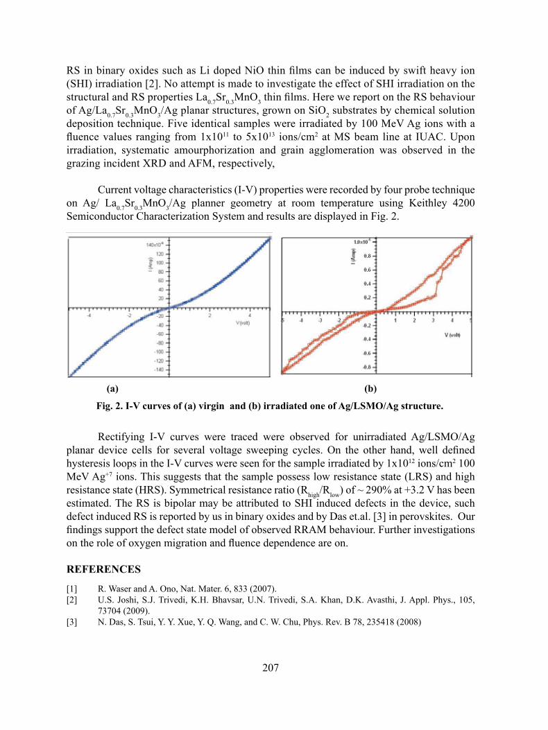
207
RS in binary oxides such as Li doped NiO thin films can be induced by swift heavy ion (SHI) irradiation [2]. No attempt is made to investigate the effect of SHI irradiation on the structural and RS properties La0.7Sr0.3MnO3 thin films. Here we report on the RS behaviour of Ag/La0.7Sr0.3MnO3/Ag planar structures, grown on SiO2 substrates by chemical solution deposition technique. Five identical samples were irradiated by 100 MeV Ag ions with a fluence values ranging from 1x10¹¹ to 5x10¹³ ions/cm2 at MS beam line at IUAC. Upon irradiation, systematic amourphorization and grain agglomeration was observed in the grazing incident XRD and AFM, respectively,
Current voltage characteristics (I-V) properties were recorded by four probe technique on Ag/ La0.7Sr0.3MnO3/Ag planner geometry at room temperature using Keithley 4200 Semiconductor Characterization System and results are displayed in Fig. 2.
(a) (b)
Fig.2.I-Vcurvesof(a)virginand(b)irradiatedoneofAg/LSMO/Agstructure.
Rectifying I-V curves were traced were observed for unirradiated Ag/LSMO/Ag planar device cells for several voltage sweeping cycles. On the other hand, well defined hysteresis loops in the I-V curves were seen for the sample irradiated by 1x10¹² ions/cm2 100 MeV Ag+7 ions. This suggests that the sample possess low resistance state (LRS) and high resistance state (HRS). Symmetrical resistance ratio (Rhigh/Rlow) of ~ 290% at +3.2 V has been estimated. The RS is bipolar may be attributed to SHI induced defects in the device, such defect induced RS is reported by us in binary oxides and by Das et.al. [3] in perovskites. Our findings support the defect state model of observed RRAM behaviour. Further investigations on the role of oxygen migration and fluence dependence are on.
reFerences
[1] R. Waser and A. Ono, Nat. Mater. 6, 833 (2007).[2] U.S. Joshi, S.J. Trivedi, K.H. Bhavsar, U.N. Trivedi, S.A. Khan, D.K. Avasthi, J. Appl. Phys., 105,
73704 (2009).[3] N. Das, S. Tsui, Y. Y. Xue, Y. Q. Wang, and C. W. Chu, Phys. Rev. B 78, 235418 (2008)

208
5.2.39EffectofswiftheavyLi4+ionirradiationonthespraydepositedmolybdenumdopedindiumoxidethinfilms
S. Parthiban1, V. Gokulakrishnan1, K. Ramamurthi1, D. Kanjilal2, K. Asokan2 and I. Sulania2
1Crystal Growth and Thin Film Laboratory, School of Physics, Bharathidasan University, Tiruchirappalli
2Inter-University Accelerator Centre, Aruna Asaf Ali Marg, New Delhi
High visible to near infrared transparent and high carrier mobility 0.5 at. % Mo doped indium oxide (IMO) thin films prepared by spray pyrolysis technique [1]. The details of film preparation and characterization techniques can be found elsewhere [1]. In the present investigation, the as-deposited IMO films were irradiated by 50 MeV swift heavy Li4+ ions with different ion fluencies of 1 × 10¹¹, 1 × 10¹² and 1 × 10¹³ ions/cm2.
XRD studies on the as-deposited and irradiated IMO films confirmed the cubic bixbyite structure of the polycrystalline In2O3 (IO) [2] and the diffraction peaks were identified by matching with the standard data. The obtained diffraction peaks substantiate the polycrystalline structure of the irradiated IMO films. Further, all the irradiated films show a hump between 23.0-28.0° diffraction angle (2θ) that is suggesting the occurrence of amorphization process in the irradiated IMO samples. Additionally, new peaks were obtained at 2θ of ~23.7°, 26.7° and 27.8° which are matched with the standard data and indentified due to the formation of molybdenum oxide (MoO3) phase [3].
The electrical properties are estimated from the room-temperature Hall measurements in van der Pauw configuration. The negative sign of the Hall co-efficient confirmed the n-type conductivity. The as-deposited IMO films (0.5 at. % Mo) reported [1] the best possible combination of electrical properties as follows: resistivity (ρ) of ~5.3 × 10⁻⁴ Ω-cm, µ of ~122.4 cm2/V⋅s and n of ~9.5 × 1019 cm-3. The lowest ρ is observed for 1× 10¹² ions/cm2 ion fluency irradiated IMO thin films. On the other hand, the µ of the irradiated films is decreased from ~122.4 cm2/V.s to ~ 93.3 cm2/V.s for 1 × 10¹² ions/cm2 ion fluency. The transmittance spectra of the irradiated IMO thin films recorded in the wavelength range of 300-2500 nm as a function of Li4+ ion fluencies, along with the spectra obtained from the bare substrate and as-deposited film. The average visible transmittance calculated in the wavelength ranging 500-800 nm is ~77 % for the as- deposited IMO films which decreases to 66.0, 54.5, and 65.4 % for 1 × 10¹¹, 1 × 10¹² and 1 × 10¹³ ions/cm2 ion fluencies, irradiation respectively. The irradiated IMO films show significant decrease in the transmittance characteristics. The atomic force microscope study reveals smoothed surface for 1 × 10¹³ ion/cm2 irradiated films [4].

209
reFerences
[1] S. Parthiban, E. Elangovan, K. Ramamurthi, R. Martins & E. Fortunato, J. Appl. Phys, 106 (2009) 063716.
[2] Powder Diffraction File, JCPDS-International Centre for Diffraction Data-ICDD, Philadelphia, PA Card 06-0416 (1997).
[3] Powder Diffraction File, JCPDS-International Centre for Diffraction Data-ICDD, Philadelphia, PA Card 05-0508 (1997)
[4] S. Parthiban, E. Elangovan, K. Ramamurthi, D. Kanjilal, K. Asokan, D. K. Avasthi, I. Sulania, R. Martins, E. Fortunato, (submitted to journal)
5.2.40Studyofswiftheavyionirradiationeffectonindiumtinoxidecoatedelectrodeforthedye-sensitizedsolarcellapplication
H. K. Singh1, 2, D. C. Agarwal2, P. M. Chavhan3, R. M. Mehra4, Shruti Aggarwal1, Pawan Kumar Kulriya2, Ambuj Tripathi2 and D. K. Avasthi2
1University School of Basic and Applied Science, GGSIPU Delhi 2Inter University Accelerator Center, Post Box-10502, New Delhi 3Thin film Division, National Physical Laboratory, New Delhi 4Department of Electronic Science, University of Delhi, New Delhi
Thin films of ITO are known as a transparent electrode and are now widely used in electronics or optoelectronics including flat panel displays and solar cells [1]. Our main objective is to study the effect of SHI irradiation on photoanode of DSSC to investigate the possibility of improvement in efficiency of DSSC due to ion induced effects in oxide layer and stability of DSSC component in space irradiations. The present work is carried out in light of above background to study the effect of heavy ion irradiation on RF sputtered ITO films. The pristine and irradiated films were characterized using XRD, UV-Vis and Four Probe methods.
The RF sputtered ITO film were procured from Vin Karola Instrument Pvt. Ltd USA. Thickness of film samples was estimated from transmission data [2], and a typical value was ~ 160 nm. These films were irradiated by with 110 MeV, Ni8+ ions at fluences 3x10¹¹, 1x10¹², 3x10¹², 1x10¹³, 3x10¹³ and 1x10¹⁴ ions/cm2.
Fig. (1a) shows the XRD patterns of pristine and SHI irradiated ITO thin films with variable fluence. As compared to pristine ITO films, it is observed that first all peaks were shifted to higher diffraction angle at 3.0x10¹² ion/cm2 fluence, and again come towards their original position as fluence approaches to higher values upto 1.0x10¹⁴ ion/cm2.Therefore it is clear that at low fluences upto 3.0x10¹² ion/cm2, there is strain and beyond 3.0x10¹² ion/cm2 strain is relaxed [Fig. (1b)]. Crystallite size (CS) calculation is helpful for the conductive behavior of the sample. Overall, D is increasing 5nm ( 25nm to 30 nm ), but

210
such little increment has marginal effect in decreasing the band gap of material. Optical transmittance of both irradiated and pristine samples in the wavelength range 350-1000 nm was studied. It is observed that transmittance is the highest at the lowest fluence (3 x 10¹¹ions/cm2) in comparison to pristine sample. This study provides a positive possibility in the context of DSSC application.
Electrical properties of pristine and Ni8+ ion irradiated samples were studied using four probes method. In this measurement, resitivity and sheet resistance is directly measured by four probes. It is observed that resistivity and sheet resistance both increases continuously with increasing fluence (Fig.3). The lowest resistivity and sheet resistance is obtained for pristine sample. Increase in resistivity and sheet resistance may be due to strain, deformation in surface morphology and due to various defects created by ion irradiation. Since strain in the film is increasing upto 3x10¹² ion/cm2 and hence band gap is increasing upto this fluence. Due to increase in band gap upto this fluence, resistivity and sheet resistance of the film increase. But beyond this fluence relaxation occurs in the film and hence band gap will decrease. Still resistivity and sheet resistance of the film are increasing linearly but not with a steep slope. Resistivity will increase if oxygen vacancy decreases. Oxygen vacancies are responsible for conduction in ITO film [3]. There are some reports of depletion of oxygen from the oxides film during high energy ion irradiation [4]. In present study, increase in resistivity with fluence ruled out the possibility of formation of oxygen vacancies under the ion irradiation. There is also release of strain at higher fluences in ITO film. These observations suggest that stress/strain and band gaps of the film are not sole responsible for increasing the resistivity and sheet resistance of the film. It might be due to strain, deformation in surface structure and disorder in lattice and other unfavorable defects along with increase in oxygen content of the ITO film.
Fig.1a.XRD-DiffractogramforITOthinfilmsampleat6differentfluences
Fig.1b.PeakshiftingpatternforITOsampleafterirradiationforplane(222)

211
The aim of present study was to obtain the results of the SHI irradiation on ITO sample (synthesized by RF sputtering) in the context of DSSC application. In this regard, transmittance and resistivity (opposite of conductivity) are the main parameters of ITO sample which decides the efficiency of DSSC. Therefore pristine and irradiated films were characterized in terms of structural, optical and electrical properties. XRD of Pristine and irradiated films were polycrystalline in structure. The transmittance was seen to be increased 13 % compared to pristine sample which is very favorable result from the application point of view of DSSC. The resistivity was found to increase moderately with increase in fluence [2]. The degradation in the electrical properties is marginal with improvement in optical properties, the irradiated films can be used for DSSC application. The difference in behavior of ITO film prepared by RF- sputtering and SP method prepared film [4] under SHI irradiation is due to the initial difference in the micro-structure. The data is being further critically examined in order to understand the mechanism of increase in resistivity.
The RF-sputtered film of ITO is better in terms of radiation resistant behavior and therefore it is useful for space application.
reFerences
[1] SA Knickerbocker , AK Kulkarni ; J Vac Sci Technol A; 13(3) (1995),1048[2] OS Heavens .In: Hass G, RE Thun, editors. Physics of thin films. New York; Academic Press; 1964.
p.203.[3] S-I Jun , TE Mcknight , ML Simpson , PD Rack ; Thin Solid Films;476(2005),59.[4] NG Deshpande et.al.; Vacuum;82(2008),39[5] D.K. Avasthi, W. Assmann, A.Tripathi, S.K. Srivastwa, S.Ghose , F.Gruneer and M. Toulemonde: Phy.
Rev. B 68 , (2003), 153106.[6] D.K. Avasthi, W. Assmann, H. Nolte, H.D. Mieskes, S. Ghose, N.C. Mishra, Nucl. Intrum. Methods
Phys. Res. B 166-167, ( 2000), 345[7] V.V. Ison , A.Ranga Rao , V.Dutta , P.K. Kulriya, D.K. Avasthi and S.K. Tripathi; J.Appl.Phys. 106,
( 2009), 023508.
5.2.41Effectofheavyionirradiationoncorrosion/oxidationbehaviourofamorphousalloys
Shubhra Mathur1, Rishi Vyas1, K. Sachdev1, S. K. Sharma1, Pravin Kumar2 and K. Asokan2
1Department of Physics, Malaviya National Institute of Technology, Jaipur 2Inter-University Accelerator Centre, Aruna Asaf Ali Marg, New Delhi
Metallic glasses are amorphous materials with disorderd structure. The effect of irradiation using both high [1-3] and low energy ion beam [4] in metallic glasses have been of considerable interest from the point of view of surface modification for property enhancement. The specimens of the Ti60Ni40, Ni78Si8B14 and Fe40Ni40B20 metallic glasses were irradiated with Ni11+ 150 MeV ions at a fluence of 1 x 10¹² ions/cm2 and 1 x 10¹³ ions/cm2 delivered by 15 UD Pelletron accelerator at Inter-University Accelerator Centre (IUAC), New Delhi. The aim of the present study is to investigate the change in the thermo-chemical properties of metallic
212
glasses and the phase transformations such as amorphous to crystalline or amorphous to nanocrystalline phase.
The X-ray diffraction (XRD) pattern of the irradiated and unirradiated specimens of the alloy Ti60Ni40 is shown in Fig.1. It is observed that the unirradiated specimen is amorphous in nature whereas in the case of irradiated specimen a nanocrystalline Ti2Ni phase is observed. Potentiodynamic polarization studies were carried out on the unirradiated and irradiated specimen with Ni11+ 150 MeV ions at a fluence of 1 x 10¹³ ions/cm2 of the alloy Ti60Ni40 in 1 M HNO3 aqueous medium and is shown in Fig. 2. The presence of the nanocrystalline phase (Ti2Ni) seems to improve the corrosion resistance of the alloy Ti60Ni40 after irradiation. Potentiodynamic polarization studies were also carried out on unirradiated and irradiated specimens of the alloys Ni78Si8B14 and Fe40Ni40B20 and it is observed that corrosion resistance was better for irradiated specimen.
Fig.1.X-raydiffractionpatterns. Fig.2.Potentiodynamicpolarizationplots
In addition, the low energy 150 KeV N+ ions at a fluence of 1 x 10¹⁵ ions/cm2 and 1 x 10¹⁶ ions/cm2 were used for irradiating the specimens of the Ti60Ni40 amorphous alloy The corrosion behaviour of the irradiated specimen of Ti60Ni40 with 150 KeV N+ ions at a fluence of 1 x 10¹⁶ ions/cm2 was studied using potentiodynamic polarization method in 1 M HNO3 aqueous medium. The partial data analysis was shown that the irradiated specimen exhibits superior corrosion resistance as compared to the unirradiated specimen of the alloy Ti60Ni40.
reFerences
[1] K. V. Amurte, D. C. Kothari & D. Kanjilal, Hyperfine Interact 184 (2008) 185[2] R. Jain, D. Bhandari, N. S. Saxena, S. K. Sharma & A. Tripathi, Bull. Mater. Sci. 24 (2001) 27[3] Jesse Carter, E.G. Fu, Michael Martin, Guoqiang Xie, X. Zhang, Y.Q. Wang, D., Wijesundera, X.M.
Wang, Wei-Kan Chu, Sean M. McDeavitt & Lin Sha, Nuclear Instruments and Methods in Physics Research Section B: Beam Interactions with Materials and Atoms 267 (2009) 2827
[4] S. Nagata, M. Sasase, K. Takahiro, B. Tsuchiya, A. Inoue, S. Yamamoto & T. Shikama, Nuclear Instruments and Methods in Physics Research B 267 (2009) 1514

213
5.2.42GasSensingStudiesofSwiftHeavyIonIrradiatedHydroxyapatiteThickFilms
R. U Mene1, M P Mahabole1, R. P.Sharma2, D. K.Avasthi3, R. S. Khairnar1
1School of Physical Sciences, S.R.T.M.University, Nanded 2Department of Physics, Dr. B.A.M.University, Aurangabad 3Inter University Accelerator Center, Aruna Asaf Ali Marg, New Delhi
Hydroxyapatite [HAp, Ca10(PO4)6(OH)2], is used in various fields such as bio-implant[1], catalyst [2], ion exchanger [3], fuel cell [4], protein separation [5] and chemical gas sensor [6,7]. HAp nano ceramic powder was synthesized by wet chemical process and the thick films were prepared by screen printing technique. These films were irradiated with Ag+7 ions with energy 100 MeV at different fluences ranging from 3x 10¹⁰ to 3x 10¹³ ions/cm2. X-ray diffraction and atomic force microscopy tools were employed to examine the phase & surface modification in HAp thick films due to swift heavy ion irradiation.
Figure (1) shows XRD profiles of pristine & irradiated HAp films as a function of ion fluence. The presence of HAp characteristic peaks reveal the hexagonal phase of the films with crystalline structure up-to a fluence of 3x 10¹¹ions/cm2. The intensities of all XRD peaks are found to be decreasing with increase in fluence.
Figure 2 (A-B) shows the surface topography of the pristine and irradiated HAp thick films by means of atomic force microscopy. The presence of grains can be visualized from the images of pristine HAp films. The grains seem to agglomerate after irradiation and shows more pronounced features of clusters as depicted by Figure 2 (B). It might be due to coalescence effect upon irradiation and is in good agreement with XRD results.
A systematic study of gas sensing was carried out for gases like CO & CO2 using HAp thick film as a sensor. The study concludes that SHI irradiated HAp thick films show the
Fig.1.XRDofHApthickfilmasafunctionofionfluence

214
enhancement in gas sensitivity with ion fluence (Figure 3)and can be used as CO & CO2 gas sensor at an operating temperature 195°C & 165°C respectively.
(A) (B)Fig.2.AFMImageofHApfilm(A)Pristine(B)ionirradiated(3x10¹³ions/cm2)
Fig.3.Changeinsensitivityasafunctionoffluence(A)COgas(B)CO2 gas.
reFerences
[1] Hong Jae Lee, Sung Eun Kim, Hyung Woo Choi, Chan Woo Kim, Kyung Ja Kim, Sang Cheon Lee. Eur. Polymer. J. 43 (2007) 1602.
[2] Kiyotomi Kaneda, Kohsuke Mori, Takayoshi Hara, Tomoo Mizugaki, Kohki. Catalysis Surveys from Asia. (2004) 8.
[3] L. Medvecky, R Stulajtrova, L. Parilak, J. Trpcevska, JDurisin, S.M.Barinov, Collids and surfaces A, 281 (2006) 221.
[4] Young-Sun Park, Yohtaro Yamazaki. Polymer. Bull. 53 (2005) 181.[5] Toru Kanno, Toru Sendai, Kiyoshi Tada, Jun-ichi Horiuchi, Toshiyuki Akazawa. Phosphor. Res. Bull.
21 (2007) 25.[6] M P Mahabole, R C Aiyer, C V Ramakrishna, B Sreedhar, R S Khairnar. Bull. Mater. Sci. 28(6) (2005)
535.[7] R. S. Khairnar, R.U. Mene, M. P. Mahabole, Proceedings of 2nd International Conference on Advanced
Nanomaterials (ANM 2008), University of Aveiro, Portugal, June 22-25, 2008.

215
5.2.43Structure,Microstructureanddielectricpropertiesof107ag15+ and 16O7+ irradiated Ba[(Mg0.32co0.02)Nb0.66]O3thinfilms
Bhagwati Bishnoi1, P.K.Mehta1 and Ravi Kumar2
1Physics Department, Faculty of Science, The M.S.University of Baroda, Vadodara 2Inter University Accelerator Centre, Aruna Asaf Ali Marg, New Delhi
Dielectric/ferroelectric materials have received great attention due to high dielectric constant, low losses and low temperature coefficient of frequency (TCF) and constant (TCK). Majority of the previous work on Ba(B’1/3Nb2/3)O3 have been carried out on bulk materials[1-2]. Thin films of dielectric/ferroelectric have found incredible importance in electronic industries, NVFeram’s, memory devices etc. It has also been observed that in thin films the properties vary considerably compared to bulk. The thin films of Barium, Strontium, Calcium and Bismuth based layered perovskites shows enhancing properties compared to bulk [3-5]. Further, SHI irradiation is known to generate the controlled defects, structural disorder, and modify the strain in the materials.
Single Phase Ba[(Mg0.32Co0.02) Nb0.66]O3 BMCN, targets were prepared using standard solid state reaction technique. BMCN films of 200nm-thick were prepared by Pulsed Laser Deposition (PLD) technique [5]. The Structural analysis of the thin film is
Fig.1.X-raydiffractionpatternofBMCNbulk,Si,MgOandITOcoatedonglasssubstrates.

216
carried out by 3KW X-ray generator with Cu target θ-2θ Goniometer. The well characterized film was irradiated at room temperature with 200 MeV 107Ag15+ and 100MeV 16O7+ ions at fluence of 1x10¹¹, 1x10¹², 1x10¹³ ions/cm2. The beam current was kept around 0.5-1pnA for 107Ag15+ and 16O7+, to avoid heating. The ion beam was focused to a spot of ~1mm diameter and scanned over the entire area of the thin film using a magnetic scanner. The thin film morphology on a wide range of scan lengths (500μm to 1μm) was investigated by atomic force microscopy (AFM) using Nan scope-E from Digital Instruments, USA. Dielectric constant measurement were measured using a Agilent 4285A (LCR) bridge which has a frequency range of 75Khz to 30MHz and operated in the temperature range 100K to 450K.
Fig 1 shows the XRD pattern of BMCN films deposited on different substrates along with the bulk. No impurity phase is detected in the films. It confirms the single phase nature of the films and matches well with the bulk targets. The AFM images of the BMCN films on different substrates were recorded. We observed uniform near Nano size columnar grain formation on Si, Pt-Si and ITO films, while on MgO, we do not notice any grains formation. Average tip size on each substrates are found to be ~100nm (Pt-Si), 20-25nm in Si and 50-60nm in case of ITO coated on glass substrate films. Analysis of growth characteristics from AFM and XRD measurement reveal that films grown on ITO are the better substitute compared to Si, MgO or Pt-Si for electrical properties studies and device application. It allows us to grow films with near nano size columnar grains having potential to enhance dielectric properties, considerably.
Fig.2.Temperaturedependenceofdielectricconstant(a)andtanδ(b)ofBMCNsampleinrange100K-350Kat300KHzforunirradiated,andAg15+ and O7+irradiatedfilms.
Fig. 2 shows the dielectric parameters of samples irradiated at highest fluence. We observe linear temperature dependence of dielectric constant for unirradiated and irradiated
217
samples. The unirradiated film shows abrupt rise in the magnitude of dielectric constant compared to that of bulk, which on correlating with our XRD results indicate that the drastic rise in dielectric constant in the film was mainly due to strain rather than lattice mis-match, as there is marginal increase in the value of lattice constant of film compared to bulk. There is a drastic fall in values on irradiation, dictated by the type of defects created in the films along the latent tracks. We observe nearly temperature independent dielectric loss for unirradiated and 107Ag15+ irradiated films while for 16O7+ irradiated film it shows drastic rise. 107Ag15+ ion irradiation reduces the dielectric loss to the order of 10-3.
reFerences
[1] Surya M. Gupta E. Furman, E. Colla, and Z. Xu Dwight Viehland J App Phys 88, (2000) 2836 [2] Cheol-Woo Ahn, Hyun-Jung Jang, Sahn Nahm, Hyun-Min Park, Hwack-Joo Lee J European Ceram
Soc. 23, (2003) 2473.[3] J. Petzelt, T Ostachupk J Optoelectronics and Advanced Materials 5, (2003) 725.[4] L.S. Cavalcante, A.Z. Simões, L.P.S. Santos, M.R.M.C. Santos, E. Longo and J.A. Varela J Solid State
Chemistry 179 (2006) 3739.[5] P.K.Mehta, Bhagwati Bishnoi, Ravi Kumar, R.J.Choudhary and D. M. Phase Solid State Phenomena
155 (2009) 145.
5.2.44 86 MeV O6+ionirradiatedmodificationsinPVDC
Sonika Thakur1, Kawaljeet Singh Samra1and Lakhwant Singh1
1Department of Physics, Guru Nanak Dev University, Amritsar
Heavy ion irradiation of polymers results in many physical and chemical changes, e.g., density, conductivity [1], molecular weight distribution and solubility which cannot be achieved in a routine synthetic way. These changes depend on ion parameters (energy, mass and fluence). The primary phenomena associated with ion-polymer interaction are cross linking, chain scission and emission of atoms, molecules and molecular fragments.
In the present work, the modification brought about in PVDC by swift heavy ions is reported in terms of optical, chemical and structural changes. PVDC is chosen for present study since it possesses simple linear chain chemical structure that helped to keep the number of variables in the study as low as possible. Thin films of PVDC have been irradiated with O6+
ion beam having energy of 86 MeV using 15 UD pelletron at IUAC New Delhi. Irradiation has been made at four different fluences from 3.2x10¹¹ to 1x10¹³ ions/cm2. The changes in the value of optical band gap and the number of carbon atoms per cluster have been calculated from the UV-VIS analysis of the pristine and SHI treated polymer. With increasing fluence, the decrease in the band gap energy and increase in the cluster size have been observed. All the absorption spectra of irradiated PVDC show bathochromic shift as well as hyperchromic effect with the increase of ion fluence. One of the possibilities behind this behavior is interpreted as the formation of extended system of conjugated bonds i.e. carbon clusters in

218
PVDC due to irradiation. It is found that the formation of these carbon enriched zones during irradiation of polymer is responsible for the observed colour change of the irradiated polymer samples. Darkening of the irradiated films at higher fluences and in the deeper layers has been attributed to beam induced carbonization and we suspect that this results in the formation of chromophores, which are light-absorbing groups of conjugated polymers [2]. Evidence of this is shown in the FTIR which results in the double peak formation at 1780 cm-1. The increase in the absorption bands in the 1640 cm-1 and the 1780 cm-1 regions, due to irradiation, has been attributed to the creation of unsaturated -C=C- bonds for the first one and a beginning of polymer oxidation for the second [3]. It is observed from the XRD measurements that in Oxygen ion irradiated PVDC there is a decrease in the crystallanity with the increase of ion fluence, which may be attributed to radiation induced chain scission [4].
reFerences
[1] D. Fink, K. Ibel, P. Goppelt, J.P. Biersack, L. Wang and M. Behar, Nucl. Instr. And Meth. B 46 (1990) 342.
[2] T. W. G. Solomon, Organic Chemistry, Wiley 5th ed., 1992.[3] J. Davenas, and X. L. Xu, Nucl. Instr. and Meth. B 39 (1989) 754. [4] L. Singh, K.S. Samra, Journal of Macromolecular Science, Part B : Physics, 46: 1041-1049, 2007
5.2.45Swiftheavyionirradiationinducedbenzenoidtoquinoidtransitioninpolyanilinenanofibers
Somik Banerjee1 and A. Kumar1
1Materials Research Laboratory, Dept. of Physics, Tezpur University, Tezpur, Assam
Swift heavy ion (SHI) irradiation causes exotic effects in different classes of materials which otherwise cannot be generated by any other means. SHI irradiation has already been used as an efficient tool for enhancing the physico-chemical properties of conducting polymers such as conductivity, electrochemical stability, sensing properties etc.1, 2 The primary phenomena associated with the interaction of ion beam and polymers are cross-linking, chain scission and emission of atoms, molecules and molecular fragments.3 However, applicability of the SHI irradiation as a potential tool for tailoring the structure, size and properties of conducting polymer nanostructures has not been fully investigated. In this report we present the micro-Raman studies of 90 MeV O7+ ion irradiation induced structural and conformational changes in camphor sulfonic acid (CSA) doped PAni nanofibers embedded in PVA matrix.
PAni nanofibers were synthesized by interfacial polymerization technique4 using CSA as dopant and subsequently purified and uniformly dispersed in a 2% PVA solution for casting thin films (~50 µm) on glass slides of area 1 cm2 for irradiation purpose. Thin films of the nanofibers were irradiated with 90 MeV O7+ ions at fluence from 3x10¹⁰ to

219
1x10¹² ions/cm2 using the 15UD Pelletron accelerator. The sample was irradiated at normal beam incidence. A Renishaw invia Raman microscope with Ar ion laser (power: 0.5 mW; excitation: 514.5 nm; exposure time: 10 s) was used to acquire the micro-Raman (µR) spectra of the pristine and irradiated samples.
Figure 1 shows the micro-Raman (µR) spectra of the pristine and irradiated PAni nanofibers doped with CSA. In the µR spectra, for pristine polyaniline nanofibers the bands at 1448.15 cm-1 and 1409.00 cm-1 correspond to the C=N stretching mode of the quinoid units. The band at 1245 cm-1 can be assigned to the C–N stretching mode of the polaronic units. The absorption bands at 1325, 1344 and 1375 cm-1 correspond to the C–N•+ stretching modes of the delocalized polaronic charge carrier which indicates that the PAni nanofibers are in doped ES-I form. The absorption peak at 1527 cm-1 corresponds to the N–H bending deformation band of protonated amine. The main peak located 1595 cm-1 originate from the symmetric C=C stretching mode of the benzenoid ring of PAni. The characteristic Raman peaks of polyaniline at 1245, 1325, 1344, 1375, 1527 and 1595 cm-1 decrease in intensity and broaden as the fluence is increased. It is well known that the Raman bands of PAni at wavenumbers higher than 1000 cm-1 are sensitive to its oxidation and protonation state.5 The results imply that the electronic interaction between the electron rich C–N site in the aromatic ring of PAni chains and the ion beam might have induced distortion of the polymeric chains leading to conformational modifications of the PAni nanofibers. It has been observed that with the increase in ion fluence, the intensities of the Raman vibrating modes at 1245, 1325, 1344 and 1375 cm-1 due to the doping states (polaron states) of the PAni nanofibers decreases. The results suggest that the PAni nanofibers are transferred from doped to de-doped states, i.e., reduction states through the ion beam treatment, because of the electronic interactions of the irradiating ion beam, the negative Cl- counterions and the positively charged PAni nanofiber chains.
The most significant change in the micro-Raman spectra of the PAni nanofibers after SHI irradiation is that the symmetric C=C stretching peak at 1595 cm-1 can be deconvoluted into two sub-peaks. The sub-peaks indicate two kinds of resonant structures: the main peak is due to the benzenoid structure and the shoulder peak is due to the quinoid structure of the PAni nanofibers. The main peak of the symmetric C=C stretching mode is up-shifted from 1600.8 to 1602.9 cm-1 [Fig. 2] and the intensity decreases from 1228 to 450.34 upon irradiation. The shoulder peak of the symmetric C=C stretching mode is also up-shifted from 1624.3 to 1632.9 cm-1 [Fig. 2] and intensifies more than 3 times from 97.56 to 353.85 upon irradiation. This suggests that there is a transformation from benzenoid to quinoid structure upon SHI irradiation in the PAni chains which leads to a decrease in the π-conjugation length. The Raman peak broadening may be attributed to the variation in the π-conjugation length of the PAni chains, which is associated with π-electron delocalization.6

220
reFerences
[1] A. M. P. Hussain, A. Kumar, F. Singh and D. K. Avasthi, J. Phys. D: Appl. Phys. 39, 750 (2006).[2] A. Srivastava, V. Singh, C. Dhand, M. Kaur, T. Singh, K. Witte and U. W. Scherer, Sensors 6, 262
(2006).[3] J. Davenas, G. Boiteux, X. L. Xu and E. Adem, Nucl. Instrum. Methods B, 32, 136 (1988).[4] J. Huang, R. B. Kaner, J. Am. Chem. Soc. 126, 851 (2004).[5] M. Tagowska, B. Palys and K. Jackowska, Synth. Met. 142, 223 (2004).[6] E. A. Bazzaoui, G. Levi, S. Aeiyach, J. Aubard, J. P. Marsault, and P. C. Lacaze, J. Phys. Chem. 99,
6628 (1995).
5.2.46Mechanism ofChargeTransport in 100MeVSwiftHeavy Ions (Silver (Ag8+))BeamirradiatedPoly(3-Hexyl-Thiophene)
Amarjeet Kaur1, Anju1 and D.K. Avasthi2
1Department of Physics and Astrophysics, University of Delhi 2Inter University Accelerator Center, Aruna Asaf Ali Marg, New Delhi
Poly (3-hexyl thiophene) films have been prepared by chemical oxidation i.e. Sugimoto method [1]. In order to see the effect of radiation and to explore their possible applications, the fully undoped samples were irradiated with different fluences of 100 MeV silver (Ag8+) ions. Appropriate thickness of all the polymeric films have been selected by Monte-Carlo simulation program SRIM so as to be thin enough to allow the 100MeV ions
Fig.1.Micro-RamanspectraofCSAdopedpolyanilinenanofibers(a)beforeandafterirradiationwith90MeVO7+ionsatfluences(b)3x10¹⁰,(c)3x10¹¹and(d)1x10¹²ions/cm2.

221
to completely pass through it. The temperature dependence of dc and ac conductivity of irradiated as well as unirradiated samples has been investigated in 77-300K in P3HT. In present investigations the effect of 100 MeV Ag8+ ions (at different fluences) on the conductivity of pristine (i.e. fully undoped) poly (3-hexyl thiophene) has been discussed in detail. The temperature dependence of dc conductivity in all the samples has been analyzed in light of Mott’s variable range hopping model [2]. Fig. 1(a) shows variation of dc conductivity as inverse temperature. As thermal energy decreases with temperature, there are fewer nearby states with accessible energies, so the mean range of hopping increases, which leads to the following expression for conductivity
(1)
where β = 1/n+1, where n is the dimensionality, thus β =1/2, 1/3 and 1 /4, respectively for 1D, 2D and 3D hopping transport. T0 and σ0 are constants and are expressed functionally as
(2)
and (3)
where T0 is the characteristic temperature, λ is the dimensionless constant [3,4] and is assumed to be 18.1, α is the coefficient of exponential decay of the localized states involved in hopping process, kB is the Boltzmann’s constant, N(EF) is the density of states at Fermi level, e is the electronic charge, σ0 is the conductivity at infinite temperatures, υ0 is the phonon frequency (˜1013Hz) and can be obtained from Debye’s temperature θD [6] and R is the hopping distance between the two sites. It has been observed that our conductivity data for all the samples pristine (X0), irradiated at 1010ion/cm2 (X1), 1011ion/cm2 (X2) and 1012ion/cm2 (X3) fits best into linear curve for β = 1 /4 and the variation of dc conductivity as a function of T-1/4 has been shown in Figure 1(b). Therefore, 3D VRH seems to be the mechanism of charge transport in all the samples. The other two important parameters the average hopping distance R and the average hopping energy W have also been calculated. The density of states N(EF) lies in the range 1019-1020 cm-3eV-1 which is in good agreement with the values calculated for other polyheterocyclics and other conjugated polymers [5,6]. The values of activation energy along with that of dc conductivity have been calculated by the relation.
EA = (4)
The observed temperature dependence of activation energy rules out band conduction, in unirradiated as well as irradiated samples. Therefore, it supports that hopping conduction (σH) may be the dominant mechanism of charge transport. The plot in the temperature region where Eq. (1) is valid should give activation energy as per Eq. (4) and can be correlated to the parameters of Eq. (1) by the following equation

222
(5)
Fig.1.ThePlotofdcconductivity(σdc)asareciprocalofTemperature(a)1000/Tand (b)T-1/4intherangeof(77-300K)ofPristine(X0)and100MeVAgion irradiatedX1,X2andX3P3HTand(c)LogActivationEnergy(Ea)vslog
temperature(T)ofPristine(X0)andX1.
It is evident from Eq.(5) that a plot of logEA versus log T should yield a straight line of slope –(β-1). The solid corresponding to β=1/4 is shown in Fig. 1(c). It can be seen that the slope of the solid line is almost parallel to obtained log activation energy data versus log T, which as a representative result has been shown for X0 and X1. This further indicates that three dimensional variable range hopping is dominant in both irradiated as well unirradiated samples [6]. Mott’s 3D hopping model successfully explains the mechanism of charge transport in pristine and all the irradiated samples. While increase in conductivity due to fluence of silver ions, it does not overcome it phonon assisted mobile charge carriers.
The charge transport mechanism is not altered due to the irradiation for the range of conductivity in present investigations. However without using dopants, the conductivity increases by two orders till fluence F2. No degradation or decay in conductivity has been observed, even when the samples were kept in atmospheric conditions for more than eight months.

223
reFerences
[1] R. K. Singh, J. Kumar, R. Singh, R. Kant, R. C. Rastogi, S. Chand and V. Kumar, New J. Phys. 8, 112, 5 (2006).
[2] N F Mott and E A Davis 1979 Electronic Processes in Noncrystalline Materials 2nd edn (London: OxfordUniversity Press).
[3] R. Singh and A. K. Narula, J. Appl. Phys. 82, 4362 (1997).[4] D. K. Paul and S. S. Mitra, Phys Rev. Lett. 31, 1000 (1973).[5] R. Singh and A. K. Narula, J. Appl. Phys. 82, 4362 (1997).[6] R. Singh, J. Kumar, A. Kaur, K. L. Yadav, R. Bhattacharya, E. Hussain and S. Ali, Polymer 47 6042
(2006). A. Kaur, A. Dhillon and D. K Avasthi, J. Appl. Phys. 106, 1 (2009).
5.2.47Structural Changes In Makrofol-KgAnd Pet By 120 Mev Ni+9 Ion Beamirradiation
Ambika Negi1, Anju Semwal1, D.Kanjilal2, R.G.Sonkawade2, J.M.S.Rana1and R.C.Ramola1
1Dept. of Physics, HNB Garhwal University, Badshahi Thaul Campus, Tehri Garhwal
2Inter University Accelerator Center, Aruna Asaf Ali Marg, New Delhi
High-energy ion bombardment induced modifications in polymeric materials are quite interesting and involved field of research. The swift heavy ions (SHI) at velocity of the order of Bohr velocity lose their energy mainly via electronic excitation and ionizations. The deposited energy gets converted into atomic motion and finally leads to the structural and chemical modifications with in a cylindrical zone of a few nanometers in diameter [1, 2].
Long chain molecular structure of polymers gives rise to their interesting properties for use in devices and solid-state nuclear track detectors. In the present investigation, an attempt has been made to compare the changes induced in the structural, optical and chemical properties of Makrofol-KG and Polyethylene Terephtalate (PET) due to irradiation by 120 MeV Ni+9 ions. Optical and structural properties are investigated by UV-Visible spectroscopy and X-ray diffraction. The XRD pattern of pristine and Ni+9 ion beam irradiated Makrofol-KG is shown in Fig. 1(a) and XRD of PET is shown in Fig. 1(b). In pristine sample of Makrofol-KG, it is observed that strong peak occurs at 17.36o. It shows that Makrofol-KG is semi crystalline in nature. After irradiation with Ni ions with increasing fluences the intensity of peak decreases sharply. This shows that the polymer crystallinity decreases with increasing fluence and undergoes amorphization. PET shows similar trends under irradiation. Pristine PET shows strong peak at 2θ=25.94 degree and weak peak at 2θ=23.46 degree. After irradiation, peak intensity is found to decreases with increasing fluences but no significant shift of peak position is observed. This implies that

224
the lattice parameter do not change significantly [3]. The UV-Visible spectra were recorded for the pristine and ion irradiated polymers. A shift in absorption edge towards longer wavelength with increasing fluences can be readily observed. It indicates a decrease in band gap after SHI irradiation, which gives rise to the increase in the conductivity of the polymer. This shift in the absorption may be due to creation of free radicals and molecules during irradiation by highly energetic heavy ion.
Fig.1(a)XRDpatternofPristineMakrofol-KGandirradiatedwithNibeam
Fig.1(b)XRDpatternofPristinePETandirradiatedwithNibeam
reFerences
[1] A. Adle, V. Buschmell, H. Fuess & C. Trautmann, Nucl. Instrum. Meth. B185 (2001) 210[2] T. Venkatesan, Nucl. Instrum. Meth. B461 (1985) 7[3] Y. Wang, Y. Jin, Z. Zhu, C. Liu, Y. Sun, Z. Wang, M. Hou, X. Chen, C. Zhang, J. Liu and B. Li, Nucl.
Instrum. Meth. B420 (2000) 164-165
5.2.48ProtonbeamdosimetryusingnanocrystallineK2ca2(SO4)3:Eu
S.P. Lochab1, Shaila Bahl2, A.A. Rupasov3, V E Aleynikov4, A Molokanov4, A. Pandey5
1Inter-University Accelerator Centre, Aruna Asaf Ali Marg, New Delhi 2All India Institute of Medical Science, Ansari Nagar, New Delhi. 3P.N. Lebedev Physical Institute, Russian Academy of Sciences, Moscow, Russia 4Joint Institute for Nuclear Research, Dubna 141980, Russia. 5Department of Physics, Sri Venkateswara College, University of Delhi, Delhi
In the present work the technique of TL dosimetry has been further studied for proton beam using nanocrystalline K2Ca2(SO4)3:Eu. The nanophosphor shows certain characteristics that make it superior in many ways to the other phosphors studied so far. Nanophosphor

225
K2Ca2(SO4)3:Eu of post proton beam irradiation has been studied to study the phosphors suitability as a dosimeter material for accurately measuring the doses of proton beam over a wide range doses. Pellets form of the nanomaterial was irradiated by 150 MeV Proton ion beams at Dubna. Over the dose range of 0.1Gy to 325 Gy the nanophosphor showed a linear increase in TL response.
5.2.49Comparative study of different nanocrystallineTL dosimeters with 150MeVProtonbeam
S.P Lochab1, V.E. Aleynikov2, A Molokanov2, A A Rupasov3, Shaila Bhal4
1Inter-University Accelerator Centre, Aruna Asaf Ali Marg, New Delhi 2Joint Institute for Nuclear Research, Dubna 141980, Russia 3P.N. Lebedev Physical Institute, Russian Academy of Sciences, Moscow, Russia 4AIIMS, Anrasi Nagar, New Delhi.
The newly developed nano-phosphors of BaSO4:Eu, CaSO4:Eu, K2Ca2SO4:Eu and Ba0.97Ca0.03SO4:Eu were exposed with 150 MeV proton beam in JINR, Dubna, Moscow region. The TL results for very high energy of proton ion beam were analyzed. Energy of the beam at the beam entrance at the procedure room is 171 MeV. The beam moderation was performed by means of PMMA energy degraders. Additional energy PMMA moderator equivalent of 40 mm water was placed before the final collimator. Detectors were irradiated in the modified Bragg peak (using Ridge filter) of depth-dose distribution. Dosimetry calibration at the each point of detectors irradiations were performed by means of ionization chamber and clinical dosimeter KD-27012.
Sets of detectors were exposed behind additional degrader equivalent of 150 mm of water at the Spread out Bragg peak (SOBP) for different absorb dose ranging from 0.1Gy to 300Gy. The thermoluminescence (TL) glow curves along with the response curves of these nanophosphors have been investigated. The TL saturation effect is a major problem in case of ion-beams dosimetry and hence it is almost impossible to measure high doses very accurately. The saturation occurs due to the ion-tracks overlapping each other in the material at higher doses. However, with the use of very tiny particles such as nanoscale TLD materials, this problem is overcome to a major extent.
5.2.50ThermoluminescenceresponseofCaS:Bi3+nanophosphorexposedto200MeVag+15ionbeam
Vinay Kumar1, H.C. Swart1, O.M. Ntwaeaborwa1, Ravi Kumar2, S.P. Lochab2, Varun Mishra3, Nafa Singh4
1Dept. of Physics, University of the Free State, Bloemfontein 9300, South Africa

226
2Inter-University Accelerator Centre, Aruna Asaf Ali Marg, New Delhi 3Department of Physics, Lovely Professional University, Phagwara, Punjab 4Department of Physics, Kurukshetra University, Kurukshetra, Haryana
A study of the thermoluminescence (TL) parameters has been performed on swift heavy ion exposed Bi3+ doped CaS nanophosphors prepared by the chemical co-precipitation method. All the samples have been exposed to 200 MeV Ag+15 ions in a fluence range of 1 x 10¹² – 1 x 10¹³ ions/cm2. The prominent TL glow peak at 403 K (observed for the c-irradiated sample) appeared at the same position in the 200 MeV Ag+15 ion beam irradiated samples, while the other peak at 466 K disappeared and the broad peak normally measured at 534 K split into two peaks at 535 K and 582 K for the Ag+15 ion beam irradiated samples. The effect of different Bi3+ concentration has been investigated and it was found that the maximum TL intensity was measured for the 0.08 mol% sample. The effect of different heating rates on the TL response has also been determined. The trapping parameters (i.e. activation energy, frequency factor, order of kinetic) of all the individual peaks of the glow curves have been analysed by using Chen’s formulae. The low fading and linear TL response in the range of 1 x 10¹² – 1 x 10¹³ ions/cm2 will be helpful to explore the potential use of this material for heavy ion dosimetry.
5.2.51LowTemperature resistivity study of nanostructured polypyrrole films underelectronicexcitations.
Subhash Chandra1, S. Annapoorni2, Fouran Singh3, R.G. Sonkawade3, J.M.S. Rana1, R.C. Ramola 1
1Dept. of Physics, HNB Garhwal University, Tehri Garhwal 2Department of Physics and Astrophysics, University of Delhi, Delhi 3Inter University Accelerator Center, Aruna Asaf Ali Marg, New Delhi
The synthesis of nanostructured polypyrrole (Ppy) films by electrochemical process and their modifications by electronic excitations induced by swift heavy ion irradiations is reported in this paper. The electrical property of ion beam irradiated polypyrrole was investigated at low temperature by resistivity measurements. The structural and optical properties were also studied using X-ray diffraction (XRD), UV–vis spectroscopy and scanning electron microscopy (SEM). At low temperature, the polypyrrole films show the metallic behaviour after ion beam irradiation. UV–vis spectroscopy shows a red shift in the absorbance edge and thus reduction in band gap with increasing ion fluence. The structural studies show that the percentage crystallinity improves with increase in ion fluence. The SEM study corroborates the results of structural analysis and shows the formation of rod type structures along with the evolution of amorphous phase with increasing ion fluence.
227
5.2.52Effects of Oxygen Ion Beam (O+7, 100 MeV) and Gamma Irradiation onPolypyrroleFilm
Subhash Chandra1, S. Annapoorni2, Fouran Singh3, R. G. Sonkawade4, J. M. S. Rana1, R. C. Ramola1
1Dept. of Physics, HNB Garhwal University, Tehri Garhwal 2Department of Physics and Astrophysics, University of Delhi, Delhi 3Inter University Accelerator Center, Aruna Asaf Ali Marg, New Delhi
Nanostructured polypyrrole films doped with para-toluene sulfonic acid were prepared by an electrochemical process, and a comparative study of the effects of swift heavy ions and γ-ray irradiation on the structural and optical properties of the polypyrrole was carried out. Oxygen-ion (energy ~ 100 MeV) fluence varied from 1010 to 3 x 10¹² ions/cm2, and the γ dose varied from 6.8 to 67 Gy. The polymer films were characterized by X-ray diffraction, ultraviolet–visible spectroscopy,and scanning electron microscopy. The X-ray diffraction pattern showed that after irradiation, the crystallinity improved with increasing fluence because of an increase in the crystalline regions dispersed in an amorphous phase.
The ultraviolet–visible spectra showed a shift in the absorbance edge toward higher wavelengths, which indicated a significant decrease in the band gap of the polypyrrole film after irradiation. The scanning electron microscopy study showed a systematic change in the surface of the polymer. A similar pattern was observed with the γ irradiation.
5.2.53Studyofopticalbandgap,carbonaceousclustersandstructuringinCR-39andPETpolymersirradiatedby100MeVO7+ions
R.C.Ramola1, Subhash Chandra1, Ambika Negi1, J.M.S.Rana1, S. Annapoorni2, R.G. Sonkawade3, P.K. Kulriya3, A. Srivastava4
1Dept. of Physics, HNB Garhwal University, Tehri Garhwal 2Department of Physics and Astrophysics, University of Delhi, Delhi 3Inter University Accelerator Center, Aruna Asaf Ali Marg, New Delhi 4Department of Chemistry, Punjab University, Chandigarh
Commercially purchased CR-39 and PET polymers were irradiated by 100MeV O7+ ions of varying fluences, ranging from 1011 to 1013 ions/cm2. The effects of swift heavy ions (SHI) on the structural, optical and chemical properties of CR-39 and PET polymers were studied using X-ray diffraction (XRD), UV–visible spectroscopy and Fourier transform infrared (FTIR) spectroscopy. The XRD patterns of CR-39 show that the intensity of the peak decreases with increasing ion fluence, which indicates

228
that the semicrystalline structure of polymer changes to amorphous with increasing fluences. The XRD patterns of PET show a slight increase in the intensity of the peaks, indicating an increase in the crystallinity. The UV–visible spectra show the shift in the absorbance edge towards the higher wavelength, indicating the change in band gap. Band gap in PET and CR-39 found to be decrease from 3.87 to 2.91 and 5.3–3.5 eV, respectively. The cluster size also shows a variation in the carbon atoms per cluster that varies from 42 to 96 in CR-39 and from 78 to 139 in PET. The FTIR spectra show an overall reduction in intensity of the typical bands, indicating the degradation of polymers after irradiation.
5.2.54Swiftheavyionsinducedmodificationsinstructuralandelectricalpropertiesofpolyaniline
R.C.Ramola1, Subhash Chandra1, J.M.S.Rana1, Raksha Sharma2, S. Annapoorni 2, R. G. Sonkawade3, and Fouran Singh3
1Dept. of Physics, HNB Garhwal University, Tehri Garhwal 2Department of Physics and Astrophysics, University of Delhi, Delhi 3Inter University Accelerator Centre, Aruna Asaf Ali Marg,New Delhi
The ion fluences range from 5 × 10 10 to 1 × 10 12 ions/cm 2 irradiation effects of 50 MeV Li 3+ and 90 MeV C 6+ ion beams on free-standing polyaniline (PANI) films have been investigated. The X-ray diffraction study shows an increase in crystalline nature of the PANI film with increasing fluence, followed by a decrease beyond the critical ion fluence. I–V characteristics reveal increased conductivity in the irradiated films. Scanning electron microscopy shows the formation of clusters and craters at higher fluences.