56 - digital library/67531/metadc696163/m2/1/high... · 56 approved for public ... (eovt) and...
TRANSCRIPT

5 6 Approved for public release; disfribufion is unlimited.
Title:
Author@):
Submitted to
Los Alarnos N A T I O N A L L A B O R A T O R Y
MANUFACTURING CHALLENGES OF OPTICAL CURRENT AND VOLTAGE SENSORS FOR UTILITY APPLICATIONS
ECEIVED
M. A. BRUBAKER, C. P. YAKYMYSHYN, P. M. JOHNSTON, AND C . REINBOLD,
SPIE CONFERENCE ON INTELLIGENT SYSTEMS AND ADVANCED MANUFACTURING
Los Alamos National Laboratory, an affirmative action/equal opportunity employer, is operated by the University of California for the U.S. Department of Energy under contract W-7405-ENG-36. By acceptance of this article, the publisher recognizes that the U.S. Government retains a nonexclusive, royalty-free license to publish or reproduce the published form of this contribution, or to allow others to do so, for US. Government purposes. Los Alamos National Laboratory requests that the publisher identify this article as work performed under the auspices of the US. Department of Energy. The Los Alamos National Laboratory strongly supports academic freedom and a researcher's right to publish: as an institution. however, the Laboratory does not endorse the viewpoint of a publication or guarantee its technical correctness. I Form 836 (10/96)
DISCLAIMER
This report was prepared as an account of work sponsored by an agency of the United States Government. Neither the United States Government nor any agency thereof, nor any of their employees, makes any warranty, express or implied, or assumes any legal liability or responsibility for the accuracy, completeness, or use- fulnw of any information, apparatus, product, or process disclosed, or represents that its use would not infringe privately owned rights. Reference herein to any spe- cific commercial product, process, or service by trade name, trademark, manufac- turer, or otherwise dots not necessarily constitute or imply its endorsement, recorn- mendktion. or favoring by the United States Government or any agency thereof. The views and opinions of authors expressed herein do not necessarily state or reflect those of the United States Government or any agency thereof.

Manufacturing challenges of optical current and voltage sensors for utility applications
(Invited Paper)
Christopher P. Yakymyshyna , Michael A. Brubakerb, Paul M. JohnstonC and Chns Reinboldd
a Dept. of Electrical and Computer Engineering, Montana State University, Bozeman, MT bLos Alamos National Laboratory, Los Alamos, NM
CConsultant, Raleigh, NC dABB High Voltage Switchgear, Greensburg, PA
ABSTRACT
Nonconventional instrument transformers based on intensity modulation of optical signals have been reported in the literature for more than 20 years. Recently described devices using passive bulk optical sensor elements include the Electro- Optic Voltage Transducer (EOVT) and Magneto-optic Current Transducer (MOCT). These technologies offer substantial advantages over conventional instrument transformers in accuracy, optical isolation, bandwidth, environmental compatibility, weight and size. This paper describes design and manufacturing issues associated with the EOVT a6d the Optical Metering Unit ( O w recently introduced by ABB with field installation results presented for prototype units in the 345 kV and 420 kV voltage classes. The OMU incorporates an EOVT and MOCT to monitor the voltage and current on power transmission lines using a single free-standing device.
Keywords: Optical sensors, voltage, current, pockels, faraday.
1. INTRODUCTION
Measurement of voltages and currents in power transmission and distribution systems are critical to the electic utllity industry for both revenue metering and reliability. Nonconventional optical methods for making such measurements have been reported in the literature for many years. Recent advances using passive bulk optical sensors include the electro-optic voltage transducer (EOVT) and magneto-optic current transducer ( M O O which may be combined into a single optical metering unit (OW). These new sensors provide substantial advantages in accuracy, galvanic isolation, bandwidth, sue, weight and environmental compatibility. Furthermore, such optical sensors eliminate feno-resonance effects and can be used either as free-standing devices or incorporated into other components of the power system.
%le such sensor concepts have been understood for some time, the challenge has remained to transition optical sensors from the laboratory into hardened commercial devices which meet stringent utility standards. This paper documents design and manufacturing issues associated with the optical metering unit (OMU) recently introduced by ABB and a discussion of utility industry applications is provided to better emphasize the importance of this technology. The critical aspects of the O W include opticd design, dielectric and mechanical packaging, type testing, electronicdinterfacing and calibration. This product utilizes standard components to cover a range of voltage classes and thus becomes cost competitive with conventional oil-filled, wound magnetic core based technologies. Testing and field installation results are presented for selected systems and various practical issues including calibration, operations and maintenance are discussed.
2. OVERVIEW OF APPLICATIONS
Measurements of voltage and current are fundamental to revenue metering and control of the electric power system. Since the latter half of the 19th century, this function has been carried out primarily by wound iron-core transformers specifically designed to measure these variables. The accuracy, stability, and reliability of these devices have been excellent and one should expect that they will used into the future. However, today there are factors associated with the dynamic environment

of the electric utility industry that are beginning to pressure these well-proven designs. This changing environment has accelerated the development of non-conventional sensors for electric utility applications.
Unconventional sensors are not new. For decades, there have been designs brought to production that address one or more of the perceived disadvantages of transformers. Among these are capacitor dividers for reduction of voltage levels, the elimination of iron cores in current sensors to increase operating raage and linearity, and even the application of electronics. In most cases, non-conventional measurement schemes have been addressing the relatively high cost or quality control issues of iron core designs. These new approaches have tended toward the higher voltage applications where conventional transformer costs begin to increase at an exponential rate. In most cases, these alternative designs involve some compromise to the accuracy or stability of conventional transformers; but there are applications where they are a cost-effective and acceptable approach.
Optical techniques have been looked at for some time as method for making these measurements on power transmission systems, especially at high voltage. The complete dielectric isolation offered by an optical system is considered to be one of the primary benefits. This factor becomes increasingly important as measurement and control equipment for the power system becomes more electronic in nature. For these systems, the ability of optical sensors to “disconnect” the electronics from the hazards presented by the power system in the form of voltage transients is a major factor in increasing reliability. A related benefit of galvanic isolation is the lack of interaction between the sensor and the measured parameter. Issues such as ferro-resonant conditions, caused by the interaction of iron core devices and capacitance, are non-existent with totally optically-based designs.
For most optical designs, the equipment that results is significantly smaller and lighter than could be achieved with conventional insulation systems. When this fact is taken advantage of, the equipment requires less space in the substation and the amount of labor and equipment needed for installation is reduced. In the new economic environment brought on by deregulation, the effect is to lower the total costs of ownership which clearly makes optical sensors more amctive and offsets the higher initial costs of these devices. Additional savings are realized in terms of environmental compatibility since the optical sensor structures can be gas-insulated. l h s eliminates the use of mineral oil typically required in conventional devices which has become a significant liability for many utilities in recent years.
In the substation, the most common measurement device is for cunent. Optical sensor elements, by virtue of their small size and weight, can be integrated into existing substation equipment such as circuit breakers and switches. This has the obvious advantage of eliminating the need for a separate insulation and weather protection envelope for the optical path which can be a large percentage of the unit cost. Furthermore, there is an additional advantage in that control devices like circuit breakers can be operated more effectively with the information provided by a larger number of closely coupled sensors. The development of optical sensors will thus augment existing efforts to automate power system control and operation.
From a manufacturing viewpoint, the use of optics opens the possibilities of dramatic cost reductions in the fabrication of high voltage measurement equipment. While the cost of materials is generally higher than with conventional transformers, this can be offset by the reduction of labor content and capital equipment which optical sensors offer. In general, well- designed optical sensors can be mass-produced without the constraint of knowing the final application voltage or current. This offers a significant advantage in reduction of manufacturing cycle time and inventory requirements, particularly when combined with standardized designs which use common parts over a wide range of applications.
In one form or another, the advantages of optical sensors have led instrument transformer manufacturers to develop and begin field application trials of these devices. In the remainder of this paper, the operating principles of intensity modulated voltage and current sensors will be discussed, leading to a description of commercial products based on these principles. Current sensing is accomplished with a Magneto-Optic Current Transducer ( M O W and voltage measurements are made with an Electo-Optic Voltage Transducer (EOVT). A complete power measurement device is assembled by combining both devices in an Optical Metering Unit (OMU). The OMU is viewed as an important advancement in metering at transmission voltage levels which combines the functional improvements offered by optical sensors with competitive costs compared to conventional revenue metering class transformers. It is also a timely development to meet the needs of a deregulated utility market, where it is expected that revenue metering at transmission levels will be required at each interface between utilities and their largest customers.
3 .
3. BASIC PRINCIPLES OF OPERATION FOR EOVT AND MOCT
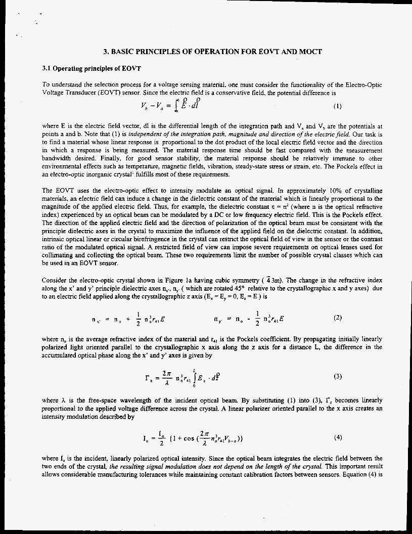
3.1 Operating principles of EOVT
To understand the selection process for a voltage sensing material, one must consider the hnctionality of the Electro-optic Voltage Transducer (EOVT) sensor. Since the electric field is a conservative field, the potential difference is
Vh - V, = [i!?.df (1)
where E is the electric field vector, dl is the differential length of the integration path and V, and V, are the potentials at points a and b. Note that (1) is independent of the integration path, magnitude and direction of the electricjeld. Our task is to find a material whose linear response is proportional to the dot product of the local elecbx field vector and the direction in which a response is being measured. The material response time should be fast compared with the measurement bandwidth desired. Finally, for good sensor stability, the material response should be relatively immune to other environmental effects such as temperature, magnetic fields, vibration, steady-state stress or strain, etc. The Pockels effect in an electro-optic inorganic crystal’ fulfills most of these requirements.
The EOVT uses the electro-optic effect to intensity modulate an optical signal. In approximately 10% of crystalline materials, an electric field can induce a change in the dielectric constant of the material which is linearly proportional to the magnitude of the applied electric field. Thus, for example, the dielectric constant E = n2 (where n is the optical refiactive index) experienced by an optical beam can be modulated by a DC or low fiequency electric field. This is the Pockels effect. The direction of the applied electric field and the direction of polarization of the optical beam must be consistent with the principle dielectric axes in the crystal to maximize the d u e n c e of the applied field on the dielectric constant. In addition, intrinsic optical linear or circular birefringence in the crystal can restrict the optical field of view in the sensor or the contrast ratio of the modulated optical signal. A restricted field of view can impose severe requirements on optical lenses used for collimating and collecting the optical beam. These two requirements limit the number of possible crystal classes which can be used in an EOVT sensor.
Consider the electro-optic crystal shown in Figure la having cubic symmetry ( 23~1) . The change in the refractive index along the x’ and y’ principle dielectric axes %., %v ( which are rotated 4 5 O relative to the crystallographic x and y axes) due to an electric field applied along the crystallographic z axis (E, = E, = 0, E, = E ) is
1 n x s = n o + - n:r , ,E 2
1 - nys - no - - 2 n:r,,E
where no is the average refractive index of the material and r,, is the Pockels coefficient. By propagating initially linearly polarized light oriented parallel to the crystallographic x axis along the z axis for a distance L, the difference in the accumulated optical phase along the x’ and y’ axes is given by
where h is the free-space wavelength of the incident optical beam. By substituting (1) into (3), rL becomes linearly proportional to the applied voltage difference across the crystal. A linear polarizer oriented parallel to the x axis creates an intensity modulation described by
where I, is the incident, linearly polarized optical intensity. Since the optical beam integrates the electric field between the two ends of the crystal, the resulting signal modulation does not depend on the length of the crystal. This important result allows considerable manufacturing tolerances while maintaining constant calibration factors between sensors. Equation (4) is

an even function centered on Vb.a=O, and is unsuitable for measuring voltages. By adding a quarter wave plate to the optical path between the two polarizers, (4) becomes sinusoidal. The output signal varies in a linear, monotonic fashion with varying voltage, provided Vb.a << VX where
is a measure of the vx = - 2 n h
X’
/1
modulation efficiency of an electro-optic material.
Table 1 lists the Pockels coefficient r41, refractive index no, the VX voltage and temperature - dependence of no for a number of cubic ( 4 3 9 crystalline materials‘.’. Also listed are some typical peak-to-peak voltages present on a power line and the resulting total peak-to-peak cycles N, for the longitudinal Pockels cell configuration described above. A serious difficulty emerges from this table. None of the common materials listed can satisfy VbS << VX. Other factors influencing the choice of sensor material include:
Z
I L v, I Polarizer
@@ Cosine Channel 5060 Beam Splitter
B x 114 Plate
Polarizer
Sine Channel (b)
Figure 1. Longitudinal Pockels cells for measuring voltage.
1) High strength and a small stress-optic coefficient are desirable to minimize the effects of thermal or vibration induced strain birefringence on sensor accuracy.
2) A small temperature dependence of the rehctive index is desired to maintain calibration over temperature. 3) A low thermal expansion coefficient ensures that optical alignment is not lost over wide temperature variations. 4) Dispersion of the Pockels constant and the refractive index must be low to minimize calibration errors caused by
changes in the light source spectrum. 5) Low costs for raw materials, ease of crystal growth and machininglpolishing complete crystals are required. 6) Reproducibility between sensors from different manufacturing runs places demands on material homogeneity and purity. 7) A high bulk resistivity is required to prevent thermal breakdown at high temperatures (see below).
After considering all of these issues, the ability to control the material composition and purity in a manufacturing environment, together with reasonable material and processing costs, led us to select (Bi 4Ge3012) for the sensor element.
Material
GaAs
Bi4Ge3Ol2
ZnSe
CdTe
GaP
n, @ A (nm) p o & ~ coeff E@ 1 kffz r41 (I@”m/c3 3.43 GI 1150 1.43 E = 13 2.07 63 850 1.03 E = 16 2.60 @, 633 2.0 c = Q
= 10 + 1 .3~10-~ OR‘
I
N1a= vp- 1 2 v, Nm= Vpk-pJ 2 v* for 161 kY line 13.2 45.2
6.0 20.5
29.2 100
53.1 183.7
15.0 51.4
for 550 k V line
Table 1. Selected properties of ( 3 3m ) electro-optic crystals.

In order to preserve the desired line-to-ground measurement capability of the optical voltage sensor and provide an accurate representation of the applied voltage, a nonpolarizing 50150 beamsplitter can be added at the output of the crystal, as shown in Figure lb'q4. The transmitted beam passes through a suitably oriented quarter- wave plate and linear polarizer to generate a sinusoidal signal biased at its midpoint with no applied voltage. The reflected beam passes through a linear polarizer, creating a cosinusoidal signal biased at its maximum transmission with no voltage amplitude, these two signals are 90" out of phase with respect to each other; while one signal is changing approximately linearly with voltage, the other signal is passing through a tum-around point. When the slope of the applied voltage ramp changes sign, the phase reiationship between the sin and cos signals flips by 180'. These two features allow complete reconstruction of the applied voltage. The detected signals are first normalized in amplitude by noting that the average of the sin signal is ( 1 , ) = I, , and the peak
value of the cos signal is = 1, , both of which are independent of voltage. Two threshold levels are used to
determine 1) how many cycles have been detected in the sin or cos signal; 2) the sign of dV/dt; and 3) whch signal and what signal polarity to use as the output signal. As shown in Figure 2, an increasing voltage ramp creates a series of sinusoidal cycles which are tracked by an up-down counter whose direction of count is determined by the relative phase between the two detected signals. The counter output is then a rough approximation of the applied voltage. The actual sin and cos signals are used to refine this approximation. Since sinxzsx introduces errors of >lo% near the threshold levels, higher order terms in the Taylor expansion of sin x are incorporated into the design to improve accuracy. All of the computation is performed by a Field-Programmable Gate Array having a total signal delay of <5 psec.
Thresh
a function Of Figure 2. Intensity modulated waveforms versus applied voltage.
2
The temperature dependence of the voltage sensor is a concern when 0.2 % accuracy over a temperature range of -50 "C to + 105 "C is desired. The expected temperature dependence of the device is
The first term indicates the effect of a temperature dependent optical source wavelength. The second and third terms define the effects of the temperature dependent refractive index and Pockels coefficient, respectively. Sbce all of the materials in Table 1 have appreciable temperature dependencies, we use a separate temperature sensor at the EOVT sensor location to electronically compensate the output signal. Electronic compensation is also used for the optical source wavelength variation with temperature.
Thermal breakdown can occur in materials having a resistivity which decreases with increasing temperature. Under normal operating conditions, both resistive and capacitive currents flow through the sensor element at 50 or 60 Hz. The resistive current contributes to Joule heating of the crystal. This heating in turn causes the resistivity of the crystal to decrease, exacerbating the heating effect. Heat loss primarily by convection through the surrounding gas and radiation to the surrounding conbiner/enviroment results in a steady-state operating temperature for the sensor element. Because of the extreme temperature requirements and the need for a f ~ t e size crystal to limit cost and optical beam path length within the crystal, a high room temperature resistivity is required to rule out the possibility of thermal breakdown. For example, an SF6- immersed, 10 cm long, 2 cm diameter Bi,Ge,O,, crystal connected to a 170 kV power line must have pRT > lo', nc rn to ensure safe operation at 105 O C ambient temperature. This requirement eliminates the use of most visible or infrared bandgap semiconductor materials because sufficiently high bulk resistivity cannot be achieved
3.2 Operating principles of MOCT

The Magneto-optic Current Transducer (MOCT) exploits the Faraday effect in a diamagnetic material to provide precision measurements of curren?. Ampere's law states that
where i is the current enclosed by the loop integral and H is the magnetic field present in the region of integration. A material for an optical current sensor must therefore modulate an optical beam in proportion to the magnetic field parallel to the beam path. The Faraday effect in diamagnetic materials provides the desired mechanism. The bound electrons in a diamagnetic glass interact with an imposed magnetic field by traversing circular paths about an axis parallel to the applied field. The electron motion results in circular birefringence, the magnitude of which is proportional to the applied magnetic field strength. When linearly polarized light is incident on a material, the plane of polarization continuously rotates as it propagates through the material, according to
where 0 is the rotation of the plane of polarization after traversing the material, V is the Verdet constant for the material, p is the magnetic permeability of the material and L is the path length. The total rotation of linearly polarized light encircling a conductor carrying current i is found by combining (6) and (7), giving B = p W i , where N is the number of optical round trips. If a linear polarizer oriented at +45O to the launched polarization axis is placed after the material, then the resulting intensity modulated signal can be written
1 0 I, = -{1 + sin(2pVNi)) 2
where I, and I,,, are the incident and modulated optical signals, respectively. Equation (8) is independent ofthe geomew of the optical path inside the material, its distance from the current carrying conductor, or any magnetic fields created by nearby currents.
Table 2 lists some typical diamagnetic materials which may be used to fabricate optical current sensorss. Listed are the Verdet constant, the refractive index, the temperature dependence of the Verdet constant, the current required to induce an optical rotation of &dl0 (approximately the linear range of the sensor), and the stress-optic coefficient. Paramagnetic materials have large temperature dependent Verdet constants and were not considered for this application.
Material
SiO,
ZnSe
BW%l
SF-57
SF-6
BK-7
". 63 ;Ifnm) 1.45 @ 852
2.60 @ 633
2.54 Q 633
1.82 @ 852
1.78 @ 852
1.51 @ 852
1 av Stress-optic coeff - -(%--', dtieakAmps1 V('7cm.T) V d T N=l, &dl 0 C (1 0'' m'm)
A (nm) @ A hm) e 2 (nm) 63 A (nm) 2.1 @ 633 2.2 x lo4 @ 633 68.2 kA @ 633 -3.36 @ 633 1.2 Q 850 119kA@850 67.6 @ 633 1.4 x lo4 @ 820 2.1 kA @ 633 --- 16.5 Q 633 2.8 x lo4 @ 850 8.7 kA @ 633 --- 11.5 @ 633 2.8 x lo4 @ 633 12.5 kA @ 633 0.03 @ 589 3.8 @ 1060 10.3 @ 633 cO.9 x1044@ 870 13.9 kA @ 633 0.63 @ 589 3.5 @ 1060 2.3 @ 633 --- 62.3 kA @ 633 2.74 @ 589 1.0 @ 1060
37.7 kA @ 1060
40.9 kA @ 1060
143 kA @ 1060
Table 2. Properties of diamagnetic materials (ppJ for bulk optical current sensors.

The following factors must be considered when selecting a sensor material:
1) A large Verdet constant is not desired when designing an optical current sensor for utility applications, because very small load currents (<I Ampere) and very large short circuit currents (>lo0 Mmpere for N.1 seconds) must be accurately measured by the same device.
2) A small stress-optic coefficient is desirable to minimize the effects of thermal or vibration induced strain birekngence on sensor accuracy. Strain applied to the sensor material can induce linear birefnngence with a value An=CP, where P is the applied pressure and C is the stress-optic coefficient in m’N. For this reason the leaded glass SF-57 has been used for optical current sensors because of its low stress-optic coefficient.
3) A small Verdet constant temperature dependence is desired to maintain calibration over wide temperature ranges. ,
4) A low thermal expansion coefficient ensures that optical alignment is not lost over wide temperature variations. 5) Dispersion of the Verdet constant must be low to minimize calibration errors caused by changes in the light source
spectrum. 6) Low costs for raw materials and machining/polishing complete sensors is required. 7) Reproducibility between sensors from different manufacturing runs is also required, placing demands on material
homogeneity and purity.
After considering all of these issues, the ability to control the material composition and purity in a manufacturing environment, together with reasonable material and processing costs, led us to select fused silica (SiO,) for the sensor element.
4. PRACTICAL ASPECTS OF OPTICS
4.1 EOVT
A practical EOVT sensor structure is shown in Figure 3. The optical path has been folded back by a right angle prism located at the high voltage end of the crystal, halving V, and allowing the fibers to connect to only the grounded end of the crystal. One fiber provides light to the sensor, and two fibers provide a return path for the two modulated signals. Optical GRIN lenses provide collimation and collection of light from 623125 pm standard telecommunications fiber. Optical components and adhesives are selected to be compatible with a wide temperature range and a potentially corrosive, extremely low humidity environment. Assembly also requires careful attention to the thermal expansion coefficients of all materials to avoid undesirable thermal stress. Extremely robust bonds are required to ensure sensor survival during lightning impulses. Since electro-optic materials are piezoelectric, large voltages having high rates of change can induce large amplitude acoustic modes in the crystal. High frequency radial modes can provide sufficient shear forces to cleave bonds. These acoustic shock waves also impose intrinsic material strength requirements for the sensor and limit the length to diameter ratio for the sensor.
............................................................................................................................ -------------------------
............................................................................................................................
Figure 3. Schematic drawing of EOVT sensor element.
The EOVT is in the process of being commercialized. Due to the limited number of sensors assembled and the limited number of field triais, the manufacturing issues associated with this technology have not been stabilized. Recently a number of sub-assembly quality tests have been recommended to ensure a high quality finished product with minimal re-work. The electro-optic crystal is the ‘Achilles heel’ of the EOVT and quality checks on this critical component were recognized early in the development phase as being critical to product success. Crystal quality checks include:

1. visual check for scratches, chips, bevels, inclusions, cracks, all of which compromise the integnty of the dielectric withstand capabilities of the fmished product. measure the resistivity of the cylindrical rod at room temperature. measure the resistivity of conductive coatings on the ends of the crystal to ensure uniformity and correct thickness. check the orientation and magnitude of the optical birefringence through the crystal to ensure correct crystal alignment. Periodic x-ray Laue images ensure that birefimgence measurements indicate the crystallographic orientation of the sample.
2. 3.
4.
Temperature cycling performance of the EOVT is still under investigation. A recent temperature run has verified a temperature stability of approximately 1.5%/100 O C , which agrees with measurements reported'. With a separate temperature sensor for compensation, the resulting system performance is as shown in Figure 4. This data was recorded by temperature cycling the sensor while maintaining the electronics at room temperature. The sensor was mounted in a small insulated chamber filled with a slight positive pressure of SF, gas to provide dielectric integrity up to 50 kV rms. The test assembly was designed for production use.
4.2 MOCT
1
0.5 L
2 I2 c 0
P X X - 0" O r -
-.
+ 0 0
0
-1 i 48 50 52 56 58
AC Voltage (kV rms)
Figure 4. Temperature cycling data for the EOVT sensor.
The optical path in the sensor material must follow a circular path about the conductor, yet introduce no additional birefrrngence into the beam. To accomplish this, the sensor design shown in Figure 5 is used. A block of glass is machined, finely annealed to remove strain birefringence, and optically polished. A parabolic reflector is used to collimate the optical beam leaving the optical fiber. The collimated beam passes through a linear polarizer and enters the main sensor block. At each comer of the sensor block a pair of mirrors deflect the beam 90". The complementary mirror pair is required to maintain the polarization state of the light at each right angle bend in the sensor. After making a round trip in the glass, the beam is passed through a second polarizer and focused by a parabolic reflector onto a receiving optical fiber. The hole in the middle of the block permits the passage of the conductor through the optical loop formed in the sensor material. Precision machining of the block is required to maintain accurate alignment between the two 200 pm core fibers and minimize insemon loss variations with temperature.
The temperature dependence of the normalized sensor output (Norm = ACDC) is given by
which includes the temperature dependence of the Verdet constant, the effect of a temperature dependent optical source wavelength and the effect of a temperature dependept circular birefringence 8. The wavelength dependent terms are electronically compensated by measuring the temperature of the light source. The remaining terms can balance each other by adjusting the temperature dependent circular birefringence 0 in the optical path between the two polarizers. This approach can yield temperature compensated sensors with registration variations of <0.3% over a 135 "C temperature span.
The complementary mirrors at each corner of the sensor are coated with a reflective film to avoid optical losses due to water condensation on these surfaces. The mirrors must be carefully matched to avoid the introduction of additional birefringence in the beam path. This sensor typically has an optical
Figure 5. Schematic drawing of MOCT transducer.

insertion loss of 10 dB, a spectral passband of >300 nm and a sensitivity of approximately I, / I, = 2.5 x The electronics interface to generate a signal representing the primary current must have very good noise performance to measure small modulations at low primary currents. It must also compensate for intensity fluctuations caused by fiber bends, vibrations, light source variations, sensor temperature induced insertion loss changes, partial failure of fiber connectors, etc. This is accomplished by taking advantage of the AC modulation superimposed on a DC background, and the non-reciprocal nature of the Faraday effect. The light source and detector electronics are designed to operate at the shot noise limit. This is necessary to accurately measure low currents with high accuracy. Even with this performance, some white noise persists on the output waveform due to the finite optical power available from commercially available LEDs. The DC background is electronically normalized, automatically controlling the gain for the AC modulation component. To cancel the effects of vibration and dnft, two counterpropagating signals are sent through the sensor element and detected. The two received signals have complementary modulation waveforms. By subtracting the two signals from each other, the signal due to the Faraday effect is doubled in amplitude and any reciprocal optical modulation due to vibrations and dnft is canceled. This approach provides excellent noise immunity under >50 g shock testing.
Ampere-'.
The MOCT design has been commercially produced for the past two years. The transition from development project status into commercial production required solving many issues associated with reproducibility, cost reduction of materials supplied by sub-contractors, streamlined calibration procedures, defintion and implementation of routine dielectric tests and the development and implementation of quality verification processes leading to IS0 9001 certification. Some of these issues are described below.
Early in the development process the temperature dependence of MOCT sensors varied dramatically, sometimes by >5%/100 "C. These early sensors required a separate temperature measurement to electronically calibrate h s error. An early decision was made to reduce the calibration error by assessing the cause of the temperature errors and systematically eliminating it. Fine annealing coupled with careful selection of the light source vendor was found to alleviate most of the temperature variation. As part of the routine calibration procedure, however, a thermal cycling run is performed on each sensor while it is connected to its corresponding electronics interface. This procedure was instituted as a quality control check to verify temperature stability, rather than as a means to correct temperature variations in calibration. A sample of the output data from a temperature run is shown in Figure 6 for three sensors to show the typical variations seen in temperature stability. Recent manufacturing data indicates that variations of <0.5%/1OO "C can be reproducibly achieved.
Optical component cost reduction was targeted as a critical issue for commercial production, whle simultaneously trying to i p r o v e sensor quality. This was accomplished by moving to an optics machining and polishing house with many years of experience machining large quantities of high quality optical lenses and prisms. The coatings applied to the sensor body were performed on a small quantity basis, and thus were very expensive. A new coating supplier was evaluated to produce larger quantities of coatings at lower costs. The final assembly of the sensor element, a process critical to achieving temperature stability and low insertion loss, was brought into the manufacturing plant to provide better control over product quality and cycle time. The light source used was re-evaluated, and a more expensive source was selected to provide a higher optical power loss budget and ',better sensor temperature characteristics. Finally, a smaller core optical fiber was selected to improve vibration induced noise immunity, reduce cabling cost, allow use of high quality FC style optical fiber connectors and allow the use of standard optical components in the dual- direction noise canceling electronics design described earlier. These changes took almost two years to implement, but have resulted in a sensor cost reduction of a factor of three over the low volume sensor cost.
100.6 1
100.4
100.2
5 100
g 99.8
99.6
h
v h0
s L
0
Figure 6. Typical thermal data run for MOCT sensors.

The time and skill level required to calibrate a complete MOCT system was much too expensive during the development phase of the product. An approach to reduce this cost has resulted in the design and assembly of several calibration stations. A temperature cycling station has two separate temperature cycling chambers, one for the electronics package and one for the current sensor elements, which are mounted on a current-carrying conductor bar. The current is measured using a separate, precision-calibrated CT. A stiff voltage source provides the reference voltage for two NIST-traceable Power Meters, one using the CT output and the other using the MOCT electronics output. The ratio of the resulting pulse counts over a specific time interval is a measure of the relative calibration stability of the MOCT relative to the CT. A I,abviewTM-based program first temperature cycles the sensors followed by the electronics. The collected data from the second temperature run is used to generate a temperature compensation table which, once loaded into the electronics package, provides a stabilized temperature performance as verified by a second temperature cycling of the electronics package.
Following this procedure, the sensors are mounted on a conductor forming a closed loop with a high current step-down transformer capable of generating up to 8 kA rms on a continuous basis. Using the same calibration technique described above, a series of calibration measurements are made at unity and f0.5 power factor, for a variety of currents from 1 Amp up to twice the rated maximum current. The calibration is also measured as a h c t i o n of the optical attenuation in the loop. A correction table based on these measurements provides an electronic correction for the light source drive current.
5. DIELECTRIC AND MECHANICAL STRUCTURE
5.1 Overview of standards and requirements
The MOCT and EOVT concepts can be readily demonstrated in the laboratory. However, transitioning these sensor technologies into actual products suitable for service on a utility power grid is a difficult undertakmg. The IEEE and IEC standards for conventional and electronic instrument transformers 6.7.8 prescribe a number of severe dielectric tests which require the device to withstand electrical stresses far beyond normal operating conditions. Furthermore, the sensor and packaging must be designed to survive extreme mechanical forces resulting from weather conditions, seismic activity, shipping and high-current faults on the power system. Finally, the current and voltage transducers must be calibrated using NIST traceable equipment to demonstrate metering accuracy.
Utility customers are traditionally very conservative with regard to new equipment and these practical issues must be addressed prior to acceptance of the technology. A typical set of requirements are presented in Table 3 for a 345 kV instrument transformer. Note that the dielectric testing and mechanical standards are essentially the same for a free-standing voltage transformer, current transformer or combined unit. These specifications were defined by agreement between ABB and the New York Power Authority for the fmt prototype 345 kV EOVT units .
The basic impulse level (BIL) is defined for the application by industry standards and is representative of the voltage transient created by a lightning strike on the power system. The chopped wave has a 15% higher crest value, but the voltage is collapsed just past the peak by means of an external rod gap in order to evaluate the device response to a fast dV/dt transient. In contrast, switching impulses are much slower than the lightning impulse waveforms and evaluate the air- insulated portion of the dielectric envelope under wet conditions. The AC withstand test demonstrates that the device can survive short-term power frequency overvoltages resulting from system faults. Partial discharge testing is performed immediately after the withstand test once the voltage is lowered to 120% of the nominal level and serves to identify defects
Rated Voltage BIL
Chop Wave Test Wet Switching Impulse
AC withstand '
AC Partial Discharge Accuracy Class
.
345 kV rms (line-to-line) => 200 kV rms (line-to-ground) 1300 kV peak (1.5 psec rise time, 50 psec to half peak) 1500 kV peak (1.5 psec nse time, chop at 3 psec ) 825 kV peak (250 psec rise time, 2500 psec to half peak) 575 kV rrns for 1 minute (line-to-ground) Less than 5 pC at 120% of rated line-to-line voltage. 0.3, + 18 minutes from 90% to 1 10% of nominal voltage
in the dielectric structure. Seismic and mechanical requirements are less
between depending On location. The
structure is typically designed to withstand the forces hurricane winds acting in concert with short circuit forces on the bus to which the device is attached. Mechanical 1500 lbs cantilever force (pull test)
and
,
Seismic 0.2 g's
Temperature Range -30 degrees C to +50 degrees C
Table 3. Standard requirements for 345 kV instrument transformer.

In the context of this paper, all discussions of insulation and mechanical structure will focus upon the EOVT. In the case of the free-standing MOCT, the sensor element is not electrically stressed and the unit can be mounted on a commercial insulator column. The combination voltage and current sensor utilizes the EOVT insulation structure to support the MOCT head in a similar fashion. Thus, the only dielectric challenge for the MOCT is the process of transitioning the signal fibers from line potential to ground. This will be discussed briefly in the context of the OMU application.
5.2 EOVT sensor element package
Having defined the relevant specifications, implementation of the BGO sensor element may be addressed. The primary issues are proper grading of the electrical stresses across the crystal and adequate shock mounting of the BGO and associated optics. Line voltage must be applied between equipotential surfaces on each end of the sensor crystal in order to obtain the required measurement accuracy. However, to ensure safe shipping and service of the device, the BGO must withstand impacts from any direction and hence must be mechanically decoupled from the support structure. These requirements are rather contradictory in nature and ultimately led to a modular approach for both the sensor element and packaging of the measurement gap. The complete sensor element package consists of the BGO crystal and optical assemblies, mechanical damping medium, structural insulator and shielding electrodes as illustrated in Figure 7.
Sulhr hexafluoride gas was selected as the dielectric medium in order to combine excellent insulating performance and material compatibility along with power industry acceptance. SF6 is commonly used for high voltage circuit breakers and gas insulated substation applications and has been very well characterized. Hence, the critical aspects of the sensor module dielectric design were the BGO crystal and BGO-SF6 interface. The latter issue is quite serious given the relative permittivity mismatches between BGO (Er = 16) and SF6 (Er =1) which will cause difficulties at locations where the crystal, gas and mounting electrodes converge. These so called “triple points” provide significant electric field enhancements by enforcement of continuity across the material boundaries. In traditional high voltage designs utilizing SF6 with epoxy insulators, the worst-case permittivity mismatch is roughly 6: 1 and shielding electrodes are employed to ensure that the triple point stresses are on the order of 20% less than the local electrode surface fields. With the substantially higher mismatch of BGO, triple point shielding factors of better than 200% are necessary for a conservative design.
The use of electrodes mounted directly to the crystal ends was thus adopted in order to provide the best possible triple point shielding. Electrically conducting clear windows are utilized over the optically active cross sections on each end of the BGO. The remaining annular regions of the crystal ends are used for bonding to the shielding electrodes using a conductive adhesive. In this manner,- precise equipotentials are defined across each end of the sensor element and the dielectric domain is effectively bounded. As previously discussed, BGO is piezo- electric in nature and the correct bonding scheme is essential to prevent mechanical resonance problems during the application of impulse test waveforms which can excite fkequencies up to 1 MHz. If such resonance is not properly damped, the crystal ends may delaminate and cause catastrophic dielectric failure. Note that flexible wires are used to make hard electrical connections between the main support electrodes and sensor element electrodes.
Prior known applications of BGO have not utilized the material as a highly stressed dielectric and virtually no high voltage design data was available for the bulk material. Early breakdown tests of very small samples suggest that BGO can withstand internal electric fields up to 20 kV/mm under impulse conditions. This limited date provides some indication of the design stress limit and hence required sensor element length. The final component of the dielectric design is the structural insulator which provides mechanical strength and ensures precise alignment of the aluminum shielding electrodes. These parts have been made using both cast
Connecting
wire -A
High Voltage Electrode ,
Figure 7. Illustration of EOVT sensor module concept.

cycloaliphatic filled epoxies and filament-wound epoxy cylinders whch are capable sustaining the electrical stresses required for various BGO sensor lengths of interest. In the former case, properly shaped mounting hardware is cast into the cylinder ecds to provide a means of mounting to the electrodes. The filament-wound cylinders are simply glued to the end electrodes with a large bonding area employed to provide high strength.
Dielectric design optimization was performed using Flux 2D9 for finite element analysis of the electrostatic fields in the cylindncally symmetric geometry. Following traditional practice, the design stresses were evaluated at the chopped wave crest voltage (i.e. 1500 kV for the 345 kV device in Table 3) and the BGO bulk stresses were fixed well below 20 kV/mm to allow for scaling effects. The SF, volume and electrode surface stresses were defined based on a breakdown field of 9 kV/mm/bar (absglute pressure) with a comfortable safety factor for nominal operating pressure. Multiple iterations were required to optimize the geometry and minimize the amount of BGO required to reduce cost. Most gas-filled devices are typically equipped with pressure alarms which trip at set points below the nominal level. All designs were based on the second level alarm pressure below which the unit would be removed from service. For the 345 kV units discussed in Table 3, the nominal operating and second alarm pressures are 60 psig and 50 psig respectively to provide an additional 20% safety margin.
Shock mounting of the BGO crystal and optics is achieved using a highly purified open-cell silicone foam which does not outgas. The foam is supplied in sheet form and stamped into the desired annular shapes needed for radial and axial damping. Note that the optics housings on each end of the crystal are of the same dimensions such that the sensor element is mechanically symmetric. The acting area and thickness of the foam are defined based on the worst-case design force in a given direction, the effective mass of the sensor element and the nonlinear spring constant characteristic of the foam. In response to a mechanical shock, the sensor element will act to compress the foam until the knee of the spring constant versus compression curve is surpassed and a significant restoring force occurs. Ideally, the shock energy should be dissipated in the foam before the sensor element is damaged by the restoring force of the foam or impact with the main gap electrodes. This shock mounting scheme has been demonstrated to be exceptionally reliable despite severe sue limitations on the amount of silicone foam used. Sensor element assemblies of various lengths have survived transport despite having received monitored impacts of greater than 4 g’s.
In the case of the OMU application where an MOCT sensor is mounted on the high voltage terminal of the EOVT, some provision must be made for transitioning the MOCT signal fibers to ground potential. l h s problem can be solved in a number of different ways and several schemes have been proven effective. The most basic approach is to run bare fibers across the gap in a Iow field region with a weak tensile force applied to keep them parallel to the module axis. The fibers are transitioned into the gas gap through small holes with the curved edges to provide triple point shelding. When mechanical support of the fibers is necessary they can be cast into a silicone rubber support cylinder which is implemented in a similar fashion. Note that the fibers are run inside the high voltage and ground conductors on either side of the gap.
5.3 Prototype dead tank implementation
The sensor module and measurement gap geometry discussed in the previous section represents only one aspect of the complete device. A suitable dielectric envelope is required in order to contain the SF, gas and meet the insulation requirements for atmospheric air. Furthermore, this enclosure must allow for high voltage connections, high-pressure gas safety hardware and mounting on a suitable foundation structure. Existing ABB technology for gas insulation substation components was selected to fabricate the fmt prototype units for optimal simplicity, reliability and delivery time.
A “dead tank” device is named for the grounded metal enclosure which encloses the voltage transformer hardware as illustrated in Figure 8. This type of codiguration is commonly used for conventional instrument transformers and utilizes a bushing to transition line voltage into the grounded tank were the measurement device is located. Electrical connection to the power line is made using a NEMA pad built into the shield at the top of the bushing. The prototype design incorporates a tapered aluminum pin whlch mates with the high voltage bushing conductor via a helical contact spring arrangement. This contact scheme allows for mechanical movement of the bushing without mechanical forces acting on the module assembly. Note that the support module electrodes in this case require large outer radii to control the electric field between the high voltage terminal and grounded enclosure. The EOVT module is mounted to the bottom hatchcover plate and assembly is undertaken using customized lift tables to insert the module into the main aluminum tank from below. A rupture disk assembly is required on the tank in order to provide a safe path for venting the internal gas if excessive pressure occurs.

Composite bushings were selected for the prototype EOVT units for a number of practical reasons. Conventional porcelain bushings of the size required are extremely heavy and somewhat vulnerable to chipping during handling. Furthermore, in a pressurized application, porcelain may generate shrapnel in the event of a dielectric failure during type testing or service. Modem composite insulators are made using filament wound epoxy shells for structural support. The epoxy is covered externally with silicone rubber weather sheds to control water flow and extend the electrical surface creepage distance under wet conditions. The bushing is mounted to the device using cast aluminum flanges which are glued to the epoxy shell. This type of insulator is quite safe and will not shatter even when punctured by an electrical arc at full pressure. The bushing and tank share common SF6 with the EOVT module and must thus be properly designed to function at the corresponding pressure. The most critical dielectric aspect of the main structure is the “throat” region where the high voltage conductor penetrates the grounded tank. As shown in Figure 8, an internal grading shield is required to control both the internal and external electric fields near the transition. The relatively high internal stresses are easily withstood by the high pressure SF6 gas insulation and the external stress peak near the throat shield actually represents the weakest point. Note that the high voltage conductor represents a fixed equipotential which effectively minimizes the external electric fields over most of the bushing length.
iJ Line
Filament Wound
Figure 8. Dead tank EOVT concept drawing.
5.4 Next generation live tank implementation
The first prototype design was a complete success and provided a basis for cost assessment and reduction. Ultimately, the main enclosure was identified as a significant portion of the material cost and a more advanced concept was required to make the technology commercially competitive. Manufacturing complexity dictates that the price of a composite bushing insulator increases dramatically with diameter. However, the throat region stress levels in the dead tank scheme defme a limit for the minimum insulator diameter which is too costly. This problem coupled with the expense of the tank prompted development of a “live tank” approach where the EOVT module is mounted directly inside the insulator column. The throat region is thus eliminated and the requisite air stress design criteria can be met using a smaller diameter insulator shell. A generic design strategy was adopted such that EOVT systems ranging in voltage class from 115 kV to 550 kV could be fabricated using optimized common parts with the measurement gap and insulator column length as the only variables.
The sensor module design for the live tank approach is quite similar to that described previously and is implemented as shown in Figure 9. Further optimization of the shielding electrodes combined with increased operating pressure allow the use of reduced BGO crystal lengths for the various voltage ratings. Scaling of the gap to different sizes is readily achieved using wet filament wound epoxy cylinders which can be bought in standard pieces and cut to length. Elimination of the grounded enclosure significantly reduces the size of the main electrode shielding radii and the overall module diameter can be reduced by more than a factor of two. This modification reduces the weight and size of the sensor element package to the point that direct mounting to the high voltage conductor is possible. Furthermore, the total mechanical moment of the sensor package and high voltage conductor is small enough that the device can be shipped M y assembled which was not possible for the dead tank design. The ground connection to the module is made using a thin-walled aluminum pipe and helical contact spring to provide flexibility.
The cost of composite insulators can be dramatically reduced by purchasing in large quantities. However, this poses a problem when a variety of insulator heights are needed for the various voltage classes. This dificulty is overcome by selecting a standard insulator size for the 115 kV O W which can be used as the basic building block for the higher voltage designs as illustrated in Figure 10. The top and bottom end flanges are specified so that any number of these insulators can be stacked together to obtain the required air strike and creepage distances between the power line and ground for a given voltage rating. When multiple insulators are used, any mating flanges in the middle of the stack will float electrically with their potential determined based on capacitive coupling. This feature can be utilized to dramatically improve the external

Figure 9. Concept drawing of live tank OMU.
dielectric withstand capability. Optimal placement of the Floating Flange Pain
measurement gap combined with the capacitive grading effect from the floating flanges has been demonstrated to provide an extremely robust design which outperforms the dead tank structure under both lightning impulse and wet switching surge conditions. The limiting factor for the live tank
configuration is the external air stress on the insulator weathersheds in the measurement! gap region. The stacked insulator concept has been demonstrated using as many as three of the 1 15 kV standard insulators for voltage ratings up to the IEC 420 kV class. In order to achieve 550 kV a larger insulator diameter is required to maintain safe external stress levels. However, the live tank insulator for this case can be made using standard tooling and is still much smaller and cheaper than the corresponding dead tank size.
1 I5 kV Single 230 kV Double 345 kV Triple Stack Stack Stack
Figure 10. Insulator building block approach for various vo%!e classes showing optimal modult Placement.
5.5 Type testing of prototypes
All of the EOVT and OMU units described in this paper have been fully type tested in accordance with IEEE Standard 4'' at the NEETR4C High Voltage Laboratory affiliated with the Georgia Institute of Technology. The high voltage tests discussed in the first section were performed to the specified levels under the following protocol:
I. Service voltage < 345 kV: 1 full wave lightning impulse, two chopped wave lightning impulses, 14 full wave impulses, AC withstand (dry) followed by partial discharge measurement, AC wet test.
11. Service voltage 2 345 k V 1 full wave lightning impulse, two chopped wave lightning impulses, three full wave impulses, AC withstand (dry), AC partial discharge, 15 wet switching impulses.
All EOVT units were calibrated using a precision NIST traceable wound potential transformer in conjunction with appropriate volt and phase meters to demonstrate 0.3% accuracy, At present, designs have been successfully type tested for the following voltage classes:
I. Dead tank => 145 kV, 161 kV, 345 kV and 420 kV.
11. Live tank => 115 kV, 138 kV, 230 kV, 345 kV, 420 kV and 550 kV.
Additional testing was performed on the 345 kV prototype units specified in Table 3 at the IREQ laboratory in Quebec'* unit was subjected to complete thermal cycling at rated voltage to verify temperature compensation of the EOVT. The mechanical response of one device was evaluated on a shake table subject to the specified forces. The frequency response was shown to be nearly identical to that measured for the composite insulator by the manufacturer. Both of these tests were considered successful and provided further justification for customer acceptance.
9 H v / t ' " 4 I

6. ELECTRONICS AND INTERFACING FOR METERING/PROTECTION
The user expectations for non-conventional voltage and current sensors are that existing metering and protection applications will operate with these devices. Furthermore, both conventional and unconventional units should be able to function together, preferably on an interchangeable basis. Meeting this expectation, without some limitations is unfortunately not realistic. This is illustrated in Table 4 which compares some of the basic measurement requirements for current and voltage in each of the applications.
When these requirements are taken together, they represent a significant design problem for the electronics, both from the aspect of dynamic range and for interfacing to all vintages of utility equipment. While equipment has been designed and tested which is capable of meeting these requirements, it is generally too expensive to be of practical use. In addition, there are issues of long-term stability, performance at temperature extremes, signal reproduction fidelity, and the ability to distinguish between signal and noise which must be taken into consideration.
This topic is too lengthy to be covered in this paper and much of it has been covered in the literaturei2J3J4. Essentially, while the customer expectation remains, the solution has been to require a modification of the end-use application. On one hand, this requirement for departing from the norm to accomodate unconventional devices has had the effect of slowing acceptance and created the need for field trials as a vehicle for building a performance history. Conversely, the fact that metering and protection equipment is undergoing a shift from electromechanical to electronic technology supports the future use of optical devices.
For metering, the deviation from existing practices with conventional measurement techques is a lesser problem. There exists a fully developed market for metering equipment with a rated current of 1.OA. This market is traditionally those countries that operate under the European standard (IEC) as opposed to the American standard (IEEE/ANSI). With a maximum operating current level of 2.0A and the low burdens typically presented by metering applications, the ability to generate these current signals is within the economic constraints of a commercial optical system. Also, while the dynamic range requirements are not insignificant, they are well within the capabilities of present current and voltage sensor designs.
Protection requirements are another matter. In this application, both the dynamic range for the primary signals and the burden requirements for the electronic output presents a situation whch is too complicated to be reliable and too expensive to be practical, if the interface is required to adhere to present IEC or IEEUANSI requirements. In the absence of any governing standards, two approaches have emerged in the short term and one is being considered for the longer term.
In the short term, the only practical solution is to remain with an analog interface and two designs for current sensors have been offered. The first approach provides a signal voltage interface in the range of 20OmV to 4OhV RMS at nominal current with voltages in the range of 1OV RMS for fault currents. The second alternative is to output is a low current on the order of lOmA to lOOmA at nominal primary current with a 2A maximum to handle faults. A similar approach has been taken with the signal processing electronics for voltage sensors. The result is that a modification is required to electronic relays to allow operation with these low level signals and there is a difficulty in interfacing with older electromechanical relay designs.
Taking a longer view, the digital interface becomes more attractive as substation technology advances and the issue of equipment burden is insignificant. While dynamic range is still a challenge, it is within the capability of existing signal processing technology. The digital rammeter Metering interface also eliminates the circuitry I I
', I Yrotecnoo
required to bring the interface to a
distributed throughout a utility Voltage Range 80% V nom to 120%V nom substation. However, one must still FrequencyRange expect the analog approach to remain
CWmtRange I I
robust enough level that it can be safely IO-' to 103 A io2 to 1 0 4 ~ 3%V nom to 200%V
0t01o3 HZ IO' TO i o4 VA
I 45Hz to 65Hz vA Burden capability
for a considerable period of time as the OTO 10' VA utility conversion from analog to digital operations occurs. Table 4. Voltage and current measurement requirements for metering and
protection.

7. FIELD INSTALLATIONS TO DATE
Over the last ten years a number of EOVT and MOCT sensors have been installed at utility sites in the Americas and Europe for field trials. Presently, over 150 MOCT units are in service along with 10 of the more recently developed EOVT units. Since previous papers have described MOCT system performance, we will focus in this paper on the performance of recent installations of EOVT’s.
The EOVT has been installed at system voltages of 110 kV, 161 kV, 345 kV and 420 kV, with systems soon to be delivered at 150 kV and 550 kV. Although relaying and protection is an important application for the voltage sensor, most field trials to date have been targeted for metering applications. In t l vs case, an O W , which combines an EOVT with an MOCT to optically meter power flow is required. The first utility installation of an EOVT was at 420 kV in a large substation near Karlsruhe, Germany. A more recent installation at Marcy substation near Utica, NYi5 has both MOCT’s and EOVT’s monitoring a 345 kV power line. This installation has recently been commissioned and performance data will be presented in a future paper. The single phase 420 kV EOVT has been in operation for more than one year and some data is presented on the performance of this unit.
The single phase EOVT in Germany monitors a 420 kV line carrying power from southwestern Germany into northern Switzerland. The device was completely assembled, fully type tested and calibrated against a gas-insulated class 0.3 PT which was separately calibrated to <0.1%. Following this testing procedure, the device was partially disassembled, shipped to Germany and re-assembled on site during installation. An outdoor test bay in this large substation was configured for installation of the device. The EOVT output, a reference class 0.5 PT signal, the ambient temperature and a time stamp are recorded in 15 minute increments by an electronic logger designed .and assembled at the University of Karlsruhe. The data acquisition system has a basic accuracy of 1%, a phase angle accuracy of *lo, and a long term drift stability of 1-2%. The electronics were installed in a metal hut with a heater to prevent ftost buildup in the winter, but no air conditioning was provided for summer conditions. Because of the data acquisition system’s limited accuracy, the collected data indicates trends in device performance and cannot be used as an accurate measure of the absolute calibration for the device.
Figure 11 shows the EOVT output error versus the reference PT, plotted against the outside ambient temperature, where each data point represents an average over one day of data collected in 15 minute increments. The data indicates a slight (~0.05%) variation in calibration over a 20 degree temperature variation. This small variation suggests that the temperature
1
0.95 .-
0 g
........ : ......... : ......... : ......... :- ........
................. i... .................. j .........
......... 1 ......... .......... i ......... 0.85 .... J h
V . 6\0 0 8 ..................................... : ......... L
0
LLi 0.75 __........I... .; ......... .: .......... i.. .......
..............
0.5 1 I
-5 0 5 10 15 20
Temperature (degrees C)
Figure 11. Calibration vs ambient temperature for 420 kV EOVT.
- 5 0.7 ......
0.6 ... :. . ..............................
0.5 1 I 0 25 50 75 100 125 150
Time (days)
Figure 12. Long term calibration versus time for a 420 kV EOVT.

compensation used in the sensor
errors fiom the expected value of 0.3% for an uncompensated EOVT. The output calibration as a function of time is mdicated in Figure 12. During this four- -
0 month period from September - f O through January, the ambient
temperature fell monotonically - ;r
s from approx. 20 oC to approx. 0 ~
oC. However, the dnft indicated by this graph is not monotonic, but rather indicates an initial bum-in period where the error decreases by 0.1% followed by a monotomc increase in error of -1 0.1% over the next four months of operation. The source of h s drift is still under investigation, but is likely caused by an
uncompensated temperature dependence of the EOVT electronics or long-term drift of the optical source wavelength. Given the magnitude of the errors observed the metering performance of the EOVT has been very good.
has reduced the temperature 1
v
r
Y - -0.5
- kVAR Error
19 20 21 22 23 24
Time (hours)
Figure 14, 345 kV EO- performance vs time.
Figure 13. Photograph of installed 345 kV EOVT’s.
A troubling issue with h s first EOVT installation is sensitivity to line transients. We have observed an instability in the EOVT output when the sensor attempts to track high fiequency transients normally encountered during switching operations or lightning stnkes whch renders the device unsuitable for relaying and protection use. More recent versions of the EOVT electronics have addressed this problem.
An additional installation in upstate New York is a three-phase set of 345 kV EOVT’s and MOCT’s. A photo of the EOVT set is shown in Figure 13. These devices have a high accuracy Power Measurement Unit (PMU) collecting signals from conventional CT’s and PT’s , MOCT’s and EOVT’s. Four separate class 0.3 electronic power meters record power flow to determine the metering performance using only optical devices or mixed conventional and optical devices. A meter connected with a conventional CT and PT provides current and voltage references. The PMU has a basic accuracy of approx. 0.3 % and a phase error of <O.lo. A Siemens fault locating protection relay records fault waveforms fiom both conventional and optical devices to determine the ability of the sensors in tracking current or voltage transients.
These devices have been energized for almost one year, with the data acquisition system in operation for approximately three months. Some preliminary data from this installation is shown in Figure 14. The calibration ratio is plotted versus time for a few hours of recorded data. The calibration enor is within the +1.0% allowed when comparing two class 0.3, 3-phase measurement systems. Temperature performance over a wide temperature range and long-term stability will be reported in a future paper.
ACKNOWLEDGEMENTS
The authors wish to thank the Tennessee Valley Authority, Empire State Electric Energy Research Corporation, ABB Schaltanlagen GmbH (Germany), ABB Power T&D Company (US), ABB Corporate Research (Zurich, Switzerland) and Bonneville Power Authority for their financial support of this emerging technology. The outstanding individual efforts of Scott Weikel, Jorge Amigo, Charlie Buckner, Debbie Harvell, Robert Miller, Pam Yakymyshyn, Paul Rudolph, Klaus Bohnert and Alexis Mendez are gratefully acknowledged. We are also indebted to Trans-Alta Utilities, Calgary, Canada for their significant support of the MOCT as a commercial product.
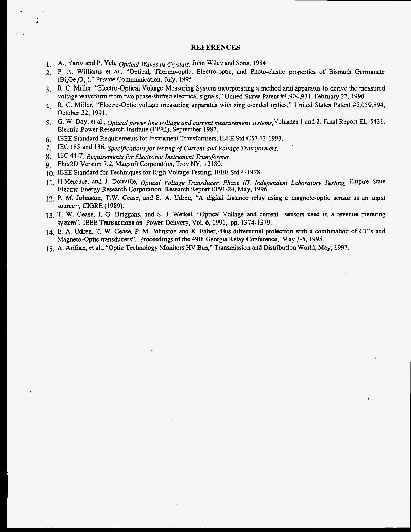
REFERENCES
1. A., Yariv and P, Yeh, Optical waves in cystals, John Wiley and Sons, 1984. 2. P. A. Williams et al., “Optical, Thermo-optic, Electro-optic, and Photo-elastic properties of Bismuth Germanate
(Bi,Ge,O,,),” Private Communication, July, 1995. 3 . R. C. Miller, “Electro-Optical Voltage Measuring System incorporating a method and apparatus to derive the measured
voltage waveform from two phase-shifted electrical signals,” United States Patent #4,904,93 1, February 27, 1990. 4. R. C. Miller, “Electro-Ophc voltage measuring apparatus with single-ended optics,” United States Patent #5,059,894,
October 22, 1991. 5 . G. w. Day, et al.9 Optical power line voltage and current measurement systems,Volmes 1 and 2, Fhal)RePofi EL-5431-
Electric Power Research Institute (EPRI), September 1987. 6. IEEE Standard Requirements for Instrument Transformers, IEEE Std (37.13-1993. 7. IEC 185 and 1 8 6 Specfications for testing of Current and Voltage Transformers. 8 . IEC 44-79 Requirements for Electronic Instrument Transformer. 9. Flux2D Version 7.2, Magsoft Corporation, Troy NY, 12180. 10. IEEE Standard for Techniques for High Voltage Testing, IEEE Std 4-1978. 1 1. H.Mercure- and J. Douville, Optical Voltage Transducer, Phase III: Zndependent Laboratory Testing, Empire State
Electric Energy Research Corporation, Research Report EP91-24, May, 1996. 12. P. M. .Joiu~ston, T.W. Cease, and E. A. Udren, “A digital distance relay using a magneto-optic sensor as an input
source’; CIGRE (1989). 13. T. W. Cease, J. G. Driggans, and S. J. Wedcel, “Optical Voltage and current sensors used in a revenue metering
system”, IEEE Transactions on Power Delivery, Vol. 6, 1991, pp. 1374-1379. 14. E. A. Udren, T. W. Cease, P. M. Johnston and K. Faber,-Bus differential protection with a combination of CT’s and
Magneto-optic transducers”, Proceedings of the 49th Georgia Relay Conference, May 3-5, 1995. 15. A. Arifian, et al., “Optic Technology Monitors H V Bus,” Transmission and Distribution World, May, 1997.