5.7 kv rms signal and power isolated rs-485 transceiver ... · energy meters . general description...
TRANSCRIPT

5.7 kV RMS Signal and Power Isolated RS-485 Transceiver with ±15 kV IEC ESD
Data Sheet ADM2867E/ADM2865E/ADM2863E/ADM2861E
Rev. A Document Feedback Information furnished by Analog Devices is believed to be accurate and reliable. However, no responsibility is assumed by Analog Devices for its use, nor for any infringements of patents or other rights of third parties that may result from its use. Specifications subject to change without notice. No license is granted by implication or otherwise under any patent or patent rights of Analog Devices. Trademarks and registered trademarks are the property of their respective owners.
One Technology Way, P.O. Box 9106, Norwood, MA 02062-9106, U.S.A. Tel: 781.329.4700 ©2020 Analog Devices, Inc. All rights reserved. Technical Support www.analog.com
FEATURES 5.7 kV rms isolated RS-485/RS-422 transceiver Low radiated emissions, integrated, isolated dc-to-dc
converter Passes EN 55032 Class B with margin on a 2-layer PCB Cable invert smart feature
Correct reversed cable connection on A, B, Y, and Z bus pins while maintaining full receiver fail-safe feature
ESD protection on RS-485 A, B, Y, and Z pins ≥±12 kV IEC61000-4-2 contact discharge ≥±15 kV IEC61000-4-2 air discharge
High speed 25 Mbps data rate (ADM2865E/ADM2867E) Low speed 500 kbps data rate for EMI control
(ADM2861E/ADM2863E) Flexible power supplies
Input VCC supply of 3 V to 5.5 V Logic VIO supply of 1.7 V to 5.5 V VSEL pin to select VISO supply of 5 V (VCC > 4.5 V) or 3.3 V
PROFIBUS compliant for 5 V VISO Wide operating temperature range: −40°C to +105°C High common-mode transient immunity: 250 kV/µs Short-circuit, open-circuit, and floating input receiver fail-safe Supports 196 bus nodes (72 kΩ receiver input impedance) Full hot swap support (glitch free power-up/power-down) Safety and regulatory approvals (pending) CSA Component Acceptance Notice 5A, DIN V VDE V 0884-11,
UL 1577, CQC11-471543-2012, IEC 61010-1 28-lead, fine pitch SOIC_W package (10.15 mm × 10.05 mm)
with >8.0 mm creepage and clearance
APPLICATIONS Heating, ventilation, and air conditioning (HVAC) networks Industrial field buses Building automation Utility networks Energy meters
GENERAL DESCRIPTION The ADM2861E, ADM2863E, ADM2867E, and the pending product within this family (light blue at the top of each page and gray in text) are 5.7 kV rms signal and power isolated RS-485 transceivers. The devices pass radiated emissions testing to the EN 55032 Class B standard with margin on a 2-layer printed circuit board (PCB) using two small external 0402 ferrites on isolated power and ground pins. The device features an integrated, low electromagnetic interference (EMI), isolated dc-to-dc converter, which eliminates the need for an external isolated power supply. The isolation barrier provides immunity to system level electromagnetic compatibility (EMC) standards. The family of isolator devices features ±12 kV contact and ±15 kV air IEC61000-4-2 ESD protection on the RS-485 A, B, Y, and Z pins. The devices also features cable invert pins, allowing the user to quickly correct reversed cable connection on the A, B, Y, and Z bus pins while maintaining full receiver fail-safe performance.
Slew rate limited versions are available, which are optimized for low speed over long cable runs, and have a maximum data rate of 500 kbps. Half duplex and full duplex variants are available. The full duplex generics allow independent cable inversion of the driver and receiver for additional flexibility.
The Pending Products section provides additional preliminary information on the following pending product: ADM2865E (see Table 22).
Table 18 shows the summary description of each generic.

ADM2867E/ADM2865E/ADM2863E/ADM2861E Data Sheet
Rev. A | Page 2 of 29
TABLE OF CONTENTS Features .............................................................................................. 1 Applications ...................................................................................... 1 General Description ......................................................................... 1 Revision History ............................................................................... 2 Functional Block Diagrams ............................................................. 3 Specifications .................................................................................... 4
Timing Specifications .................................................................. 6 Package Characteristics ............................................................... 9 Regulatory Information ............................................................... 9 Insulation and Safety Related Specifications ............................ 9 DIN VDE V 0884-11 (VDE V 0884-11) Insulation Characteristics (Pending) .......................................................... 10
Absolute Maximum Ratings ......................................................... 11 Thermal Resistance .................................................................... 11 Electrostatic Discharge (ESD) Ratings .................................... 11 ESD Caution................................................................................ 11
Pin Configurations and Function Descriptions ......................... 12 Typical Performance Characteristics ........................................... 14 Test Circuits .................................................................................... 19 Theory of Operation ...................................................................... 20
Low EMI Integrated DC-to-DC Converter ............................ 20
Robust Low Power Digital Isolator .......................................... 20 High Driver Differential Output Voltage ............................... 20 IEC61000-4-2 ESD Protection ................................................. 20 Truth Tables ................................................................................ 21 Receiver Fail-Safe ....................................................................... 22 Driver And Receiver Cable Inversion ..................................... 22 Hot Swap Inputs ......................................................................... 22 196 Transceivers on the Bus ..................................................... 23 Driver Output Protection ......................................................... 23 1.7 V To 5.5 V VIO Logic Supply .............................................. 23
Applications Information ............................................................. 24 PCB Layout and Electromagnetic Interference (EMI) ......... 24 Device Power-Up ....................................................................... 24 Maximum Data Rate vs. Ambient Temperature ................... 24 Isolated PROFIBUS Solution ................................................... 25 EMC, EFT, and Surge ................................................................ 25 Insulation Lifetime ..................................................................... 25 Typical Applications .................................................................. 26
Outline Dimensions ....................................................................... 28 Ordering Guide .......................................................................... 28 Pending Products ....................................................................... 29
REVISION HISTORY 6/2020—Rev. 0 to Rev. A Changes to General Description Section ...................................... 1 Changes to DIN VDE V 0884-11 (VDE V 0884-11) Insulation Characteristics (Pending) Section ................................................ 10 Changes to Table 8 ......................................................................... 11 Added Electrostatic Discharge (ESD) Ratings Section, ESD Ratings for ADM2861E/ADM2863E/ADM2865E/ADM2867E Section, and Table 11; Renumbered Sequentially ...................... 11 Changes to Ordering Guide .......................................................... 28 Changes to Pending Products Section and Table 21 ................. 29
5/2020—Revision 0: Initial Version

Data Sheet ADM2867E/ADM2865E/ADM2863E/ADM2861E
Rev. A | Page 3 of 29
FUNCTIONAL BLOCK DIAGRAMS VCC VISOOUT VISOIN
DE
TxD
RE
INVD
INVR
RxD
VIO
GNDISOGND1
ADM2863E/ADM2867E
RS-485TRANSCEIVER
OSCILLATOR
GND2
RECTIFIER
REGULATOR
ENCODE R
D
DECODE
DECODEENCODE
DECODEENCODE
DECODEENCODE
ISOLATIONBARRIER
CABLEINVERT
A
Y
Z
B
IEC6
1000
-4-2
ESD
PRO
TECT
ION
DIGITAL ISOLATORiCoupler
2142
9-00
1
LOW RADIATEDEMISSIONS DC-TO-DC
Figure 1. ADM2863E/ADM2867E
2142
9 -1
01
VISOOUT VISOIN
DE
TxD
RE
INV
RxD
VIO
GNDISOGND1
ADM2861E/ADM2865E
RS-485TRANSCEIVER
GND2
ENCODE R
D
DECODE
DECODEENCODE
DECODEENCODE
DECODEENCODE
ISOLATIONBARRIER
CABLEINVERT A
B
IEC6
1000
-4-2
ESD
PRO
TECT
ION
DIGITAL ISOLATORiCoupler
VCC
VIO
OSCILLATOR RECTIFIER
REGULATORLOW RADIATED
EMISSIONS DC-TO-DC
Figure 2. ADM2861E/ADM2865E

ADM2867E/ADM2865E/ADM2863E/ADM2861E Data Sheet
Rev. A | Page 4 of 29
SPECIFICATIONS All voltages are relative to their respective ground: 3.0 V ≤ VCC ≤ 5.5 V, 1.7 V ≤ VIO ≤ 5.5 V, TMIN (−40°C) to TMAX (+105°C). All minimum and maximum specifications apply over the entire recommended operation range, unless otherwise noted. All typical specifications are at TA = 25°C, VCC = VIO = 5 V, VISOOUT output voltage (VISO) = 3.3 V (VSEL = GNDISO), unless otherwise noted. All parameters are characterized with a BLM15HD182SN1 ferrite bead between the VISOOUT and VISOIN pins, and between the GNDISO and GND2 pins.
Table 1. Parameter Symbol Min Typ Max Unit Test Conditions/Comments PRIMARY SUPPLY CURRENT
VCC Supply Current—Unloaded ICC 21 46 mA VSEL = GNDISO (DE = 0 V) 28 48 mA VCC ≥ 4.5 V, VSEL = VISO (DE =0 V) 20 53 mA VSEL = GNDISO (DE = VIO) 26 51 mA VCC ≥ 4.5 V, VSEL = VISO (DE = VIO)
VIO Logic Supply Current IIO 0.65 0.9 mA DE = 0 V 5 8 mA DE = VIO ISOLATED SUPPLY CURRENT
ADM2861E/ADM2863E (Data Rate = 500 kbps)
IISOIN 50 75 VISOIN = 3 V to 3.465 V, 54 Ω between Y and Z
ADM2865E/ADM2867E (Data Rate = 25 Mbps )
55 75 mA VISOIN = 3 V to 3.465 V, 54 Ω between Y and Z
ISOLATED DC-TO-DC CONVERTER VISOOUT Output Voltage VISO 3 3.3 3.465 V VSEL = GNDISO, IISOOUT = 10 mA minimum to 55 mA
maximum1 4.5 5.0 5.25 V VCC ≥ 4.5 V, VSEL = VISO, IISOOUT = 10 mA minimum to
90 mA maximum1 Output Current Available from
VISOOUT Supply Pin IISOOUT 90 mA VCC ≥ 4.5 V, VSEL = VISO, VISO ≥ 4.5 V
VCC Minimum Start-Up Voltage VSTART 3.135 V DE = GND1, see the Device Power-Up section Start-Up Time tSTART 10 ms DE = GND1, see the Device Power-Up section
DRIVER Differential Output Voltage
Loaded |VOD2| 2.0 2.4 VISO V VCC ≥ 3.0 V, VSEL = GNDISO, RL = 100 Ω, see Figure 40
1.5 2 VISO V VCC ≥ 3.0 V, VSEL = GNDISO, RL = 54 Ω, see Figure 40 2.1 3.1 VISO V VCC ≥ 4.5 V, VSEL = VISO, RL = 54 Ω, see Figure 40
Over Common-Mode Range |VOD3| 1.5 1.9 VISO V VCC ≥ 3.0 V, VSEL = GNDISO, −7 V ≤ common-mode voltage (VCM) ≤ 12 V, see Figure 41
2.1 3.1 VISO V VCC ≥ 4.5 V, VSEL = VISO, −7 V ≤ VCM ≤ 12 V, see Figure 41 Δ|VOD2| for Complementary
Output States Δ|VOD2| 0.2 V RL = 54 Ω or 100 Ω, see Figure 40
Common-Mode Output Voltage VOC 1.5 3.0 V RL = 54 Ω or 100 Ω, see Figure 40 Δ|VOC| for Complementary
Output States Δ|VOC| 0.2 V RL = 54 Ω or 100 Ω, see Figure 40
Short-Circuit Output Current IOS −250 +250 mA −7 V ≤ output voltage (VO) ≤ +12 V Output Leakage Current (Y, Z)2 IO 1 50 µA DE = RE = 0 V, VCC = 0 V or 5.5 V, VIN = 12 V
−50 10 µA DE = RE = 0 V, VCC = 0 V or 5.5 V, VIN = −7 V
Pin Capacitance (A, B, Y, Z) CIN 28 pF Input voltage (VIN) = 0.4sin(10πt × 106) RECEIVER
Differential Input Threshold Voltage, Noninverted
VTH −200 −125 −30 mV −7 V ≤ VCM ≤ +12 V, INV/INVR = 0 V
Differential Input Threshold Voltage, Inverted
30 125 200 mV −7 V ≤ VCM ≤ +12 V, INV/INVR = VIO
Input Voltage Hysteresis VHYS 25 mV −7 V ≤ VCM ≤ +12 V Input Current (A, B) II 167 µA DE = 0 V, VCC = powered/unpowered, VIN = 12 V
−133 µA DE = 0 V, VCC = powered/unpowered, VIN = −7 V Pin Capacitance (A, B) CIN 4 pF Input voltage (VIN) = 0.4sin(10πt × 106)

Data Sheet ADM2867E/ADM2865E/ADM2863E/ADM2861E
Rev. A | Page 5 of 29
Parameter Symbol Min Typ Max Unit Test Conditions/Comments DIGITAL LOGIC INPUTS
Input Low Voltage VIL 0.3 × VIO V DE, RE, TxD, INV, INVR, INVD
Input High Voltage VIH 0.7 × VIO V DE, RE, TxD, INV, INVR, INVD
Input Leakage Current II −1 0.1 2 µA DE, RE, TxD, VIN = 0 V or VIO
−1 10 30 µA INV, INVR, INVD, VIN = 0 V or VIO RxD DIGITAL OUTPUT
Output Low Voltage VOL 0.4 V VIO = 3.6 V, output current (IOUT) = 2.0 mA, differential input voltage (VID) ≤ −0.2 V
0.4 V VIO = 2.7 V, IOUT = 1.0 mA, VID ≤ −0.2 V 0.2 V VIO = 1.95 V, IOUT = 500 µA, VID ≤ −0.2 V Output High Voltage VOH 2.4 V VIO = 3.0 V, IOUT = −2.0 mA, VID ≥ −0.03 V 2.0 V VIO = 2.3 V, IOUT = −1.0 mA, VID ≥ −0.03 V VIO − 0.2 V VIO = 1.7 V, IOUT = −500 µA, VID ≥ −0.03 V Short-Circuit Current 100 mA VO = 0 V or VIO, RE = 0 V
Three-State Output Leakage Current
IOZR −1 +0.01 +1 µA RE = VIO, RxD = 0 V or VIO
COMMON-MODE TRANSIENT IMMUNITY3
CMTI 250 kV/µs VCM ≥ ±1 kV, transient magnitude measured at between 20% and 80% of VCM, see Figure 46 and Figure 47
1 These parameters include the voltage drop across the dc resistance of the BLM15HD182SN1 ferrite beads. 2 The ADM2863E and ADM2867E only. 3 CMTI is the maximum common-mode voltage slew rate that can be sustained while maintaining specification compliant operation. VCM is the common-mode
potential difference between the logic and bus sides. The transient magnitude is the range over which the common mode is slewed. The common-mode voltage slew rates apply to both rising and falling common-mode voltage edges.

ADM2867E/ADM2865E/ADM2863E/ADM2861E Data Sheet
Rev. A | Page 6 of 29
TIMING SPECIFICATIONS ADM2865E/ADM2867E
All minimum and maximum specifications apply over the entire recommended operation range, VCC = 3.0 V to 5.5 V, VIO = 1.7 V to 5.5 V, TA = TMIN (−40°C) to TMAX (+105°C). All typical specifications are at TA = 25°C, VCC = VIO = 5 V, VISO = 3.3 V (VSEL = GNDISO). All parameters are characterized with a BLM15HD182SN1 ferrite bead between the VISOOUT and VISOIN pins, and between the GNDISO and GND2 pins.
Table 2. Parameter Symbol Min Typ Max Unit Test Conditions/Comments DRIVER
Maximum Data Rate 25 Mbps Propagation Delay tDPLH, tDPHL 18 25 ns RL = 54 Ω, CL1 = C L2 = 100 pF, see Figure 3 and Figure 42 Output Skew tSKEW 1.5 5 ns RL = 54 Ω, CL1 = CL2 = 100 pF, see Figure 3 and Figure 42 Rise Time/Fall Time tDR, tDF 4.5 10 ns RL = 54 Ω, CL1 = CL2 = 100 pF, see Figure 3 and Figure 42 Enable Time tZL, tZH 25 40 ns RL = 110 Ω, CL = 50 pF, see Figure 5 and Figure 43 Disable Time tLZ, tHZ 20 40 ns RL = 110 Ω, CL = 50 pF, see Figure 5 and Figure 43
RECEIVER Propagation Delay tRPLH, tRPHL 32 50 ns CL = 15 pF, see Figure 4 and Figure 44 Output Skew tSKEW 2 6 ns CL = 15 pF, see Figure 4 and Figure 44 Enable Time tZL, tZH 4 25 ns RL = 1 kΩ, CL = 15 pF, see Figure 6 and Figure 45 Disable Time tLZ, tHZ 8 25 ns RL = 1 kΩ, CL = 15 pF, see Figure 6 and Figure 45
RECEIVER CABLE INVERT, INVR Propagation Delay
High to Low tINVRPHL 25 35 ns VID ≥ +200 mV or VID ≤ −200 mV, see Figure 7 Low to High tINVRPLH 25 35 ns VID ≥ +200 mV or VID ≤ −200 mV, see Figure 7
DRIVER CABLE INVERT, INVD Propagation Delay
High to Low tINVDPHL 18 25 ns TxD = 0 V or TxD = VIO, see Figure 8 Low to High tINVDPLH 18 25 ns TxD = 0 V or TxD = VIO, see Figure 8
ADM2861E/ADM2863E
All minimum and maximum specifications apply over the entire recommended operation range, VCC = 3.0 V to 5.5 V, VIO = 1.7 V to 5.5 V, TA = TMIN (−40°C) to TMAX (+105°C). All typical specifications are at TA = 25°C, VCC = VIO = 5 V, VISO = 3.3 V (VSEL = GNDISO).
Table 3. Parameter Symbol Min Typ Max Unit Test Conditions/Comments DRIVER
Maximum Data Rate 500 kbps Propagation Delay tDPLH, tDPHL 220 400 ns RL = 54 Ω, CL1 = C L2 = 100 pF, see Figure 3 and Figure 42 Output Skew tSKEW 5 100 ns RL = 54 Ω, CL1 = CL2 = 100 pF, see Figure 3 and Figure 42 Rise Time/Fall Time tDR, tDF 200 280 600 ns RL = 54 Ω, CL1 = CL2 = 100 pF, see Figure 3 and Figure 42 Enable Time tZL, tZH 130 1000 ns RL = 110 Ω, CL = 50 pF, see Figure 5 and Figure 43 Disable Time tLZ, tHZ 800 2000 ns RL = 110 Ω, CL = 50 pF, see Figure 5 and Figure 43
RECEIVER Propagation Delay tRPLH, tRPHL 35 200 ns CL = 15 pF, see Figure 4 and Figure 44 Output Skew tSKEW 2 50 ns CL = 15 pF, see Figure 4 and Figure 44 Enable Time tZL, tZH 10 100 ns RL = 1 kΩ, CL = 15 pF, see Figure 6 and Figure 45 Disable Time tLZ, tHZ 10 100 ns RL = 1 kΩ, CL = 15 pF, see Figure 6 and Figure 45
RECEIVER CABLE INVERT, INVR Propagation Delay
High to Low tINVRPHL 25 200 ns VID ≥ +200 mV or VID ≤ −200 mV, see Figure 7 Low to High tINVRPLH 25 200 ns VID ≥ +200 mV or VID ≤ −200 mV, see Figure 7
DRIVER CABLE INVERT, INVD Propagation Delay
High to Low tINVDPHL 220 400 ns TxD = 0 V or TxD = VIO, see Figure 8 Low to High tINVDPLH 220 400 ns TxD = 0 V or TxD = VIO, see Figure 8

Data Sheet ADM2867E/ADM2865E/ADM2863E/ADM2861E
Rev. A | Page 7 of 29
Timing Diagrams
Z
Y
tDPLH
tDR
tDPHL
tDF
1/2VOVO
90% POINT
10% POINT
90% POINT
10% POINT
VDIFF = V(Y) – V(Z)
–VO
VDIFF
tSKEW = tDPLH – tDPHL
+VO
0V
VIO
VIO/2 VIO/2
NOTES1. Y = A, Z = B FOR ADM2861E/ADM2865E 21
429-
029
Figure 3. Driver Propagation Delay, Rise/Fall Timing (See Figure 42 for Test Circuit)
0.5VIO 0.5VIO
tRPLH tRPHL
RxD
VOH
0VA – B 0V
VOLtSKEW = |tRPLH – tRPHL|
2142
9-03
0
Figure 4. Receiver Propagation Delay (See Figure 44 for Test Circuit)
DE
Y, Z
Y, Z
VIO
0V
VOL
VOH
0.5VIO 0.5VIO
tZL
tZH
tLZ
tHZ
VOH – 0.5V
VOL + 0.5V0.5 (VISOIN + VOL)
0.5 VOH
NOTES1. Y = A, Z = B FOR ADM2861E/ADM2865E 21
429-
031
Figure 5. Driver Enable or Disable Timing (See Figure 43 for Test Circuit)

ADM2867E/ADM2865E/ADM2863E/ADM2861E Data Sheet
Rev. A | Page 8 of 29
RxD
RxD
RE
VIO
0V
0V
0.5VIO
0.5VIO
OUTPUT HIGH
OUTPUT LOW
tLZtZL
tHZtZH
VOL + 0.5V
VOH – 0.5VVOH
VOL
0.5VIO
0.5VIO
2142
9-03
2
Figure 6. Receiver Enable or Disable Timing (See Figure 45 for Test Circuit)
IO
INVR
0VtINVRPLH
IO IO
tINVRPHL
RxD (VID ≥ +200 mV)
VOH
VOL
0.5VIO 0.5VIO
0.5VIO0.5VIO
VOH
VOL
RxD (VID ≤ –200 mV)
NOTES1. INVR = INV FOR ADM2861E/ADM2865E 21
429-
033
Figure 7. Receiver Cable Invert Timing
INVD
Z
Y
tINVDPLH
|VOD| 1/2|VO|
0.5VIO 0.5VIO
tINVDPHL
Z
Y
TxD = 0
|VOD|TxD = 1
1/2|VO|
VIO
NOTES1. INVD = INV, Y = A, Z = B FOR ADM2861E/ADM2865E 21
429-
034
Figure 8. Driver Cable Invert Timing

Data Sheet ADM2867E/ADM2865E/ADM2863E/ADM2861E
Rev. A | Page 9 of 29
PACKAGE CHARACTERISTICS
Table 4. Parameter Symbol Min Typ Max Unit Test Conditions/Comments Resistance (Input to Output)1 RI-O 1013 Ω Capacitance (Input to Output)1 CI-O 2.2 pF f = 1 MHz Input Capacitance2 CI 3.0 pF Input capacitance 1 Device considered a 2-terminal device: short together Pin 1 to Pin 14 and short together Pin 15 to Pin 28. 2 Input capacitance is from any input data pin to ground.
REGULATORY INFORMATION For additional information, see www.analog.com/icouplersafety.
Table 5. ADM2861E/ADM2863E/ADM2865E/ADM2867E Approvals UL (Pending) CSA (Pending) VDE (Pending) CQC (Pending) Recognized Under UL 1577
Component Recognition Protection1
Approved under CSA Component Acceptance Notice 5A
To be certified under DIN V VDE 0884-112
Certified under CQC11-471543-2012
Single Protection, 5.7 kV rms CSA 62368-1-14, EN 62368-1:2014/A11:2017 and IEC 62368-1:2014 second edition:
Basic insulation: GB4943.1-2011:
Basic insulation at 800 V rms (1131 V peak) Working voltage (VIOWM) = 400 V rms
Basic insulation at 800 V rms (1131 V peak)
Reinforced insulation at 400 V rms (565 V peak)
Repetitive maximum voltage (VIORM) = 565 V peak
Reinforced insulation at 400 V rms (565 V peak)
IEC 60601-1 Edition 3.1: Surge isolation voltage (VIOSM) = 10 kV peak
1 means of patient protection (MOPP), 400 V rms (565 V peak)
Highest allowable overvoltage (VIOTM) = 8000 V peak)
2 MOPP, 250 V rms (353 V peak) Reinforced insulation: CSA 61010-1-12 and IEC 61010-1 third
edition: Working voltage (VIOWM) = 330 V rms
Basic insulation at 300 V rms mains, 800 V rms (1131 V peak) from secondary circuit
Repetitive maximum voltage (VIORM) = 466 V peak
Reinforced insulation at 300 V rms mains, 400 V rms (565 V peak) from secondary circuit
Surge isolation voltage (VIOSM) = 6.25 kV peak
Highest allowable overvoltage (VIOTM) = 8000 V peak)
File (Pending) File (pending) File (pending) File (pending) 1 In accordance with UL 1577, each ADM2861E/ADM2863E/ADM2865E/ADM2867E is proof tested by applying an insulation test voltage ≥ 6840 V rms for 1 sec. 2 In accordance with DIN V VDE 0884-11, each ADM2861E/ADM2863E/ADM2865E/ADM2867E is proof tested by applying an insulation test voltage ≥ 1060 V peak for
1 sec (partial discharge detection limit = 5 pC).
INSULATION AND SAFETY RELATED SPECIFICATIONS
Table 6. Critical Safety Related Dimensions and Material Properties Parameter Symbol Value Unit Test Conditions/Comments Rated Dielectric Insulation Voltage 5.7 kV rms 1-minute duration Minimum External Air Gap (Clearance) L(I01) 8.3 mm Measured from input terminals to output terminals,
shortest distance through air Minimum External Tracking (Creepage) L(I02) 8.3 mm Measured from input terminals to output terminals,
shortest distance along body Minimum Clearance in the Plane of the Printed
Circuit Board (PCB Clearance) L (PCB) 8.1 mm Measured from input terminals to output terminals,
shortest distance through air, line of sight, in the PCB mounting plane
Minimum Internal Gap (Internal Clearance) 22 µm min Insulation distance through insulation Tracking Resistance (Comparative Tracking Index) CTI >600 V DIN IEC 112/VDE 0303 Part 1 Material Group I Material Group (DIN VDE 0110: 1989-01, Table 1)

ADM2867E/ADM2865E/ADM2863E/ADM2861E Data Sheet
Rev. A | Page 10 of 29
DIN VDE V 0884-11 (VDE V 0884-11) INSULATION CHARACTERISTICS (PENDING) The ADM2861E/ADM2863E/ADM2865E/ADM2867E are suitable for reinforced electrical isolation only within the safety limit data. Maintenance of the safety data must be ensured by means of protective circuits. The asterisk (*) marking on packages denotes DIN VDE V 0884-11 approval.
Table 7. Description Test Conditions/Comments Symbol Characteristic Unit CLASSIFICATIONS
Installation Classification per DIN VDE V 0110 for Rated Mains Voltage
≤150 V rms I to IV ≤300 V rms I to IV ≤400 V rms I to IV
Climatic Classification 40/105/21 Pollution Degree Per DIN VDE V 0110, Table 1 2
VOLTAGE Maximum Working Insulation Voltage VIOWM 400 V rms Maximum Repetitive Peak Insulation Voltage VIORM 565 V peak Input to Output Test Voltage VPR
Method b1 VIORM × 1.875 = VPR, 100% production tested, tm = 1 sec, partial discharge < 5 pC
1060 V peak
Method a After Environmental Tests, Subgroup 1 VIORM × 1.5 = Vpd (m), tini = 60 sec, tm= 10 sec, partial discharge
< 5 pC 848 V peak
After Input and/or Safety Test, Subgroup 2/Subgroup 3
VIORM × 1.2 = Vpd (m), tini = 60 sec, tm= 10 sec, partial discharge < 5 pC
678 V peak
Highest Allowable Overvoltage Transient overvoltage, tTR = 10 sec VIOTM 8000 V peak Surge Isolation Voltage, Basic Peak voltage (VPEAK) = 10 kV, 1.2 µs rise time, 50 µs, 50%
fall time VIOSM 10,000 V peak
Surge Isolation Voltage, Reinforced VPEAK = 10 kV, 1.2 µs rise time, 50 µs, 50% fall time VIOSM 6250 V peak
SAFETY LIMITING VALUES Maximum value allowed in the event of a failure Case Temperature TS 150 °C Total Power Dissipation at TA = 25°C PS 2.87 W Insulation Resistance at TS VIO = 500 V RS >109 Ω
2142
9-00
2
SAFE
LIM
ITIN
G P
OW
ER (W
)
AMBIENT TEMPERATURE (°C)
0
0.3
0.6
0.9
1.2
1.5
1.8
2.1
2.4
2.7
3.0
0 50 100 150
Figure 9. Thermal Derating Curve for 28-Lead Standard Small Outline,
Wide Body, with Finer Pitch (SOIC_W_FP), Dependence of Safety Limiting Values with Ambient Temperature per DIN VDE V 0884-11

Data Sheet ADM2867E/ADM2865E/ADM2863E/ADM2861E
Rev. A | Page 11 of 29
ABSOLUTE MAXIMUM RATINGS TA = 25°C, unless otherwise noted. All voltages are relative to their respective ground.
Table 8. Parameter Rating VCC to GND1 −0.5 V to +6.0 V VIO to GND1 −0.5 V to +7.0 V Digital Input Voltage (DE, RE, TxD, INV,
INVR, INVD) to GND1 −0.3 V to VIO + 0.3 V Digital Output Voltage (RxD) to GND1 −0.3 V to VIO + 0.3 V Driver Output/Receiver Input Voltage (A,
B, Y, Z) to GND2 −9 V to +14 V VSEL to GND2 −0.5 V to +7.0 V Operating Temperature Range −40°C to +105°C Storage Temperature Range −55°C to +150°C Lead Temperature
Soldering (10 sec) 260°C Vapor Phase (60 sec) 215°C Infrared (15 sec) 220°C
Stresses at or above those listed under Absolute Maximum Ratings may cause permanent damage to the product. This is a stress rating only; functional operation of the product at these or any other conditions above those indicated in the operational section of this specification is not implied. Operation beyond the maximum operating conditions for extended periods may affect product reliability.
THERMAL RESISTANCE Thermal performance is directly linked to PCB design and operating environment. Careful attention to PCB thermal design is required.
θJA is the natural convection junction to ambient thermal resistance measured in a one cubic foot sealed enclosure.
Table 9. Thermal Resistance Package Type θJA Unit RN-28-11 43.45 °C/W 1 Thermal impedance simulated values are based on JEDEC 2S2P thermal test
board with no bias. See JEDEC JESD-51.
Table 10. Maximum Continuous Working Voltage1, 2 Parameter Max Unit Reference Standard AC Voltage Bipolar Waveform
Basic Insulation 565 V peak 50-year minimum lifetime
Reinforced Insulation 565 V peak 50-year minimum lifetime
Unipolar Waveform Basic Insulation 1131 V peak 50-year minimum
lifetime Reinforced Insulation 1131 V peak 50-year minimum
lifetime DC Voltage
Basic Insulation 565 V dc 50-year minimum lifetime
Reinforced Insulation 565 V dc 50-year minimum lifetime
1 Refers to continuous voltage magnitude imposed across the isolation barrier. See the Insulation Lifetime section for more details.
2 Values quoted for Material Group I, Pollution Degree II.
ELECTROSTATIC DISCHARGE (ESD) RATINGS The following ESD information is provided for handling of ESD sensitive devices in an ESD protected area only.
Human body model (HBM) per ANSI/ESDA/JEDEC JS-001.
Charged device model (CDM) per ANSI/ESDA/JEDEC JS-002.
International Electrotechnical Commission (IEC) electromagnetic compatibility: Part 4-2 (IEC) per IEC 61000-4-2.
ESD Ratings for ADM2861E/ADM2863E/ADM2865E/ ADM2867E
Table 11. ADM2861E/ADM2863E/ADM2865E/ADM2867E, 28-Lead SOIC_W_FP ESD Model Withstand Threshold (kV) Class HBM ±4 3A CDM ±1.25 C5 IEC1 ±12 (contact discharge) to GND2 Level 4
±15 (air discharge) to GND2 Level 4 ±8 (across isolation barrier) to GND1 Level 42
1 Pin A, Pin B, Pin Y, and Pin Z only. 2 Limited by clearance across isolation barrier.
ESD CAUTION

ADM2867E/ADM2865E/ADM2863E/ADM2861E Data Sheet
Rev. A | Page 12 of 29
PIN CONFIGURATIONS AND FUNCTION DESCRIPTIONS 1
2
3
4
5
6
7
8
9
1011
12
1314
28
27
26
25
24
23
22
21
20
19
18
17
16
15
GND1GND1
VCC
VIO
GND1
GND1
GND1VSELGNDISOVISOOUT
GND2
VISOIN
GNDISO
RxDREDE
INVRGND1
INVDTxD
GND2AB
GND2GND2
YZ
GNDISO
ADM2863E/ADM2867E
TOP VIEW(Not to Scale)
2142
9-00
3
Figure 10. ADM2863E/ADM2867E Pin Configuration
Table 12. Pin Function Description Pin No. Mnemonic Description 1, 2, 3, 5, 6, 14 GND1 Ground 1, Logic Side. 4 VCC 3.0 V to 3.6 V, or 4.5 V to 5.5 V Logic Side Power Supply. It is recommended that a 10 µF and a 0.1 µF
decoupling capacitor be connected between VCC and GND1 (Pin 1, Pin 2, and Pin 3). 7 VIO 1.7 V to 5.5 V Logic Side Flexible Input/Output (I/O) Supply. It is recommended that a 0.1 µF
decoupling capacitor be connected between VIO and GND1 (Pin 5 and Pin 6). 8 RxD Receiver Output Data. When the INVR pin is logic low, this output is high when (A − B) ≥ −30 mV and
low when (A − B) ≤ −200 mV. When the INVR pin is high, this output is high when (A − B) ≤ 30 mV and low when (A − B) ≥ 200 mV. This output is tristated when the receiver is disabled by driving the RE pin high.
9 RE Receiver Enable Input. This pin is an active low input. Driving this input low enables the receiver, and driving it high disables the receiver.
10 DE Driver Output Enable. A high level on this pin enables the driver differential outputs, Y and Z. A low level places these outputs in a high impedance state.
11 TxD Transmit Data Input. Data to be transmitted by the driver is applied to this input. When the INVD pin is logic high, the data applied to this input is inverted.
12 INVD Driver Inversion Enable. This pin is active high input. Driving this pin high inverts the TxD signal applied.
13 INVR Receiver Inversion Enable. This pin is active high input. Driving this pin high inverts the A and B receiver inputs.
15, 16, 21, 22 GND2 Isolated Ground 2 for the Integrated RS-485 Transceiver, Bus Side. 17 Y Driver Noninverting Output. 18 Z Driver Inverting Output. 19 B Receiver Inverting Input. 20 A Receiver Noninverting Input. 23 VISOIN Isolated Power Supply Input. This pin must be connected externally to VISOOUT (Pin 25) through one
BLM15HD182SN1 ferrite. It is recommended that a reservoir capacitor of 10 µF and a 0.1 µF decoupling capacitor be connected between VISOIN (Pin 23) and GND2 (Pin 21).
24, 26 GNDISO Isolated Power Supply Ground. These pins must be connected externally to Pin 28. 25 VISOOUT Isolated Power Supply Output. This pin must be connected externally to VISOIN (Pin 23) through one
BLM15HD182SN1 ferrite. It is recommended that a decoupling capacitor of 0.1 µF be connected between VISOOUT and GNDISO (Pin 28).
27 VSEL Output Voltage Selection. When VSEL = VISO, the VISO set point is 5.0 V. When VSEL = GNDISO, the VISO set point is 3.3 V.
28 GNDISO Isolated Power Supply Ground. This pin must be connected externally to GND2 (Pin 22) through one BLM15HD182SN1 ferrite.

Data Sheet ADM2867E/ADM2865E/ADM2863E/ADM2861E
Rev. A | Page 13 of 29
1
2
3
4
5
6
7
8
9
1011
12
1314
28
27
26
25
24
23
22
21
20
19
18
17
16
15
GND1GND1
VCC
VIO
GND1
GND1
GND1VSELGNDISOVISOOUT
GND2
VISOIN
GNDISO
RxDREDE
NICGND1
INVTxD
GND2NICNIC
GND2GND2
AB
GNDISO
NIC = NOT INTERNALLY CONNECTED
ADM2861E/ADM2865E
TOP VIEW(Not to Scale)
2142
9-10
4
Figure 11. ADM2861E/ADM2865E Pin Configuration
Table 13. Pin Function Description Pin No. Mnemonic Description 1, 2, 3, 5, 6, 14 GND1 Ground 1, Logic Side. 4 VCC 3.0 V to 3.6 V, or 4.5 V to 5.5 V Logic Side Power Supply. It is recommended that a 10 µF and a 0.1 µF
decoupling capacitor be connected between VCC and GND1 (Pin 1, Pin 2, and Pin 3). 7 VIO 1.7 V to 5.5 V Logic Side Flexible I/O Supply. It is recommended that a 0.1 µF decoupling capacitor be
connected between VIO and GND1 (Pin 5 and Pin 6). 8 RxD Receiver Output Data. When the INV pin is logic low, this output is high when (A − B) ≥ −30 mV and low
when (A − B) ≤ −200 mV. When the INV pin is high, this output is high when (A − B) ≤ 30 mV and low when (A − B) ≥ 200 mV. This output is tristated when the receiver is disabled by driving the RE pin high.
9 RE Receiver Enable Input. This pin is an active low input. Driving this input low enables the receiver, and driving it high disables the receiver.
10 DE Driver Output Enable. A high level on this pin enables the driver differential outputs, Y and Z. A low level places these outputs in a high impedance state.
11 TxD Transmit Data Input. Data to be transmitted by the driver is applied to this input. When the INV pin is logic high, the data applied to this input is inverted.
12 INV Inversion Enable. This pin is active high input. Driving this pin high inverts the TxD signal applied and inverts the A and B receiver inputs.
13, 19, 20 NIC Not Internally Connected. This pin is not internally connected. 15, 16, 21, 22 GND2 Isolated Ground 2 for the Integrated RS-485 Transceiver, Bus Side. 17 A Noninverting Driver Output/Receiver Input. 18 B Inverting Driver Output/Receiver Input. 23 VISOIN Isolated Power Supply Input. This pin must be connected externally to VISOOUT (Pin 25) through one
BLM15HD182SN1 ferrite. It is recommended that a reservoir capacitor of 10 µF and a 0.1 µF decoupling capacitor be connected between VISOIN (Pin 23) and GND2 (Pin 21).
24, 26 GNDISO Isolated Power Supply Ground. These pins must be connected externally to Pin 28. 25 VISOOUT Isolated Power Supply Output. This pin must be connected externally to VISOIN (Pin 23) through one
BLM15HD182SN1 ferrite. It is recommended that a decoupling capacitor of 0.1 µF be connected between VISOOUT and GNDISO (Pin 28).
27 VSEL Output Voltage Selection. When VSEL = VISO, the VISO set point is 5.0 V. When VSEL = GNDISO, the VISO set point is 3.3 V.
28 GNDISO Isolated Power Supply Ground. This pin must be connected externally to GND2 (Pin 22) through one BLM15HD182SN1 ferrite.

ADM2867E/ADM2865E/ADM2863E/ADM2861E Data Sheet
Rev. A | Page 14 of 29
TYPICAL PERFORMANCE CHARACTERISTICS
0.06
0.08
0.10
0.12
0.14
0.16
0.18
0.20
–40 10 20 30 40 500–10–20–30 60 70 80 90 100
V CC
SUPP
LY C
URRE
NT (A
)
TEMPERATURE (°C)
VCC = 3.3V, VISO = 3.3VVCC = 5V, VISO = 3.3VVCC = 5V, VISO = 5V
2142
9-00
4
Figure 12. VCC Supply Current vs. Temperature at 25 Mbps, No Load, 25 Mbps Models (ADM2865E and ADM2867E)
–40 10 20 30 40 500–10–20–30 60 70 80 90 100TEMPERATURE (°C)
0.10
0.15
0.20
0.25
0.30
V CC
SUPP
LY C
URRE
NT (A
)
VCC = 3.3V, VISO = 3.3VVCC = 5V, VISO = 3.3VVCC = 5V, VISO = 5V
2142
9-00
5
Figure 13. VCC Supply Current vs. Temperature at 25 Mbps, 120 Ω Load, 25 Mbps Models (ADM2865E and ADM2867E)
–40 10 20 30 40 500–10–20–30 60 70 80 90 1000.10
0.15
0.20
0.25
0.30
0.35
0.40
V CC
SUPP
LY C
URRE
NT (A
)
TEMPERATURE (°C)
VCC = 3.3V, VISO = 3.3VVCC = 5V, VISO = 3.3VVCC = 5V, VISO = 5V
2142
9-00
6
Figure 14. VCC Supply Current vs. Temperature at 25 Mbps, 54 Ω Load,
25 Mbps Models (ADM2865E and ADM2867E)
0
0.02
0.04
0.06
0.08
0.10
0.12
0.14
0.16
0 5 10 15 20 25
V CC
SUPP
LY C
URRE
NT (A
)
FREQUENCY (Mbps)
VCC = 3.3V, VISO = 3.3VVCC = 5V, VISO = 3.3VVCC = 5V, VISO = 5V
2142
9-01
0
Figure 15. VCC Supply Current vs. Frequency, TA = 25°C, No Load,
25 Mbps Models (ADM2865E and ADM2867E)
0 5 10 15 20 250.06
0.08
0.10
0.12
0.14
0.16
0.18
0.20
0.22
0.24
V CC
SUPP
LY C
URRE
NT (A
)
FREQUENCY (Mbps)
VCC = 3.3V, VISO = 3.3VVCC = 5V, VISO = 3.3VVCC = 5V, VISO = 5V
2142
9-01
1
Figure 16. VCC Supply Current vs. Frequency, TA = 25°C, 120 Ω Load,
25 Mbps Models (ADM2865E and ADM2867E)
0.10
0.15
0.20
0.25
0.30
0 5 10 15 20 25
V CC
SUPP
LY C
URRE
NT (A
)
FREQUENCY (Mbps)
VCC = 3.3V, VISO = 3.3VVCC = 5V, VISO = 3.3VVCC = 5V, VISO = 5V
2142
9-01
2
Figure 17. VCC Supply Current vs. Frequency, TA = 25°C, 54 Ω Load,
25 Mbps Models (ADM2865E and ADM2867E)

Data Sheet ADM2867E/ADM2865E/ADM2863E/ADM2861E
Rev. A | Page 15 of 29
0.04
0.06
0.08
0.10
0.12
0.14
0.16
0.18
0.20
–40 –30 –20 –10 10 20 30 40 50 70 80 90 1000 60
V CC
SUP
PLY
CURR
ENT
(A)
TEMPERATURE (°C)
VCC = 3.3V, VISO = 3.3VVCC = 5V, VISO = 3.3VVCC = 5V, VISO = 5V
2142
9-21
2
Figure 18. VCC Supply Current vs. Temperature at 500 kbps, No Load,
500 kbps Models (ADM2861E and ADM2863E)
TEMPERATURE (°C)
0.08
0.13
0.18
0.23
0.28
0.33
V CC
SUP
PLY
CURR
ENT
(A)
–40 –30 –20 –10 10 20 30 40 50 70 80 90 1000 60
VCC = 3.3V, VISO = 3.3VVCC = 5V, VISO = 3.3VVCC = 5V, VISO = 5V
2142
9-21
3
Figure 19. VCC Supply Current vs. Temperature at 500 kbps, 120 Ω Load,
500 kbps Models (ADM2861E and ADM2863E)
0.10
0.15
0.20
0.25
0.30
0.35
V CC
SUP
PLY
CURR
ENT
(A)
–40 –30 –20 –10 10 20 30 40 50 70 80 90 1000 60TEMPERATURE (°C)
VCC = 3.3V, VISO = 3.3VVCC = 5V, VISO = 3.3VVCC = 5V, VISO = 5V
2142
9-21
5
Figure 20. VCC Supply Current vs. Temperature at 500 kbps, 54 Ω Load,
500 kbps Models (ADM2861E and ADM2863E)
0
0.02
0.04
0.06
0.08
0.10
0.12
0.14
0.16
0.18
0.20
0 100 200 300 400 500
V CC
SUP
PLY
CURR
ENT
(A)
FREQUENCY (kHz)
VCC = 3.3V, VISO = 3.3VVCC = 5V, VISO = 3.3VVCC = 5V, VISO = 5V
2142
9-21
4
Figure 21. VCC Supply Current vs. Frequency, TA = 25°C, No Load,
500 kbps Models (ADM2861E and ADM2863E)
0.05
0.10
0.15
0.20
0.25
0.30
0 100 200 300 400 500
V CC
SUP
PLY
CURR
ENT
(A)
FREQUENCY (kHz)
VCC = 3.3V, VISO = 3.3VVCC = 5V, VISO = 3.3VVCC = 5V, VISO = 5V
2142
9-21
6
Figure 22. VCC Supply Current vs. Frequency, TA = 25°C, 120 Ω Load,
500 kbps Models (ADM2861E and ADM2863E)
0.10
0.15
0.20
0.25
0.30
0.35
0 100 200 300 400 500
V CC
SUP
PLY
CURR
ENT
(A)
FREQUENCY (kHz)
VCC = 3.3V, VISO = 3.3VVCC = 5V, VISO = 3.3VVCC = 5V, VISO = 5V
2142
9-21
7
Figure 23. VCC Supply Current vs. Frequency, TA = 25°C, 54 Ω Load,
500 kbps Models (ADM2861E and ADM2863E)

ADM2867E/ADM2865E/ADM2863E/ADM2861E Data Sheet
Rev. A | Page 16 of 29
3.9
4.1
4.3
4.5
4.7
4.9
5.1
5.3
5.5
100 1k 10k 100k 1M 10M 100M
V IO
SUP
PLY
CURR
ENT
(mA)
DATA RATE (bps)
VIO = 1.8VVIO = 2.5VVIO = 3.3VVIO = 5V
2142
9-00
7
Figure 24. VIO Supply Current vs. Data Rate
0
20
40
60
80
100
120
0 1 2 3 4 5 6
DRIV
ER O
UTPU
T CU
RREN
T (m
A)
DRIVER DIFFERENTIAL OUTPUT VOLTAGE (V)
VISO = 3.3VVISO = 5V
2142
9-02
2
Figure 25. Driver Output Current vs. Driver Differential Output Voltage
–60 –40 –20 0 20 40 60 80 100 120
DRIV
ER D
IFFE
RENT
IAL
OUT
PUT
VOLT
AGE
(V)
TEMPERATURE (°C)
RL = 100Ω, VISO = 3.3VRL = 100Ω, VISO = 5VRL = 54Ω, VISO = 3.3VRL = 54Ω, VISO = 5V
2142
9-22
0
Figure 26. Driver Differential Output Voltage vs. Temperature
–120
–100
–80
–60
–40
–20
0
–8 –6 –4 –2 0
DRIV
ER O
UTPU
T CU
RREN
T (m
A)
DRIVER OUTPUT HIGH VOLTAGE (V)
VISO = 3.3VVISO = 5V
2142
9-12
4
Figure 27. Driver Output Current vs. Driver Output High Voltage
0
20
40
60
80
100
120
140
0 2 4 6 8 10 12
DRIV
ER O
UTPU
T CU
RREN
T (m
A)
DRIVER OUTPUT LOW VOLTAGE (V)
VISO = 3.3VVISO = 5V
2142
9-12
5
Figure 28. Driver Output Current vs. Driver Output Low Voltage
10
12
14
16
18
20
22
–60 –40 –20 0 20 40 60 80 100 120
DRIV
ER D
IFFE
RENT
IAL
PRO
PAG
ATIO
N DE
LAY
(ns)
TEMPERATURE (°C)
tDPLH (VISO = 3.3V)tDPLH (VISO = 5V)tDPHL (VISO = 3.3V)tDPHL (VISO = 5V)
2142
9-00
8
Figure 29. Driver Differential Propagation Delay vs. Temperature,
25 Mbps Models (ADM2865E and ADM2867E)

Data Sheet ADM2867E/ADM2865E/ADM2863E/ADM2861E
Rev. A | Page 17 of 29
–50 0 50 100 150
DRIV
ER D
IFFE
RENT
IAL
PRO
PAG
ATIO
N DE
LAY
(ns)
TEMPERATURE (°C)
tDPLH (VISO = 3.3V)tDPLH (VISO = 5V)tDPHL (VISO = 3.3V)tDPHL (VISO = 5V)
2142
9-00
9
Figure 30. Driver Differential Propagation Delay vs. Temperature,
500 kbps Models (ADM2861E and ADM2863E)
1
2
CHANNEL 1 (TxD)
CHANNEL 2 (VOD)
CH1 1.0V 50ns/DIVCH2 1.0V 21
429-
013
Figure 31. Transmitter Switching at 25 Mbps, 25 Mbps Models (ADM2865E and ADM2867E)
2
1
CHANNEL 1 (TxD)
CH1 1.0V 2µs/DIVCH2 1.0V 21
429-
014
CHANNEL 2 (VOD)
Figure 32. Transmitter Switching at 500 kbps, 500 kbps Models (ADM2861E and ADM2863E)
0
1
2
3
4
5
6
–0.015 –0.010 –0.005 0
RECE
IVER
OUT
PUT
HIG
H VO
LTAG
E (V
)
RECEIVER OUTPUT CURRENT (A)
VIO = 5VVIO = 3.3VVIO = 2.5VVIO = 1.8V
2142
9-01
5
Figure 33. Receiver Output High Voltage vs. Receiver Output Current
0
0.1
0.2
0.3
0.4
0.5
0.6
0.7
0.8
0.9
1.0
0 5 10 15
RECE
IVER
OUT
PUT
LOW
VOL
TAG
E (V
)
RECEIVER OUTPUT CURRENT (mA)
VIO = 5VVIO = 3.3VVIO = 2.5VVIO = 1.8V
2142
9-01
6
Figure 34. Receiver Output Low Voltage vs. Receiver Output Current
21.0
21.5
22.0
22.5
23.0
23.5
24.0
24.5
25.0
25.5
–60 –40 –20 0 20 40 60 80 100 120
RECE
IVER
OUT
PUT
LOW
VOL
TAG
E (m
V)
TEMPERATURE (°C)
VIO = 3.6V, 2mA LOADVIO = 2.7V, 1mA LOADVIO = 1.95V, 0.5mA LOAD
2142
9-01
7
Figure 35. Receiver Output Low Voltage vs. Temperature

ADM2867E/ADM2865E/ADM2863E/ADM2861E Data Sheet
Rev. A | Page 18 of 29
TEMPERATURE (°C)
1.6
1.8
2.0
2.2
2.4
2.6
2.8
3.0
–60 –40 –20 0 20 40 60 80 100 120
RECE
IVER
OUT
PUT
HIG
H VO
LTAG
E (V
)
VIO = 3.0V, –2mA LOADVIO = 2.3V, –1mA LOADVIO = 1.7V, –0.5mA LOAD
2142
9-01
8
Figure 36. Receiver Output High Voltage vs. Temperature
26
28
30
32
34
36
38
–60 –40 –20 0 20 40 60 80 100 120
RECE
IVER
PRO
PAG
ATIO
N DE
LAY
(ns)
TEMPERATURE (°C)
tRPLH (VISO = 3.3V)tRPLH (VISO = 5V)tRPHL (VISO = 3.3V)tRPLH (VISO = 5V)
2142
9-23
1
Figure 37. Receiver Propagation Delay vs. Temperature
2
1
CHANNEL 2 (RxD)
CH1 1.0V 50ns/DIVCH2 1.0V 21
429-
232
CHANNEL 1 (VID)
Figure 38. Receiver Switching at 25 Mbps
2
1
CHANNEL 2 (RxD)
CH1 1.0V 2µs/DIVCH2 1.0V 21
429-
233
CHANNEL 1 (VID)
Figure 39. Receiver Switching at 500 kbps
Data Sheet ADM2867E/ADM2865E/ADM2863E/ADM2861E
Rev. A | Page 19 of 29
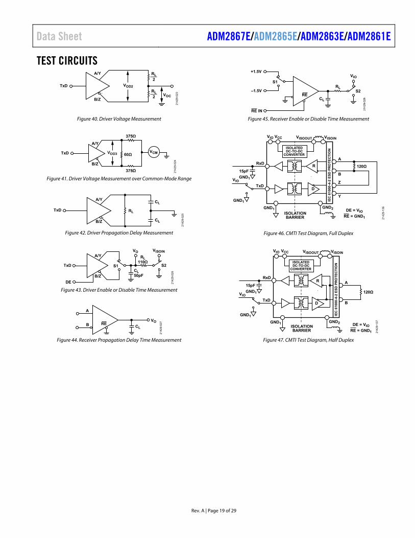
TEST CIRCUITS
VOD2
A/Y
B/Z
TxD
RL2
VOCRL2
2142
9-02
3
Figure 40. Driver Voltage Measurement
CM
2142
9-02
4
TxD
B/Z
A/Y
Figure 41. Driver Voltage Measurement over Common-Mode Range
2142
9-02
5
B/Z
A/Y
Figure 42. Driver Propagation Delay Measurement
RL110Ω
VISOIN
S2
VO
DE
TxD S1
B/Z
A/Y
CL50pF
2142
9-02
6
Figure 43. Driver Enable or Disable Time Measurement
REB
A
CL
VO
2142
9-02
7
Figure 44. Receiver Propagation Delay Time Measurement
RE
RL
VIO
S2
S1
+1.5V
–1.5V
RE IN
Figure 45. Receiver Enable or Disable Time Measurement
VCCVIO VISOOUT VISOIN
RxDA
B
R
TxDVIO
15pF
Z
Y
D
IEC
6100
0-4-
2 ES
D PR
OTE
CTIO
N
D
GND1
GND1
GND1
GND2 DE = VIORE = GND1
ISOLATIONBARRIER
120Ω
ISOLATEDDC-TO-DC
CONVERTER
2142
9-13
6
Figure 46. CMTI Test Diagram, Full Duplex
VCCVIO VISOOUT VISOIN
RxDA
B
R
TxDVIO
15pF
DD
GND1
GND1
GND1
GND2 DE = VIORE = GND1
ISOLATIONBARRIER
120Ω
ISOLATEDDC-TO-DC
CONVERTER
2142
9-13
7
IEC
6100
0-4-
2 ES
D PR
OTE
CTIO
NFigure 47. CMTI Test Diagram, Half Duplex

ADM2867E/ADM2865E/ADM2863E/ADM2861E Data Sheet
Rev. A | Page 20 of 29
THEORY OF OPERATION LOW EMI INTEGRATED DC-TO-DC CONVERTER The ADM2861E/ADM2863E/ADM2865E/ADM2867E include a flexible integrated dc-to-dc converter optimized for low radiated emissions (EMI). The isolated dc-to-dc converter is constructed of a set of chip scale coplanar coils separated by an insulating material. By exciting the upper coil with an ac signal, power is magnetically coupled across the isolation barrier where it is rectified and regulated. Because no direct electrical connection exists between the top and bottom coil, the primary and secondary side of the device remain galvanically isolated.
This isolated dc-to-dc converter features a regulated output of either 3.3 V or 5 V, selectable via the VSEL logic pin, which allows the user to optimize the supply rail of the RS-485 transceiver. For lower power applications, a 3.3 V supply can be chosen. For applications requiring a large differential output voltage, such as PROFIBUS®, the isolated dc-to-dc converter can be operated with a 5 V output. Table 14 shows the supported supply configurations for the isolated dc-to-dc converter.
Table 14. Isolated DC-to-DC Converter Supply Configuration
VSEL Pin VISO Output Supply Voltage
Supported VCC Supply Range
Connected to GNDISO 3.3 V 3 V to 5.5 V Connected to VISOOUT 5 V 4.5 V to 5.5 V
The integrated dc-to-dc converter is optimized to minimize radiated EMI, and allows designers to meet the CISPR32 and EN 55032 Class B requirements on a 2-layer PCB with the addition of two low cost, surface-mount device (SMD) ferrites. Follow layout recommendations during PCB design to minimize these emissions. See the PCB Layout and Electromagnetic Interference (EMI) section for more details.
80
70
60
50
40
30
20
10
0
RADI
ATED
FIE
LD S
TREN
GTH
(dBµ
V/m
)
30 100FREQUENCY (MHz)
1000
CLASS B
CLASS A
2142
9-03
5
Figure 48. Low Radiated Emissions DC-to-DC Converter Meets EN55022
Class B with Margin on a 2-Layer PCB
ROBUST LOW POWER DIGITAL ISOLATOR The ADM2861E/ADM2863E/ADM2865E/ADM2867E feature a low power digital isolator to galvanically isolate the primary and secondary side of the device. The use of coplanar transformer coils with an on and off keying modulation scheme allows high data throughput across the isolation barrier while minimizing radiation emissions. This architecture provides a robust digital isolator with immunity to common-mode transients of greater than 250 kV/µs across the full temperature and supply range of the device.
2
1
3
CHANNEL 2 (VCM)
CH1 2.0V 100ns/DIVCH3 2.0V
CH2 1kV
2142
9-11
3
CHANNEL 3 (RxD)
CHANNEL 1 (TxD)
Figure 49. Switching Correctly in the Presence of >250 kV/µs
Common-Mode Transients
HIGH DRIVER DIFFERENTIAL OUTPUT VOLTAGE The ADM2861E/ADM2863E/ADM2865E/ADM2867E feature a proprietary transmitter architecture with a low driver output impedance, resulting in an increased driver differential output voltage. This architecture is particularly useful when operating the device over long cable runs, where the dc resistance of the transmission line dominates signal attenuation. In these applications, the increased differential voltage improves noise margin and allows transmission over longer cable lengths. In addition, when operated as a 5 V transceiver (VSEL = VISO), the ADM2861E/ADM2863E/ADM2865E/ADM2867E meet or exceed the PROFIBUS requirement of a minimum 2.1 V differential output voltage.
IEC61000-4-2 ESD PROTECTION ESD is the sudden transfer of electrostatic charge between bodies at different potentials caused by near contact or induced by an electric field. ESD has the characteristics of high current in a short time period. The primary purpose of the IEC 61000-4-2 test is to determine the immunity of systems to external ESD events outside the system during operation. IEC 61000-4-2 describes testing using two coupling methods: contact discharge and air discharge. Contact discharge implies a direct contact between the discharge gun and the equipment under test (EUT). During air discharge testing, the charged electrode of the discharge gun is moved toward the EUT until a discharge occurs as an arc across the air gap. The discharge gun does not

Data Sheet ADM2867E/ADM2865E/ADM2863E/ADM2861E
Rev. A | Page 21 of 29
make direct contact with the EUT. A number of factors affect the results and repeatability of the air discharge test, including humidity, temperature, barometric pressure, distance, and rate of approach to the EUT. Air discharge testing is a more accurate representation of an actual ESD event than contact discharge but is not as repeatable. Therefore, contact discharge is the preferred test method. During testing, the data port is subjected to at least 10 positive and 10 negative single discharges. Selection of the test voltage is dependent on the system end environment. Figure 50 shows the 8 kV contact discharge current waveform as described in the IEC 61000-4-2 specification. Some of the key waveform parameters are rise times of less than 1 ns and pulse widths of approximately 60 ns.
tR = 0.7ns TO 1ns
IPEAK
I30ns
I60ns
30A90%
16A
8A
10%
30ns 60ns TIME
2142
9-03
6
Figure 50. IEC61000-4-2 ESD Waveform (8 kV)
Figure 51 shows the 8 kV contact discharge current waveform from the IEC 61000-4-2 standard compared to the HBM ESD 8 kV waveform. Figure 51 shows that the two standards specify a different waveform shape and peak current (IPEAK). The peak current associated with an IEC 61000-4-2 8 kV pulse is 30 A, whereas the corresponding peak current for HBM ESD is more than five times less, at 5.33 A. The other difference is the rise time of the initial voltage spike, with the IEC 61000-4-2 ESD waveform having a much faster rise time of 1 ns, compared to the 10 ns associated with the HBM ESD waveform. The amount of power associated with an IEC ESD waveform is much greater than that of an HBM ESD waveform. The HBM ESD standard requires the EUT to be subjected to three positive and three negative discharges, whereas in comparison, the IEC ESD standard requires 10 positive and 10 negative discharge tests.
The ADM2861E/ADM2863E/ADM2865E/ADM2867E are rated to ±12 kV contact and ±15 kV air ESD protection to the IEC61000-4-2 standard between the RS-485 bus pins (A, B, Y and Z) and GND2. The isolation barrier provides ±8 kV contact protection between the bus pins and GND1. These devices with IEC 61000-4-2 ESD ratings are better suited for operation in harsh environments when compared to other RS-485 transceivers that state varying levels of HBM ESD protection.
IPEAK
I30ns
I60ns
30A90%
16AIEC 61000-4-2 ESD 8kV
HBM ESD 8kV8A
5.33A
10%
tR = 0.7ns TO 1ns
30ns10ns 60ns TIME
2142
9-03
8
Figure 51. IEC61000-4-2 ESD8 kV Waveform Compared to HBM ESD 8 kV
Waveform
TRUTH TABLES Table 16 and Table 17 use the abbreviations shown in Table 15. VIO supplies the DE, TxD, RE, RxD, INVR, and INVD pins only.
Table 15. Truth Table Abbreviations Letter Description H High level I Indeterminate L Low level X Any state Z High impedance (off )
Table 16. Transmitting Truth Table Supply Status Inputs Outputs
VCC VIO DE TxD INVD Y Z On On H H L H L On On H H H L H On On H L L L H On On H L H H L On On L X X Z Z On Off X X X Z Z Off X X X X Z Z
Table 17. Receiving Truth Table Supply Status Inputs Output
VCC VIO A − B INVR RE RxD On On ≥−0.03 V L L H On On ≤0.03 V H L H On On ≤−0.2 V L L L On On ≥0.2 V H L L On On −0.2 V < A – B < −0.03 V L L I On On 0.03 V < A – B < 0.2 V H L I On On Inputs open/shorted X L H X On X X H Z X Off X X X I Off On X X L I

ADM2867E/ADM2865E/ADM2863E/ADM2861E Data Sheet
Rev. A | Page 22 of 29
RECEIVER FAIL-SAFE The ADM2861E/ADM2863E/ADM2865E/ADM2867E guarantee a logic high receiver output when the receiver inputs are shorted, open, or connected to a terminated transmission line with all drivers disabled. When the receiver inversion feature is disabled (INV/INVR = 0 V), a fail-safe logic high output is achieved by setting the receiver input threshold between −30 mV and −200 mV. If the differential receiver input voltage (A − B) is greater than or equal to −30 mV, the RxD pin is logic high. If the A − B input is less than or equal to −200 mV, RxD is logic low. Fail-safe is preserved when the receiver inversion feature is enabled (INVR = VIO) by setting the inverted receiver input threshold between 30 mV and 200 mV. In the case of a shorted or terminated bus with all transmitters disabled, the receiver differential input voltage is pulled to 0 V by the termination resistor, resulting in a logic high with a 30 mV minimum noise margin. This feature eliminates the need for external biasing components usually required to implement fail-safe.
These features are fully compatible with external fail-safe biasing configurations, which can be used in applications with legacy devices that lack fail-safe support, or in applications where additional noise margin is desired. See the AN-960 Application Note, RS-485/RS-422 Circuit Implementation Guide, for details on external fail-safe biasing.
DRIVER AND RECEIVER CABLE INVERSION The ADM2861E/ADM2863E/ADM2865E/ADM2867E feature cable inversion functionality to correct errors during installa-tion. This adjustment can be implemented in software on the controller driving the RS485 transceiver and helps avoid additional installation costs to fix wiring errors. The ADM2863E/ ADM2867E feature separate digital logic pins, INVD and INVR, to correct cases where the driver, receiver, or both are wired in reverse. Use the INVD pin to correct driver functionality when Y and Z are wired with the incorrect polarity. Use the INVR pin
to correct receiver functionality when A and B are wired with the incorrect polarity. The ADM2861E/ADM2865E are half-duplex devices that have a single inversion pin, INV, to correct both transmitter and receiver polarity. When the receiver is inverted, the device maintains a Logic 1 receiver output with a 30 mV noise margin when inputs are shorted together or open circuit. Figure 52 shows the receiver output in both inverted and noninverted cases.
+30mV
PHASE INVERTED RS-485INVR = H
RS-485INVR = L
+200mV
–30mV
–200mV
A – B
FAIL SAFE
FAIL SAFE
0
IN
1
1
0
2142
9-03
9
Figure 52. RS-485 and Phase Inverted RS-485 Comparison
HOT SWAP INPUTS When a circuit board is inserted in a powered (or hot) backplane, parasitic coupling from supply and ground rails to digital inputs may occur. The ADM2861E/ADM2863E/ ADM2865E/ADM2867E contain circuitry to ensure that the Y and Z outputs remain in a high impedance state during power-up, and then default to the correct states. For example, when VIO and VCC power up at the same time and the RE pin is pulled low, with the DE and TxD pins pulled high, the Y and Z outputs remain in high impedance until settling at an expected default high state for the Y pin and expected default low state for the Z pin.
Table 18. Product Description Table
Device Isolation Withstand Duplex
Maximum Data Rate Cable Inversion Feature Package(s) Available
ADM2861E 5.7 kV Half 500 kbps1 Inversion pin (INV) 28-lead SOIC_W with finer pitch ADM2863E 5.7 kV Full 500 kbps1 Separate driver (INVD) and receiver (INVR) inversion 28-lead SOIC_W with finer pitch ADM2865E 5.7 kV Half 25 Mbps Inversion pin (INV) 28-lead SOIC_W with finer pitch ADM2867E 5.7 kV Full 25 Mbps Separate driver (INVD) and receiver (INVR) inversion 28-lead SOIC_W with finer pitch 1 Driver outputs are slew rate limited to minimize common-mode emissions over long cable runs.

Data Sheet ADM2867E/ADM2865E/ADM2863E/ADM2861E
Rev. A | Page 23 of 29
196 TRANSCEIVERS ON THE BUS The standard RS-485 receiver input impedance is 12 kΩ (1 unit load), and the standard driver can drive up to 32 unit loads. The ADM2861E/ADM2863E/ADM2865E/ADM2867E transceiver has a 1/6 unit load receiver input resistance (equivalent to 72 kΩ), allowing up to 196 transceivers to be connected in parallel on one communication line. Any combination of these devices and other RS-485 transceivers with a total of 32 unit loads or fewer can be connected to the line.
DRIVER OUTPUT PROTECTION The ADM2861E/ADM2863E/ADM2865E/ADM2867E feature two methods to prevent excessive output current and power dissipation caused by faults or by bus contention. Current-limit protection on the output stage provides immediate protection against short circuits over the entire common-mode voltage range. In addition, a thermal shutdown circuit forces the driver outputs to a high impedance state if the die temperature rises excessively. This circuitry is designed to disable the driver outputs when a die temperature greater than 150°C is reached. As the device cools, the drivers are reenabled at a temperature of 140°C.
1.7 V TO 5.5 V VIO LOGIC SUPPLY The ADM2861E/ADM2863E/ADM2865E/ADM2867E feature a VIO logic supply pin to allow a flexible digital interface operational to voltages as low as 1.7 V. The VIO pin powers the primary side of the signal isolation, the logic inputs, and the RxD output. These input and output pins interface with logic devices such as universal asynchronous receiver/transmitters (UARTs), application specific integrated circuits (ASICs), and microcontrollers. For applications where these devices use I/Os operating at voltages other than the ADM2861E/ADM2863E/ ADM2865E/ADM2867E VCC supply voltage, the VIO supply can be powered from the same supply rail as the logic device. The VIO supply accepts a supply voltage between 1.7 V and 5.5 V, allowing communication with 1.8 V, 2.5 V, 3.3 V, and 5 V devices.

ADM2867E/ADM2865E/ADM2863E/ADM2861E Data Sheet
Rev. A | Page 24 of 29
APPLICATIONS INFORMATION PCB LAYOUT AND ELECTROMAGNETIC INTERFERENCE (EMI) The ADM2861E/ADM2863E/ADM2865E/ADM2867E meet EN 55032 Class B/CISPR32 radiated emissions requirements. Two external surface-mount technology (SMT) ferrite beads are used to pass the Class B limits with margin. No additional mitigation techniques, such as stitching capacitance, are needed, allowing system designers to create a compliant design on a 2-layer PCB, without the need for complex and area intensive layouts.
The ADM2861E/ADM2863E/ADM2865E/ADM2867E feature an internal split paddle lead frame on the bus side. For optimal noise suppression, filter the VISOOUT signal (Pin 25) and GNDISO signal (Pin 24, Pin 26, and Pin 28) for high frequency currents before routing power to the RS-485 transceiver and other circuitry. Two SMT ferrite beads, L1 and L2, are recommended to achieve this filtering. The size of the VISOOUT and GNDISO net must also be kept to a minimum. See Figure 53 for the recommended PCB layout.
1
2
3
4
5
6
7
8
9
1011
12
1314
2827
26
25
24
23
22
21
20
19
18
17
16
15
GND1GND1
VCC
VIO
GND1
GND1
GND110µF
0.1µF
0.1µF
VSELGNDISOVISOOUT
GND2
VISOIN
GNDISO
RxDREDE
INVRGND1
INVDTxD
GND2AB
GND2GND2
YZ
GNDISOMETAL KEEP OUT
ADM2867ETOP VIEW
(Not to Scale)
0.1µF
10µFL1
L20.1µF
2142
9-04
0
Figure 53. Recommended PCB Layout
The isoPower® integrated dc-to-dc converter contains switching frequencies between 180 MHz and 400 MHz. To effectively filter these frequencies, the impedance of the ferrite bead is chosen to be about 2 kΩ between the 100 MHz and 1 GHz frequency range. Some recommended SMT ferrites are shown in Table 19. Although these ferrite beads are required to achieve compliance to EN 55032 Class B, they are not needed for system functionality. The ADM2861E/ADM2863E/ADM2865E/ ADM2867E have been fully characterized with the recommended BLM15HD182SN1 ferrite beads.
Table 19. Examples of Surface-Mount Ferrite Beads Manufacturer Device No. Murata Electronics BLM15HD182SN1 Taiyo Yuden BKH1005LM182-T
The ADM2861E/ADM2863E/ADM2865E/ADM2867E can dissipate over 500 mW of power when fully loaded. Because it is not possible to apply a heat sink to an isolation device, the devices primarily depend on heat dissipation to the PCB through the GNDx pins. If the devices are used at high ambient temperatures, provide a thermal path from the GNDx pins to the PCB ground plane. The use of a solid GND1 and GND2 plane is recommended. Implementing a low thermal impedance between the top ground layers and internal ground layers reduce the temperature inside the chip significantly.
DEVICE POWER-UP The integrated isoPower isolated dc-to-dc converter requires 10 ms to power up to the setpoint of 3.3 V or 5 V. During this start-up time, it is not recommended to assert the DE driver enable signal.
In applications where the isolated dc-to-dc converter is operated with a 3.3 V output voltage (VSEL pin connected to GNDISO), the VCC supply rail must be greater than 3.135 V during the power-up sequence. After the 10 ms power-up duration, the VCC supply rail can operate across the full 3 V to 5.5 V range.
MAXIMUM DATA RATE vs. AMBIENT TEMPERATURE Under a large current load or when operating at high frequency operation, self heating effects within the isoPower dc-to-dc converter can limit the maximum ambient temperature achievable while retaining a silicon junction temperature below 150°C. This internal power dissipation is related to application conditions such as supply voltage configuration, switching frequency, effective load on the RS-485 bus, and the amount of time the transceiver is in transmit mode. Thermal performance also depends on the PCB design and thermal characteristics of a system.
In applications with a fully loaded RS-485 bus (equivalent to 54 Ω bus resistance) operating with VISO = 5 V, it is recommended to keep the VCC input supply greater than 4.75 V. If this is not possible for the ADM2865E/ADM2867E, limit either the maximum ambient temperature to 85°C or the maximum operating data rate to 6 Mbps. If this is not possible for the ADM2861E/ADM2863E, limit the maximum ambient temperature to 85°C.

Data Sheet ADM2867E/ADM2865E/ADM2863E/ADM2861E
Rev. A | Page 25 of 29
ISOLATED PROFIBUS SOLUTION The ADM2865E features a driver that is well suited for meeting the requirements of an isolated PROFIBUS node. When operating the ADM2865E as a PROFIBUS transceiver, connect the VSEL pin to the VISOOUT pin to operate the transceiver with a 5 V isolated supply voltage. The ADM2865E features the following characteris-tics that make it ideally suited for use in PROFIBUS applications:
• 5 V isolated transceiver power supply. The 5 V VISO output supply provides the required current for the RS-485 transceiver at up to 12 Mbps and the additional 5 mA required for the PROFIBUS termination network.
• The output driver meets or exceeds the PROFIBUS differential output requirements. To ensure the transmitter differential output does not exceed 7 V p-p over all conditions, place 10 Ω resistors in series with the A and B transmitter outputs.
• High speed timing to operate at 12 Mbps with low propagation delay and less than 10% transmitter and receiver skew.
• Low bus pin capacitance of 28 pF. • Class I (no loss of data) immunity to IEC 61000-4-4 EFT to
±1 kV can be achieved using a PROFIBUS shielded cable. At data rates of ≤500 kbps, IEC 61000-4-4 Class I to ±3 kV can be achieved with the addition of a 470 pF capacitor to GND1 on the RxD output pin.
EMC, EFT, AND SURGE In applications where additional levels of protection against IEC61000-4-4 EFT or IEC61000-4-5 surge events are required, external protection circuits can be added to further enhance the EMC robustness of these devices. See Figure 54 for a recom-mended protection circuit, which uses a series of SM712 transient voltage suppressor (TVS) and 10 Ω pulse proof resistors to achieve in excess of Level 4 IEC61000-4-2 ESD and IEC61000-4-4 EFT protection, and Level 2 IEC61000-4-5 surge protection. Table 20 and Table 21 describe the recommended components for protection and the protection levels.
VCC VIO
RxD
A
B
R
TxDZ
Y
D
IEC
6100
0-4-
2 ES
D PR
OTE
CTIO
N
D
SM712TVS
SM712TVS
10Ω
10Ω
GND1 GND2ISOLATIONBARRIER
10Ω
10Ω
120Ω
2142
9-04
1
Figure 54. Isolated RS-485 Solution with ESD, EFT, and Surge Protection
Table 20. Recommended Components for ESD, EFT, and Surge Protection Recommended Components Part Number TVS CDSOT23-SM712 10 Ω Pulse Proof Resistors CRCW060310R0FKEAHP
Table 21. Protection Levels with Recommended Circuit EMC Standard Protection Level (kV) ESD—Contact (IEC61000-4-2) ≥±30 (exceeds Level 4) ESD—Air (IEC61000-4-2) ≥±30 (exceeds Level 4) EFT (IEC61000-4-4) ≥±4 (exceeds Level 4) Surge (IEC61000-4-5) ≥±1 (Level 2)
INSULATION LIFETIME All insulation structures eventually break down when subjected to voltage stress over a sufficiently long period of time. The rate of insulation degradation is dependent on the characteristics of the voltage waveform applied across the insulation, as well as on the materials and material interfaces.
The two types of insulation degradation of primary interest are breakdown along surfaces exposed to the air and insulation wear out. Surface breakdown is the phenomenon of surface tracking and is the primary determinant of surface creepage requirements in system level standards. Insulation wear out is the phenomenon where charge injection or displacement currents inside the insulation material cause long-term insulation degradation.
Surface Tracking
Surface tracking is addressed in electrical safety standards by setting a minimum surface creepage based on the working voltage, the environmental conditions, and the properties of the insulation material. Safety agencies perform characterization testing on the surface insulation of components, allowing the components to be categorized in different material groups. Lower material group ratings are more resistant to surface tracking and can therefore provide adequate lifetime with smaller creepage. The minimum creepage for a given working voltage and material group is in each system level standard and is based on the total rms voltage across the isolation, pollution degree, and material group. See Table 6 for the material group and creepage information for the ADM2861E/ADM2863E/ ADM2865E/ADM2867E isolated RS-485 transceiver.
Insulation Wear Out
The lifetime of insulation caused by wear out is determined by the thickness, material properties, and the voltage stress applied across the insulation. It is important to verify that the product lifetime is adequate at the application working voltage. The working voltage supported by an isolator for wear out may not be the same as the working voltage supported for tracking. The working voltage applicable to tracking is specified in most standards.

ADM2867E/ADM2865E/ADM2863E/ADM2861E Data Sheet
Rev. A | Page 26 of 29
Testing and modeling show that the primary driver of long-term degradation is displacement current in the polyimide insulation, causing incremental damage. The stress on the insulation can be divided into broad categories, such as dc stress and ac component time varying voltage stress. DC stress causes little wear out because there is no displacement current, whereas ac component time varying voltage stress causes wear out.
The ratings in certification documents are typically based on 60 Hz sinusoidal stress to reflect isolation from the line voltage. However, many practical applications have combinations of 60 Hz ac and dc across the barrier, as shown in Equation 1. Because only the ac portion of the stress causes wear out, the equation can be rearranged to solve for the ac rms voltage, as shown in Equation 2. For insulation wear out with the polyimide materials used in these products, the ac rms voltage determines the product lifetime.
22DCRMSACRMS VVV += (1)
or
22DCRMSRMSAC VVV −= (2)
where: VRMS is the total rms working voltage. VAC RMS is the time varying portion of the working voltage. VDC is the dc offset of the working voltage.
Calculation and Use of Parameters Example
The following example frequently arises in power conversion applications. Assume that the line voltage on one side of the isolation is 240 V ac rms and a 400 V dc bus voltage is present on the other side of the isolation barrier. The isolator material is polyimide. To establish the critical voltages in determining the creepage, clearance, and lifetime of a device, see Figure 55 and the following equations.
ISO
LATI
ON
VOLT
AGE
TIME
VAC RMS
VRMS VDCVPEAK
2142
9-04
2
Figure 55. Critical Voltage Example
The working voltage across the barrier from Equation 1 is
22DCRMSACRMS VVV +=
22 400240 +=RMSV
VRMS = 466 V
This VRMS value is the working voltage used together with the material group and pollution degree when determining the creepage required by a system standard.
To determine if the lifetime is adequate, obtain the time varying portion of the working voltage. To obtain the ac rms voltage, use Equation 2.
22DCRMSRMSAC VVV −=
22 400466 −=RMSACV
VAC RMS = 240 V rms
In this case, the ac rms voltage is simply the line voltage of 240 V rms. This calculation is more relevant when the waveform is not sinusoidal. The value is compared to the limits for working voltage in Table 10 for the expected lifetime, which is less than a 60 Hz sine wave, and it is well within the limit for a 50-year service life.
The dc working voltage limit is set by the creepage of the package, as specified in IEC 60664-1. This value can differ for specific system level standards.
TYPICAL APPLICATIONS An example circuit using the ADM2867E as a full duplex RS-485 node is shown in Figure 56. Placement of the termina-tion resistor, RT, is dependent on the location of the node and the network topology. Refer to the AN-960 Application Note, RS-485/RS-422 Circuit Implementation Guide, for guidance on termination. Up to 192 transceivers can be connected to the bus. To minimize reflections, terminate the line at the receiving end in its characteristic impedance and keep stub lengths off the main line as short as possible. For half-duplex operation, this means that both ends of the line must be terminated because either end can be the receiving end.

Data Sheet ADM2867E/ADM2865E/ADM2863E/ADM2861E
Rev. A | Page 27 of 29
5V POWERSUPPLY
RxD
TxD
INVD
RE
VCC
MICROCONTROLLERAND
UART
RT
100nF
10uF 100nF
100nF 10µF 100nF
ADM2867E
VCC
ISOLATIONBARRIER
GNDISO
DECODE
ENCODE
ENCODE
REGULATOR
A
B
R
ENCODE
VIO
VISOIN
Z
Y
VISOOUTVSEL
D
ENCODE DECODE
IEC
6100
0-4-
2 ES
D PR
OTE
CTIO
N
RS-485 TRANSCEIVER
CABLEINVERT
GND2
DECODE
DECODE
INVR
DE
GND1GND1
LOW VOLTAGE1.8V/2.5V SUPPLY
GNDISO
LOW RADIATED EMISSIONS DC-TO-DC
DIGITAL ISOLATION iCoupler
RECTIFIEROSCILLATOR
2142
9-04
3
5V ISOLATED POWER
Figure 56. Example Circuit Diagram Using the ADM2867E

ADM2867E/ADM2865E/ADM2863E/ADM2861E Data Sheet
Rev. A | Page 28 of 29
OUTLINE DIMENSIONS
28 15
141
SEATINGPLANE
0.250.10
0.400.25
0.65 BSC
1.40REFCOPLANARITY
0.10
2.402.25
2.652.35
0.750.25
10.4510.15
7.607.40
10.5510.05
PKG
-004
678
06-0
1-20
15-A
× 45°
TOP VIEW
SIDE VIEW END VIEW0.320.23
1.270.40
8°0°
0.25 BSC(GAUGE PLANE)
PIN 1INDICATOR
Figure 57. 28-Lead Standard Small Outline, Wide Body, with Finer Pitch [SOIC_W_FP]
(RN-28-1) Dimensions shown in millimeters
ORDERING GUIDE Model1 Isolation (kV) Data Rate (Mbps) Duplex Temperature Range Package Description Package Option ADM2861EBRNZ 5.7 kV 0.5 Half −40°C to +105°C 28-Lead SOIC_W_FP RN-28-1 ADM2861EBRNZ-RL7 5.7 kV 0.5 Half −40°C to +105°C 28-Lead SOIC_W_FP RN-28-1 ADM2863EBRNZ 5.7 kV 0.5 Full −40°C to +105°C 28-Lead SOIC_W_FP RN-28-1 ADM2863EBRNZ-RL7 5.7 kV 0.5 Full −40°C to +105°C 28-Lead SOIC_W_FP RN-28-1 ADM2867EBRNZ 5.7 25 Full −40°C to +105°C 28-Lead SOIC_W_FP RN-28-1 ADM2867EBRNZ-RL7 5.7 25 Full −40°C to +105°C 28-Lead SOIC_W_FP RN-28-1 EVAL-ADM2861EEBZ Half Duplex Evaluation Board EVAL-ADM2863EEBZ Full Duplex Evaluation Board EVAL-ADM2867EEBZ Full Duplex Evaluation Board 1 Z = RoHS Compliant Part.

Data Sheet ADM2867E/ADM2865E/ADM2863E/ADM2861E
Rev. A | Page 29 of 29
PENDING PRODUCTS Table 22 lists the device within this isolated RS-485 transceiver family that is in development. Customers interested in samples of this new product or who want to be informed as soon as the released product is available can contact their local Analog Devices, Inc., sales representative. The following pending
product is a 5.7 kV rms isolated transceiver that includes an integrated isolated dc-to-dc converter. The device operates at the −40°C to +105°C temperature range and is packaged in a 28-lead, wide-body SOIC with finer pitch. High speed and slew rate limited versions are available in a half-duplex configuration.
Table 22. Pending Products
Model1 Isolation Data Rate (Mbps) Duplex Temperature Range Package Description
Package Option
ADM2865EBRNZ 5.7 kV 25 Half −40°C to +105°C 28-Lead SOIC_W_FP RN-28-1 ADM2865EBRNZ-RL7 5.7 kV 25 Half −40°C to +105°C 28-Lead SOIC_W_FP RN-28-1 EVAL-ADM2865EEBZ Half Duplex Evaluation Board 1 Z = RoHS Compliant Part.
©2020 Analog Devices, Inc. All rights reserved. Trademarks and registered trademarks are the property of their respective owners. D21429-6/20(A)