5v, 500ma low drop voltage regulator - s · pdf filereset circuit sensing of output voltage...
TRANSCRIPT

This is information on a product in full production.
September 2013 Doc ID 13103 Rev 14 1/35
1
L4995
5V, 500mA low drop voltage regulator
Datasheet − production data
Features
■ Operating DC supply voltage range 5.6V to 31V
■ Low dropout voltage
■ Low quiescent current consumption
■ Reset circuit sensing of output voltage down to 1 V
■ Programmable reset pulse delay with external capacitor
■ Programmable watchdog(a) timer with external capacitor
■ Thermal shutdown and short circuit protection
■ Wide temperature range (Tj = -40 °C to 150 °C)
■ Enable(a) input for enabling/disabling the voltage regulator
DescriptionL4995 is a family of monolithic integrated 5 V voltage regulators with a low drop voltage at currents of up to 500 mA, available in both 12 and 24 pin packages.
The output voltage regulating element consists of a p-channel MOS and regulation is performed regardless of input voltage transients of up to 40V.
The high precision of the output voltage is obtained using a pre-trimmed reference voltage. The L4995 family is protected against short circuit and overtemperature protection switches off the devices in the case of extremely high power dissipation. The L4995 integrates the watchdog, enable and externally programmable reset circuits. The L4995A features the externally programmable reset and enable. Finally the L4995R features the externally programmable reset.
The combination of such features makes this device particularly flexible and suitable to supply microprocessor systems in automotive applications.
Max DC supply voltage VS 40V
Max output voltage tolerance ΔV0 +/-2%
Max dropout voltage Vdp 500mV
Output current I0 500mA
Quiescent current Iqn 3µA(1)
1. Typical value with regulator disabled
a. Watchdog and Enable facilities are available according to Device summary table.
PowerSSO-12 PowerSSO-24
Table 1. Device summary
PackageOrder codes
Tube Tape and reel
PowerSSO-12 (exposed pad) L4995J - L4995AJ - L4995RJ L4995JTR - L4995AJTR - L4995RJTR
PowerSSO-24 (exposed pad) L4995K - L4995AK - L4995RK L4995KTR - L4995AKTR - L4995RKTR
P/N Watchdog Reset Enable
L4995J - L4995K X X X
L4995AJ - L4995AK - X X
L4995RJ - L4995RK - X -
www.st.com

Contents L4995
2/35 Doc ID 13103 Rev 14
Contents
1 Block diagrams and pins descriptions . . . . . . . . . . . . . . . . . . . . . . . . . . 5
2 Electrical specifications . . . . . . . . . . . . . . . . . . . . . . . . . . . . . . . . . . . . . . 8
2.1 Absolute maximum ratings . . . . . . . . . . . . . . . . . . . . . . . . . . . . . . . . . . . . . 8
2.2 Thermal data . . . . . . . . . . . . . . . . . . . . . . . . . . . . . . . . . . . . . . . . . . . . . . . 9
2.3 Electrical characteristics . . . . . . . . . . . . . . . . . . . . . . . . . . . . . . . . . . . . . . . 9
2.4 Electrical characteristics curves . . . . . . . . . . . . . . . . . . . . . . . . . . . . . . . . 12
2.5 Test circuit and waveforms plot . . . . . . . . . . . . . . . . . . . . . . . . . . . . . . . . 15
2.5.1 Load regulation . . . . . . . . . . . . . . . . . . . . . . . . . . . . . . . . . . . . . . . . . . . 15
3 Application information . . . . . . . . . . . . . . . . . . . . . . . . . . . . . . . . . . . . . 17
3.1 Voltage regulator . . . . . . . . . . . . . . . . . . . . . . . . . . . . . . . . . . . . . . . . . . . 18
3.2 Reset . . . . . . . . . . . . . . . . . . . . . . . . . . . . . . . . . . . . . . . . . . . . . . . . . . . . 18
3.3 Watchdog . . . . . . . . . . . . . . . . . . . . . . . . . . . . . . . . . . . . . . . . . . . . . . . . . 19
4 Package and PCB thermal data . . . . . . . . . . . . . . . . . . . . . . . . . . . . . . . 20
4.1 PowerSSO-12 thermal data . . . . . . . . . . . . . . . . . . . . . . . . . . . . . . . . . . . 20
4.2 PowerSSO-24 thermal data . . . . . . . . . . . . . . . . . . . . . . . . . . . . . . . . . . . 23
5 Package and packing information . . . . . . . . . . . . . . . . . . . . . . . . . . . . . 26
5.1 ECOPACK® . . . . . . . . . . . . . . . . . . . . . . . . . . . . . . . . . . . . . . . . . . . . . . . 26
5.2 PowerSSO-24 mechanical data . . . . . . . . . . . . . . . . . . . . . . . . . . . . . . . . 28
5.3 PowerSSO-12 packing information . . . . . . . . . . . . . . . . . . . . . . . . . . . . . 30
5.4 PowerSSO-24 packing information . . . . . . . . . . . . . . . . . . . . . . . . . . . . . 31
6 Revision history . . . . . . . . . . . . . . . . . . . . . . . . . . . . . . . . . . . . . . . . . . . 32

L4995 List of tables
Doc ID 13103 Rev 14 3/35
List of tables
Table 1. Device summary . . . . . . . . . . . . . . . . . . . . . . . . . . . . . . . . . . . . . . . . . . . . . . . . . . . . . . . . . . 1Table 2. Pins descriptions. . . . . . . . . . . . . . . . . . . . . . . . . . . . . . . . . . . . . . . . . . . . . . . . . . . . . . . . . . 6Table 3. Absolute maximum ratings . . . . . . . . . . . . . . . . . . . . . . . . . . . . . . . . . . . . . . . . . . . . . . . . . . 8Table 4. Thermal data. . . . . . . . . . . . . . . . . . . . . . . . . . . . . . . . . . . . . . . . . . . . . . . . . . . . . . . . . . . . . 9Table 5. General . . . . . . . . . . . . . . . . . . . . . . . . . . . . . . . . . . . . . . . . . . . . . . . . . . . . . . . . . . . . . . . . . 9Table 6. Reset . . . . . . . . . . . . . . . . . . . . . . . . . . . . . . . . . . . . . . . . . . . . . . . . . . . . . . . . . . . . . . . . . 10Table 7. Watchdog . . . . . . . . . . . . . . . . . . . . . . . . . . . . . . . . . . . . . . . . . . . . . . . . . . . . . . . . . . . . . . 11Table 8. Enable. . . . . . . . . . . . . . . . . . . . . . . . . . . . . . . . . . . . . . . . . . . . . . . . . . . . . . . . . . . . . . . . . 11Table 9. PowerSSO-12 thermal parameter . . . . . . . . . . . . . . . . . . . . . . . . . . . . . . . . . . . . . . . . . . . 22Table 10. PowerSSO-24 thermal parameter . . . . . . . . . . . . . . . . . . . . . . . . . . . . . . . . . . . . . . . . . . . 25Table 11. PowerSSO-12 mechanical data . . . . . . . . . . . . . . . . . . . . . . . . . . . . . . . . . . . . . . . . . . . . . 27Table 12. PowerSSO-24 mechanical data . . . . . . . . . . . . . . . . . . . . . . . . . . . . . . . . . . . . . . . . . . . . . 29Table 13. Document revision history . . . . . . . . . . . . . . . . . . . . . . . . . . . . . . . . . . . . . . . . . . . . . . . . . 32

List of figures L4995
4/35 Doc ID 13103 Rev 14
List of figures
Figure 1. Block diagram of L4995 . . . . . . . . . . . . . . . . . . . . . . . . . . . . . . . . . . . . . . . . . . . . . . . . . . . . 5Figure 2. Block diagram of L4995A . . . . . . . . . . . . . . . . . . . . . . . . . . . . . . . . . . . . . . . . . . . . . . . . . . . 5Figure 3. Block diagram of L4995R . . . . . . . . . . . . . . . . . . . . . . . . . . . . . . . . . . . . . . . . . . . . . . . . . . . 6Figure 4. Pins configurations (L4995) . . . . . . . . . . . . . . . . . . . . . . . . . . . . . . . . . . . . . . . . . . . . . . . . . 7Figure 5. Output voltage vs Tj . . . . . . . . . . . . . . . . . . . . . . . . . . . . . . . . . . . . . . . . . . . . . . . . . . . . . . 12Figure 6. Output voltage vs VS. . . . . . . . . . . . . . . . . . . . . . . . . . . . . . . . . . . . . . . . . . . . . . . . . . . . . . 12Figure 7. Drop voltage vs output current . . . . . . . . . . . . . . . . . . . . . . . . . . . . . . . . . . . . . . . . . . . . . . 12Figure 8. Current consumption vs output current. . . . . . . . . . . . . . . . . . . . . . . . . . . . . . . . . . . . . . . . 12Figure 9. Current consumption vs input voltage . . . . . . . . . . . . . . . . . . . . . . . . . . . . . . . . . . . . . . . . 12Figure 10. Current limitation vs Tj . . . . . . . . . . . . . . . . . . . . . . . . . . . . . . . . . . . . . . . . . . . . . . . . . . . . 12Figure 11. Current limitation vs input voltage. . . . . . . . . . . . . . . . . . . . . . . . . . . . . . . . . . . . . . . . . . . . 13Figure 12. Short circuit current vs input voltage. . . . . . . . . . . . . . . . . . . . . . . . . . . . . . . . . . . . . . . . . . 13Figure 13. Output voltage vs enable voltage . . . . . . . . . . . . . . . . . . . . . . . . . . . . . . . . . . . . . . . . . . . . 13Figure 14. VEn_high vs Tj . . . . . . . . . . . . . . . . . . . . . . . . . . . . . . . . . . . . . . . . . . . . . . . . . . . . . . . . . . . 13Figure 15. VEN_LOW vs Tj . . . . . . . . . . . . . . . . . . . . . . . . . . . . . . . . . . . . . . . . . . . . . . . . . . . . . . . . . . . 13Figure 16. VRhth vs Tj . . . . . . . . . . . . . . . . . . . . . . . . . . . . . . . . . . . . . . . . . . . . . . . . . . . . . . . . . . . . . . 13Figure 17. VRlth vs Tj . . . . . . . . . . . . . . . . . . . . . . . . . . . . . . . . . . . . . . . . . . . . . . . . . . . . . . . . . . . . . . 14Figure 18. Vwhth vs Tj . . . . . . . . . . . . . . . . . . . . . . . . . . . . . . . . . . . . . . . . . . . . . . . . . . . . . . . . . . . . . . 14Figure 19. Vwlth vs Tj . . . . . . . . . . . . . . . . . . . . . . . . . . . . . . . . . . . . . . . . . . . . . . . . . . . . . . . . . . . . . . 14Figure 20. Icr and Icwc vs Tj . . . . . . . . . . . . . . . . . . . . . . . . . . . . . . . . . . . . . . . . . . . . . . . . . . . . . . . . . 14Figure 21. Idr and Icwd vs Tj . . . . . . . . . . . . . . . . . . . . . . . . . . . . . . . . . . . . . . . . . . . . . . . . . . . . . . . . . 14Figure 22. Twop vs Tj . . . . . . . . . . . . . . . . . . . . . . . . . . . . . . . . . . . . . . . . . . . . . . . . . . . . . . . . . . . . . . 14Figure 23. PSRR . . . . . . . . . . . . . . . . . . . . . . . . . . . . . . . . . . . . . . . . . . . . . . . . . . . . . . . . . . . . . . . . . 15Figure 24. Load regulation test circuit . . . . . . . . . . . . . . . . . . . . . . . . . . . . . . . . . . . . . . . . . . . . . . . . . 15Figure 25. Maximum load variation response . . . . . . . . . . . . . . . . . . . . . . . . . . . . . . . . . . . . . . . . . . . 16Figure 26. L4995 application schematic(1) . . . . . . . . . . . . . . . . . . . . . . . . . . . . . . . . . . . . . . . . . . . . . . 17Figure 27. Stability region(1). . . . . . . . . . . . . . . . . . . . . . . . . . . . . . . . . . . . . . . . . . . . . . . . . . . . . . . . . 17Figure 28. Behavior of output current versus regulated voltage Vo . . . . . . . . . . . . . . . . . . . . . . . . . . . 18Figure 29. Reset timing diagram . . . . . . . . . . . . . . . . . . . . . . . . . . . . . . . . . . . . . . . . . . . . . . . . . . . . . 19Figure 30. Watchdog timing diagram . . . . . . . . . . . . . . . . . . . . . . . . . . . . . . . . . . . . . . . . . . . . . . . . . . 19Figure 31. PowerSSO-12 PC board(1) . . . . . . . . . . . . . . . . . . . . . . . . . . . . . . . . . . . . . . . . . . . . . . . . . 20Figure 32. Rthj-amb vs PCB copper area in open box free air condition . . . . . . . . . . . . . . . . . . . . . . 20Figure 33. PowerSSO-12 thermal impedance junction ambient single pulse . . . . . . . . . . . . . . . . . . . 21Figure 34. Thermal fitting model of Vreg in PowerSSO-12 . . . . . . . . . . . . . . . . . . . . . . . . . . . . . . . . . 21Figure 35. PowerSSO-24 PC board(1) . . . . . . . . . . . . . . . . . . . . . . . . . . . . . . . . . . . . . . . . . . . . . . . . . 23Figure 36. Rthj-amb vs PCB copper area in open box free air condition . . . . . . . . . . . . . . . . . . . . . . 23Figure 37. PowerSSO-24 thermal impedance junction ambient single pulse . . . . . . . . . . . . . . . . . . . 24Figure 38. Thermal fitting model of Vreg in PowerSSO-24 . . . . . . . . . . . . . . . . . . . . . . . . . . . . . . . . . 24Figure 39. PowerSSO-12 package dimensions . . . . . . . . . . . . . . . . . . . . . . . . . . . . . . . . . . . . . . . . . . 26Figure 40. PowerSSO-24 package dimensions . . . . . . . . . . . . . . . . . . . . . . . . . . . . . . . . . . . . . . . . . . 28Figure 41. PowerSSO-12 tube shipment (no suffix) . . . . . . . . . . . . . . . . . . . . . . . . . . . . . . . . . . . . . . 30Figure 42. PowerSSO-12 tape and reel shipment (suffix “TR”) . . . . . . . . . . . . . . . . . . . . . . . . . . . . . . 30Figure 43. PowerSS0-24 tube shipment (no suffix) . . . . . . . . . . . . . . . . . . . . . . . . . . . . . . . . . . . . . . . 31Figure 44. PowerSSO-24 tape and reel shipment (suffix “TR”) . . . . . . . . . . . . . . . . . . . . . . . . . . . . . . 31

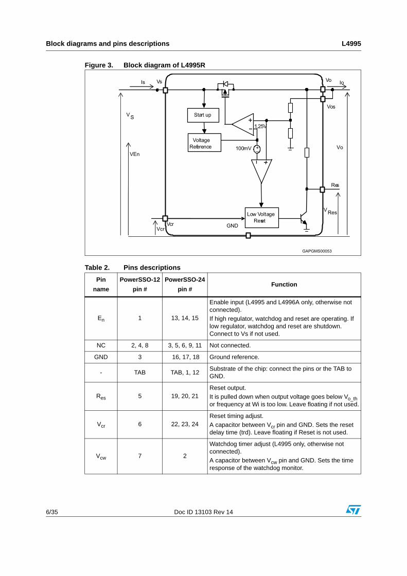
L4995 Block diagrams and pins descriptions
Doc ID 13103 Rev 14 5/35
1 Block diagrams and pins descriptions
Figure 1. Block diagram of L4995
Figure 2. Block diagram of L4995A
Block diagrams and pins descriptions L4995
6/35 Doc ID 13103 Rev 14
Figure 3. Block diagram of L4995R
Table 2. Pins descriptions
Pin
name
PowerSSO-12
pin #
PowerSSO-24
pin #Function
En 1 13, 14, 15
Enable input (L4995 and L4996A only, otherwise not connected).If high regulator, watchdog and reset are operating. If low regulator, watchdog and reset are shutdown. Connect to Vs if not used.
NC 2, 4, 8 3, 5, 6, 9, 11 Not connected.
GND 3 16, 17, 18 Ground reference.
- TAB TAB, 1, 12Substrate of the chip: connect the pins or the TAB to GND.
Res 5 19, 20, 21Reset output.It is pulled down when output voltage goes below Vo_th or frequency at Wi is too low. Leave floating if not used.
Vcr 6 22, 23, 24Reset timing adjust.A capacitor between Vcr pin and GND. Sets the reset delay time (trd). Leave floating if Reset is not used.
Vcw 7 2
Watchdog timer adjust (L4995 only, otherwise not connected).A capacitor between Vcw pin and GND. Sets the time response of the watchdog monitor.

L4995 Block diagrams and pins descriptions
Doc ID 13103 Rev 14 7/35
Figure 4. Pins configurations (L4995)
Wi 9 4Watchdog input (L4995 only, otherwise not connected).If the frequency at this input pin is too low, the Reset output is activated.
Vos 10 7 Regulator voltage output sensing.
Vo 11 85 voltage regulator output.Block to ground with a capacitor >100nF (needed for regulator stability).
VS 12 10Supply voltage.Block to ground directly at VS pin with a ceramic capacitor (e.g. 200nF).
Table 2. Pins descriptions (continued)
Pin
name
PowerSSO-12
pin #
PowerSSO-24
pin #Function

Electrical specifications L4995
8/35 Doc ID 13103 Rev 14
2 Electrical specifications
2.1 Absolute maximum ratingsStressing the device above the rating listed in the “Absolute maximum ratings” table may cause permanent damage to the device. These are stress ratings only and operation of the device at these or any other conditions above those indicated in the Operating sections of this specification is not implied. Exposure to Absolute Maximum Rating conditions for extended periods may affect device reliability. Refer also to the STMicroelectronics SURE Program and other relevant quality documents.
Table 3. Absolute maximum ratings
Symbol Parameter Value Unit
VVsdc DC supply voltage - 0.3 to 40 V
IVsdc Input current Internally limited
VVo(1)
1. Using the typical application schematic with Cout= 10 µF and Iout=0 A, when the regulator is switched-on, an overshoot exceeding 6 V could occur.This behavior does not impact the reliability of the regulator.
DC output voltage - 0.3 to 6 V
IVo DC output current Internally limited
VWi Watchdog input voltage -0.3 to VVo + 0.3 V
Vod Res output voltage -0.3 to VVo + 0.3 V
Iod Res output current Internally limited
Vcr Vcr voltage - 0.3 to VVo + 0.3 V
Vcw Watchdog delay voltage - 0.3 to VVo + 0.3 V
VEn Enable input - 0.3 to VVsdc +0.3 V
Tj Junction temperature - 40 to 150 C
VESD ESD voltage level (HBM-MIL STD 883C) ± 2 kV
VESD ESD voltage level (CDM AEC-Q100-011) 750 V

L4995 Electrical specifications
Doc ID 13103 Rev 14 9/35
2.2 Thermal dataFor details, please refer to Section 4.1: PowerSSO-12 thermal data and Section 4.2: PowerSSO-24 thermal data.
mm
2.3 Electrical characteristicsValues specified in this section are for Vs = 5.6V to 31V, Tj = -40 °C to +150 °C unless otherwise stated.
Table 4. Thermal data(1)
1. The values quoted are for PCB 77mm x 86mm x 1.6mm, FR4, double layer; Copper thickness 0.070mm Copper area 3cm2 Thermal Vias, Thermal vias separation 1.2 mm, Thermal via diameter 0.3 mm +/- 0.08 mm, Cu thickness on vias 0.025 mm.
Symbol Parameter Value Unit
Rthj-case
Thermal resistance Junction to Case:PowerSSO-12PowerSSO-24
54
°K/W°K/W
Rthj-amb
Thermal resistance Junction to Ambient:PowerSSO-12
PowerSSO-24
52
38
°K/W
°K/W
Table 5. General
Pin Symbol Parameter Test condition Min. Typ. Max. Unit
Vo Vo_ref Output voltageVS = 5.6 to 31VIo = 0 to 500mA
4.9 5.00 5.1 V
Vo Ishort Short circuit current VS = 13.5V (1) 550 800 1050 mA
Vo Ilim(2) Output current limitation VS = 13.5V (1) 600 900 1250 mA
VS, Vo Vline Line regulation voltageVS = 5.6 to 31VIo = 0 to 500mA
25 mV
Vo Vload Load regulation voltage Io = 0 to 500mA 25 mV
VS, Vo Vdp(3) Drop voltage Io = 400mA 270 500 mV
VS, Vo SVR Ripple rejection fr = 100 Hz (4) 55 dB
VS, Vo IqsCurrent consumption with regulator disabled
VS = 13.5V,
En = low3 10 µA
VS, Vo Iqn_1Current consumptionwith regulator enabled
VS = 13.5V, Io < 1mA,
90 160 µA
VS, Vo Iqn_50Current consumptionwith regulator enabled
VS = 13.5V,Io = 50mA,
290 400 µA

Electrical specifications L4995
10/35 Doc ID 13103 Rev 14
VS, Vo Iqn_150Current consumption
with regulator enabled
VS = 13.5V,
Io = 150mA,740 1000 µA
VS, Vo Iqn_250Current consumption
with regulator enabled
VS= 13.5V,
Io= 250mA,1 1.4 mA
VS, Vo Iqn_500Current consumptionwith regulator enabled
VS= 13.5V,Io= 500mA,
2.1 2.7 mA
TwThermal protection temperature
150 190 °C
Tw_hyThermal protection temperature hysteresis
10 °C
1. See Figure 28.
2. Measured output current when the output voltage has dropped 100mV from its nominal value obtained at Vs=13.5V and Io= 250mA.
3. Vs-Vo measured when the output voltage has dropped 100mV from its nominal value obtained at Vs=13.5V and Io= 250mA.
4. Guaranteed by design.
Table 6. Reset
Pin Symbol Parameter Test condition Min. Typ. Max. Unit
Res Vres_l Reset output low voltageRext = 5kΩ to Vo,Vo > 1V
0.4 V
Res IRes_lkgReset output high leakage current
VRes = 5V 1 µA
Res RResPull up internal resistance (versus Vo)
10 20 40 kΩ
Res Vo_thVo out of regulation threshold
VS = 5.6 to 31V
Io = 1 to 500mA6% 8% 10%
below Vo_ref
Vcr VRlthReset delay circuit low threshold
VS = 13.5V 10% 13% 16% Vo_ref
Vcr VRhthReset delay circuit high threshold
VS =13.5V 44% 47% 50% Vo_ref
Vcr Icr Charge current VS = 13.5V 8 15 30 µA
Vcr Idr Discharge current VS = 13.5V 8 15 30 µA
Res Trr Reset reaction time(1)
1. When Vo becomes lower than 4V, the reset reaction time decreases down to 2µs assuring a faster reset condition in this particular case.
Vo = Vo_th -100mV 100 250 700 µs
Res Trd Reset delay timeVS = 13.5V, Ctr = 47nF
12 33 73 ms
Table 5. General (continued)
Pin Symbol Parameter Test condition Min. Typ. Max. Unit

L4995 Electrical specifications
Doc ID 13103 Rev 14 11/35
Table 7. Watchdog
Pin Symbol Parameter Test condition Min. Typ. Max. Unit
Wi Vih Input high voltage VS = 13.5V 3.5 V
Wi Vil Input low voltage VS = 13.5V 1.5 V
Wi Vih Input hysteresis VS = 13.5V 500 mV
Wi Iwi Pull down currentVS = 13.5V Vwi = 3.5V
6 10 µA
Vcw Vwlth Low threshold VS = 13.5V 10% 13% 16% Vo_ref
Vcw Vwhth High threshold VS = 13.5V 44% 47% 50% Vo_ref
Vcw Icwc Charge currentVS = 13.5V,
Vcw = 0.1V5 10 20 µA
Vcw Icwd Discharge currentVS = 13.5V,
Vcw = 2.5V1.25 2.5 5 µA
Vcw Twop Watchdog period VS = 13.5V, Ctw = 47nF
20 40 80 ms
Res twol Watchdog output low timeVS = 13.5V, Ctw = 47nF
4 8 16 ms
Table 8. Enable
Pin Symbol Parameter Test condition Min. Typ. Max. Unit
En VEn_low En input low voltage 1 V
En VEn_high En input high voltage 3 V
En VEn_hyst En input hysteresis 830 mV
En IEn Pull down current VS = 13.5V 10 18 µA

Electrical specifications L4995
12/35 Doc ID 13103 Rev 14
2.4 Electrical characteristics curvesFigure 5. Output voltage vs Tj Figure 6. Output voltage vs VS
Figure 7. Drop voltage vs output current Figure 8. Current consumption vs output current
Figure 9. Current consumption vs input voltage
Figure 10. Current limitation vs Tj

L4995 Electrical specifications
Doc ID 13103 Rev 14 13/35
Figure 11. Current limitation vs input voltage Figure 12. Short circuit current vs input voltage
e
Figure 13. Output voltage vs enable voltage Figure 14. VEn_high vs Tj
Figure 15. VEN_LOW vs Tj Figure 16. VRhth vs Tj

Electrical specifications L4995
14/35 Doc ID 13103 Rev 14
Figure 17. VRlth vs Tj Figure 18. Vwhth vs Tj
Figure 19. Vwlth vs Tj Figure 20. Icr and Icwc vs Tj
Figure 21. Idr and Icwd vs Tj Figure 22. Twop vs Tj

L4995 Electrical specifications
Doc ID 13103 Rev 14 15/35
2.5 Test circuit and waveforms plot
2.5.1 Load regulation
Figure 24. Load regulation test circuit
Figure 23. PSRR
0,00
10,00
20,00
30,00
40,00
50,00
60,00
70,00
80,00
0,10 1,00 10,00 10100,00 1000,00 1000000,00
C0= 4.7 µF= 4.7 µF
GAPGMS00073FREQUENCY [KHz]
PSRR [dB]

Electrical specifications L4995
16/35 Doc ID 13103 Rev 14
Figure 25. Maximum load variation response
0,00E+00 5,00E-05 1,00E-04 1,50E-04 2,00E-04 2,50E-04 3,00E-04 3,50E-04 4,00E-04
Time [s]
V0 [1V / div]
I 0 [200mA / div]
GAPGMS00081

L4995 Application information
Doc ID 13103 Rev 14 17/35
3 Application information
Figure 26. L4995 application schematic(1)
1. The input capacitor Cs > 200nF is necessary for the smoothing of line disturbances. The output capacitor C01 > 100nF is necessary for the stability of the regulation loop. In order to dampen output voltage oscillations during high load current surges, it is recommended an additional electrolytic capacitor C02 > 10µF to be placed at the output pin.
Figure 27. Stability region(1)
1. The curve which describes the minimum ESR is derived from characterization data on the regulator with connected ceramic capacitors which feature low ESR values (at 100 kHz). Any capacitor with further lower ESR than the given plot value must be evaluated in each and every case.
0.001
0.01
0.1
1
10
100
0.5 5 10 15 20 25 30 35 40 45 50
Co (uF)
ES
R (
Oh
m)
ESR min
ESR max
Unstable region
Stability region
Undefined region

Application information L4995
18/35 Doc ID 13103 Rev 14
3.1 Voltage regulatorVoltage regulator uses a p-channel transistor as a regulating element. With this structure, very low dropout voltage at current up to 500mA is obtained. The output voltage is regulated up to transient input supply voltage of 40V. No functional interruption due to over-voltage pulses is generated. A short circuit protection to GND is provided.
The voltage regulator is active when En is high.
Figure 28. Behavior of output current versus regulated voltage Vo
3.2 ResetThe reset circuit supervises the output voltage Vo. The Vo_th reset threshold is defined with the in-ternal reference voltage and a resistor output divider. If the output voltage becomes lower than Vo_th then Res goes low with a reaction time trr. The reset low signal is guaranteed for an output voltage Vo greater than 1V.
When the output voltage becomes higher than Vo_th then Res goes high with a delay trd.This delay is obtained by an internal oscillator.
The oscillator period is given by:
Equation 1
Tosc = [(VRhth-VRlth) x Ctr] / Icr + [(VRhth-VRlth) x Ctr] / Idr
where:
Icr:is an internally generated charge current
Idr:is an internally generated discharge current
VRhth, VRlth:are two voltages defined with the output voltage and a resistor output divider
Ctr:is an external capacitance.
trd is given by:
Equation 2
trd = (VRhth x Ctr)/Icr + 3 x Tosc
Vo
Vo_ref
IoutIshort Ilim

L4995 Application information
Doc ID 13103 Rev 14 19/35
Reset is active when En is high.
Figure 29. Reset timing diagram
3.3 WatchdogA connected microcontroller is monitored by the watchdog input Wi. If pulses are missing, the Reset output pin is set to low. The pulse sequence time can be set within a wide range with the external capacitor, Ctw. The watchdog circuit discharges the capacitor Ctw, with the constant current Icwd. If the lower threshold Vwlth is reached, a watchdog reset is generated. To prevent this the microcontroller must generate a positive edge during the discharge of the capacitor before the voltage has reached the threshold Vwlth. In order to calculate the minimum time t, during which the micro-controller must output the positive edge, the following equation can be used:
Equation 3
(Vwhth-Vwlth) x Ctw = Icwd x t
Every Wi positive edge switches the current source from discharging to charging. The same happens when the lower threshold is reached. When the voltage reaches the upper threshold, Vwhth, the current switches from charging to discharging. The result is a saw-tooth voltage at the watchdog timer capacitor Ctw.
Figure 30. Watchdog timing diagram
trr
< trr
trd
ToscVrhth
Vrlth
Res
Vcr
Vo
Wi
Vout_th
trr
< trr
trd
ToscVrhth
Vrlth
Res
Vcr
Vo
Wi
Vout_th
GAPGMS00077

Package and PCB thermal data L4995
20/35 Doc ID 13103 Rev 14
4 Package and PCB thermal data
4.1 PowerSSO-12 thermal data
Figure 31. PowerSSO-12 PC board(1)
1. Layout condition of Rth and Zth measurements (PCB: Double layer, Thermal Vias, FR4 area= 77mm x 86mm,PCB thickness=1.6mm, Cu thickness=70μm (front and back side) Thermal vias separation 1.2 mm, Thermal via diameter 0.3 mm +/- 0.08 mm, Cu thickness on vias 0.025 mm, Footprint dimension 4.1 mm x 6.5 mm).
Figure 32. Rthj-amb vs PCB copper area in open box free air condition
40
45
50
55
60
65
70
0 2 4 6 8 10
RTHj_a_amb(°C/ W)
PCB Cu heaeat sink areaea ( cm^ 2)GAPGMS00082

L4995 Package and PCB thermal data
Doc ID 13103 Rev 14 21/35
Figure 33. PowerSSO-12 thermal impedance junction ambient single pulse
Equation 4: pulse calculation formula
where δ = tP/T
Figure 34. Thermal fitting model of Vreg in PowerSSO-12
0,1
1
10
100
0,0001 0,001 0,01 0,1 1 10 100 1000Time ( s)
ZTH (°C/ W)Footprint
8 cm2
2 cm2
ZTHδ RTH δ ZTHtp 1 δ–( )+⋅=

Package and PCB thermal data L4995
22/35 Doc ID 13103 Rev 14
Table 9. PowerSSO-12 thermal parameter
Area/island (cm2) Footprint 2 8
R1 (°C/W) 0.45
R2 (°C/W) 1.79
R3 (°C/W) 7
R4 (°C/W) 10 10 9
R5 (°C/W) 22 15 10
R6 (°C/W) 26 20 15
C1 (W.s/°C) 0.001
C2 (W.s/°C) 0.0022
C3 (W.s/°C) 0.05
C4 (W.s/°C) 0.2 0.1 0.1
C5 (W.s/°C) 0.27 0.8 1
C6 (W.s/°C) 3 6 9
L4995 Package and PCB thermal data
Doc ID 13103 Rev 14 23/35
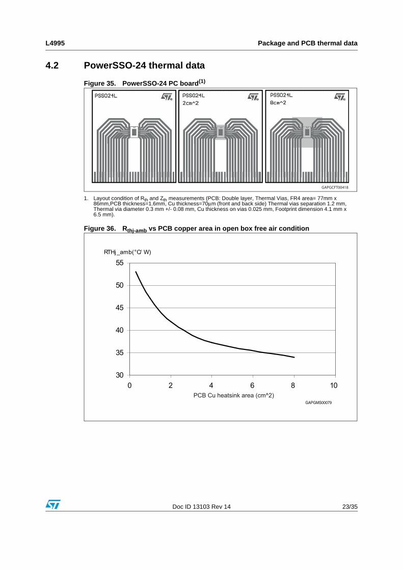
4.2 PowerSSO-24 thermal data
Figure 35. PowerSSO-24 PC board(1)
1. Layout condition of Rth and Zth measurements (PCB: Double layer, Thermal Vias, FR4 area= 77mm x 86mm,PCB thickness=1.6mm, Cu thickness=70μm (front and back side) Thermal vias separation 1.2 mm, Thermal via diameter 0.3 mm +/- 0.08 mm, Cu thickness on vias 0.025 mm, Footprint dimension 4.1 mm x 6.5 mm).
Figure 36. Rthj-amb vs PCB copper area in open box free air condition
GAPGCFT00418

Package and PCB thermal data L4995
24/35 Doc ID 13103 Rev 14
Figure 37. PowerSSO-24 thermal impedance junction ambient single pulse
Equation 5: pulse calculation formula
where δ = tP/T
Figure 38. Thermal fitting model of Vreg in PowerSSO-24
0,1
1
10
100
0,0001 0,001 0,01 0,1 1 10 100 1000Time (s)
ZTH (°C/ W)
Footprint
8 cm2
2 cm2
ZTHδ RTH δ ZTHtp 1 δ–( )+⋅=

L4995 Package and PCB thermal data
Doc ID 13103 Rev 14 25/35
Table 10. PowerSSO-24 thermal parameter
Area/island (cm2) Footprint 2 8
R1 (°C/W) 0.45
R2 (°C/W) 1.79
R3 (°C/W) 6
R4 (°C/W) 7.7
R5 (°C/W) 9 9 8
R6 (°C/W) 28 17 10
C1 (W.s/°C) 0.001
C2 (W.s/°C) 0.0022
C3 (W.s/°C) 0.025
C4 (W.s/°C) 0.75
C5 (W.s/°C) 1 4 9
C6 (W.s/°C) 2.2 5 17

Package and packing information L4995
26/35 Doc ID 13103 Rev 14
5 Package and packing information
5.1 ECOPACK®
In order to meet environmental requirements, ST offers these devices in different grades of ECOPACK® packages, depending on their level of environmental compliance. ECOPACK® specifications, grade definitions and product status are available at: www.st.com. ECOPACK® is an ST trademark.
Figure 39. PowerSSO-12 package dimensions

L4995 Package and packing information
Doc ID 13103 Rev 14 27/35
Table 11. PowerSSO-12 mechanical data
SymbolMillimeters
Min. Typ. Max.
A 1.250 1.620
A1 0.000 0.100
A2 1.100 1.650
B 0.230 0.410
C 0.190 0.250
D 4.800 5.000
E 3.800 4.000
e 0.800
H 5.800 6.200
h 0.250 0.500
L 0.400 1.270
k 0º 8º
X 2.200 2.800
Y 2.900 3.500
ddd 0.100

Package and packing information L4995
28/35 Doc ID 13103 Rev 14
5.2 PowerSSO-24 mechanical data
Figure 40. PowerSSO-24 package dimensions

L4995 Package and packing information
Doc ID 13103 Rev 14 29/35
Table 12. PowerSSO-24 mechanical data(1)(2)
1. No intrusion allowed inwards the leads.
2. Flash or bleeds on exposed die pad shall not exceed 0.4 mm per side
SymbolMillimeters
Min. Typ. Max.
A 2.45
A2 2.15 2.35
a1 0 0.10
b 0.33 0.51
c 0.23 0.32
D(3)
3. “D and E” do not include mold Flash or protusions.Mold Flash or protusions shall not exceed 0.15 mm.
10.10 10.50
E(3) 7.40 7.60
e 0.8
e3 8.8
F 2.3
G 0.1
G1 0.06
H 10.1 10.5
h 0.4
k 0° 8°
L 0.55 0.85
O 1.2
Q 0.8
S 2.9
T 3.65
U 1
N 10º
X 4.1 4.7
Y6.5
4.9(4)
4. Variations for small window leadframe option.
7.15.5(4)

Package and packing information L4995
30/35 Doc ID 13103 Rev 14
5.3 PowerSSO-12 packing information
Figure 41. PowerSSO-12 tube shipment (no suffix)
Figure 42. PowerSSO-12 tape and reel shipment (suffix “TR”)
All dimensions are in mm.
Base q.ty 100Bulk q.ty 2000Tube length (± 0.5) 532
A 1.85B 6.75C (± 0.1) 0.6
A
CB
Base q.ty 2500Bulk q.ty 2500
A (max) 330B (min) 1.5C (± 0.2) 13
F 20.2G (+ 2 / -0) 12.4N (min) 60
T (max) 18.4
REEL DIMENSIONS
TAPE DIMENSIONSAccording to Electronic Industries Association(EIA) Standard 481 rev. A, Feb. 1986
All dimensions are in mm.
Tape width W 12Tape hole spacing P0 (± 0.1) 4
Component spacing P 8Hole diameter D (± 0.05) 1.5Hole diameter D1 (min) 1.5
Hole position F (± 0.1) 5.5Compartment depth K (max) 4.5Hole spacing P1 (± 0.1) 2
Top
cover
tape
End
Start
No componentsNo components Components
500mm min
500mm minEmpty components pocketssaled with cover tape.
User direction of feed

L4995 Package and packing information
Doc ID 13103 Rev 14 31/35
5.4 PowerSSO-24 packing information
Figure 43. PowerSS0-24 tube shipment (no suffix)
Figure 44. PowerSSO-24 tape and reel shipment (suffix “TR”)
A
CB
GAPGCFT00002

Revision history L4995
32/35 Doc ID 13103 Rev 14
6 Revision history
Table 13. Document revision history
Date Revision Changes
26-May-2006 1 Initial release.
05-Jan-2007 2
L4995A and L4995R versions added:Features section updated and table added.Table 1 updated.
Table 5: General, Watchdog Iwi entry updated.Figure 2: Block diagram of L4995A and Figure 3: Block diagram of L4995R added.Table 2: Pins descriptions updated.Table 4: Thermal data updated.
List of tables and List of figures added.Packaging information provided in new format.Table 11: PowerSSO-12 mechanical data X and Y values updated.
Some sections reformatted for clarity.New disclaimer added.
18-May-2007 3Updated Table 2: Pins descriptions.Updated Figure 4: Pins configurations (L4995).Table 1: Device summary changed title.
09-Jul-2007 4 Updated Table 2: Pins descriptions.
09-Aug-2007 5Updated Table 2: Pins descriptions.Updated Table 12: PowerSSO-24 mechanical data.

L4995 Revision history
Doc ID 13103 Rev 14 33/35
07-Dec-2007 6
Updated Section 2.2: Thermal data: – corrected note changing single layer with double layer.
Updated Table 5: General: – changed Ishort typ. value from 750 to 800 mA– added Ishort max. value
– changed Ilim typ. value from 820 to 900 mA– added Ilim max. value– added Ilim note
– added Vdp note– changed Iqn_1 typ. value from 110 to 90 µA– added Iqn_1 max. value
– added Iqn_50 max. value– added Iqn_150 max. value– changed Iqn_250 typ. value from 1.2 to 1 mA
– added Iqn_250 max. value– changed Iqn_500 typ. value from 2.4 to 2.1 mA– added Iqn_500 max. value
Updated Table 6: Reset: – changed VRlth parameter definition from “Reset timing low” to
“Reset delay circuit low threshold”– changed VRhth parameter definition from “Reset timing high” to
“Reset delay circuit high threshold”– added Trd min. and max. valuesUpdated Table 7: Watchdog:
– added Iwi max valueUpdated Table 8: Enable: – changed Pull down current symbol from REn to IEn
– changed IEn typ. value from 2.5 to 10 µA– added IEn max. valueAdded Section 2.4: Electrical characteristics curves.
Added Section 2.5: Test circuit and waveforms plot.Added Section 4: Package and PCB thermal data
03-Oct-2008 7Updated PowerSSO-24 information:– changed Figure 40: PowerSSO-24 package dimensions– changed Table 12: PowerSSO-24 mechanical data.
19-Mar-2009 8 Updated Table 4: Thermal data
19-May-2009 9Updated Table 2: Pins descriptions.Updated Figure 4: Pins configurations (L4995)– Changed GND to substrate
Table 13. Document revision history (continued)
Date Revision Changes

Revision history L4995
34/35 Doc ID 13103 Rev 14
24-Jun-2009 10
Table 12: PowerSSO-24 mechanical data:– Deleted A (min) value
– Changed A (max) value from 2.50 to 2.45– Changed A2 (max) value from 2.40 to 2.35– Updated K row
– Changed L (min) value from 0.6 to 0.55– Changed L (max) value from 1 to 0.85
12-Jul-2010 11 Added Figure 27: Stability region(1).
09-Mar-2012 12 Added footnote in Table 3: Absolute maximum ratings.
17-Oct-2012 13Table 6: Reset:– Trd: updated min, typ and max values
20-Sep-2013 14 Updated disclaimer.
Table 13. Document revision history (continued)
Date Revision Changes

L4995
Doc ID 13103 Rev 14 35/35
Please Read Carefully:
Information in this document is provided solely in connection with ST products. STMicroelectronics NV and its subsidiaries (“ST”) reserve theright to make changes, corrections, modifications or improvements, to this document, and the products and services described herein at anytime, without notice.
All ST products are sold pursuant to ST’s terms and conditions of sale.
Purchasers are solely responsible for the choice, selection and use of the ST products and services described herein, and ST assumes noliability whatsoever relating to the choice, selection or use of the ST products and services described herein.
No license, express or implied, by estoppel or otherwise, to any intellectual property rights is granted under this document. If any part of thisdocument refers to any third party products or services it shall not be deemed a license grant by ST for the use of such third party productsor services, or any intellectual property contained therein or considered as a warranty covering the use in any manner whatsoever of suchthird party products or services or any intellectual property contained therein.
UNLESS OTHERWISE SET FORTH IN ST’S TERMS AND CONDITIONS OF SALE ST DISCLAIMS ANY EXPRESS OR IMPLIEDWARRANTY WITH RESPECT TO THE USE AND/OR SALE OF ST PRODUCTS INCLUDING WITHOUT LIMITATION IMPLIEDWARRANTIES OF MERCHANTABILITY, FITNESS FOR A PARTICULAR PURPOSE (AND THEIR EQUIVALENTS UNDER THE LAWSOF ANY JURISDICTION), OR INFRINGEMENT OF ANY PATENT, COPYRIGHT OR OTHER INTELLECTUAL PROPERTY RIGHT.
ST PRODUCTS ARE NOT DESIGNED OR AUTHORIZED FOR USE IN: (A) SAFETY CRITICAL APPLICATIONS SUCH AS LIFESUPPORTING, ACTIVE IMPLANTED DEVICES OR SYSTEMS WITH PRODUCT FUNCTIONAL SAFETY REQUIREMENTS; (B)AERONAUTIC APPLICATIONS; (C) AUTOMOTIVE APPLICATIONS OR ENVIRONMENTS, AND/OR (D) AEROSPACE APPLICATIONSOR ENVIRONMENTS. WHERE ST PRODUCTS ARE NOT DESIGNED FOR SUCH USE, THE PURCHASER SHALL USE PRODUCTS ATPURCHASER’S SOLE RISK, EVEN IF ST HAS BEEN INFORMED IN WRITING OF SUCH USAGE, UNLESS A PRODUCT ISEXPRESSLY DESIGNATED BY ST AS BEING INTENDED FOR “AUTOMOTIVE, AUTOMOTIVE SAFETY OR MEDICAL” INDUSTRYDOMAINS ACCORDING TO ST PRODUCT DESIGN SPECIFICATIONS. PRODUCTS FORMALLY ESCC, QML OR JAN QUALIFIED AREDEEMED SUITABLE FOR USE IN AEROSPACE BY THE CORRESPONDING GOVERNMENTAL AGENCY.
Resale of ST products with provisions different from the statements and/or technical features set forth in this document shall immediately voidany warranty granted by ST for the ST product or service described herein and shall not create or extend in any manner whatsoever, anyliability of ST.
ST and the ST logo are trademarks or registered trademarks of ST in various countries.Information in this document supersedes and replaces all information previously supplied.
The ST logo is a registered trademark of STMicroelectronics. All other names are the property of their respective owners.
© 2013 STMicroelectronics - All rights reserved
STMicroelectronics group of companies
Australia - Belgium - Brazil - Canada - China - Czech Republic - Finland - France - Germany - Hong Kong - India - Israel - Italy - Japan - Malaysia - Malta - Morocco - Philippines - Singapore - Spain - Sweden - Switzerland - United Kingdom - United States of America
www.st.com