7 w (10 w peak) 3 output supply using lnk626pg
TRANSCRIPT

Power Integrations
5245 Hellyer Avenue, San Jose, CA 95138 USA. Tel: +1 408 414 9200 Fax: +1 408 414 9201
www.powerint.com
DESIGN EXAMPLE REPORT
Title 7 W (10 W peak) 3 Output Supply Using LNK626PG
Specification 85 – 265 VAC Input; 5 V / 1.7 A, 12 V / 0.1 A, and -22 V / 15 mA Outputs
Application DVD Player
Author Applications Engineering Department
Document Number
DER-198
Date November 11, 2008
Revision 1.0
Summary and Features • Revolutionary control concept provides very low cost, low part-count solution
• Primary-side control eliminates secondary-side control and optocoupler
• Provides ±5% constant voltage (CV) accuracy Over-temperature protection – tight tolerance (±5%) with hysteretic recovery for
safe PCB temperatures under all conditions Auto-restart output short circuit and open-loop protection Extended pin creepage distance for reliable operation in humid environments –
>3.2 mm at package
• EcoSmart® – Easily meets all current international energy efficiency standards – China (CECP) / EISA / ENERGY STAR 2 / EU CoC Ultra-low leakage current: <5 µA at 265 VAC input (no Y capacitor required) Design easily passes EN550022 and CISPR-22 Class B EMI testing with >10 dB
margin
• Meets IEC 61000-4-5 Class 3 AC line surge
• Meets IEC 61000-4-2 ESD withstand (contact and air discharge to ±15 kV)
PATENT INFORMATION
The products and applications illustrated herein (including transformer construction and circuits external to the products) may be covered
by one or more U.S. and foreign patents, or potentially by pending U.S. and foreign patent applications assigned to Power Integrations. A
complete list of Power Integrations' patents may be found at www.powerint.com. Power Integrations grants its customers a license under
certain patent rights as set forth at <http://www.powerint.com/ip.htm>.

DER-198 – 7 W DVD Player 11-Nov-08
Page 2 of 40
Power IntegrationsTel: +1 408 414 9200 Fax: +1 408 414 9201 www.powerint.com
Table of Contents 1 Introduction.................................................................................................................4
2 Power Supply Specification ........................................................................................5
3 Schematic...................................................................................................................6
4 Circuit Description ......................................................................................................7
4.1 Input Section .......................................................................................................7
4.2 Input Filter ...........................................................................................................7
4.3 Primary Clamp.....................................................................................................8
4.4 Feedback.............................................................................................................8
4.5 Optional Bias Circuit ............................................................................................9
4.6 LinkSwitch-CV Bypass Capacitor ........................................................................9
4.7 Output Rectifiers and Filters ................................................................................9
4.8 Output Y Capacitor..............................................................................................9
5 PCB Layout ..............................................................................................................10
6 Bill of Materials .........................................................................................................11
7 Transformer Specification.........................................................................................12
7.1 Electrical Diagram .............................................................................................12
7.2 Electrical Specifications.....................................................................................12
7.3 Materials............................................................................................................12
7.4 Transformer Build Diagram ...............................................................................13
8 Transformer Spreadsheets.......................................................................................14
9 Performance Data ....................................................................................................17
9.1 Efficiency...........................................................................................................17
No-load Input Power ....................................................................................................18
9.2 Available Standby Output Power.......................................................................19
9.3 Regulation .........................................................................................................20
9.3.1 Load Regulation .........................................................................................20
9.3.2 Cross Regulation........................................................................................21
10 Thermal Performance ...........................................................................................24
11 Waveforms............................................................................................................25
11.1 Drain Voltage and Current, Normal Operation...................................................25
11.2 Output Voltage Start-up Profile..........................................................................25
11.3 Drain Voltage and Current Start-up Profile ........................................................26
11.4 Load Transient Response (50% to 100% Load Step) .......................................27
11.5 Output Ripple Measurements............................................................................28
11.5.1 Ripple Measurement Technique ................................................................28
11.5.2 Measurement Results ................................................................................29
12 Line Surge.............................................................................................................31
13 Conducted EMI .....................................................................................................32
14 Audible Noise........................................................................................................34
Revision History...............................................................................................................36

11-Nov-08 DER-198 – 7 W DVD Player
Page 3 of 40
Power Integrations Tel: +1 408 414 9200 Fax: +1 408 414 9201
www.powerint.com
Important Note: Although this board is designed to satisfy safety isolation requirements, the engineering prototype has not been agency approved. Therefore, all testing should be performed using an isolation transformer to provide the AC input to the prototype board.

DER-198 – 7 W DVD Player 11-Nov-08
Page 4 of 40
Power IntegrationsTel: +1 408 414 9200 Fax: +1 408 414 9201 www.powerint.com
1 Introduction
This document is an engineering report describing a DVD Player power supply utilizing a LNK626. This power supply is intended as a general purpose evaluation platform for LinkSwitch-CV. The document contains the power supply specification, schematic, bill of materials, transformer documentation, printed circuit layout, and performance data.
Figure 1 – Populated Circuit Board Photograph.

11-Nov-08 DER-198 – 7 W DVD Player
Page 5 of 40
Power Integrations Tel: +1 408 414 9200 Fax: +1 408 414 9201
www.powerint.com
2 Power Supply Specification
Description Symbol Min Typ Max Units Comment
Input
Voltage VIN 85 265 VAC 2 Wire – no P.E.
Frequency fLINE 47 50/60 64 Hz
No-load Input Power (230 VAC) 0.14 W
Output
Output Voltage 1 VOUT1 4.75 5.0 5.25 V ± 5%
Output Ripple Voltage 1 VRIPPLE1 100 mV 20 MHz bandwidth
Output Current 1 IOUT1 0.05 1.7 A Peak
Output Voltage 2 VOUT2 10.8 12 13.2 V ± 10%
Output Ripple Voltage 2 VRIPPLE2 750 mV 20 MHz bandwidth
Output Current 2 IOUT2 0.05 0.1 A
Output Voltage 3 VOUT3 -19.8 -22 -24.2 V ± 10%
Output Ripple Voltage 3 VRIPPLE3 200 mV 20 MHz bandwidth
Output Current 3 IOUT3 5 15 mA
Total Output Power
Continuous Output Power POUT 7 W
Peak Output Power POUT_PEAK 10 W
Efficiency
Full Load η 68.0 % Measured at POUT 25 o
C
Environmental
Conducted EMI Meets CISPR22B / EN55022B Output Floating
Safety Designed to meet IEC950 / UL1950
Class II
Surge Differential (L1-L2) Common Mode (L1/L2-PE) 100 kHz ring wave (L1/L2-PE)
2 6 6
kV kV kV
1.2/50 µs surge (per IEC 1000-4-5) Series Impedance:
12 Ω Common Mode
2 Ω Differential Mode
Ambient Temperature TAMB 0 40 oC Free convection, sea level

DER-198 – 7 W DVD Player 11-Nov-08
Page 6 of 40
Power IntegrationsTel: +1 408 414 9200 Fax: +1 408 414 9201 www.powerint.com
3 Schematic
Figure 2 – Schematic.

11-Nov-08 DER-198 – 7 W DVD Player
Page 7 of 40
Power Integrations Tel: +1 408 414 9200 Fax: +1 408 414 9201
www.powerint.com
4 Circuit Description
The LNK626PG was developed to be a cost effective solution in DVD Players, white goods, chargers or any application requiring a regulated constant voltage (CV) output. The LNK626PG has a monolithically integrated 700 V switching MOSFET and ON/OFF control function which together deliver high efficiency under all load conditions and low no-load energy consumption. Both the operating efficiency and no-load performance exceed all current international energy efficiency standards. The LNK626PG controller consists of an oscillator, a feedback (sense and logic) circuit, a 5.8 V regulator, over-temperature protection, frequency jittering, a current-limit circuit, leading-edge blanking and an ON/OFF state machine for CV control. The LNK626PG also provides a sophisticated range of protection features including auto-restart for control loop component open/short circuit faults and output short circuit conditions. Accurate hysteretic thermal shutdown ensures safe average PCB temperatures under all conditions. The IC package provides extended creepage distance between high and low voltage pins (both at the package and PCB), which is required in highly humid environments to prevent arcing and to further improve reliability. The LNK626PG can be configured to either be self-biased from the high-voltage DRAIN pin, or to receive an optional external bias supply. When configured to be self-biased, the very low IC current consumption ensures a worst-case no-load power consumption of less than 200 mW at 230 VAC. With external bias, <70 mW is achievable. This document contains the power supply specifications, schematic, bill of materials, transformer specifications, and typical performance characteristics for this reference design.
4.1 Input Section
Fuse F1 provides input current protection in case of a primary side component failure. Thermistor RT1 limits the inrush current when power is applied to the circuit. Metal oxide varistor RV1 provides differential line input surge protection, for surges greater than 2 kV. Below this level, RV1 may be omitted. Diodes D1 through D4 rectify the AC input, with D1 and D2 selected as a fast (500 ns) recovery to improve conducted EMI.
4.2 Input Filter
The AC input voltage is rectified by diodes D1 through D4 and filtered by C1 and C2.
Capacitors C1 and C2 together with L1 and L2 form a pi (π) filter to attenuate conducted EMI.

DER-198 – 7 W DVD Player 11-Nov-08
Page 8 of 40
Power IntegrationsTel: +1 408 414 9200 Fax: +1 408 414 9201 www.powerint.com
4.3 Primary Clamp
The drain clamp network is formed by R1, R2, C3, D5 and VR1. This network limits the leakage inductance inducted drain voltage spike. However unlike secondary side feedback the drain clamp design also affects the output regulation and ripple performance. Any ringing on the drain node also appears on the feedback winding and is therefore sampled by the FEEDBACK pin of U1. This can create an error between the output voltage and the sampled voltage seen by U1. This degrades regulation and output ripple.
Sampling occurs between 2.1 µs and 3.4 µs after the primary switch turn off. Therefore
ideally the drain voltage should settle to within ~1% of it’s final value (equal to VOR) 2.1 µs after turn off of the internal MOSFET. The goal of the clamp design is to reduce drain node ringing while limiting the peak drain voltage and minimizing dissipation for high efficiency and low no-load input power consumption. To meet this set of goals a Zener bleed clamp configuration was used. This is a RCD clamp where the resistor is replaced by the series combination of a resistor (R1) and low power Zener (VR1). The addition of the Zener prevents the clamp capacitor (C3) from being discharged below the Zener voltage rating at light or no-load that would normally occur with a standard RCD clamp. This improves light load efficiency and reduces no-load input power. The instantaneous current through VR1 is limited by R1 allowing a standard low cost, low power Zener (versus a transient voltage suppressor type). The value of VR1 is typically set 0%-20% above the value of VOR (the output voltage reflected through the transformer turns ratio). Here it was chosen as 110 V the same as the VOR to give the best possible output regulation. The value of R1 was selected to
discharge C3 to the value of VR1 in 2.1 µs. In designs with higher transformer leakage inductance the value of R1 may need to be increased to keep the dissipation of VR1 acceptable. For designs with primary leakage
inductance lower than ~100 µH, VR1 may be replaced with a single resistor in the range
of 100 kΩ to 470 kΩ. To prevent high frequency ringing D5 was selected as a standard recovery diode versus a fast or ultra-fast type. Resistor R2 acts to dampen the drain ringing, the value being chosen to dampen the drain ring to an acceptable level while keeping the peak drain voltage to below the BVDSS of the internal MOSFET.
4.4 Feedback
The ratio of R3 to R6 sets the output voltage level. The starting values are provided by the PI Xls design software. In some designs, C5 and R5 are required to eliminate excessive output ripple voltage caused by group pulsing. In LinkSwitch-CV applications, group pulsing is defined to be a group of five or more consecutive drain pulses followed

11-Nov-08 DER-198 – 7 W DVD Player
Page 9 of 40
Power Integrations Tel: +1 408 414 9200 Fax: +1 408 414 9201
www.powerint.com
by four or more skipped pulses. The value of R5 should be greater than or equal to the
value of 10xR6. The value of R5xC5 = 32 µs will provide optimum performance.
4.5 Optional Bias Circuit
Diodes D6, C6 and R4 along with a bias winding in the transformer provide an external bias supply. This circuit reduces the no load input power consumption to less than 150 mW (depending on the output preload resistor values) and increase efficiency. The components mentioned above may be removed if reduced no load input power and improved efficiency is not required.
4.6 LinkSwitch-CV Bypass Capacitor
LinkSwitch-CV requires a bypass capacitor of 1 µF minimum to bias the internal circuitry. The voltage rating must be greater than 6.8 V. Electrolytic, tantalum or ceramic dielectric may be used.
4.7 Output Rectifiers and Filters
Diodes D7 rectifies and C8, C10 and L3 filter the 5 V output. A diode rated at 5 A was chosen for D7 to improve cross regulation. If the cross regulation specification was relaxed or for single output applications, a smaller diode could be used. Resistor R10 and C13 form a snubber to reduce conducted and radiated EMI. Diode D8 and C9 rectify and filter the 12 V output. Diode D9 and C11 rectify and filter the -22 V output. Preload resistors R7, R8 and R9 limit the output voltages to safe levels in the event that the outputs become unloaded.
4.8 Output Y Capacitor
Capacitor C12 was not required to meet conducted EMI for a floating output test configuration. Other test configurations may require the use of a Y capacitor.

DER-198 – 7 W DVD Player 11-Nov-08
Page 10 of 40
Power IntegrationsTel: +1 408 414 9200 Fax: +1 408 414 9201 www.powerint.com
5 PCB Layout
Figure 3 – Printed Circuit Layout.

11-Nov-08 DER-198 – 7 W DVD Player
Page 11 of 40
Power Integrations Tel: +1 408 414 9200 Fax: +1 408 414 9201
www.powerint.com
6 Bill of Materials
Item Qty Ref Des Description Mfg Part Number Mfg
1 2 C1 C2
22 µF, 400 V, Electrolytic, Low ESR, 901 mOhm, (16 x 20) EKMX401ELL220ML20S Nippon Chemi-Con
2 1 C3 820 pF, 1 kV, Y5P, Disc Ceramic ECK-A3A821KBP Panasonic
3 1 C4 1.0 µF, 50 V, Ceramic, Z5U B37988G5105M000 Epcos
4 1 C5 680 pF, 50 V, Ceramic, COG B37979G5681J000 Epcos
5 1 C6 10 µF, 50 V, Electrolytic, Gen. Purpose, (5 x 11) EKMG500ELL100ME11D Nippon Chemi-Con
6 1 C8 1000 µF, 10 V, Electrolytic, Very Low ESR, 38 mΩ, (10 x 16) EKZE100ELL102MJ16S Nippon Chemi-Con
7 1 C9 47 µF, 25 V, Electrolytic, Low ESR, 500 mΩ, (5 x 11.5) ELXZ250ELL470MEB5D Nippon Chemi-Con
8 1 C10 470 µF, 10 V, Electrolytic, Very Low ESR, 72 mΩ, (8 x 11.5) EKZE100ELL471MHB5D Nippon Chemi-Con
9 1 C11 47 µF, 50 V, Electrolytic, Low ESR, 450 mΩ, (6.3 x 11.5) ELXZ500ELL470MFB5D Nippon Chemi-Con
10 1 C12 330 pF, Ceramic Y1 440LT33-R Vishay
11 1 C13 270 pF, 50 V, Ceramic, COG B37979N5271J000 Epcos
12 2 D1 D2
800 V, 1 A, Fast Recovery Diode, 500 ns, DO-41 FR106 Diodes Inc.
13 2 D3 D4
1000 V, 1 A, Rectifier, DO-41 1N4007-E3/54 Vishay
14 1 D5 1000 V, 1 A, Rectifier, DO-41 1N4007 Vishay
15 1 D6 75 V, 300 mA, Fast Switching, DO-35 1N4148 Vishay
16 1 D7 40 V, 5 A, Schottky, DO-201AD SB540 Vishay
17 2 D8 D9
200 V, 1 A, Ultrafast Recovery, 50 ns, DO-41 UF4003-E3 Vishay
18 1 F1 3.15A, 250V, TIME-LAG HI-BREAK TR5 38213150410 Wickman
19 1 J1 2 Position (1 x 2) header, 0.312 pitch, Vertical 26-50-3039 Molex
20 1 J2 6 Position (1 x 6) header, 2.5 mm pitch, Vertical DF1B-6P-2.5DSA Hirose Electric Co
21 1 JP1 Wire Jumper, Insulated, 22 AWG, 0.3 in C2004-12-02 Gen Cable
22 1 L1 3.5 mm x 7.6 mm, 75 Ω at 25 MHz, 22 AWG hole, Ferrite Bead
2743004112 Fair-Rite
23 1 L2 680 uH, 0.21 A, 7 x 10.5 mm SBC2-681-211 Tokin
24 1 L3 10 uH, 3.0 A R622LY-100K Toko
25 1 R1 5.1 k Ω, 5%, 1/4 W, Carbon Film CFR-25JB-5K1 Yageo
26 1 R2 390 Ω, 5%, 1/4 W, Carbon Film CFR-25JB-390R Yageo
27 1 R3 6.34 k Ω, 1%, 1/4 W, Metal Film MFR-25FBF-6K34 Yageo
28 1 R4 6.2 k Ω, 5%, 1/8 W, Carbon Film CFR-12JB-6K2 Yageo
29 1 R5 47 k Ω, 5%, 1/8 W, Carbon Film CFR-12JB-47K Yageo
30 1 R6 4.02 k Ω, 1%, 1/4 W, Metal Film MFR-25FBF-4K02 Yageo
31 1 R7 510 Ω, 5%, 1/8 W, Carbon Film CFR-12JB-510R Yageo
32 1 R8 24 k Ω, 5%, 1/8 W, Carbon Film CFR-12JB-24K Yageo
33 1 R9 39 k Ω, 5%, 1/8 W, Carbon Film CFR-12JB-39K Yageo
34 1 R10 47 Ω, 5%, 1/4 W, Carbon Film CFR-25JB-47R Yageo
35 1 RT1 NTC Thermistor, 10 Ohms, 1.7 A CL-120 Thermometrics
36 1 RV1 275 V, 80J, 10 mm, RADIAL ERZ-V10D431 Panasonic
37 1 T1 Transformer, EEL19 Horizontal 12 pin (5/7). Santronics SNX R1464
38 1 U1 LinkSwitch-II, LNK626PG, CV/CC, DIP-8C LNK626PG Power Integrations
39 1 VR1 110 V, 5%, 500 mW, DO-35 1N5272B Microsemi

DER-198 – 7 W DVD Player 11-Nov-08
Page 12 of 40
Power IntegrationsTel: +1 408 414 9200 Fax: +1 408 414 9201 www.powerint.com
7 Transformer Specification
7.1 Electrical Diagram
Figure 4 –Transformer Electrical Diagram.
7.2 Electrical Specifications
Electrical Strength 1 second, 60 Hz, from Pins 1-5 to Pins 6-12 4250 VAC
Primary Inductance Pins 1-3, all other windings open, measured at 100 kHz, 0.4 VRMS
1.62 µH, ±10%
Resonant Frequency Pins 1-3, all other windings open 375 kHz (Min.)
Primary Leakage Inductance Pins 1-3, with Pins 9-11 shorted, measured at
100 kHz, 0.4 VRMS 210 µH (Max.)
7.3 Materials
Item Description
[1] Core: EEL19 PC40 or equivalent. Gapped to 40.5 nH/T2
[2] Bobbin: EEL19 Horizontal 12 pin (5/7).

11-Nov-08 DER-198 – 7 W DVD Player
Page 13 of 40
Power Integrations Tel: +1 408 414 9200 Fax: +1 408 414 9201
www.powerint.com
7.4 Transformer Build Diagram
Figure 5 – Transformer Build Diagram.

DER-198 – 7 W DVD Player 11-Nov-08
Page 14 of 40
Power IntegrationsTel: +1 408 414 9200 Fax: +1 408 414 9201 www.powerint.com
8 Transformer Spreadsheets 7 Watt (10 W Peak) DVD Application
INPUT INFO OUTPUT UNIT ACDC_LNK-CV_080508_Rev0-5.xls; LinkSwitch-CV Continuous/Discontinuous Flyback Transformer Design Spreadsheet
ENTER APPLICATION VARIABLES Customer VACMIN 85 Volts Minimum AC Input Voltage VACMAX 265 Volts Maximum AC Input Voltage fL 50 Hertz AC Mains Frequency VO 5.00 Volts Output Voltage
PO 10.00 Watts Output Power n 0.68 Efficiency Estimate Z 0.5 Loss Allocation Factor tC 3.50 3.5 mSecon
ds Bridge Rectifier Conduction Time Estimate
CIN 44.00 uFarads Input Filter Capacitor
ENTER LinkSwitch-CV VARIABLES LinkSwitch-CV LNK626P Univers
al 115 Doubled/230V
Chosen Device LNK626P Power Out 10W 17W ILIMITMIN 0.419 Amps LinkSwitch-CV Minimum Current Limit ILIMITMAX 0.482 Amps LinkSwitch-CV Maximum Current Limit fS 100000 Hertz LinkSwitch-CV Switching Frequency I2FMIN 18225 Hertz LinkSwitch-CV Min I2F (power Co-efficienct) I2FMAX 23693 Hertz LinkSwitch-CV Max I2F (power Co-efficienct) VOR 110.00 110 Volts Reflected Output Voltage VDS 10 Volts LinkSwitch-CV on-state Drain to Source Voltage VD 0.5 Volts Output Winding Diode Forward Voltage Drop DCON 5.58 us Output Diode conduction time KP_TRANSIENT 0.70 Worst case ripple to peak current ratio. Maintain
KP_TRANSIENT below 0.25 KP 0.73 Ripple to Peak Current Ratio (0.4<KRP<1.0 :
1.0<KDP<6.0)
ENTER TRANSFORMER CORE/CONSTRUCTION VARIABLES Core Type EEL19 Core EEL19 P/N: PC40EE19/27/5-Z Bobbin EEL19_BOBBIN P/N: * AE 0.2454 cm^2 Core Effective Cross Sectional Area LE 6.185 cm Core Effective Path Length AL 720 nH/T^2 Ungapped Core Effective Inductance BW 19.7 mm Bobbin Physical Winding Width M 4.50 mm Safety Margin Width (Half the Primary to
Secondary Creepage Distance) L 3.00 3 Number of Primary Layers NS 10.00 10 Number of Secondary Turns
DC INPUT VOLTAGE PARAMETERS VMIN 101 Volts Minimum DC Input Voltage VMAX 375 Volts Maximum DC Input Voltage
Bias Winding Parameters Add Bias winding YES Enter Yes if you want to add a Bias winding NB Number of Bias winding turns - AC stacked on
Feedback winding
CURRENT WAVEFORM SHAPE PARAMETERS DMAX 0.55 Maximum Duty Cycle IAVG 0.15 Amps Average Primary Current IP 0.42 Amps Minimum Peak Primary Current IR 0.30 Amps Primary Ripple Current IRMS 0.21 Amps Primary RMS Current

11-Nov-08 DER-198 – 7 W DVD Player
Page 15 of 40
Power Integrations Tel: +1 408 414 9200 Fax: +1 408 414 9201
www.powerint.com
TRANSFORMER PRIMARY DESIGN PARAMETERS LPMIN 1465 uHenrie
s Minimum Primary Inductance
LP_TOL 10 NP 200 Primary Winding Number of Turns ALG 37 nH/T^2 Gapped Core Effective Inductance BM 1438 Gauss Maximum Flux Density, (BP<3100) BAC 455 Gauss AC Flux Density for Core Loss Curves (0.5 X
Peak to Peak) ur 1444 Relative Permeability of Ungapped Core LG 0.80 mm Gap Length (Lg > 0.1 mm) BWE 32.1 mm Effective Bobbin Width OD 0.16 mm Maximum Primary Wire Diameter including
insulation INS 0.04 mm Estimated Total Insulation Thickness (= 2 * film
thickness) DIA 0.12 mm Bare conductor diameter AWG 37 AWG Primary Wire Gauge (Rounded to next smaller
standard AWG value) CM 20 Cmils Bare conductor effective area in circular mils CMA Warning 97 Cmils/A
mp !!! INCREASE CMA>200 (increase L(primary layers),decrease NS,larger Core)
TRANSFORMER SECONDARY DESIGN PARAMETERS Lumped parameters ISP 8.38 Amps Peak Secondary Current ISRMS 3.77 Amps Secondary RMS Current IO 2.00 Amps Power Supply Output Current IRIPPLE 3.20 Amps Output Capacitor RMS Ripple Current CMS 755 Cmils Secondary Bare Conductor minimum circular
mils AWGS 21 AWG Secondary Wire Gauge (Rounded up to next
larger standard AWG value) DIAS 0.73 mm Secondary Minimum Bare Conductor Diameter ODS 1.07 mm Secondary Maximum Outside Diameter for
Triple Insulated Wire INSS 0.17 mm Maximum Secondary Insulation Wall Thickness
VOLTAGE STRESS PARAMETERS VDRAIN 626 Volts Maximum Drain Voltage Estimate (Includes
Effect of Leakage Inductance) PIVS 24 Volts Output Rectifier Maximum Peak Inverse Voltage
FEEDBACK VARIABLES NFB 9.00 Feedback winding number of turns RUPPER 9.05 k-ohms Upper resistor of feedback network RLOWER 6.13 k-ohms Lower resistor of feedback network
TRANSFORMER SECONDARY DESIGN PARAMETERS (MULTIPLE OUTPUTS) 1st output VO1 5.00 5 Volts Output Voltage (if unused, defaults to single
output design) IO1 1.70 1.700 Amps Output DC Current PO1 8.50 Watts Output Power VD1 0.5 Volts Output Diode Forward Voltage Drop
NS1 10.00 Output Winding Number of Turns ISRMS1 3.207 Amps Output Winding RMS Current IRIPPLE1 2.72 Amps Output Capacitor RMS Ripple Current PIVS1 24 Volts Output Rectifier Maximum Peak Inverse Voltage CMS1 641 Cmils Output Winding Bare Conductor minimum
circular mils AWGS1 22 AWG Wire Gauge (Rounded up to next larger
standard AWG value) DIAS1 0.65 mm Minimum Bare Conductor Diameter

DER-198 – 7 W DVD Player 11-Nov-08
Page 16 of 40
Power IntegrationsTel: +1 408 414 9200 Fax: +1 408 414 9201 www.powerint.com
ODS1 1.07 mm Maximum Outside Diameter for Triple Insulated Wire
2nd output VO2 12.00 Volts Output Voltage IO2 0.10 Amps Output DC Current PO2 1.20 Watts Output Power VD2 0.7 Volts Output Diode Forward Voltage Drop NS2 23.09 Output Winding Number of Turns
ISRMS2 0.189 Amps Output Winding RMS Current IRIPPLE2 0.16 Amps Output Capacitor RMS Ripple Current PIVS2 55 Volts Output Rectifier Maximum Peak Inverse Voltage
CMS2 38 Cmils Output Winding Bare Conductor minimum
circular mils AWGS2 34 AWG Wire Gauge (Rounded up to next larger
standard AWG value) DIAS2 0.16 mm Minimum Bare Conductor Diameter ODS2 0.46 mm Maximum Outside Diameter for Triple Insulated
Wire
3rd output VO3 22.00 Volts Output Voltage IO3 0.02 Amps Output DC Current PO3 0.33 Watts Output Power VD3 0.7 Volts Output Diode Forward Voltage Drop NS3 41.27 Output Winding Number of Turns ISRMS3 0.028 Amps Output Winding RMS Current IRIPPLE3 0.02 Amps Output Capacitor RMS Ripple Current PIVS3 99 Volts Output Rectifier Maximum Peak Inverse Voltage
CMS3 6 Cmils Output Winding Bare Conductor minimum
circular mils AWGS3 42 AWG Wire Gauge (Rounded up to next larger
standard AWG value) DIAS3 0.06 mm Minimum Bare Conductor Diameter ODS3 0.26 mm Maximum Outside Diameter for Triple Insulated
Wire
Total power 10.03 Watts Total Output Power
Negative Output 3 3 Output # 3 is negative output
Notes:
• Primary winding CMA warning is allowed because this occurs during peak loading. CMA is higher under normal operation.
• Rupper and Rlower values may be different in the actual assembly due to tuning of output voltages.
• The -22 V winding turns was adjusted from 41 to 40 turns to center the output voltage.
• The transformer was designed with a flux density below 1500 Gauss (150 mT) to reduce audible noise generation from the transformer. A flux density around this level is recommended when using long cores (EEL vs EE). Higher flux densities are possible for EE cores or with EEL cores where higher levels of audible noise are acceptable.

11-Nov-08 DER-198 – 7 W DVD Player
Page 17 of 40
Power Integrations Tel: +1 408 414 9200 Fax: +1 408 414 9201
www.powerint.com
9 Performance Data
All measurements performed at room temperature, 60 Hz input frequency.
9.1 Efficiency
50%
55%
60%
65%
70%
75%
80%
0 2 4 6 8 10 12
Output Power (W)
Eff
icie
nc
y
Vin = 85 VAC
Vin = 115 VAC
Vin = 230 VAC
Vin = 265 VAC
Figure 6 – Efficiency vs. Input Voltage, Room Temperature, 60 Hz.

DER-198 – 7 W DVD Player 11-Nov-08
Page 18 of 40
Power IntegrationsTel: +1 408 414 9200 Fax: +1 408 414 9201 www.powerint.com
No-load Input Power
0
0.05
0.1
0.15
0.2
0.25
0.3
0 50 100 150 200 250 300
Vin (VAC)
Inp
ut
Po
wer
(W)
Figure 7 – Zero Load Input Power vs. Input Line Voltage, Room Temperature, 60 Hz.

11-Nov-08 DER-198 – 7 W DVD Player
Page 19 of 40
Power Integrations Tel: +1 408 414 9200 Fax: +1 408 414 9201
www.powerint.com
9.2 Available Standby Output Power
The chart below shows the available output power vs line voltage for an input power of 1 W, 0.5 W and 0.3 W.
0
0.1
0.2
0.3
0.4
0.5
0.6
0.7
0 50 100 150 200 250 300
Vin (VAC)
Po
ut
(W)
Pin = 0.3 W
Pin = 0.5 W
Pin = 1 W
Figure 8 – Available Standby Power.

DER-198 – 7 W DVD Player 11-Nov-08
Page 20 of 40
Power IntegrationsTel: +1 408 414 9200 Fax: +1 408 414 9201 www.powerint.com
9.3 Regulation
9.3.1 Load Regulation
The 5 Volt output current was varied from 0.05 Amp to 1.75 Amps. The +12 V current was constant at 0.1 Amp and the -22 V current was constant at 15 mA.
4
4.2
4.4
4.6
4.8
5
5.2
5.4
5.6
5.8
6
0 0.2 0.4 0.6 0.8 1 1.2 1.4 1.6 1.8
Amps
Vo
lts
Vin=85 VAC
Vin=115 VAC
Vin=230 VAC
Vin=265 VAC
5 Volt Limits
5 Volt Limits
Figure 9 – Load Regulation, Room Temperature.

11-Nov-08 DER-198 – 7 W DVD Player
Page 21 of 40
Power Integrations Tel: +1 408 414 9200 Fax: +1 408 414 9201
www.powerint.com
9.3.2 Cross Regulation
The figures below show the output voltage vs. total output power. The charts show the voltage variations as the loads vary for all legal load combinations. The 5 V current varied from 50 mA to 1.75 Amps. The 12 V output current varied from 50 mA to 100 mA. The -22 V output current varied from 5 mA to 15 mA.
4
4.2
4.4
4.6
4.8
5
5.2
5.4
5.6
5.8
6
0 1 2 3 4 5 6 7 8 9 10
Output Power
Vo
lts
Vin=85 VAC
Vin=115 VAC
Vin=230 VAC
Vin=265 VAC
5 Volt Limits
5 Volt Limits
Figure 10 – 5 V Cross Regulation, Room Temperature.

DER-198 – 7 W DVD Player 11-Nov-08
Page 22 of 40
Power IntegrationsTel: +1 408 414 9200 Fax: +1 408 414 9201 www.powerint.com
8
9
10
11
12
13
14
15
16
0 1 2 3 4 5 6 7 8 9 10
Output Power
Vo
lts
Vin=85 VAC
Vin=115 VAC
Vin=230 VAC
Vin=265 VAC
12 Volt Limits
12 Volt Limits
Figure 11 – 12 V Cross Regulation, Room Temperature.
-25
-24
-23
-22
-21
-20
-19
-18
-17
-16
-15
0 1 2 3 4 5 6 7 8 9 10
Output Power
Vo
lts
Vin=85 VAC
Vin=115 VAC
Vin=230 VAC
Vin=265 VAC
22 Volt Limits
22 Volt Limits
Figure 12 – 22 V Cross Regulation, Room Temperature.

11-Nov-08 DER-198 – 7 W DVD Player
Page 23 of 40
Power Integrations Tel: +1 408 414 9200 Fax: +1 408 414 9201
www.powerint.com
The graphs below show the output Voltage and load currents required to power a DVD player. The graphs represent the current demand as the DVD player is exercised in all operating modes. The Model used was a Philips DVP 5990.
3
3.5
4
4.5
5
5.5
6
0 5 10 15 20 25 30 35 40 45
Time (seconds)
Vo
lts
0
0.5
1
1.5
2
2.5
3
Am
ps
5 Volt Limits
5 Volt Limits
5 Volt Output
5 Volt Current Amps
5
6
7
8
9
10
11
12
13
14
15
0 5 10 15 20 25 30 35 40 45
Time (seconds)
Vo
lts
0
0.02
0.04
0.06
0.08
0.1
0.12
0.14
0.16
0.18
0.2
Am
ps
12 Volts out Volt
12 Volt Limits
12 Volt Limits
12 Volt Current
-30
-28
-26
-24
-22
-20
-18
-16
-14
-12
-10
0 5 10 15 20 25 30 35 40 45
Time (seconds)
Vo
lts
-50
-45
-40
-35
-30
-25
-20
-15
-10
-5
0
Cu
rre
nt
(mA
)
22 Volts Out
22 Volt Limit
22 Volt Limit
22 Volt Current (mA)
Figure 13 – Voltage Regulation and Current Demands in DVD Application.

DER-198 – 7 W DVD Player 11-Nov-08
Page 24 of 40
Power IntegrationsTel: +1 408 414 9200 Fax: +1 408 414 9201 www.powerint.com
10 Thermal Performance
The power supply was placed inside a cardboard box (no air flow) in the temperature chamber. The loads are as follows: 5 V at 1 Amp 12 V at 0.1 Amp -22 V at 15 mA This load represents a typical DVD player Load during Play Mode. The ambient temperature was measured inside the cardboard box.
Temperature Deg C Item
85 VAC 115 VAC 230 VAC 265 VAC
Ambient 40 40 40 40
Clamp Zener (VR1) 88.9 84.8 82.7 83.0
LNK626 (U1) 68.0 65.1 66.4 65.0

11-Nov-08 DER-198 – 7 W DVD Player
Page 25 of 40
Power Integrations Tel: +1 408 414 9200 Fax: +1 408 414 9201
www.powerint.com
11 Waveforms
11.1 Drain Voltage and Current, Normal Operation
Figure 14 – 85 VAC, Full Load (10 W).
Upper: VDRAIN, 100 V, 10 µs / div. Lower: IDRAIN, 0.2 A / div.
Figure 15 – 265 VAC, Full Load (10 W).
Upper: VDRAIN, 200 V, 10 µs / div. Lower: IDRAIN, 0.2 A / div.
11.2 Output Voltage Start-up Profile
Figure 16 – 5 V Start-up Profile, 115 VAC 1 V, 20 ms / div.
Figure 17 – 5 V Start-up Profile, 230 VAC 1 V, 20 ms / div.

DER-198 – 7 W DVD Player 11-Nov-08
Page 26 of 40
Power IntegrationsTel: +1 408 414 9200 Fax: +1 408 414 9201 www.powerint.com
11.3 Drain Voltage and Current Start-up Profile
Figure 18 – 85 VAC Input and Maximum Load. Upper: VDRAIN, 200 V, 1 ms / div. Lower: IDRAIN, 0.2 A / div.
Figure 19 – 265 VAC Input and Maximum Load. Upper: VDRAIN, 200 V, 1 ms / div. Lower: IDRAIN, 0.2 A / div.

11-Nov-08 DER-198 – 7 W DVD Player
Page 27 of 40
Power Integrations Tel: +1 408 414 9200 Fax: +1 408 414 9201
www.powerint.com
11.4 Load Transient Response (50% to 100% Load Step)
In the figures shown below, signal averaging was used to better enable viewing the load transient response. The oscilloscope was triggered using the load current step as a trigger source. Since the output switching and line frequency occur essentially at random with respect to the load transient, contributions to the output ripple from these sources will average out, leaving the contribution only from the load step response.
Figure 20 – Transient Response,
115 VAC, 5 V Load Step: 0.55 A – 1.10 A -0.55 A 5 V Output 50 mV, 200 ms / div.
Figure 21 – Transient Response,
115 VAC, 12 V Output Response During 5 V Transient.
50 mV, 200 ms/div.
Figure 22 – Transient Response,
115 VAC, -22 V Output Response During 5 V Transient.
50 mV, 200 ms/div.
Figure 23 – Transient Response,
230 VAC, 5 V Load Step: 0.55 A – 1.10 A -0.55 A 5 V Output 50 mV, 200 ms / div.
Figure 24 – Transient Response,
230 VAC, 12 V Output Response During 5 V Transient.
50 mV, 200 ms / div.
Figure 25 – Transient Response,
230 VAC, -22 V Output Response During 5 V Transient.
50 mV, 200 ms / div.

DER-198 – 7 W DVD Player 11-Nov-08
Page 28 of 40
Power IntegrationsTel: +1 408 414 9200 Fax: +1 408 414 9201 www.powerint.com
11.5 Output Ripple Measurements
11.5.1 Ripple Measurement Technique
For DC output ripple measurements, use a modified oscilloscope test probe to reduce spurious signals. Details of the probe modification are provided in the figures below. Tie two capacitors in parallel across the probe tip of the 4987BA probe adapter. Use a
0.1 µF/50 V ceramic capacitor and a 1.0 µF/50 V aluminum-electrolytic capacitor. The aluminum-electrolytic capacitor is polarized, so always maintain proper polarity across DC outputs.
Figure 26 – Oscilloscope Probe Prepared for Ripple Measurement. (End Cap and Ground Lead Removed)
Figure 27 – Oscilloscope Probe with Probe Master (www.probemaster.com) 4987A BNC Adapter. (Modified with wires for ripple measurement, and two parallel decoupling capacitors added)
Probe Ground
Probe Tip

11-Nov-08 DER-198 – 7 W DVD Player
Page 29 of 40
Power Integrations Tel: +1 408 414 9200 Fax: +1 408 414 9201
www.powerint.com
11.5.2 Measurement Results
Unless otherwise specified, full load is: 5 Volts @ 1.10 A 12 Volts @ 0.10 A -22 Volts @ 0.015 A
Figure 28 – 5 V Ripple, 85 VAC, Full Load (7W) 10 ms, 20 mV / div. Ripple: 38 mVp-p.
Figure 29 – 12 V Ripple, 85 VAC, Full Load.
10 µs, 100 mV / div. Ripple: 268 mVp-p.
Figure 30 – -22 V Ripple, 85 VAC, Full Load.
100 µs, 20 mV / div. Ripple: 72 mVp-p.
Figure 31 – 5 V Ripple, 115 VAC, Full Load (7 W). 10 ms, 20 mV / div. Ripple: 40 mVp-p.
Figure 32 – 12 V Ripple, 115 VAC, Full Load.
20 µs, 100 mV / div. Ripple: 288 mVp-p.
Figure 33 – -22 V Ripple, 115 VAC, Full Load.
100 µs, 20 mV / div. Ripple: 70 mVp-p.
Figure 34 – 5 V Ripple, 230 VAC, Full Load (7W). 10 ms, 20 mV /div. Ripple: 40 mVp-p.
Figure 35 – 12 V Ripple, 230 VAC, Full Load.
20 µs, 100 mV / div. Ripple: 258 mVp-p.
Figure 36 – -22 V Ripple, 230 VAC,Full Load.
100 µs, 20 mV / div. Ripple: 72 mVp-p.

DER-198 – 7 W DVD Player 11-Nov-08
Page 30 of 40
Power IntegrationsTel: +1 408 414 9200 Fax: +1 408 414 9201 www.powerint.com
Figure 37 – 5 V Ripple, 265 VAC,
Full Load (7 W). 10 µs, 20 mV /div. Ripple: 33 mVp-p.
Figure 38 – 12 V Ripple, 265 VAC,
Full Load. 20 µs, 100 mV / div. Ripple: 308 mVp-p.
Figure 39 – -22 V Ripple, 265 VAC,
Full Load. 100 µs, 20 mV / div. Ripple: 80 mVp-p.
11-Nov-08 DER-198 – 7 W DVD Player
Page 31 of 40
Power Integrations Tel: +1 408 414 9200 Fax: +1 408 414 9201
www.powerint.com
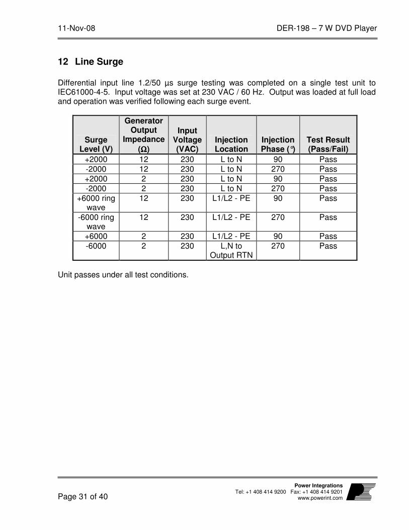
12 Line Surge
Differential input line 1.2/50 µs surge testing was completed on a single test unit to IEC61000-4-5. Input voltage was set at 230 VAC / 60 Hz. Output was loaded at full load and operation was verified following each surge event.
Surge Level (V)
Generator Output
Impedance
(ΩΩΩΩ)
Input Voltage (VAC)
Injection Location
Injection Phase (°)
Test Result (Pass/Fail)
+2000 12 230 L to N 90 Pass
-2000 12 230 L to N 270 Pass
+2000 2 230 L to N 90 Pass
-2000 2 230 L to N 270 Pass
+6000 ring wave
12 230 L1/L2 - PE 90 Pass
-6000 ring wave
12 230 L1/L2 - PE 270 Pass
+6000 2 230 L1/L2 - PE 90 Pass
-6000 2 230 L,N to Output RTN
270 Pass
Unit passes under all test conditions.

DER-198 – 7 W DVD Player 11-Nov-08
Page 32 of 40
Power IntegrationsTel: +1 408 414 9200 Fax: +1 408 414 9201 www.powerint.com
13 Conducted EMI
Conducted EMI was measured with the power supply operating a DVD Player. Six plots show the conducted EMI for 115 VAC and 230 VAC and with the player in Standby Mode, On Mode (no disk in payer) and Play Mode. The DVD player chassis was not grounded for these measurements. Other testing configurations may require a Y capacitor to meet EMI requirements.
Power Integrations
2 AV
CLRWR
SGL
6DB
1 QP
CLRWR
TDF
dBµV
dBµV
150 kHz 30 MHz
RBW 9 kHz
MT 20 ms
Att 10 dB AUTO
11.Aug 08 08:51
1 MHz 10 MHz
-20
-10
0
10
20
30
40
50
60
70
80
LIMIT CHECK PASS
1
Marker 1 [T1 ]
29.56 dBµV
182.849162999 kHz
EN55022A
EN55022Q
Power Integrations
150 kHz 30 MHz
1 QP
CLRWR
2 AV
CLRWR
SGL
TDF
6DB
dBµV
dBµV
11.Aug 08 09:05
RBW 9 kHz
MT 500 ms
Att 10 dB AUTO
1 MHz 10 MHz
-20
-10
0
10
20
30
40
50
60
70
80
LIMIT CHECK MARG
LINE EN55022A MARG
LINE EN55022Q MARG
1
Marker 1 [T1 ]
34.00 dBµV
182.849162999 kHz
EN55022A
EN55022Q
Power Integrations
150 kHz 30 MHz
1 QP
CLRWR
2 AV
CLRWR
SGL
TDF
6DB
dBµV
dBµV
RBW 9 kHz
MT 500 ms
Att 10 dB AUTO
11.Aug 08 09:23
1 MHz 10 MHz
-20
-10
0
10
20
30
40
50
60
70
80
LIMIT CHECK MARG
LINE EN55022A MARG
LINE EN55022Q MARG
1
Marker 1 [T1 ]
36.14 dBµV
182.849162999 kHz
EN55022A
EN55022Q
No peak summary (>20 dB margin)
DVD Player In Standby Mode.
Vin = 115 VAC. DVD Player In ON Mode.
Vin = 115 VAC. DVD Player In Play Mode.
Vin = 115 VAC.
Figure 43 – Conducted EMI, Maximum Steady State Load, 115 VAC, 60 Hz, and EN55022 B Limits.

11-Nov-08 DER-198 – 7 W DVD Player
Page 33 of 40
Power Integrations Tel: +1 408 414 9200 Fax: +1 408 414 9201
www.powerint.com
Power Integrations
150 kHz 30 MHz
1 QP
CLRWR
2 AV
CLRWR
SGL
TDF
6DB
dBµV
dBµV
RBW 9 kHz
MT 500 ms
Att 10 dB AUTO
11.Aug 08 10:25
1 MHz 10 MHz
-20
-10
0
10
20
30
40
50
60
70
80
LIMIT CHECK MARG
LINE EN55022Q MARG
1
Marker 1 [T1 ]
32.31 dBµV
182.849162999 kHz
EN55022A
EN55022Q
Power Integrations
150 kHz 30 MHz
1 QP
CLRWR
2 AV
CLRWR
SGL
TDF
6DB
dBµV
dBµV
RBW 9 kHz
MT 500 ms
Att 20 dB AUTO
11.Aug 08 10:10
1 MHz 10 MHz
-20
-10
0
10
20
30
40
50
60
70
80
LIMIT CHECK MARG
LINE EN55022A MARG
LINE EN55022Q MARG
1
Marker 1 [T1 ]
39.03 dBµV
182.849162999 kHz
EN55022A
EN55022Q
Power Integrations
150 kHz 30 MHz
1 QP
CLRWR
2 AV
CLRWR
SGL
TDF
6DB
dBµV
dBµV
RBW 9 kHz
MT 500 ms
Att 10 dB AUTO
11.Aug 08 09:54
1 MHz 10 MHz
-20
-10
0
10
20
30
40
50
60
70
80
LIMIT CHECK MARG
LINE EN55022A MARG
LINE EN55022Q MARG
1
Marker 1 [T1 ]
41.18 dBµV
182.849162999 kHz
EN55022A
EN55022Q
DVD Player In Standby Mode. Vin = 230 VAC.
DVD Player In ON Mode. Vin = 230 VAC.
DVD Player In Play Mode. Vin = 230 VAC.
Figure 44 – Conducted EMI, Maximum Steady State Load, 230 VAC, 60 Hz, and EN55022 B Limits.

DER-198 – 7 W DVD Player 11-Nov-08
Page 34 of 40
Power IntegrationsTel: +1 408 414 9200 Fax: +1 408 414 9201 www.powerint.com
14 Audible Noise
The power supply’s audible noise was measured while operating a DVD Player. With the case removed the microphone was placed 2 cm directly above the transformer. Measurements were made with a calibrated microphone and Audio Precision System II audio analyzer. Audio levels below 35 dBA measured in this way are considered inaudible when the case in fitted.
Figure 45 – DVD Player in Standby Mode.
Vin = 115 VAC.
Figure 46 – DVD Player in On Mode.
Vin = 115 VAC.

11-Nov-08 DER-198 – 7 W DVD Player
Page 35 of 40
Power Integrations Tel: +1 408 414 9200 Fax: +1 408 414 9201
www.powerint.com
Figure 47 – DVD Player in Play Mode
Vin = 115 VAC.

DER-198 – 7 W DVD Player 11-Nov-08
Page 36 of 40
Power IntegrationsTel: +1 408 414 9200 Fax: +1 408 414 9201 www.powerint.com
Revision History
Date Author Revision Description & changes Reviewed 11-Nov-08 JAC 1.0 Initial Release PV

11-Nov-08 DER-198 – 7 W DVD Player
Page 37 of 40
Power Integrations Tel: +1 408 414 9200 Fax: +1 408 414 9201
www.powerint.com
Notes

DER-198 – 7 W DVD Player 11-Nov-08
Page 38 of 40
Power IntegrationsTel: +1 408 414 9200 Fax: +1 408 414 9201 www.powerint.com
Notes

11-Nov-08 DER-198 – 7 W DVD Player
Page 39 of 40
Power Integrations Tel: +1 408 414 9200 Fax: +1 408 414 9201
www.powerint.com
Notes

DER-198 – 7 W DVD Player 11-Nov-08
Page 40 of 40
Power IntegrationsTel: +1 408 414 9200 Fax: +1 408 414 9201 www.powerint.com
For the latest updates, visit our website: www.powerint.com
Power Integrations reserves the right to make changes to its products at any time to improve reliability or
manufacturability. Power Integrations does not assume any liability arising from the use of any device or circuit
described herein. POWER INTEGRATIONS MAKES NO WARRANTY HEREIN AND SPECIFICALLY DISCLAIMS ALL
WARRANTIES INCLUDING, WITHOUT LIMITATION, THE IMPLIED WARRANTIES OF MERCHANTABILITY,
FITNESS FOR A PARTICULAR PURPOSE, AND NON-INFRINGEMENT OF THIRD PARTY RIGHTS.
PATENT INFORMATION
The products and applications illustrated herein (including transformer construction and circuits external to the products)
may be covered by one or more U.S. and foreign patents, or potentially by pending U.S. and foreign patent applications
assigned to Power Integrations. A complete list of Power Integrations’ patents may be found at www.powerint.com.
Power Integrations grants its customers a license under certain patent rights as set forth at
http://www.powerint.com/ip.htm.
The PI Logo, TOPSwitch, TinySwitch, LinkSwitch, DPA-Switch, PeakSwitch, EcoSmart, Clampless, E-Shield, Filterfuse, StackFET,
PI Expert and PI FACTS are trademarks of Power Integrations, Inc. Other trademarks are property of their respective
companies. ©Copyright 2008 Power Integrations, Inc.
Power Integrations Worldwide Sales Support Locations
WORLD HEADQUARTERS 5245 Hellyer Avenue San Jose, CA 95138, USA. Main: +1-408-414-9200 Customer Service: Phone: +1-408-414-9665 Fax: +1-408-414-9765 e-mail: [email protected]
GERMANY Rueckertstrasse 3 D-80336, Munich Germany Phone: +49-89-5527-3911 Fax: +49-89-5527-3920 e-mail: [email protected]
JAPAN Kosei Dai-3 Bldg., 2-12-11, Shin-Yokohama, Kohoku-ku, Yokohama-shi, Kanagawa 222-0033 Phone: +81-45-471-1021 Fax: +81-45-471-3717 e-mail: [email protected]
TAIWAN 5F, No. 318, Nei Hu Rd., Sec. 1 Nei Hu Dist. Taipei, Taiwan 114, R.O.C. Phone: +886-2-2659-4570 Fax: +886-2-2659-4550 e-mail: [email protected]
CHINA (SHANGHAI) Rm 1601/1610, Tower 1, Kerry Everbright City No. 218 Tianmu Road West, Shanghai, P.R.C. 200070 Phone: +86-21-6354-6323 Fax: +86-21-6354-6325 e-mail: [email protected]
INDIA #1, 14
th Main Road
Vasanthanagar Bangalore-560052 India Phone: +91-80-41138020 Fax: +91-80-41138023 e-mail: [email protected]
KOREA RM 602, 6FL Korea City Air Terminal B/D, 159-6 Samsung-Dong, Kangnam-Gu, Seoul, 135-728, Korea Phone: +82-2-2016-6610 Fax: +82-2-2016-6630 e-mail: [email protected]
UNITED KINGDOM 1st Floor, St. James’s House East Street, Farnham Surrey, GU9 7TJ United Kingdom Phone: +44 (0) 1252-730-141 Fax: +44 (0) 1252-727-689 e-mail: [email protected]
CHINA (SHENZHEN) Rm A, B & C 4
th Floor, Block C,
Electronics Science and Technology Building, 2070 Shennan Zhong Rd, Shenzhen, Guangdong, China, 518031 Phone: +86-755-8379-3243 Fax: +86-755-8379-5828 e-mail: [email protected]
ITALY Via De Amicis 2 20091 Bresso MI – Italy Phone: +39-028-928-6000 Fax: +39-028-928-6009 e-mail: [email protected]
SINGAPORE 51 Newton Road, #15-08/10 Goldhill Plaza, Singapore, 308900 Phone: +65-6358-2160 Fax: +65-6358-2015 e-mail: [email protected]
APPLICATIONS HOTLINE World Wide +1-408-414-9660 APPLICATIONS FAX World Wide +1-408-414-9760