7184 ieee transactions on industrial...
TRANSCRIPT

7184 IEEE TRANSACTIONS ON INDUSTRIAL ELECTRONICS, VOL. 63, NO. 11, NOVEMBER 2016
A Single DC Source Cascaded Seven-LevelInverter Integrating Switched-Capacitor
TechniquesXiaofeng Sun, Member, IEEE, Baocheng Wang, Yue Zhou, Wei Wang, Huiyuan Du, and Zhigang Lu
Abstract—In this paper, a novel cascaded seven-levelinverter topology with a single input source integrat-ing switched-capacitor techniques is presented. Comparedwith the traditional cascade multilevel inverter, the pro-posed topology replaces all the separate dc sources withcapacitors, leaving only one H-bridge cell with a real dcvoltage source and only adds two charging switches. Thecapacitor charging circuit contains only power switches, sothat the capacitor charging time is independent of the load.The capacitor voltage can be controlled at a desired levelwithout complex voltage control algorithm and only usethe most common carrier phase-shifted sinusoidal pulsewidth modulation strategy. The operation principle and thecharging–discharging characteristic analysis are discussedin detail. A 1-kW experimental prototype is built and testedto verify the feasibility and effectiveness of the proposedtopology.
Index Terms—Carrier phase-shifted sinusoidal pulsewidth modulation (CPS-SPWM), cascaded seven-level in-verter, charging and discharging characteristic, switched-capacitor techniques.
I. INTRODUCTION
MULTILEVEL converters are finding considerable atten-tion in academia and industry as one of the preferred
choices for high-power conversion applications, such as tractiondrives, active filters, reactive power compensators, photovoltaicpower conversion, uninterruptible power supplies, static com-pensators, and flexible ac transmission systems [1]–[4]. In gen-eral, multilevel converters are classified into diode-clamped [5],flying capacitor [6], and cascaded multilevel inverter topologies[7]. A particular attention has been given to cascaded multileveltopology because of its modularity, symmetrical structure, andsimplicity of control.
However, the main drawback with the cascade multilevel in-verter (CMI) is the large amount of separate isolated sourcesrequired to feed each of the H-bridges. It will need n isolatedsources for 2n + 1 levels of output. Photovoltaic panel, fuel cells,
Manuscript received August 31, 2015; revised November 29, 2015 andJanuary 21, 2016; accepted February 19, 2016. Date of publication April21, 2016; date of current version October 7, 2016.
The authors are with the Key Laboratory of Power Electronics for En-ergy Conservation and Motor Drives of Hebei Province, Department ofElectrical Engineering, Yanshan University, Qinhuangdao 066004, China(e-mail: [email protected]; [email protected]; [email protected];[email protected]; [email protected]; [email protected]).
Color versions of one or more of the figures in this paper are availableonline at http://ieeexplore.ieee.org.
Digital Object Identifier 10.1109/TIE.2016.2557317
batteries, and ultracapacitors are the most common independentsources. A five-level CMI for distributed energy applications ispresented in [8]. The input ports of the CMI are connected tophotovoltaic (PV) modules. However, PV output power dependson weather conditions, such as irradiation and temperature, andit is unavailable at night, which implies that the system can-not work at night. A galvanic isolated charger for the PV portshould be installed in the CMI system by connecting to an exist-ing storage unit port. However, this consequently increases thecomplexity and cost of the system. In [9], the CMI input portsare connected to a group of batteries, whose characteristics arelarge size, high cost, and the battery discharging speed limitsthe continuity of the system.
Some solutions to reduce the number of isolated source in theCMI are proposed. An important improvement is the “asym-metrical CMI” (ACMI), which can generate the same numberof levels with fewer power supplies [10]. ACMI increases thepower quality, but they lose modularity and still need more thanone isolated sources. Control and hardware strategies for a 27-level ACMI are proposed to reduce the nine power suppliesto only four, all of them unidirectional [11]. An ACMI with asingle dc voltage source employing a cascaded transformer isintroduced in [12]. However, the transformer makes the sys-tem bulky because it operates in a low frequency. A differentapproach using only one power source has been implementedin [13]. To eliminate the dc sources of the auxiliary convert-ers, the system uses a high-frequency link (HFL), based on asquare-wave generator and a multiwinding toroidal transformer.However, the size of the HFL must be big enough to supply the20% of the power required by the machine. With an appropri-ate modulation adjustment in [14], the size of the HFL can beminimized to less than 2%.
However, the isolated dc sources in these solutions have tobe fed from isolation transformers, which are more expensiveand bulky. An alternative option without transformers is to re-place all the separate dc sources feeding the H-bridge cellswith capacitors, leaving only one H-bridge cell with a realdc voltage source. However, a complex voltage control algo-rithm is required to keep the capacitor voltage controlled atthe desired level. The researchers have proposed various ef-ficient control algorithms. The proposed method in [15] and[16] uses the switching state redundancy for capacitor voltageregulation in inductive load. However, the output current of theconverter as well as the time duration of the redundant switchingstates greatly impact the charging and discharging patterns ofthe replacing capacitors. A simple capacitor voltage regulation
0278-0046 © 2016 IEEE. Personal use is permitted, but republication/redistribution requires IEEE permission.See http://www.ieee.org/publications standards/publications/rights/index.html for more information.

SUN et al.: SINGLE DC SOURCE CASCADED SEVEN-LEVEL INVERTER INTEGRATING SWITCHED-CAPACITOR TECHNIQUES 7185
constraint is derived which can be used in optimization problemsfor harmonic minimization or harmonic mitigation to guaranteecapacitor voltage regulation in all load condition [17]. A newcontrol method, phase-shift modulation, is used to regulate thevoltage of the capacitors replacing the independent dc source.The method is robust and does not incur much computationalburden [18]. The proposed dc-voltage-ratio control in [19] isbased on a time-domain modulation strategy that avoids theuse of inappropriate states to achieve any dc voltage ratio. Thefollowing are the three associated problems of this topology: 1)regulating the voltage across the capacitors makes the controllerdesign complex, 2) the charging circuit contains the load. Thus,the charging time and the capacitor voltage are affected by theload variation, and 3) the charging–discharging characteristicsand efficiency issues of the capacitor are not fully discussed inthe literature.
The efficiency of switched-capacitor in dc–dc converters hasbeen a widely debated issue among researchers [20]–[22]. Theequations for the relationship between peak current and circuit’sparameters are presented in [23]. With the method, the high pulsecurrent at charging transient can be limited to obtain a higherefficiency. In [24], the efficiency of a RC circuit under differentconditions in the charging and discharging operation is analyzedsystematically. Based on the analysis, some design rules use-ful for developing high-efficiency switched-capacitor convert-ers are suggested. Resonant switched-capacitor converter usingsmall inductors is also considered as a promising approach toavoid the drawback of the spike current [25].
In this paper, a novel cascaded seven-level inverter topol-ogy with a single input source integrating switched-capacitortechniques is proposed. The proposed topology consists of acharging circuit and three H-bridge inverter units, as shown inFig. 1(a). The reliable source port Uin2 can charge capacitorC1 or C3 through the charging switch and H-bridge switchessimultaneously and individually. The charging circuit containsonly power switches and capacitors, so that the charging time isindependent of the load. The capacitor voltage can be controlledat a desired level with transformerless charging technique andwithout complex voltage control algorithm.
The proposed structure can be used for a photovoltaic-batterythree-input inverter application, as shown in Fig. 1(b). Whenthe photovoltaic ports are available, the converter is used as atraditional cascaded seven-level inverter with three independentisolated sources [7]. However, in the case PV ports poweringOFF in the night, all the separate PV sources are separated fromthe converter and are replaced by capacitors, so that the oper-ation principle is the same as the converter in Fig. 1(a). Withthe switched-capacitor techniques, the different H-bridges canshare the input source; thus, the redundancy of the topology isenhanced.
This paper is organized as follows. After the Introduction, thecarrier phase-shifted sinusoidal pulse width modulation (CPS-SPWM) strategy in the proposed single-supply cascaded seven-level inverter is explained in Section II. The capacitor charg-ing and discharging characteristic are presented in Section III.Section IV analyzes the charging current and loss and the
Fig. 1. Topologies of the proposed inverter. (a) The novel single dcsource cascaded seven-level inverter. (b) Three-input cascaded seven-level inverter for PV systems.
charging-switch pair voltage. Section V presents the simulationand experimental results. Section VI provides the conclusions.
II. MODULATION STRATEGY
Different multilevel modulation techniques have been pre-sented in the literature. For the CMI, CPS-SPWM is the mostcommon strategy [1], with an improved harmonic performance.The CPS-SPWM associates a pair of carriers to each cell ofthe CMI, and a phase shift among the carriers of the differentcells is introduced. In this way, a stepped multilevel waveform isoriginated. There are some interesting features and advantages:1) The output voltage has a switching pattern with 2N times theswitching frequency (where N is the number of cells). Hence,better total harmonic distortion (THD) is obtained at the output,using 2N times lower frequency carriers. 2) Since all the cellsare controlled with the same reference and same carrier fre-quency, the power is evenly distributed among the cells acrossthe entire modulation index [26]. 3) For the single-supply CMIusing capacitors, the advantage is that the capacitors are properlycharged without complex voltage balancing control algorithm.
The level-shifted SPWM has better output voltage harmonicprofile since all the carriers are in phase compared to CPS-PWM. However, this method is not preferred for CMI, since itcauses an uneven power distribution among the different cells.
7186 IEEE TRANSACTIONS ON INDUSTRIAL ELECTRONICS, VOL. 63, NO. 11, NOVEMBER 2016
Selective harmonic elimination is a low switching frequency(below 1 kHz) PWM method developed to ensure the elim-ination of undesired low-order harmonics [26]. Space vectormodulation (SVM) exhibits features of good dc-link voltageutilization, better fundamental output voltage, better harmonicperformance, and easier implementation in digital signal pro-cessor. However, SVM-based algorithms are not the dominantmodulation scheme for n-level (n>5) inverter. The number ofthe voltage vector is increased to 73 in seven-level inverter andthe calculation of the duration of the voltage vectors is so com-plicated.
In this paper, CPS-SPWM is performed to obtain the sinu-soidal output voltage in the single-supply cascaded seven-levelinverter, and the capacitors are charged by introducing charging-switch pairs every cycle. To some extent, capacitor voltage UC1and UC3 are regarded as constants, and the three H-bridge in-verter cells share balanced power.
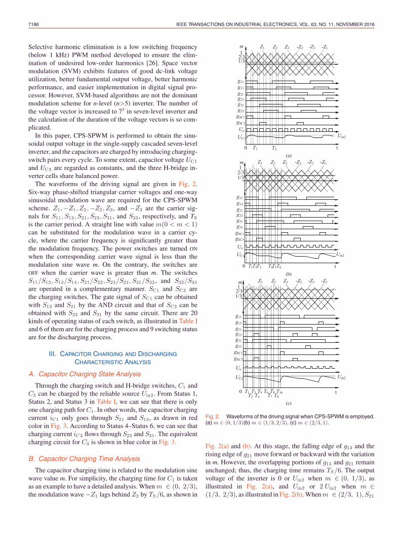
The waveforms of the driving signal are given in Fig. 2.Six-way phase-shifted triangular carrier voltages and one-waysinusoidal modulation wave are required for the CPS-SPWMscheme. Z1 ,−Z1 , Z2 ,−Z2 , Z3 , and −Z3 are the carrier sig-nals for S11 , S13 , S21 , S23 , S31 , and S33 , respectively, and TSis the carrier period. A straight line with value m(0 < m < 1)can be substituted for the modulation wave in a carrier cy-cle, where the carrier frequency is significantly greater thanthe modulation frequency. The power switches are turned ON
when the corresponding carrier wave signal is less than themodulation sine wave m. On the contrary, the switches areOFF when the carrier wave is greater than m. The switchesS11/S12 , S13/S14 , S21/S22 , S23/S24 , S31/S32 , and S33/S34are operated in a complementary manner. SC1 and SC3 arethe charging switches. The gate signal of SC1 can be obtainedwith S13 and S21 by the AND circuit and that of SC3 can beobtained with S23 and S31 by the same circuit. There are 20kinds of operating status of each switch, as illustrated in Table Iand 6 of them are for the charging process and 9 switching statusare for the discharging process.
III. CAPACITOR CHARGING AND DISCHARGING
CHARACTERISTIC ANALYSIS
A. Capacitor Charging State Analysis
Through the charging switch and H-bridge switches, C1 andC3 can be charged by the reliable source Uin2 . From Status 1,Status 2, and Status 3 in Table I, we can see that there is onlyone charging path for C1 . In other words, the capacitor chargingcurrent iC1 only goes through S21 and S13 , as drawn in redcolor in Fig. 3. According to Status 4–Status 6, we can see thatcharging current iC 3 flows through S23 and S31 . The equivalentcharging circuit for C3 is shown in blue color in Fig. 3.
B. Capacitor Charging Time Analysis
The capacitor charging time is related to the modulation sinewave value m. For simplicity, the charging time for C1 is takenas an example to have a detailed analysis. When m ∈ (0, 2/3),the modulation wave −Z1 lags behind Z2 by TS /6, as shown in
Fig. 2. Waveforms of the driving signal when CPS-SPWM is employed.(a) m ∈ (0, 1/3)(b) m ∈ (1/3, 2/3). (c) m ∈ (2/3, 1).
Fig. 2(a) and (b). At this stage, the falling edge of g13 and therising edge of g21 move forward or backward with the variationin m. However, the overlapping portions of g13 and g21 remainunchanged; thus, the charging time remains TS /6. The outputvoltage of the inverter is 0 or Uin2 when m ∈ (0, 1/3), asillustrated in Fig. 2(a), and Uin2 or 2 Uin2 when m ∈(1/3, 2/3), as illustrated in Fig. 2(b). When m ∈ (2/3, 1), S21
SUN et al.: SINGLE DC SOURCE CASCADED SEVEN-LEVEL INVERTER INTEGRATING SWITCHED-CAPACITOR TECHNIQUES 7187
TABLE IOPERATING STATUS OF EACH SWITCH
S1 1 S1 3 S2 1 S2 3 S3 1 S3 3 SC 1 SC 3
Charging status Status 1 1 1 1 0 0 0 1 0Status 2 1 1 1 1 0 0 1 0Status 3 1 1 1 0 1 0 1 0Status 4 0 0 1 1 1 0 0 1Status 5 0 0 1 1 1 1 0 1Status 6 1 0 1 1 1 0 0 1
Discharging status Status 7 1 0 0 0 1 1 0 0Status 8 1 0 1 1 0 0 0 0Status 9 1 0 1 0 1 1 0 0Status 10 1 0 1 0 0 0 0 0Status 11 1 0 0 0 1 0 0 0Status 12 1 0 1 1 1 0 0 0Status 13 1 0 1 0 1 0 0 0Status 14 1 1 0 0 1 0 0 0Status 15 0 0 1 0 1 0 0 0
Status 16 1 1 0 0 1 1 0 0Status 17 1 1 0 0 0 0 0 0Status 18 0 0 1 1 0 0 0 0Status 19 0 0 1 0 1 1 0 0Status 20 0 0 0 0 1 1 0 0
Fig. 3. Equivalent charging circuit for C1 and C3 .
TABLE IICHARGING TIME AND OUTPUT VOLTAGE IN DIFFERENT m
Modulation value m Charging time Output voltage
−1 < m < −2/3 (1− | m |)TS /2 −3U in2 , −2U in2 ,
−2/3 < m < −1/3 TS /6 −2U in2 , −U in2
−1/3 < m < 0 TS /6 −U in2 , 00 < m < 1/3 TS /6 0, −U in2
1/3 < m < 2/3 TS /6 U in2 , 2U in2
2/3 < m < 1 (1 − m )TS /2 2U in2 , 3U in2
is turned OFF after S13 , as illustrated in Fig. 2(c). The chargingtime is (1 − m)TS /2, and the output voltage of the inverter is2 Uin2 or 3 Uin2 and the capacitor voltage UC1 would decreasedrastically if the modulation wave is increased to 1; however, itwould recover in time if the modulation wave is decreased.
Due to the symmetry, the charging time and the output voltagecan be easily derived with m < 0. Table II gives the chargingtime and the output voltage in different m.
C. Capacitor Discharged Bus Voltage Analysis
To some extent, bus voltages UC1 and UC3 remain stable.However, they will fluctuate frequently because of the charging
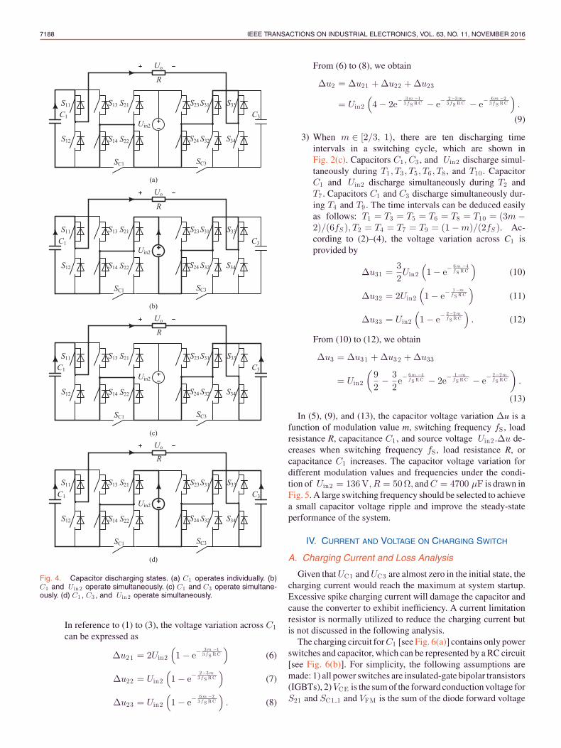
or discharging of the capacitor. The influencing factors of UC1and UC3 are illustrated as follows. For simplicity, the followingassumptions are made: 1) the initial values of UC1 and UC3 areUin2 before discharging; 2) the capacitance of the capacitor C1and C3 is C and the load resistance is R. There are four discharg-ing states for C1 in a modulation cycle, which are described asfollows.
State I: Capacitor C1 operates individually.S11 , S14 , S22 , S24 , S31 , and S33 are turned ON simultaneously
for Status 7 (S11 , S14 , S21 , S23 , S32 , and S34 are ON for Status8). The equivalent circuit of Status 7 is shown in Fig. 4(a). UC1can be expressed as
uC1(t) = Uin2e−t
R C . (1)
State II: Capacitor C1 and Uin2 operate simultaneously.S11 , S14 , S21 , S24 , S31 , and S33 are turned ON simultaneously
for Status 9 (S11 , S14 , S21 , S24 , S32 , and S34 are ON for Status10). The equivalent circuit of Status 9 is shown in Fig. 4(b). UC1is provided by
uC1(t) = Uin2(2e−t
R C − 1). (2)
State III: Capacitors C1 and C3 operate simultaneously.S11 , S14 , S22 , S24 , S31 , and S34 are turned ON simultaneously
for Status 11 (S11 , S14 , S21 , S23 , S31 , and S34 are ON for Status12). The equivalent circuit is shown in Fig. 4(c). UC1 can beexpressed as
uC1(t) = Uin2e−2 tR C . (3)
State IV: Capacitors C1 , C3 , and Uin2 operate simultane-ously.
S11 , S14 , S21 , S24 , S31 , and S34 are turned ON simultaneouslyfor Status 13. The equivalent circuit is shown in Fig. 4(d). UC1is provided by
uC1(t) = Uin2
(32e−
2 tR C − 1
2
). (4)
The analysis above reveals that the proposed converter hasfour discharging states. For convenience, the discharging timeintervals that belong to the same state are regarded as one con-tinuous discharging time.
1) When m ∈ [0, 1/3), there are two discharging timeintervals in a switching cycle, which are shown inFig. 2(a). The two time intervals can be deduced eas-ily as T1 = T2 = m/(2fS ). According to (1), the voltagevariation across C1 can be expressed as
Δu1 = Uin2 − Uin2e− m
f S R C . (5)
2) When m ∈ [1/3, 2/3) , there are six discharging timeintervals in a switching cycle, which are shown inFig. 2(b). Capacitor C1 and Uin2 discharge simulta-neously during T1 and T6 . Capacitor C1 dischargesindividually during T2 and T5 . Capacitors C1 and C3 dis-charge simultaneously during T3 and T4 . The time inter-vals can be achieved easily as follows: T1 = T3 = T4 =T6 = (3m − 1)/(6fS ), T2 = T5 = (2 − 3m)/(6fS ).
7188 IEEE TRANSACTIONS ON INDUSTRIAL ELECTRONICS, VOL. 63, NO. 11, NOVEMBER 2016
Fig. 4. Capacitor discharging states. (a) C1 operates individually. (b)C1 and Uin2 operate simultaneously. (c) C1 and C3 operate simultane-ously. (d) C1 , C3 , and Uin2 operate simultaneously.
In reference to (1) to (3), the voltage variation across C1can be expressed as
Δu21 = 2Uin2
(1 − e−
3 m −13 f S R C
)(6)
Δu22 = Uin2
(1 − e−
2−3 m3 f S R C
)(7)
Δu23 = Uin2
(1 − e−
6 m −23 f S R C
). (8)
From (6) to (8), we obtain
Δu2 = Δu21 + Δu22 + Δu23
= Uin2
(4 − 2e−
3 m −13 f S R C − e−
2−3 m3 f S R C − e−
6 m −23 f S R C
).
(9)
3) When m ∈ [2/3, 1), there are ten discharging timeintervals in a switching cycle, which are shown inFig. 2(c). Capacitors C1 , C3 , and Uin2 discharge simul-taneously during T1 , T3 , T5 , T6 , T8 , and T10 . CapacitorC1 and Uin2 discharge simultaneously during T2 andT7 . Capacitors C1 and C3 discharge simultaneously dur-ing T4 and T9 . The time intervals can be deduced easilyas follows: T1 = T3 = T5 = T6 = T8 = T10 = (3m −2)/(6fS ), T2 = T4 = T7 = T9 = (1 − m)/(2fS ). Ac-cording to (2)–(4), the voltage variation across C1 isprovided by
Δu31 =32Uin2
(1 − e−
6 m −4f S R C
)(10)
Δu32 = 2Uin2
(1 − e−
1−mf S R C
)(11)
Δu33 = Uin2
(1 − e−
2−2 mf S R C
). (12)
From (10) to (12), we obtain
Δu3 = Δu31 + Δu32 + Δu33
= Uin2
(92− 3
2e−
6 m −4f S R C − 2e−
1−mf S R C − e−
2−2 mf S R C
).
(13)
In (5), (9), and (13), the capacitor voltage variation Δu is afunction of modulation value m, switching frequency fS , loadresistance R, capacitance C1 , and source voltage Uin2 .Δu de-creases when switching frequency fS , load resistance R, orcapacitance C1 increases. The capacitor voltage variation fordifferent modulation values and frequencies under the condi-tion of Uin2 = 136V, R = 50Ω, and C = 4700 μF is drawn inFig. 5. A large switching frequency should be selected to achievea small capacitor voltage ripple and improve the steady-stateperformance of the system.
IV. CURRENT AND VOLTAGE ON CHARGING SWITCH
A. Charging Current and Loss Analysis
Given that UC1 and UC3 are almost zero in the initial state, thecharging current would reach the maximum at system startup.Excessive spike charging current will damage the capacitor andcause the converter to exhibit inefficiency. A current limitationresistor is normally utilized to reduce the charging current butis not discussed in the following analysis.
The charging circuit for C1 [see Fig. 6(a)] contains only powerswitches and capacitor, which can be represented by a RC circuit[see Fig. 6(b)]. For simplicity, the following assumptions aremade: 1) all power switches are insulated-gate bipolar transistors(IGBTs), 2) VCE is the sum of the forward conduction voltage forS21 and SC1 1 and VFM is the sum of the diode forward voltage

SUN et al.: SINGLE DC SOURCE CASCADED SEVEN-LEVEL INVERTER INTEGRATING SWITCHED-CAPACITOR TECHNIQUES 7189
Fig. 5. Scope of capacitor voltage variation at different modulationvalues and frequencies.
Fig. 6. Circuit and equivalent circuit of the charging process. (a) Charg-ing circuit. (b) Equivalent charging circuit.
Fig. 7. Capacitor voltage waveforms of charging process. (a) Fullcharging. (b) Partial charging.
for S13 and SC1 2 , and 3) RESR represents the equivalent seriesresistance (ESR) of the capacitor.
The capacitor voltage waveforms of charging process areillustrated in Fig. 7. VC1min denotes the initial capacitor volt-age and VC1max represents the final capacitor voltage. The ca-pacitor charging process can be classified into two conditions,namely, full charging and partial charging. In [24], full charging
is defined as one that has a charging time period longer thanfour times the charging time constant, i.e., Tch ≥ 4τch , and par-tial charging corresponds to Tch < 4τch , where τch = RESRC.In full charging, the capacitor is charged to the steady-statevoltage Uin2 − VCE − VFM , as shown in Fig. 7(a). In par-tial charging, the capacitor is charged to a voltage less thanUin2 − VCE − VFM , as shown in Fig. 7(b).
The instantaneous capacitor voltage and current can be givenby⎧⎨⎩
uC1(t) = VC1max + (VC1min − VC1max)e− t
R E S R C
iC1(t) = VC 1 m a x −VC 1 m inRE S R
e−t
R E S R C = ΔuRE S R
e−t
R E S R C
. (14)
The maximum charging current can be expressed by
iC1 max =Δumax
RESR. (15)
From Fig. 5, the capacitor voltage variation Δu is a functionof modulation value m at a certain switching frequency fS ,load resistance R, capacitance C, and source voltage Uin2 . Δuincreases when m increases.
Therefore, we get the peak current
iC1max =
Uin2
(92 − 3
2 e−6 m −4f S R C − 2e−
1−mf S R C − e−
2−2 mf S R C
)∣∣∣ m = mmax
RESR.
(16)
Charging loss can be expressed as follows:
Ploss =1TS
∫ Tch
0(i2C1(t)RESR+iC1(t)(VCE + VFM))dt
(17)where Tch is the charging time, for m ∈ (0, 2/3), Tch = TS/6,for m ∈ (2/3, 1), Tch = (1 − m)TS/2.
Substituting (14) into (17), we have
Ploss =fSCΔu2
2RESR
(1 − e−
2 T chR E S R C
)
+ fSCΔu(VCE + VFM)(
1 − e−T ch
R E S R C
). (18)
For a given m, the corresponding capacitor voltage can bededuced with (5), (9), and (13). Charging loss can be calculatedby (18). The charging loss for different modulation values andfrequencies under the condition of Uin2 = 136 V, R = 50Ωand C = 4700μF is drawn in Fig. 8. When the modulationvalue m becomes larger, the charging loss increases rapidlyat a small fS . But in general, with the increase of switchingfrequency, the switching loss will be greatly increased. Thus,the switching frequency fS can be chosen as more than 1.5 kHzto ensure a small capacitor voltage variation and charging lossacross the entire modulation index, as shown in Figs. 5 and 8. Inthis study, the switching frequency fS is selected as 1.667 kHzeventually so that the output voltage has a switching pattern with10 kHz.

7190 IEEE TRANSACTIONS ON INDUSTRIAL ELECTRONICS, VOL. 63, NO. 11, NOVEMBER 2016
Fig. 8. Extent of charging loss at different modulation amplitudes andfrequencies.
Fig. 9. Voltage of SC1 in state II.
B. Charging Switch Voltage Analysis
By introducing the charging-switch pairs, the proposed cas-caded seven-level inverter can operate well with only a singledc input source. It is necessary to analyze the charging-switchpair’s voltage stress and SC1 was taken as an example for thevoltage analysis. There are four voltage states for SC1 in a mod-ulation cycle, which are described as follows.
State I: S13 , S21 , and SC1 are turned ON. The positive sidesof C1 and Uin2 are connected directly. Input source Uin2 cancharge C1by introducing SC1 , as shown in Fig. 3. The voltageof SC1 is zero.
State II: S13 and S22 are turned ON, and SC1 is turned OFF.The voltage of SC1 is –SC1 , as shown in Fig. 9.
State III: In Fig. 4(b) and (d), S14 and S21 are turned ON, andthe voltage of SC1 is Uin2 .
State IV: In Fig. 4(a) and (c), S14 and S22 are turned ON andthe voltage of SC1 is zero.
States I–IV indicate that the voltage of SC1 is 0, the capacitorvoltage UC1 or the source voltage Uin2 . Therefore, the proposedconverter has low voltage stress on each switch, which resultedin low cost.
TABLE IIISYSTEM SIMULATION PARAMETERS
Circuit parameters Value
U in 2 136 Vfs 1.667 kHzR 50 ΩL 60 mHC1 /C3 4700 μF
Fig. 10. Output voltage and current waveforms. (a) At resistive load.(b) At inductive load. (c) THD value of the output voltage.
V. SIMULATION AND EXPERIMENTAL VERIFICATIONS
A. Simulation Results
The simulation parameters of the proposed converter aregiven in Table III.
SUN et al.: SINGLE DC SOURCE CASCADED SEVEN-LEVEL INVERTER INTEGRATING SWITCHED-CAPACITOR TECHNIQUES 7191
Fig. 11. Voltage waveforms of the charging-switch. (a) SC1 . (b) SC3 .
The output voltage and current waveforms for resistive andinductive load are given in Fig. 10. The output current lagsbehind the voltage at inductive load. And the current is smoothdue to the filter inductance. As shown in Fig. 10(c), the harmonicis mainly concentrated on the octave band and sidebands at10 kHz. The THD value of uO is 23.84%.
The ideal voltage waveforms of the charging-switch pairs SC1and SC3 are shown in Fig. 11. It can be seen that the voltagestates for SC1 and SC3 are 0, Uin2 or − Uin2 in a modulationcycle. The voltage stress of the charging-switch pair is withinthe source voltage, which verifies the theoretical analysis.
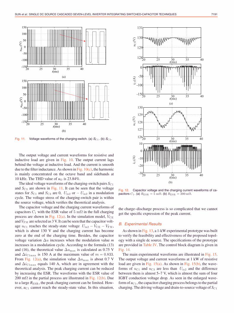
The capacitor voltage and the charging current waveforms ofcapacitors C1 with the ESR value of 5 mΩ in the full chargingprocess are shown in Fig. 12(a). In the simulation model, VCEand VFM are selected as 3 V. It can be seen that the capacitor volt-age uC1 reaches the steady-state voltage Uin2 − VCE − VFM ,which is about 130 V and the charging current has becomezero at the end of the charging time. Besides, the capacitorvoltage variation Δu increases when the modulation value mincreases in a modulation cycle. According to the formula (13)and (16), the theoretical value Δumax is calculated as 0.75 Vand ΔiC1max is 150 A at the maximum value of m = 0.833.From Fig. 12(a), the simulation value Δumax is about 0.7 Vand ΔiC1max equals 140 A, which are in agreement with thetheoretical analysis. The peak charging current can be reducedby increasing the ESR. The waveforms with the ESR value of200 mΩ in the partial process are illustrated in Fig. 12(b). Dueto a large RESR , the peak charging current can be limited. How-ever, uC1 cannot reach the steady-state value. In this situation,
Fig. 12. Capacitor voltage and the charging current waveforms of ca-pacitors C1 . (a) RESR = 5 mΩ. (b) RESR = 200 mΩ.
the charge–discharge process is so complicated that we cannotget the specific expression of the peak current.
B. Experimental Results
As shown in Fig. 13, a 1-kW experimental prototype was builtto verify the feasibility and effectiveness of the proposed topol-ogy with a single dc source. The specifications of the prototypeare provided in Table IV. The control block diagram is given inFig. 14.
The main experimental waveforms are illustrated in Fig. 15.The output voltage and current waveforms at 1 kW of resistiveload are given in Fig. 15(a). As shown in Fig. 15(b), the wave-forms of uC1 and uC3 are less than Uin2 and the differencebetween them is almost 5–7 V, which is almost the sum of fourIGBT conduction voltage drop. As seen in the enlarged wave-form of uC1 , the capacitor charging process belongs to the partialcharging. The driving voltage and drain-to-source voltage of SC1

7192 IEEE TRANSACTIONS ON INDUSTRIAL ELECTRONICS, VOL. 63, NO. 11, NOVEMBER 2016
Fig. 13. Prototype for the experiment.
TABLE IVUTILIZED COMPONENTS AND PARAMETERS
Components and parameters Value
Main control chip TMS320LF2407A + XC3S400Charging-switch pairs (IGBT) FGH40N60 (40 A, 600 V)Main switches (IGBT) FGH20N60 (20 A, 600 V)Capacitances C1 and C3 (μF) 4700Load voltage uorm s (V) 220 (PF = 1)Load side inductance L (mH) 60Output frequency fo (Hz) 50Switching frequency fS (kHz) 1.667Equivalent output switching frequency fE S (kHz) 10Modulation ratio 0.833
Fig. 14. Control block diagram of the single-supply cascaded seven-level inverter.
are shown in Fig. 15(c). The voltage across a charging-switchpair is within the source voltage. The output voltage and currentwaveform at inductive load are given in Fig. 15(d) and (e). Theexperimental results verify the feasibility and effectiveness ofthe proposed single-supply cascaded seven-level inverter.
The curves of efficiency versus power in the proposed andtraditional cascaded seven-level inverters with the same circuitparameters are illustrated in Fig. 16. The values of the twocurves are basically in agreement and both are more than 90%.However, the efficiency value of the proposed inverter is lowerthan that of the traditional inverter because of the charging loss.
Fig. 15. Experimental waveforms of the proposed inverter. (a) Outputvoltage and current at resistive load. (b) UC1 , UC3 and Uin2 . (c) Driv-ing voltage and drain-to-source voltage of SC1 . (d) Output voltage andcurrent at inductive load (PF = 0.9). (e) Output voltage and current atinductive load (PF = 0.68).

SUN et al.: SINGLE DC SOURCE CASCADED SEVEN-LEVEL INVERTER INTEGRATING SWITCHED-CAPACITOR TECHNIQUES 7193
Fig. 16. Efficiency versus power in the proposed and traditionaltopologies.
VI. CONCLUSION
A novel single dc source cascaded seven-level inverter in-tegrating switched-capacitor technique was developed in thispaper. In the proposed topology, the transformerless chargingcircuit only contains power switches and capacitors, and thecharging time is independent of the load. The operation prin-ciple and the charging–discharging characteristic analysis wereinvestigated in depth. With the common CPS-SPWM strategy,the sinusoidal output voltage can be well obtained. Moreover,the capacitors are properly charged without complex voltagebalancing control algorithm. The peak charging current and thecharging loss can be reduced with appropriate circuit parame-ters. The proposed topology has the features of modularity, lowcost, and simplicity of control and makes it attractive in dc–ac power applications. A 1-kW experimental prototype verifiesthe feasibility of the proposed inverter. The proposed inverteris also suitable for photovoltaic-battery multi-input applicationwith high redundancy.
REFERENCES
[1] S. Kouro et al., “Recent advances and industrial applications of multilevelconverters,” IEEE Trans. Ind. Electron., vol. 57, no. 8, pp. 2553–2580,Aug. 2010.
[2] H. Abu-Rub, J. Holtz, J. Rodriguez, and G. Baoming, “Medium-voltagemultilevel converters; state of the art, challenges, and requirementsin industrial applications,” IEEE Trans. Ind. Electron., vol. 57, no. 8,pp. 2581–2596, Aug. 2010.
[3] J. Dixon, J. Pereda, C. Castillo, and S. Bosch, “Asymmetrical multilevelinverter for traction drives using only one dc supply,” IEEE Trans. Veh.Technol., vol. 59, no. 8, pp. 3736–3743, Oct. 2010.
[4] S. Lu, K. A. Corzine, and M. Ferdowsi, “A unique ultracapacitor directintegration scheme in multilevel motor drives for large vehicle propulsion,”IEEE Trans. Veh. Technol., vol. 56, no. 4, pp. 1506–1515, Jul. 2007.
[5] J. Rodriguez, S. Bernet, P. K. Steimer, and I. E. Lizama, “A surveyon neutral-point-clamped inverters,” IEEE Trans. Ind. Electron., vol. 57,no. 7, pp. 2219–2230, Jul. 2010.
[6] M. Khazraei, H. Sepahvand, K. A. Corzine, and M. Ferdowsi, “Activecapacitor voltage balancing in single-phase flying capacitor multilevelpower converters,” IEEE Trans. Ind. Electron., vol. 59, no. 2, pp. 769–778, Feb. 2012.
[7] I. Ahmed and V. B. Borghate, “Simplified space vector modulation tech-nique for seven-level cascaded H-bridge inverter,” IET Power Electron.,vol. 7, no. 3, pp. 604–613, Apr. 2014.
[8] Y. H. Liao and C. M. Lai, “Newly-constructed simplified single-phasemulti-string multilevel inverter topology for distributed energy resources,”IEEE Trans. Power Electron., vol. 26, no. 9, pp. 2386–2391, Sep. 2011.
[9] L. Maharjan, S. Inoue, H. Akagi, and J. Asakura, “A transformerless bat-tery energy storage system based on a multilevel cascade PWM converter,”in Proc. 39th Annu. IEEE Power Electron. Conf., 2008, pp. 4798–4804.
[10] M. N. A. Kadir and Z. F. Hussien, “Asymmetrical multilevel inverter:Maximum resolution for H-bridge topology,” in Proc. Int. Conf. PowerElectron. Drivers Syst., 2005, pp. 1068–1071.
[11] M. Rotella, G. Penailillo, J. Pereda, and J. Dixon, “PWM method toeliminate power sources in a nonredundant 27-level inverter for machinedrive applications,” IEEE Trans. Ind. Electron., vol. 56, no. 1, pp. 194–201,Jan. 2009.
[12] J. Dixon, M. Ortuizar, R. Carmi, P. Barriuso, P. Flores, and L. Moran,“Static Var compensator and active power filter with power injection ca-pability, using 27-level inverters and photovoltaic cells,” in Proc. IEEEInt. Symp. Ind. Electron., 2006, pp. 1106–1111.
[13] J. Pereda and J. Dixon, “High-frequency link: A solution for using onlyone DC source in asymmetric cascaded multilevel inverters,” IEEE Trans.Ind. Electron., vol. 58, no. 9, pp. 3884–3892, Sep. 2011.
[14] J. Pereda and J. Dixon, “23-level inverter for electric vehicles using asingle battery pack and series active filters,” IEEE Trans. Veh. Technol.,vol. 61, no. 3, pp. 1043–1051, Mar. 2012.
[15] Z. Du, L. M. Tolbert, J. N. Chiasson, and B. Ozpineci, “A cascade mul-tilevel inverter using a single DC source,” in Proc. 21st Annu. IEEE Appl.Power Electron. Conf. Expo., 2006, pp. 426–430.
[16] D. U. Zhong, B. Ozpineci, L. M. Tolbert, and J. N. Chiasson, “DC-AC cascaded H-bridge multilevel boost inverter with no inductors forelectric/hybrid electric vehicle applications,” IEEE Trans. Ind. Appl., vol.45, no. 3, pp. 963–970, May/Jun. 2009.
[17] H. Sepahvand, J. Liao, and M. Ferdowsi, “Investigation on capacitor volt-age regulation in cascaded H-bridge multilevel converters with funda-mental frequency switching,” IEEE Trans. Ind. Electron., vol. 58, no. 11,pp. 5102–5111, Nov. 2011.
[18] H. Sepahvand, J. Liao, M. Ferdowsi, and K. A Corzine, “Capacitor voltageregulation in single-DC-source cascaded H-bridge multilevel convertersusing phase-shift modulation,” IEEE Trans. Ind. Electron., vol. 60, no. 9,pp. 3619–3626, Sep. 2013.
[19] S. Vazquez, J. I. Leon, L. G. Franquelo, J. J. Padilla, and J. M. Carrasco,“DC-voltage-ratio control strategy for multilevel cascaded converters fedwith a single DC source,” IEEE Trans. Ind. Electron., vol. 56, no. 7,pp. 2513–2521, Jul. 2009.
[20] M. D. Seeman and S. R. Sanders, “Analysis and optimization of switched-capacitor DC-DC converters,” IEEE Trans. Power Electron., vol. 23,no. 2, pp. 841–851, Mar. 2008.
[21] J. C. Mayo-Maldonado, J. C. Rosas-Caro, and P. Rapisarda, “Modelingapproaches for DC-DC converters with switched capacitors,” IEEE Trans.Ind. Electron., vol. 62, no. 2, pp. 953–959, Feb. 2015.
[22] M. Evzelman and S. Ben-Yaakov, “Average-current-based conductionlosses model of switched capacitor converters,” IEEE Trans. Power Elec-tron., vol. 28, no. 7, pp. 3341–3352, Jul. 2013.
[23] F. Zhang, L. Du, F. Z. Peng, and Z. Qian, “A new design method forhigh-power high-efficiency switched-capacitor dc–dc converters,” IEEETrans. Power Electron., vol. 23, no. 2, pp. 832–840, Mar. 2008.
[24] C.-K. Cheung, S.-C. Tan, C. Tse, and A. Ioinovici, “On energy efficiencyof switched-capacitor converters,” IEEE Trans. Power Electron., vol. 28,no. 2, pp. 862–876, Feb. 2013.
[25] J. C. Rosas-Caro1, J. C. Mayo-Maldonado, F. Mancilla-David, AValderrabano-Gonzalez, and F. Beltran Carbajal, “Single-inductor res-onant switched capacitor voltage multiplier with safe commutation,” IETPower Electron., vol. 8, no. 4, pp. 507–516, Apr. 2015.
[26] J. Rodriguez et al., “Multilevel converters: An enabling technology forhigh-power applications,” Proc. IEEE, vol. 97, no. 11, pp. 1786–1817,Nov. 2009.
Xiaofeng Sun (M’11) received the B.S. de-gree in electrical engineering from the North-east Heavy Machinery Institute, Heilongjiang,China, in 1993, and the M.S. and Ph.D. degreesin power electronics from Yanshan University,Qinhuangdao, China, in 1999 and 2005, respec-tively.
Since 2008, he has been a Professor withYanshan University, where he is also the Direc-tor of the Key Laboratory of Power Electronics forEnergy Conservation and Motor Drives of Hebei
Province, Qinhuangdao. From 2003 to 2007, he was an Associate Pro-fessor with Yanshan University. He has authored or coauthored morethan 70 journal and conference papers. His research interests includedc/dc converters, multiple-input converters, hybrid electric vehicles, mi-crogrids, and power quality control.

7194 IEEE TRANSACTIONS ON INDUSTRIAL ELECTRONICS, VOL. 63, NO. 11, NOVEMBER 2016
Baocheng Wang received the B.S. and M.S. de-grees in electrical engineering from the North-east Heavy Machinery Institute, Heilongjiang,China, in 1988 and 1991, respectively, andthe Ph.D. degree from Yanshan University, Qin-huangdao, China, in 2008.
Since 2005, he has been a Professor with theDepartment of Electrical Engineering, YanshanUniversity. His research interests include multi-level inverter technology, distributed generation,renewable energy, and fault diagnosis.
Yue Zhou received the B.S. and M.S. degrees inelectrical engineering from Yanshan University,Qinhuangdao, China, in 2012 and 2015, respec-tively.
She is currently an Assistant Experimental-ist in the Department of Electrical Engineering,Yanshan University. Her main research interestsinclude multiport dc–dc converters, switched-capacitor converters, and high-voltage-gain con-verters.
Wei Wang received the B.S. and M.S. degreesin electrical engineering from Yanshan Univer-sity, Qinhuangdao, China, in 2010 and 2013,respectively.
Since 2013, he has been a Motor Control En-gineer with the Medium-Voltage Converter R&DDepartment, Schneider, Beijing, China. His mainresearch interests include topology and con-trol of dc–dc converters and multilevel invertingtechnology.
Huiyuan Du received the B.S. and M.S. degreesin electrical engineering from Yanshan Univer-sity, Qinhuangdao, China, in 2008 and 2011,respectively.
He is currently a Software Engineerwith SANY Heavy Energy Machinery Co.,Ltd.,Beijing, China. His research interests includemultilevel inverting technology and wind powersystems.
Zhigang Lu received the B.S. degree in auto-matic control and the M.S. degree in systems en-gineering from Xi’an Jiaotong University, Xi’an,China, in 1985 and 1988, respectively, and thePh.D. degree in electric power systems and au-tomation from the North China Electric PowerUniversity, Beijing, China, in 1998.
He is the Dean of the School of ElectricalEngineering, Yanshan University, Qinhuangdao,China. His current research interests includeeconomic operation and control of power sys-
tems, power grid state estimation, power system planning, and nature-inspired optimization algorithms and their applications to various opti-mization problems.