74lcx138 low voltage 1-of-8 decoder/demultiplexerwith 5v
TRANSCRIPT

© 2004 Fairchild Semiconductor Corporation DS012417 www.fairchildsemi.com
March 1995
Revised February 2004
74LC
X138 L
ow
Vo
ltage 1-o
f-8 Deco
der/D
emu
ltiplexer w
ith 5V
Toleran
t Inp
uts
74LCX138 Low Voltage 1-of-8 Decoder/Demultiplexerwith 5V Tolerant Inputs
General DescriptionThe LCX138 is a high-speed 1-of-8 decoder/demultiplexer.This device is ideally suited for high-speed memory chipselect address decoding. The multiple input enables allowparallel expansion to a 1-of-24 decoder using just threeLCX138 devices or a 1-of-32 decoder using four LCX138devices and one inverter.
The 74LCX138 is fabricated with advanced CMOS technol-ogy to achieve high speed operation while maintainingCMOS low power dissipation.
Features 5V tolerant inputs
2.3V to 3.6V VCC specifications provided
6.0 ns tPD max (VCC = 3.3V), 10 µA ICC max
Power down high impedance inputs and outputs
±24 mA output drive (VCC = 3.0V)
Implements patented noise/EMI reduction circuitry
Latch-up performance exceeds 500 mA
ESD performance:
Human body model > 2000V
Machine model > 200V
Leadless DQFN package
Ordering Code:
Note 1: Devices also available in Tape and Reel. Specify by appending suffix letter “X” to the ordering code.
Note 2: DQFN package available in Tape and Reel only.
Order Number Package Number Package Description
74LCX138M(Note 1)
M16A 16-Lead Small Outline Integrated Circuit (SOIC), JEDEC MS-012, 0.150" Narrow
74LCX138SJ(Note 1)
M16D 16-Lead Small Outline Package (SOP), EIAJ TYPE II, 5.3mm Wide
74LCX138BQX(Note 2)
MLP016E 16-Terminal Depopulated Quad Very-Thin Flat Pack No Leads (DQFN), JEDEC MO-241, 2.5 x 3.5mm
74LCX138MTC(Note 1)
MTC16 16-Lead Thin Shrink Small Outline Package (TSSOP), JEDEC MO-153, 4.4mm Wide
www.fairchildsemi.com 2
74L
CX
138
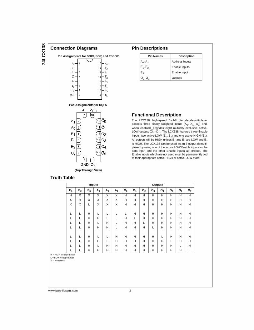
Connection Diagrams
Pin Assignments for SOIC, SOP, and TSSOP
Pad Assignments for DQFN
(Top Through View)
Pin Descriptions
Functional DescriptionThe LCX138 high-speed 1-of-8 decoder/demultiplexeraccepts three binary weighted inputs (A0, A1, A2) and,when enabled, provides eight mutually exclusive active-LOW outputs (O0–O7). The LCX138 features three Enableinputs, two active-LOW (E1, E2) and one active-HIGH (E3).All outputs will be HIGH unless E1 and E2 are LOW and E3
is HIGH. The LCX138 can be used as an 8-output demulti-plexer by using one of the active LOW Enable inputs as thedata input and the other Enable inputs as strobes. TheEnable inputs which are not used must be permanently tiedto their appropriate active-HIGH or active-LOW state.
Truth Table
H = HIGH Voltage LevelL = LOW Voltage LevelX = Immaterial
Pin Names Description
A0–A2 Address Inputs
E1–E2 Enable Inputs
E3 Enable Input
O0–O7 Outputs
Inputs Outputs
E1 E2 E3 A0 A1 A2 O0 O1 O2 O3 O4 O5 O6 O7
H X X X X X H H H H H H H H
X H X X X X H H H H H H H H
X X L X X X H H H H H H H H
L L H L L L L H H H H H H H
L L H H L L H L H H H H H H
L L H L H L H H L H H H H H
L L H H H L H H H L H H H H
L L H L L H H H H H L H H H
L L H H L H H H H H H L H H
L L H L H H H H H H H H L H
L L H H H H H H H H H H H L
3 www.fairchildsemi.com
74LC
X138
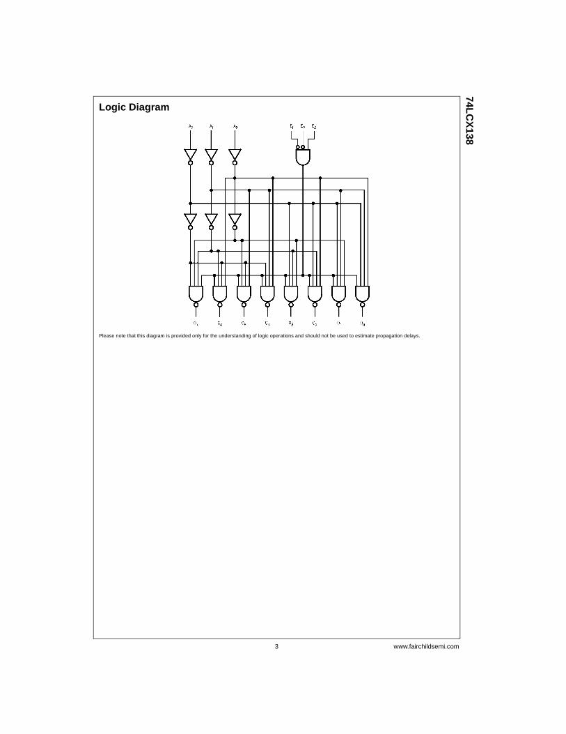
Logic Diagram
Please note that this diagram is provided only for the understanding of logic operations and should not be used to estimate propagation delays.
www.fairchildsemi.com 4
74L
CX
138
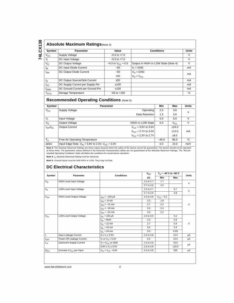
Absolute Maximum Ratings(Note 3)
Recommended Operating Conditions (Note 5)
Note 3: The Absolute Maximum Ratings are those values beyond which the safety of the device cannot be guaranteed. The device should not be operatedat these limits. The parametric values defined in the Electrical Characteristics tables are not guaranteed at the Absolute Maximum Ratings. The “Recom-mended Operating Conditions” table will define the conditions for actual device operation.
Note 4: IO Absolute Maximum Rating must be observed.
Note 5: Unused inputs must be held HIGH or LOW. They may not float.
DC Electrical Characteristics
Symbol Parameter Value Conditions Units
VCC Supply Voltage −0.5 to +7.0 V
VI DC Input Voltage −0.5 to +7.0 V
VO DC Output Voltage −0.5 to VCC + 0.5 Output in HIGH or LOW State (Note 4) V
IIK DC Input Diode Current −50 VI < GND mA
IOK DC Output Diode Current −50 VO < GNDmA
+50 VO > VCC
IO DC Output Source/Sink Current ±50 mA
ICC DC Supply Current per Supply Pin ±100 mA
IGND DC Ground Current per Ground Pin ±100 mA
TSTG Storage Temperature −65 to +150 °C
Symbol Parameter Min Max Units
VCC Supply Voltage Operating 2.0 3.6V
Data Retention 1.5 3.6
VI Input Voltage 0.0 5.5 V
VO Output Voltage HIGH or LOW State 0.0 VCC V
IOH/IOL Output Current VCC = 3.0V to 3.6V ±24.0
mAVCC = 2.7V to 3.0V ±12.0
VCC = 2.3V to 2.7V ±8.0
TA Free-Air Operating Temperature −40.0 85.0 °C∆t/∆V Input Edge Rate, VIN = 0.8V to 2.0V, VCC = 3.0V 0.0 10.0 ns/V
Symbol Parameter ConditionsVCC TA = −40°C to +85°C
Units(V) Min Max
VIH HIGH Level Input Voltage 2.3 to 2.7 1.7V
2.7 to 3.6 2.0
VIL LOW Level Input Voltage 2.3 to 2.7 0.7V
2.7 to 3.6 0.8
VOH HIGH Level Output Voltage IOH = −100 µA 2.3 to 3.6 VCC − 0.2
V
IOH = -8 mA 2.3 1.8
IOH = −12 mA 2.7 2.2
IOH = −18 mA 3.0 2.4
IOH = −24 mA 3.0 2.2
VOL LOW Level Output Voltage IOL = 100 µA 2.3 to 3.6 0.2
V
IOL = 8mA 2.3 0.6
IOL = 12 mA 2.7 0.4
IOL = 16 mA 3.0 0.4
IOL = 24 mA 3.0 0.55
II Input Leakage Current 0 ≤ VI ≤ 5.5V 2.3 to 3.6 ±5.0 µA
IOFF Power-Off Leakage Current VI or VO = 5.5V 0.0 10.0 µA
ICC Quiescent Supply Current VI = VCC or GND 2.3 to 3.6 10.0µA
3.6V ≤ VI ≤ 5.5V 2.3 to 3.6 ±10.0
∆ICC Increase in ICC per Input VIH = VCC −0.6V 2.3 to 3.6 500 µA
5 www.fairchildsemi.com
74LC
X138
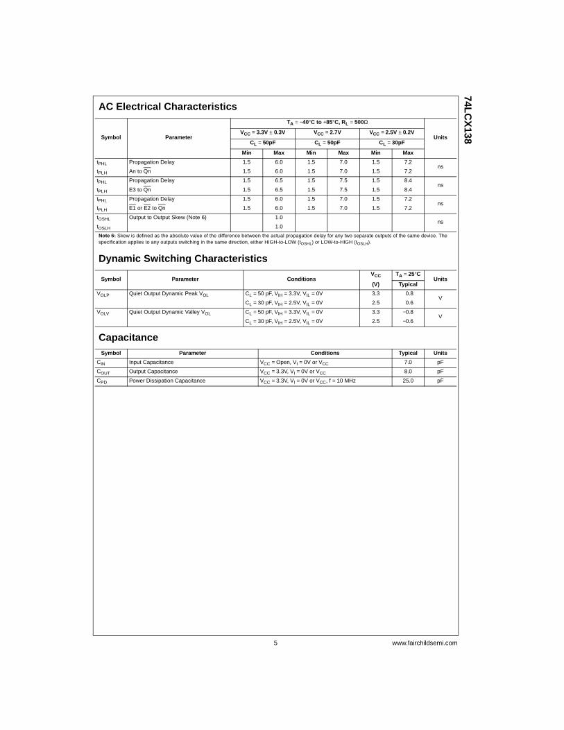
AC Electrical Characteristics
Note 6: Skew is defined as the absolute value of the difference between the actual propagation delay for any two separate outputs of the same device. Thespecification applies to any outputs switching in the same direction, either HIGH-to-LOW (tOSHL) or LOW-to-HIGH (tOSLH).
Dynamic Switching Characteristics
Capacitance
Symbol Parameter
TA = −40°C to +85°C, RL = 500Ω
UnitsVCC = 3.3V ± 0.3V VCC = 2.7V VCC = 2.5V ± 0.2V
CL = 50pF CL = 50pF CL = 30pF
Min Max Min Max Min Max
tPHL Propagation Delay 1.5 6.0 1.5 7.0 1.5 7.2ns
tPLH An to Qn 1.5 6.0 1.5 7.0 1.5 7.2
tPHL Propagation Delay 1.5 6.5 1.5 7.5 1.5 8.4ns
tPLH E3 to Qn 1.5 6.5 1.5 7.5 1.5 8.4
tPHL Propagation Delay 1.5 6.0 1.5 7.0 1.5 7.2ns
tPLH E1 or E2 to Qn 1.5 6.0 1.5 7.0 1.5 7.2
tOSHL Output to Output Skew (Note 6) 1.0ns
tOSLH 1.0
Symbol Parameter ConditionsVCC TA = 25°C
Units(V) Typical
VOLP Quiet Output Dynamic Peak VOL CL = 50 pF, VIH = 3.3V, VIL = 0V 3.3 0.8V
CL = 30 pF, VIH = 2.5V, VIL = 0V 2.5 0.6
VOLV Quiet Output Dynamic Valley VOL CL = 50 pF, VIH = 3.3V, VIL = 0V 3.3 −0.8V
CL = 30 pF, VIH = 2.5V, VIL = 0V 2.5 −0.6
Symbol Parameter Conditions Typical Units
CIN Input Capacitance VCC = Open, VI = 0V or VCC 7.0 pF
COUT Output Capacitance VCC = 3.3V, VI = 0V or VCC 8.0 pF
CPD Power Dissipation Capacitance VCC = 3.3V, VI = 0V or VCC, f = 10 MHz 25.0 pF

www.fairchildsemi.com 6
74L
CX
138
AC Loading and Waveforms Generic for LCX Family
FIGURE 1. AC Test Circuit
(CL includes probe and jig capacitance)
Waveform for Inverting and Non-Inverting Functions
Propagation Delay, Pulse Width and trec Waveforms
3-STATE Output High Enable and Disable Times for Logic
3-STATE Output Low Enable andDisable Times for Logic
Setup Time, Hold TIme and Recovery TIme for Logic
trise and tfall
FIGURE 2. Waveforms
(Input Pulse Characteristics; f = 1MHz, tr = tf = 3ns)
Test Switch
tPLH, tPHL Open
tPZL, tPLZ 6V at VCC = 3.3V ± 0.3V
VCC x 2 at VCC = 2.5V ± 0.2V
tPZH, tPHZ GND
SymbolVCC
3.3V ± 0.3V 2.7V 2.5V ± 0.2V
Vmi 1.5V 1.5V VCC/2
Vmo 1.5V 1.5V VCC/2
Vx VOL + 0.3V VOL + 0.3V VOL + 0.15V
Vy VOH − 0.3V VOH − 0.3V VOH − 0.15V

7 www.fairchildsemi.com
74LC
X138
Schematic Diagram Generic for LCX Family

www.fairchildsemi.com 8
74L
CX
138
Tape and Reel SpecificationTape Format for DQFN
TAPE DIMENSIONS inches (millimeters)
REEL DIMENSIONS inches (millimeters)
Package Tape Number Cavity Cover Tape
Designator Section Cavities Status Status
Leader (Start End) 125 (typ) Empty Sealed
BQX Carrier 3000 Filled Sealed
Trailer (Hub End) 75 (typ) Empty Sealed
Tape Size A B C D N W1 W2
12 mm13.0 0.059 0.512 0.795 2.165 0.488 0.724
(330.0) (1.50) (13.00) (20.20) (55.00) (12.4) (18.4)

9 www.fairchildsemi.com
74LC
X138
Physical Dimensions inches (millimeters) unless otherwise noted
16-Lead Small Outline Integrated Circuit (SOIC), JEDEC MS-012, 0.150" NarrowPackage Number M16A

www.fairchildsemi.com 10
74L
CX
138
Physical Dimensions inches (millimeters) unless otherwise noted (Continued)
16-Lead Small Outline Package (SOP), EIAJ TYPE II, 5.3mm WidePackage Number M16D

11 www.fairchildsemi.com
74LC
X138
Physical Dimensions inches (millimeters) unless otherwise noted (Continued)
16-Terminal Depopulated Quad Very-Thin Flat Pack No Leads (DQFN), JEDEC MO-241, 2.5 x 3.5mmPackage Number MLP016E

www.fairchildsemi.com 12
74L
CX
138
Lo
w V
olt
age
1-o
f-8
Dec
od
er/D
emu
ltip
lexe
r w
ith
5V
To
lera
nt
Inp
uts Physical Dimensions inches (millimeters) unless otherwise noted (Continued)
16-Lead Thin Shrink Small Outline Package (TSSOP), JEDEC MO-153, 4.4mm WidePackage Number MTC16
Fairchild does not assume any responsibility for use of any circuitry described, no circuit patent licenses are implied andFairchild reserves the right at any time without notice to change said circuitry and specifications.
LIFE SUPPORT POLICY
FAIRCHILD’S PRODUCTS ARE NOT AUTHORIZED FOR USE AS CRITICAL COMPONENTS IN LIFE SUPPORTDEVICES OR SYSTEMS WITHOUT THE EXPRESS WRITTEN APPROVAL OF THE PRESIDENT OF FAIRCHILDSEMICONDUCTOR CORPORATION. As used herein:
1. Life support devices or systems are devices or systemswhich, (a) are intended for surgical implant into thebody, or (b) support or sustain life, and (c) whose failureto perform when properly used in accordance withinstructions for use provided in the labeling, can be rea-sonably expected to result in a significant injury to theuser.
2. A critical component in any component of a life supportdevice or system whose failure to perform can be rea-sonably expected to cause the failure of the life supportdevice or system, or to affect its safety or effectiveness.
www.fairchildsemi.com