78 0o6;i07
TRANSCRIPT
LLJ -
for ublic reccd sc~ sdistribution is uhrl ted,
UNITED STATES AIR FORCEAIR UNIVERSITY
AIR FORCE INSTITUTE OF TECHNOLOGYWright-Patterson Air F'orce Base,Ohio
78 0O6;i07

GEO/PH/77-4 6
This document has been apnrfor public relcase aid salo; ii -"
distribution is unlimited.
DIFFERENTIAL-HALL IMPURITY
uPROFILING OF GaAs, CO-IMPLANTED
Co WITH Ga+, C+ AND As+, C+
THESIS
GEO/P/77-4 Michael Stefiniw2Lt USAF
Approved for public release; distribution unlimited
78 6'j5 EV•y
DIFFERENTIAL-HALL IMPURIYPOIIGO~atC+ A + , +.1O-I.MPLANTED WITH Ga+ , CAND A
Presented to the Faculty of the School of Engineering
of the Air Force Institute of Technology
Air University
in Partial Fulfilment of the
Requirements for the Degree of
Master of Science
by
ci Mchae Stefi n iwB. E.
2Lt USAF
Graduate El ectro-Optics
Approved for public release; distribution unlimited
I "
Preface
[ From the start, this thesis has been most interesting and informative.
It was most rewarding to do this thesis for two reasons. First, not much
research has been done in dual implantations, and secondly, the results
obtained suggest the possibilities which this field of work offers.
Future work should be carried out on the carbon-ion for it shows the
possibility of a useful dopant for submicron devices, since the diffusion
is negligible up to annealing temperatures of 900C.
I wish to thank the people who made this project possible for me.,!
I would particularly like to thank Jim Ehret who implanted my samples,
Charles Geesner for capping my samples as quickly as possible and
Captain David Lank for letting me use his computer profiling program
and Bok Kyoon Shin who was my lab advisor and gave me many suggestions.
Additional thanks go to my project sponsor Yoon Soo Park and faculty
advisor Dr. T. Luke.
1SslilforODC White sectionU~OU Butt Section
iiBy" RIB NYAPY, * ,,,
Table of Contents
Preface . . . , . . . . . . , . .. . ., . it
List of Figures . . . . . . . . . . . . . . . . . . . . . . . . iv
List of Tables . . . . . .. . .. . . . . . . . .. . vi
Abstract . . . . . . . . . . . . . ... . . . . . . vii
1. Introduction . . . . . . . . . . . . . . . . . . . . . . 1
Statement of Problem . . . . . . . . . . . . . . . ... 2Summary of Current Knowledge . . . . . . . . . . . . . . 2Theory . . . . . . . . . . . . . . . . .Scope . . . . . . .. .. . ., . .. . 4
I. Experimental Procedure . . . . . . . . . . 5
Sample Preparation . a . ..a. .a a . .. . . . ... 5Implantation Procedure . . a . . . a . a . . . . . . . . 6Encapsulation and Annealing . . . ... . . . a .. .. 7Data Aquisition and Processing . . . . . a . . . . . . 11
Il1. Experimental Results . . . . a . a a a . . . a a . . . 18
Isochronal Annealing .............. ... 18GaAs:C+ , .+ . a . . .a a a a . a . 18GaAs:a C 24GaAs :AsT, C .. . .. . . . 27
GaAs:Ar. .. . . . . . . a 30Electrical Profiles . .. ". . a a : . a a a : . . 31
IV. Discussion of Experimental Results . .. .. . . . . . . 37
V. Summary, Conclusion and Recommendations . . .. .. . . 41
Bibliography . ..a. . . . . . . . . . . . . . . . . . . . . . 43
Appendix A . . a a a a . a . . . a a . . a . a a a a a a a 44
Appendix B . . . . . . . . . . . . . . . . . . . . . . . . . 45
Appendix C .. a a . a a a a .a . . 46
Appendix D . t . . , a a q a 47
Appendix E . a a . . a a a a 49
Appendix F .. . . . . . . 52
Vita .. . . . .a . a a . a . a a a a 54
iii
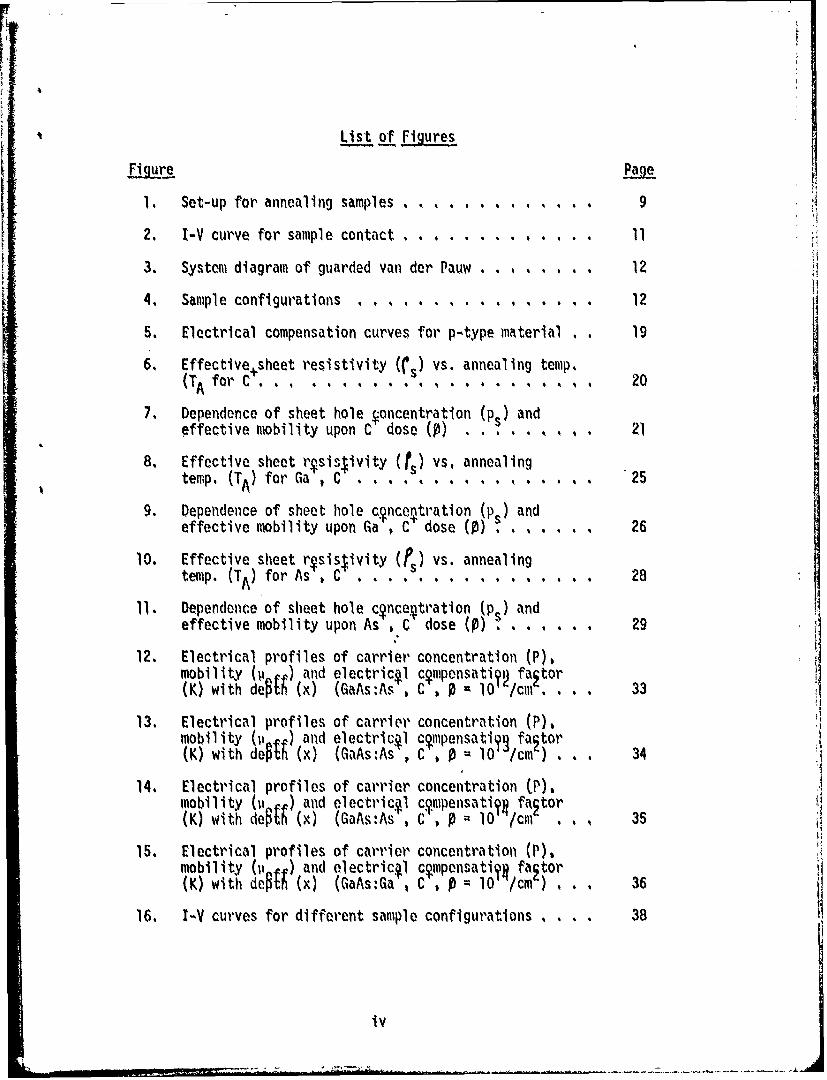
List of Figures
1. Set-up for annealing samples . . , .. . 9
2, I-V curve for sample contact . . . . . . . . . . 11
3. System diagram of guarded van der Pauw . , .. . 12
4. Sample configurations .. ... , . . .... 12
5. Electrical compensation curves for p-type material , . 19
6. Effective sheet resistivity (C5) vs. annealing temp.
(TA for C + . , . . . . . . 0 4 , . , , , 20
7. Dependence of sheet hole oncentration (ps) andeffective mobility upon C dose (J) ... . , 21
8. Effective sheet rsisJivity (ts) vs, annealingtemp. (T A) for Ga'-, C". . . .. .. . . . "25
9. Dependence of sheet hole cqncentration (p ) andeffective mobility upon Ga , C' dose (0) . , . , 26
10. Effective sheet rvsislivity (P5) vs. annealingtemp. (TA) for As , C . .. .. . . 28
11. Dependence of sheet hole cqncetration (p.) andeffective mobility upon As , C dose (0) . . . . 29
12. Electrical profiles of carrier concentration (P),mobility (P ) and electricql c~mpensati?2 fator(K) with deF[9 () (GaAs:As , , 10 /cm . . . . 33
13. Electrical profiles of carrier concentration (P),mobility (11 ) and electricql c~mpensatiQj factor(K) with de$U (x) (GaAs:As ,C, 0 -10 /cm ) . . , 34
14. Electrical profiles of carrier concentration (P),mobility ( ) and electrical cqmpensatin fator(K) with deF19 (x) (GaAs:As , C , j 1 /cm , 35
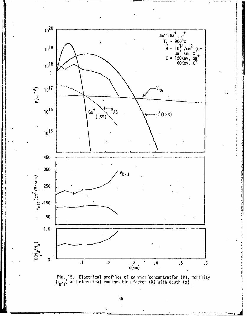
15. Electrical profiles of carrier concentration (P),mobility (it ) and electricql c~mpensatin fator(K) with deU$ (x) (GaAs:Ga , C , P 10 /cm ) , . , 36
16. I-V curves for different sample configurations . ... 38
il
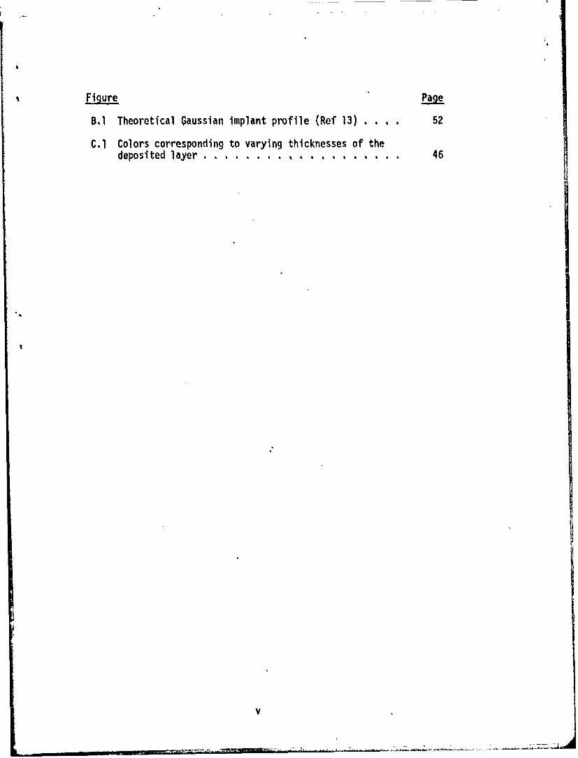
44
B.I Theoretical gaussian implant profile (Ref 13) . . . . 52
C.1 Colors corresponding to varying thicknesses of thedeposited layer . ... . . 46
tv
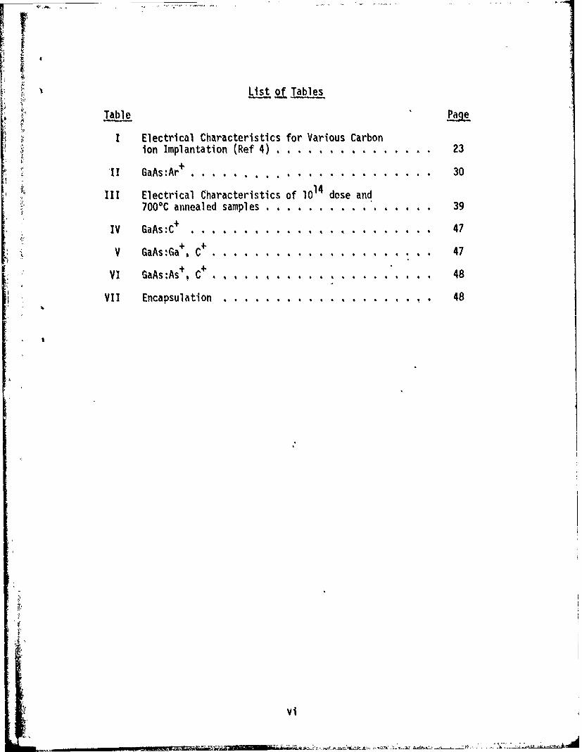
List oTables
Table e
I Electrical Characteristics for Various Carbon
ion Implantation (Ref 4) . . . . . . . . . .... . 23
'II GaAs:Ar+ 30
III Electrical Characteristics of l14 dose and7000C annealed samples ................ 39
IV GaAs: C+ ...... . .... 47
V GaAs:Ga+ C 47
VI GaAs:As+ C . ,. . . .. . . . .... 48
VII Encapsulation . 48
-vi
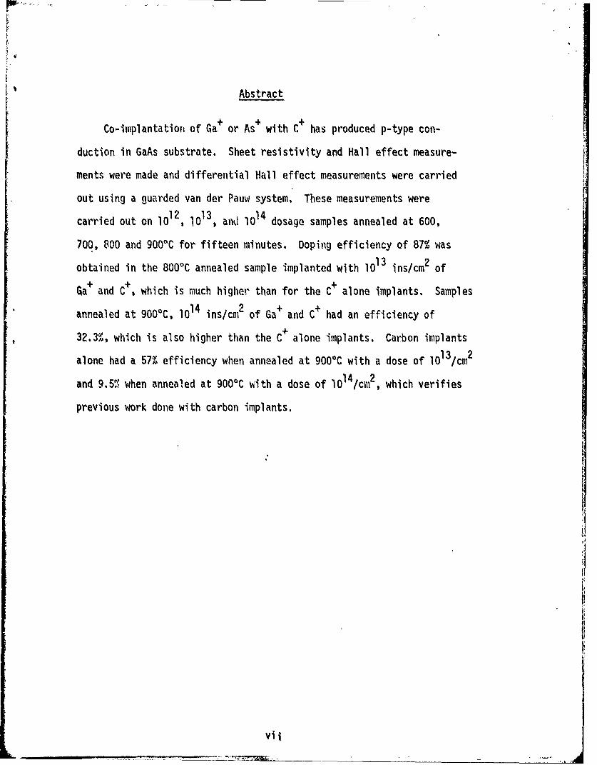
Abstract
Co-implantatiorn of Ga+ or As+ with C+ has produced p-type con-
duction in GaAs substrate. Sheet resistivity and Hall effect measure-
ments were made and differential Hall effect measurements were carried
out using a guarded van der Pauw system. These measurements were
carried out on 1012, 10 13 and 1014 dosage samples annealed at 600,
700, 800 and 900% for fifteen minutes. Doping efficiency of 87% was
obtained in the 8000C annealed sample implanted with 1013 ins/cm 2 of
Ua+ and C+ , which is much higher than for the C+ alone implants. Samples
annealed at 9000C, 1014 ins/cm2 of Ga+ and C+ had an efficiency of
32.3%, which is also higher than the C+ alone implants. Carbon implants
alone had a 57% efficiency when annealed at 9000C with a dose of 1O13/cm2
and 9.50 when annealed at 900C with a dose of lo4/cm2, which verifies
previous work done with carbon implants.
ii
vii
I. Introduction
The need for devices such as laser diodes, microwave components,
integrated optics, and digital IC's with multigigabit data rates has
prompted research in the ion implantation field of semiconductor fabri-
cation. The reason for using ion implantation and why so much time and
effort is being placed on it, is that the doping densities, distribution
and layer thickness are thought to be controlled more precisely than
d ffusion or epitaxial growth.
n implantation is a relatively new method of doping GaAs semi-
conductors but has been successfully used in devices with silicon
substrates. It is a process by which impurity ions are accelerated by
a particle accelerator and implanted into the substrate. The depth to Iwhich the impurity ions will penetrate is dependent upon the Ion mass,
energy of the beam and crystal orientation. After the implantation
crystal lattice damage exists which must be annealed by heat treatment.
This process is also used to electrically activate the impurity ions
for conduction by moving them into the crystal sites. However, the
annealing temperature required to effectively do the job exceeds the
temperature where the GaAs surface begins to decompose. To prevent or
reduce this effect the sample is encapsulated by a dielectric layer of
SiN , approximately 00 thick. This layer is placed on the sample
after implantation and belore annealing. The dielectric layer is
etched away when alectriqal measurements are performed on the sample.
The guarded van der Pau\ measuring system is used to acquire the crystal
and Hal oltages of th samples. Electrical profiles are obtained on fthe 90O annealed sampilos by a successive etching technique.
gj
Statement of Problem
There has been very little research done in the area of carbon ion
implanted gallium arsenide. The research that has been performed has
produced results demonstrating that p-type layers can be produced in
ion implanted samples. There has been no research investigating the
possibility of forming an n-type layer in GaAs with carbon.
The problem to be examined in this thesis is that of forming an
n-type layer in GaAs, by co-implantation of carbon ions with arsenic
incoporation. The possibility of increasing the electrical activity of
the carbon ions in p-type material by co-implantation with gallium is
also examined. The former objective is worth the time to investigate
because experimentation has shown that the group IV impurity atom tendIto replace the larger of the two-sub-lattice atoms which form the com-pound (Ref 2:70). This would have technological value in that submicron
devices of both n- or p-type layers could be formed by doping with
K icarbon ions and controlling the GaAs stoicheometry by either Ga or As co-
implantation.
Summary of Current Knowledge
INo work has specifically been done in obtaining an n-type layer in
GaAs using carbon ion implantation. However, all group IV elements have
been successfully used in forming n-type layers, with the exception of
carbon. Previously, some work was done in p-type layer implants using
* -carbon but the doping efficiencies were so low that it was believed
carbon might be useless as an impurity for ion implantation. Some
research done recently along these lines has been concerned with obtain-
ing p-type layer in GaAs using carbon ion implantation (Ref 4). The
2

results were a great improvement over previous work, in some cases,
doping efficiencies (n=Ps/f) of 50% were obtained, compared with previous
efficiencies of 7%. Co-implantation has'been shown to enhance donor and
acceptor activity in selenium and silicon implants (Ref 5,6). The
problems encountered are complex but the potential of this technique
warrants work in this area.
Theory
The theory behind the work performed here was developed by Hecking-
bottom and Ambridge for binary compound semiconductors such as gallium
arsenide (Ref 1). The reason such a theory was developed stemmed from
the great difference in implanting into a element such as silicon and
binary compounds. The model to represent the doping of silicon is as
follows, using Kroger-Vink notation (see Appendix A):F(g) ± Fsi (x)
Fsi Xr FSi + h (2)
The situation is much simpler here due to the fact that there is only
one sub-lattice to build up. When an dopant is implanted in the binary
compound case, only one sub-lattice is built and a compensating defect
is formed (Ref 1). The situation can be described as follows:
F(g) FAsx + V GAX (3)
V xN i + h" (4)~GA GA +h
which disrupts GaAs stoicheometry. The method of controlling this non-
stoicheometry is to implant an equal amount of the host atom on the
other sublattice when the dopant is being implanted.
3
This is only part of the sublattice control which must be done.
Time dependent non-stoicheometry arises during the annealing process.
The encapsulation process is used to combat this out-diffusion.
Scope
The work performed is limited to electrical measurements and pro-
filing using the van der Pauw system. Due to the time involved, surface
measurements were taken for all the samples while only five profiles
were completed. This gave some insight to the processes taking place
but is in no way complete. Glow Discharge Optical Spectroscopy which
would give a spatial distribution of the total impurity, was not done,
due to the lack of equipment accessibility. Two such profiles, one
obtained electrically and the other obtained optically, could be compared
and correlated. This would give us a better understanding of the
distribution of impurity ions that are used in this study.
In the following chapter, the various sections discuss sample
preparation, implantation, annealing, encapsulation, differential Hall
technique, and data processing. The results are presented in graphical
form so that the trends of the implants can be visualized. Following
this chapter, a discussion is presented on what is believed to be
happening, and why. A summary, conclusion and recommendation section
makes up the final portion of this study.
4
II. Expeimental Procedure
This chapter on experimental procedure will be made up of several
subsections. The sections will be covered in the following order:
sample preparation, implantation procedure, encapsulation and annealing
process, data acquisition and processing and finally equipment listViand figure of set-up.
The gallium arsenide used in this experiment was obtained from
Laser Diodes Laboratories and ordered chromium doped to make it semi-
insulating. Three wafers were used approximately 2 1/2 inches in
diameter and 20 mils thick. They were all from the same boule, two
wafers heing next to each other, while the third was from a different
part of the same boule. The samples have a resistivity of l0 9 ohms and
a chromium concentration of vlol,/cm3 as measured by mass-spectroscopic
analysis technique.
Sample Preparation
The wafers were cut into twenty-five samples, 5ini square making
maximum use of the wafer. A wafer scriber was used to cut the wafers,
holding them in place by a vacuum chuck. This size was found to be the
best to handle and made implanting much easier. The reason for this is
that four samples could be implanted at the same time with the same
dose.
The samples were then cleaned to remove any organic substance or
film which might have been present on the polished surface. The sample
was placed in a solution of aquasol concentrate and water in a ratio of
10:1 by volume. This soap solution, in a beaker was placed in an ultra-
sonic cleaner containing water filled to the same height as the soap
5-. - - - -- - - - - - - - - - - - - -- .
I' *1
solution in the beaker. The sample was then allowed to clean for five
minutes. After cleaning in the soap solution, the sample was rinsed with
deionized water for one minute to completely remove the soap. Then
the sample was rinsed with the following solvents: trichlorethylene(.CL2C:CICL) for twenty seconds, acetone (CH COCH 3) for twenty seconds
3) for twenty 33conds
and finally methanol (CH3OH) for twenty seconds, in that order. The
sample was then blown dry by a spray of purified nitrogen gas. The
surface was then checked for'any organic residue and surface oxidation
by dark field microscopy. If either of these were found not to be
removed by the above procedure, the cleaning process was repeated until
all the residue and oxidation was gone. When the surface is clean of
residue, the free etch (described next) was used to clean and remove
any mechanical damage which might be present. (This is necessary for
coherent adhesion of the capping material.) The free etch is composed
of the following chemical mixtures: H 20:30% H202:H2S04 in a volume
ratio of 1:1:5. The chip was placed in the etch for one minute while
being constantly agitated. This is'done so that pits or surface
deterioratiop will not occur. When removed from the etch the sample
was immediatcly rinsed with deionized water for one minute to remove
any acid from the surface and blown dry with an inert gas. After the
above procedure is accomplished the chip was placed in the ion implantation
facility to protect it from the formation of oxides or organic residue
on the surface.
Implantation Procedure
The 150Kev ion accelerator used in the following work was an
Accelerator Inc., Modified Implanter-I, which has been highly modified
6
for the work being done at the Air Force Avionics Laboratory (AFAL). The
machine-has two means of generating ions for implantation: either a hot-
cathode source or a radio frequency discharge. The hot-cathode source
is used to ionize solid materials, while the radio frequency (RF) dis-
charge is used for ionizing gases. In the present investigation, both
sources were used to obtain the ions for implantation. The samples
which were implanted with carbon ions (C+) only used the RF discharge
to obtain C+ from carbon dioxide (C02) gas. The samples which had dual
implants had to use both sources. The first batch of dual implant
samples were implanted with arsenic, obtained from arsenic metal, and
with carbon, in equal dosage. The second batch of dual implants were
implanted first with gallium obtained from gallium triflouride and with
carbon, also in equal dosage. Three doping concentrations (1012/cm2,
1013/cm 2 and l01 4 /cm2 ) were used for each of the three types of materials
(GaAs: C+, GaAs: As+ , C+ and GaAs: Ga+, C+) making nine different types
of samples i' all. The energy of the implants were 60Kev for the C+
and 120Kev for the gallium and arsehic ions. These were not the
energies which were desired to implant the ions but they were only what
the acceleratur could handle. It would have been preferred to implant
the carbon ion at 120Kev and gallium and arsenic ions at 700Kev, so
that the two distributions of implants would overlap more completely
and minimize surface erosion during implantation. The energies used
did show some overlapping of distributions, but not as much as was
desired.
Encapsulation and Annealing Conditions
After the implantation of the ions, the samples were encapsulated
7
with silicon nitride (Si3N4) a material which has been well documented
in the literature to be superior to silicon dioxide (Si0 2) for GaAs
encapsulation((Ref 4). The cap was used in this thesis to prevent
gallium from out-diffusing, which occurs at temperatures of 600C
(Ref 4).0
All the samples were coated with approximately lO00A of Si3N4, as
determined by the color change'which takes place on the surface of the
sample during the encapsulation process (Appendix C). This cap can
also be placed on the surface prior to implantation so as to control
the position and shape of the distribution.
The pyrolytic reactor used in this thesis for encapsulation was
designed based on a MIT Lincoln Laboratories set-up (.Ref 3:26). It is
possible to encapsulate samples with two different types of films using
this system, SiO 2 or Si3N4 . For this experiment, Si3N4 film was de-
posited on the sample by using specific amounts of nitrogen (N2),
ammonia (NH3) and silane (SiH 4) mixed in a glass bell chamber. The
chamber was first evacuated to remoVe impurities from the system, after
which it was purged with nitrogen. The sample rested on a carbon strip
whose temperature was controlled, thus allowing the reaction which is
necessary for the deposition of the film. As the chamber was being
purged with nitrogen, the sample was brought to 2000C, helping to pre-
vent any silicon dioxide from forming on the surface. Formation of
silicon dioxide would prevent coherent adhesion of the Si N film. After
purging for a few minutes, controlled amounts of 5% saline and liquid
anmonia were introduced which had been previously diluted with equal
amounts of nitrogen, These mixtures were added to the chamber from
8
above where they were allowed to mix for a few seconds. The temperature0
was then brought up quickly to 740*C for thirty seconds (for lOOOA
thick film), during which time the gas mixtures reacted to form a film
on the sample which could be observed by the change in color of the
semiconductor surface. After thirty seconds the temperature was
brought down immediately to 2000C, during which time the chamber was
purged of the gas mixture using nitrogen. The film was then checked
for its true thickness using a Gaetner Scientific ellipsometer. This
verified the thickness used on the samples in this thesis of approximately0 0
lO00A-1200A. The flow rates of saline, ammonia and nitrogen, the carbon
strip temperature during deposition, and the time allowed for deposition
are documented in Appendix B.
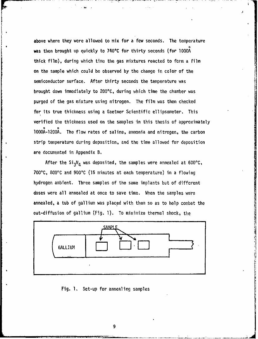
After the Si3N4 was deposited, the samples were annealed at 6000C,
700*C, 800C and 900*C (15 minutes at each temperature) in a flowing
hydrogen ambient. Three samples of the same implants but of different
doses were all annealed at once to save time. When the samples were
annealed, a tub of gallium was placed with them so as to help combat the
out-diffusion of gallium (Fig. 1). To minimize thermal shock, the
Fig.. 1. Set-up for annealing samples
9
Vt
samples to be annealed were placed in the holder outside the quartz
tube furnace, as it was brought up to temperature. The hydrogen gas
was first run through a hydrogen purifier before flowing into the
furnace. The hydrogen flows through the furnace at 226.6 cubic centi-
meters per minute during the warm up period, annealing process and cool
down. After annealing, the samples were pulled from the heating area
but not removed from the furnace, thereby allowing them to cool down to
room temperature. During cool down, hydrogen still flows through the
furnace and over the samples, at the same time being bled off by burning
on i platinum wire. After cooling down, the samples were removed from
the furhace and were ready to be profiled once the cap was removed and
contacts were attached to the samples.
The cap was removed using a 48% reagent hydrofluoric acid (HF), for
usually ten minutes or as long as required. Then the sample was washed
by flowing deionized water over it for one minute (to remove the acid
from the surface) and blown dry using nitrogen gas.
Contacts were then ultrasonically soldered to the four corners of
the sample using pure indium. After soldering, the contacts were
checked with a curve tracer to make sure t ey were ohmic (Fig. 2). If
they were not ohmic, the contacts would be resoldered in an attempt to
correct the problem. If, after resoldering the contacts were still
rectifying they could be sintered by heating the sample to 450'C. This
would reduce the strain in the crystal and the contacts would be more
ohmic in nature as a result of the alloying process.
10
Fig. 2. I-V ,turve for sample contact
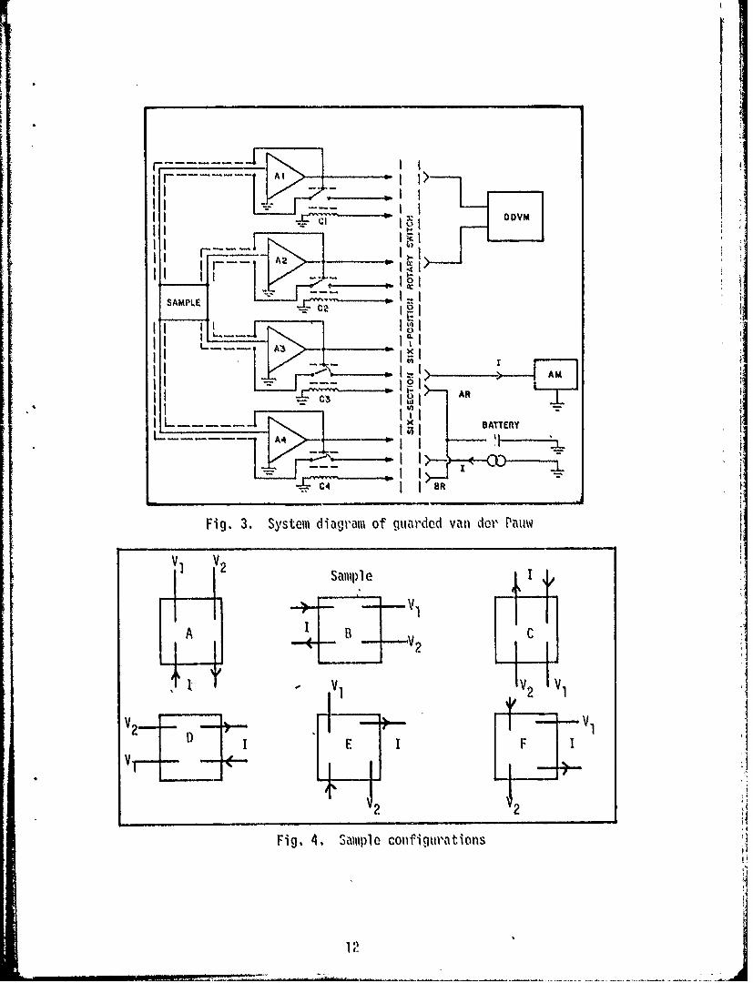
Data Acq~uisition and Processing
The system used for data acquisition was a van der' Pauw measurement
system composed of guarded unity-gain amplifiers (Fig. 3) which provide
144
an input impedance of 10 ohms. This system was used at the Aerospace
Research Laboratory and designed by B, K. Shin. It has a variety of
measurement c,,pabilities such as a guarded Hall and van der Paow
configurations and continuous temperature changes to 4"K using the Air
Product Hel i tran.
The van der Pauw method 'was the only one used in this thesis to
acquire the data, There are advantages in using this method in that
the samples were small and only four contacts were required on the
periphery of an arbitrarily shaped sample. When using the van der Pauw
method, it is required to measure voltage across two leads while current
At 1
II K DDYM
A2A
-. AM :IAM
A4 --------
Fig. 3. System diagram of guardd van dr Paim
V1 '2Samp Ie I
A BV c
V. 1 ~ 2 ~1
E I F
Fig. 4. 'Sam plIe coniUgurations
r
is passed through the opposite leads as shown in Fig. 4 (a-d). Voltage
readings were made by interchanging the leads to the sample. This was
done by a six-position rotary switch which is marked the same as the
configurations in Fig. 4. The last two configurations (e & f) were
used to take Hall voltage readings when a magnetic field is applied
prependicula- to the sample. A total of eight voltage measurements
were made on configurations a-d by reversing the current direction on
each configuration. This way, after averaging all the crystal voltages,
a more realistic value of the samples resistivity would be arrived at.
The Hall voltage was al-so determined more realistically by first applying
the field in one direction and reversing tle current direction, then
reversing the field and reversing the current direction again. There
was then a total of eight Hall voltages from which an average was used
to arrive at a Hall coefficient.
From the average crystal voltage an effective sheet resistivity
was determined using the following equation:
Fs = j A Cv f (al1j) (5)tn2 I c
where s= sheet resistivity
Vc = average crystal voltage
I = applied current
and f = dimensionless correction factor.
The Hall voltage was used to arrive at a Hall coefficient from
the following equation:8AV s 2
S 108 - (cm2/coul) (6)
c
13 -
where Rs = Hall coefficient
AVs = Hall voltage
Ic = applied current
and B = applied magnetic field,
Rs was then used to calculate an effective sheet concentration, Ns , and
mobi I ity, eff:
Ns (qRs)l (cm"2) (7)
where q electron charge
neff ' Rs (cm2 /V-sec) (8)
The above equations are just averages depending upon the distri-
bution in depth of the carrier concentration and the implantation
factors. However, an electrical profile can show what fraction of the
implanted atoms become substitutional, as well as the, spatial location
of the active atoms with respect to LSS theory (see Appendix F). The
electrical profile was obtained by removing thin layers of the sample
at a controlled rate. As each layer was removed, sheet resistivity
and Hall coefficient measurements were taken and the number of carriers
and their mobility was detenviined from the following equations (Ref 1l):
(Rs)i (Rs)$ + 12=en i i2 di (9)
and
1 - 1sli eni'idi (10)
From equation (9) and (10) if follows that
(Rs/ s2 )i
14
and
j ediIti (12)
where di is the thickness of the ith layer removed. The carrier con-
centration, N (cm- 2 ), is obtained from n d.
The degree of electrical compensation is defined as the ratio of
donor to acceptor concentrations, K a Nd/Na * It was not necessary to
compute the values of Nd and Na to find the compensation level. The
only value that had to be determined was the concentration of total
ionized impurities, PI. This was done by using the well known Brooks-
Herring relationship (Ref 11).
3h3 k2 113
16 2e~* P n (1 +f +t1 (3
where vh )2(kr (3 1~
h - Plank's constant
k - dielectric constant
e - electron charge
p - carrier concentration
Pl concentration of total ionized impurities
m* - effective hole mass
To be able to use the above equation, the mobility due to the
ionized impurities (I) must be known, This can be determined from the
following equation:
I 1 + 1 (14)1 A1 V1 L
15
assuming a value of 450 cm 2/V-sec (p-type samples) for lattice mobility
(110,In order to calculate the compensation, K, the following two
equations are used:
P = Nd + Na (15)
p = Nd - Na (16)
These equations can be manipulated to give the following:
PI - p = 2Nd (17)
PI + p = 2Na (18)
from which follows:
PI " P (19)
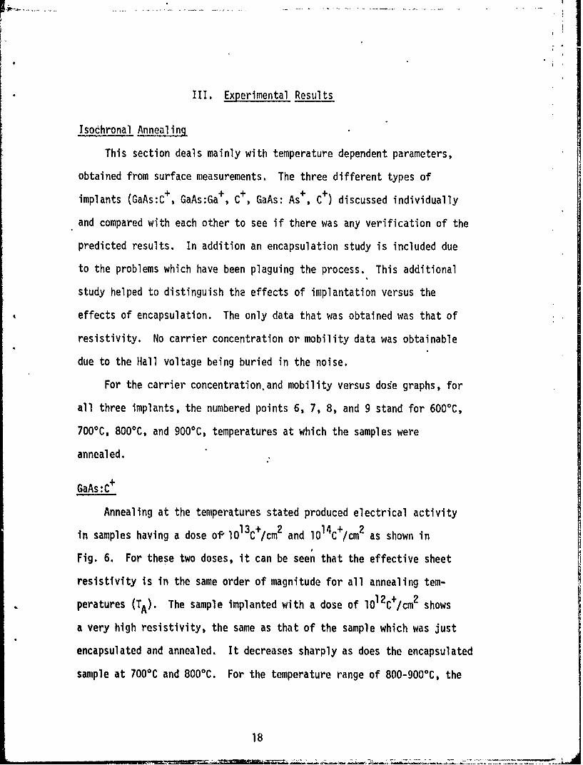
Using equations (13), (14) and (19) a series of curves can be formed by
choosing a vaule for K, such that O<K<I, and a value for p, see Fig. 5.
The removal of these layers was obtained by etching the sample
with a solution of H2S04 : 30% H202: .20 in a ratio of 1:1:50, kept at
OC. The etch removed thin layers of the sample at a predicted rate
of 250 A/min as determined by a Sloan Dektak microtopography on un-
implanted sample. The contacts were protected at the same time to pre-
vent degradation of the ohmic characteristics. This was done by
covering the electrodes with black wax which has been mixed with Itrichlorethylene to a paint-like consistency. After profiling, the
black wax was removed by washing the sample with trichlorethylene, thus
revealing the contacts. Then the sample was taken to the Dektak to
verify whether the etch was still etching at the determined rate. It
was found that the etch actually proceeded at a slower than predicted
16
rate of 144 A/min. After discovering this phenomena each sample was
measured on the Dektak after profiling. The results showed that the
etch rate was the same for the different implants and dosage. Therefore
the implantation of the ions into the substrate must cause some change
in the crystal for it to react in such a manner.
17--------------------------------------------~-.-------A
AIII. Experimental Results
Isochronal Annealing
This section deals mainly with temperature dependent parameters,
obtained from surface measurements. The three different types of
implants (GaAs:C+, GaAs:Ga+, C+ , GaAs: As+, C+) discussed individually
and compared with each other to see if there was any verification of the
predicted results. In addition an encapsulation study is included due
to the problems which have been plaguing the process. This additional
study helped to distinguish the effects of implantation versus the
effects of encapsulation. The only data that was obtained was that of
resistivity. No carrier concentration or mobility data was obtainable
due to the Hall voltage being buried in the noise.
For the carrier concentration, and mobility versus dose graphs, for
all three implants, the numbered points 6, 7, 8, and 9 stand for 6000C,
700*C, 800*C, and 9000C, temperatures at which the samples were
annealed.
GaAs:C+
Annealing at the temperatures stated produced electrical activity
in samples having a dose of 1013c+/cm2 and 1014c+/cm2 as shown in
Fig. 6. For these two doses, it can be seen that the effective sheet
resistivity is in the same order of magnitude for all annealing tem-
peratures (TA). The sample implanted with a dose of lo12C+/cm 2 shows
a very high resistivity, the same as that of the sample which was just
encapsulated and annealed. It decreases sharply as does the encapsulated
sample at 7000C and 800*C. For the temperature range of 800-9000C, the
18
rn/
.111mi, t1r.r
I0
-I A - -C -4
41)
T_ L
f, *I,
/ A.~~0
0 0 1K / 0 /:0 0 0)
rI% \0Ln m
A AI:e
119

GaAs+ +
10~
11
010
5
10i
20 L~
101 ----- _ ---
GaAs.-E 601Kov~c~
113
I-NIEu
112
10
10*200
01)
50
1011 1012 1013 101
Fig. 7. I)npL~ndpIlcL\ o-Fsht hjojl oontailna C'ffCti\'o mobilitY upon C dose (~
resistivity is within the same order of magnitude for the different
dosages and encapsulation. It can be said that there is some observed
implantation effect in the 1013C+/cm2 and 1014C+/cm2 dosages at 6000%
and 700C samples. It is difficult to say this for the 8000C and 9000C
range due to the gathering of all the curves at these temperatures.
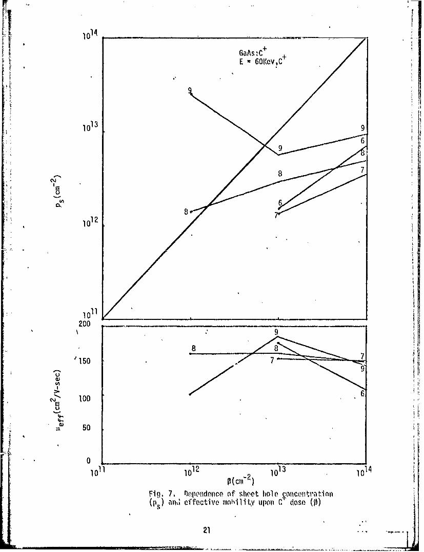
Fig. 7 shows the annealing characteristics of effective sheet
carrier concentration (Ps) and effective Hall mobility (Neff) for
12 + 2different temperatures. For 10 C /1cm , carrier concentration and
mobility were only obtainable for 8000C and 900°%. The carrier con-
centration for 80000 and 9000C increases with temperature but was
higher than the implanted dosage. Also observed was the effect that
the concentration decreased between 6000C and 700%0, and then increased
between 7000C and 9000C for both the 10 3C+/cm2 and 104c+/cm2 samples.
14 + 2Although this trend was observed the concentration for 10 C /cm2 at
113 + 2all annealing temperatures is higher than 10 C /cm samples,
The doping efficiencies (n = P /0) were also determined in this5
study from the diagonal line drawn across the graphs. The results were
compared with previous work done in this area by Sansbury, Harris and
Shin (see Table I). For a dose of 1013c + /cm2, 9000C dnnealed, an
efficiency of 57% was obtained while an efficiency of 9.5% was seen for
a dose of 1014C+/cm 2 annealed at 9000C. These values agree very well
with Shin's findings even though an implantation energy of 60Kev was
* used. The low values obtained in previous studies were probably due to
the low annealing temperatures and encapsulation methods used. In
this study the same annealing temperatures and encapsulation procedures
were used as by Shin (Ref 4),
22
u L. st. S-'* 0 0 0 0i n IA3 3
C 0 CA V) S- S
4.- to Vn V) (n. to F- U t-- F- U)
N N C4 N~ Z:~Z0) C. 0 0 0 0) 0 m~ m) m) m~ m m
>0
4-4- C. a)e Le 0 0 0 utO 0 C)
E w %.- C- N N r -0 r" a- (aU rE U o Y
.I- a
S.4-)
S. - I
to 06 0:1 0a) 0 0 0= %- 0h 0~ 0l 0 0 0 0t 0 0 %0D
L) 0l 0c 0O -c 0 0 0- 0~ 0 0 + +go 0. 0 N N (0
U000
r- to
0 C) C) C) 0 C) CD C)0 aC
N- a- r.- 00 00 M- a- CN a- 0 a
a 0 ) 0 0 0 0 0 0
U -a -XXa-a -a -aCN N)C
23

- -4
From the Hall mobility we can also see the effect that a dose of
lO13C+/cm2 annealed at 900C is more effective than a dose of 1O14C+/cm2
The mobility is higher for lO13C+/cm2 dose than l014C+/cm 2 dose for all
temperatures but lower than obtained in previous studies. This higher
mobility could result from the encapsulation problem.
GaAs:Ga+C+
The effective sheet resistivity (fs) for GaAs: Ga,C at the
different annealing temperatures (Fig. 8) looks very much like what
was observed for GaAs:C + . The encapsulation and lol2Ga+ C+/cm 2 samples
were high, while lol3Ga+, C+/cm 2 and lol4Ga+, C+/cm 2 dose samples were
in the l04 and lO5 ohms per square (n/13) range. Another observation
made was that all the dosages in the 8000C to 9000C range had lower
resistivities than the GaAs:C + samples in the same range.
More observations can be made by looking at Fig. 9 which shows
the effective sheet hole concentration and effective Hall mobility as a
function of implanted dose (0). First, it is evident that for every
temperature the hole concentration is greater for 1014Ga+, C+/cm2 than
l03Ga+, C+/cm2. The most promising fact is that at 900%0 for 104Ga+,
C+/cm 2 the hole concentration is 3.23 x 10¹³/cm3 which is an efficiency
of 32%, a noticable improvement over just carbon implants. However for
the l013Ga+, C+/cm 2 dose at 80000 we have an efficiency of 87%, which
is also a large increase over the same dose and temperature for Just
carbon implants.
The effective Hall mobility also showed a trend, in that at the
lol 4Ga+, C+/cm2 dose the carbon implants alone were much higher than
24- r " r ':K ':C = Z , . . . ... . . , . .... . . . . . . . . . . . .
1010GaAs: Ga + C+E 12Q1" ' G
10 12 6QKev, C
10
108 * CAPPINiG
10
1010
0bO 700 80090T A( C)
Fig. 8. Evvective sheet rosistpvitq(ivs. annealinig temp. (T A) for Ga ,C
- 25
1 0 1 4 a s G + + +
E 120ev, G1013v,
-S9
N8
26
10 126
1011200
-150
cU 100
04- s0
0 101 101 10 1
Fig 9.Deplidnceof shoot hole cp1ceoltration) and effective mobility Uponi Ga ,C dlose (0)
26
the Ga+ , C+ implants. In addition, there was an observed decrease in
13 1mobility from 10 to 1l4 doses in both cases for all temperatures
except at 7000C.
GaAs:As+, C+
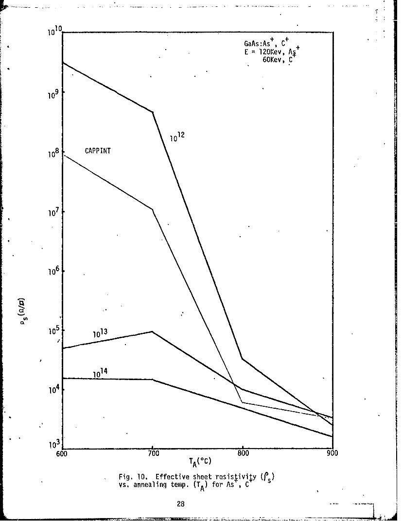
The effect sheet resistivity Fig. 10 shows the same trend as that
of the C+ and Ga+, C+ implants. Only a small difference can be seen in
the I014 dose where the sample has a little higher resistivity in the
600*C to 7000C temperature range. The graph also shows the same trend
as the others, that is, from 8000C to 9000C they all come together.
This makes it very hard to determine if this effect resulted from en-
capsulation or implantation effect.
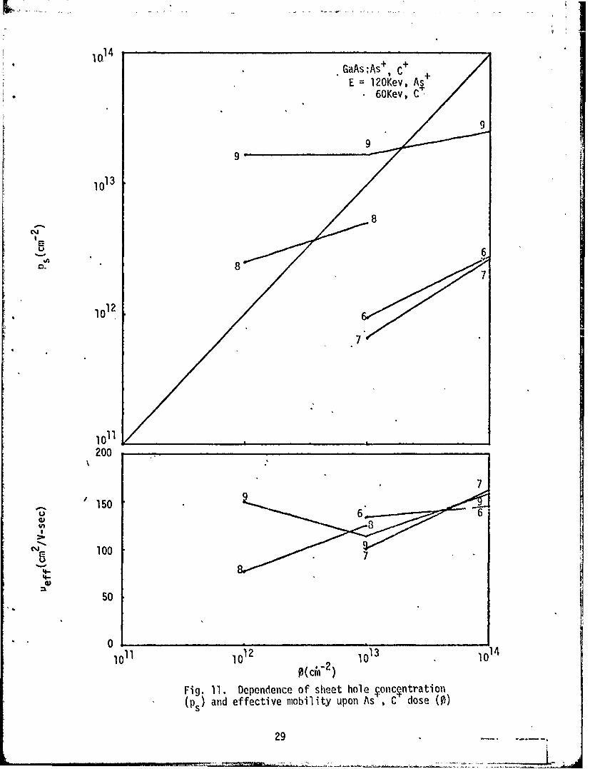
Looking at Fig. 11 we still observe the strange phenomena of the
concentration being larger than the implanted dose this time for a
1o3As+, C+/cm2 dose at 9000C annealed. This characteristic may also
have been observed for Ga + , C+ implants if it were possible to measure
the Hall voltage. Also observed was that for 600C and 7000C annealing
temperatures at 101 3As+, C+/cm 2 and l014As+, C+/cm 2 dosages the con-
centration was lower than for all the other implanted samples. Also,
the efficiency for the sample annealed at 9000C at a dose of
1o14As+ , C+/cm2 was 25%, which is lower than the Ga+ , C+ implants but
much higher than the C+ implant.
The effective Hall mobility plot shows that at 1014 dose for all
+temperatures the mobility is in the same region as for C implants but
higher than for the Ga+ , C+ implants. At the same time, the 1013 dose
of As+ , C implants for all temperatures had mobilities which were
lower than the C+ implants and in the same region as the Ga+, C+ implants.
27
10 10
>GaAs:As, C+E l2O1'ev, A
L
6Kev, C
10 12
10 8 CAPPINT
107
10
101
600 700 80090TA ( C)
Fig. 10. Effective sheet resistivip~ (FS)vs. annealing temp. (TA) for As ,C
-- ~~28 .. j i
1014*1GaAs-A+ C +~
E 1 2OKev, A6OKev, C
1013
10 1
CI 100
150
* 50
Fig. 11. Dependence of sheet hole .oncpntration- (p5) and effective mobility upon As ,C dose()
29
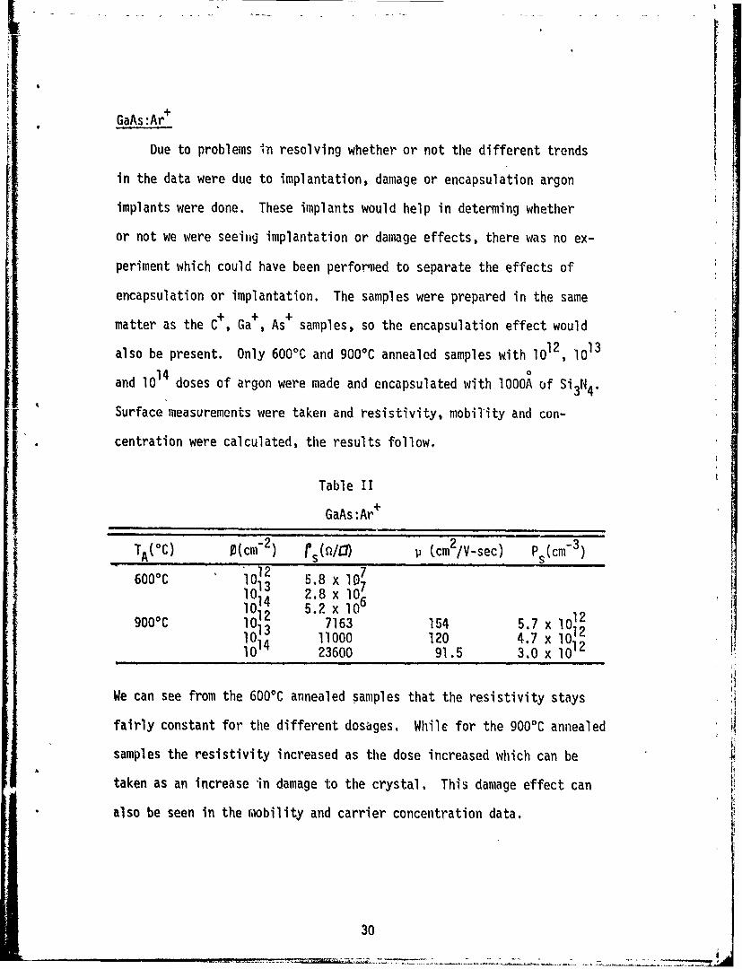
GaAs :Ar+
Due to problems In resolving whether or not the different trends
in the data were due to implantation, damage or encapsulation argon
implants were done. These implants would help in determing whether
or not we were seeing implantation or damage effects, there was no ex-
periment which could have been performed to separate the effects of
encapsulation or implantation. The samples were prepared in the same
matter as the C+ , Ga+, As+ samples, so the encapsulation effect would
also be present. Only 600 0C and 9000 C annealed samples with 1012, 1013
and 1014 doses of argon were made and encapsulated with IOOOA of Si3N4.Surface measurements were taken and resistivity, mobility and con-
centration were calculated, the results follow.
Table II
GaAs :Ar+
TA(0C 0(cm-2 rs(0/0) (cm2/V-sec) P s(cm 3 )
6000 C 1012 5.8 x 10⁷
1013 2.8 x 100 5.2 x 1069000C 1013 7163 154 5.7 x 10121013 11000 120 4.7 x lO1 2
1014 23600 91.5 3.0 x 10¹²
We can see from the 600C annealed samples that the resistivity stays
fairly constant for the different dosages. While for the 900C annealed
samples the resistivity increased as the dose increased which can be
taken as an increase 'in damage to the crystal. This damage effect can
also be seen in the miobility and carrier concentration data.
30
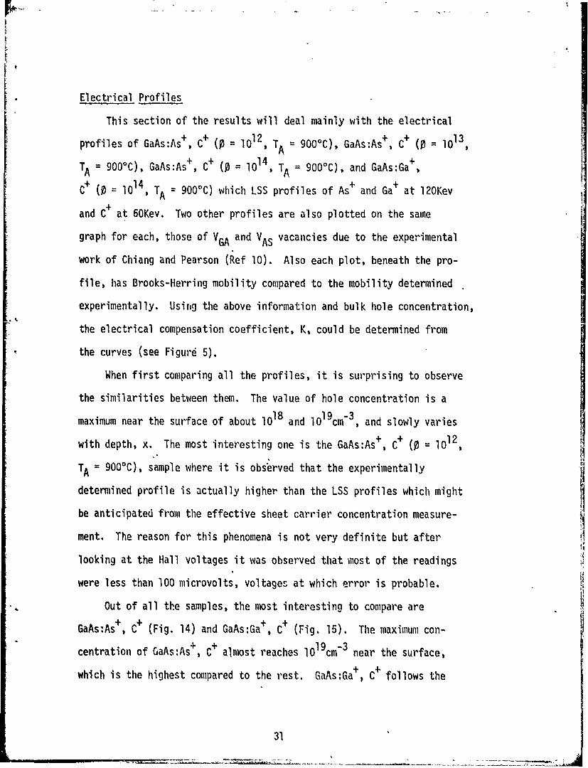
Electrical Profiles
This section of the results will deal mainly with the electrical
profiles of GaAs:As+ , C" ( = 1012, TA = 900C), GaAs:As+ , C+ (0 = 1l13
TA 9000C), GaAs:As , C+ (B = lO14 , TA = 900'C), and GaAs:Ga
C ( =10 14, TA = 900'C) which LSS profiles of As+ and Ga+ at 120Kev
and C+ at 60Kev. Two other profiles are also plotted on the same
graph for each, those of V and VAS vacancies due to the experimental
work of Chiang and Pearson (Ref 10). Also each plot, beneath the pro-
file, has Brooks-Herring mobility compared to the mobility determined
experimentally. Using the above information and bulk hole concentration,
the electrical compensation coefficient, K, could be determined from
the curves (see Figure 5).
When first comparing all the profiles, it is surprising to observe
the similarities between them. The value of hole concentration is a
maximum near the surface of about 1018 and 10 19cm 3 , and slowly varies
with depth, x. The most interesting one is the GaAs:As+, C+ ( = 1012
TA = 900C), sample where it is obs'erved that the experimentally
determined profile is actually higher than the LSS profiles which might
be anticipated from the effective sheet carrier concentration measure-ment. The reason for this phenomena is not very definite but after
looking at the Hall voltages it was observed that most of the readings
were less than 100 microvolts, voltages at which error is probable.
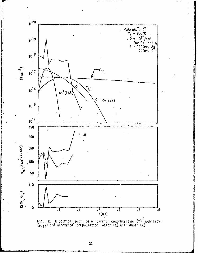
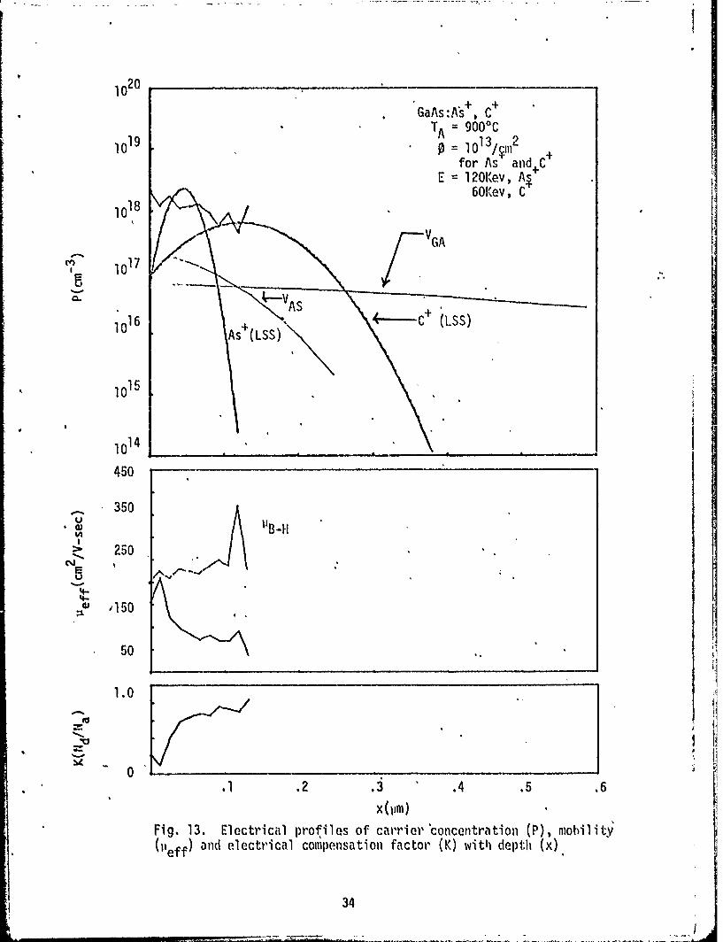
Out of all the samples, the most interesting to compare are
GaAs'As + , C+ (Fig. 14) and GaAs:Ga+, C+ (Fig. 15). The maximum con-
centration of GaAs:As+, C+ almost reaches 1o19cm'3 near the surface,
which is the highest compared to the rest. GaAs:Ga+t C + follows the
31-- --.- r - -. - ~ ---- ,. ..
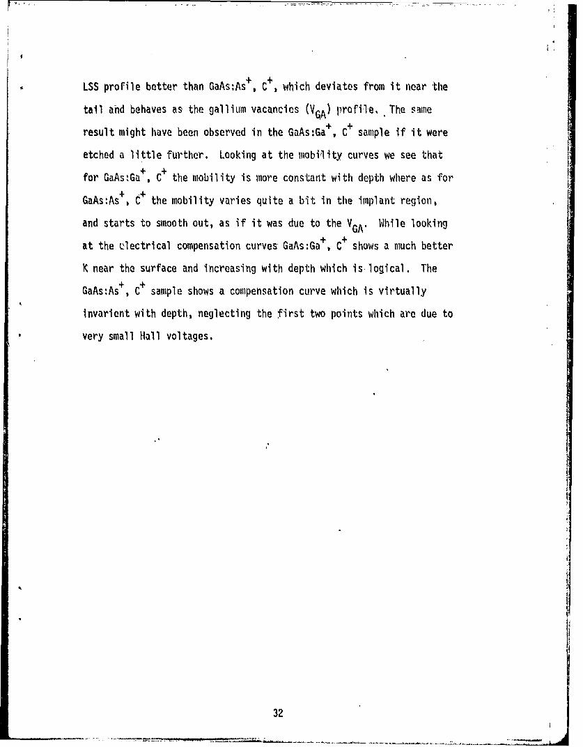
LSS profile better than GaAs:As+, C+, which deviates from it near the
tail and behaves as the gallium vacancies (VGA) profile, ' The sime
result might have been observed in the GaAs:Ga+ , C+ sample if it were
etched a little further. Looking at the mobility curves we see that
for GaAs.Ga+, C+ the mobility is more constant with depth where as for
GaAs:As + C+ the mobility varies quite a bit in the implant region,
and starts to smooth out, as if it was due to the VGA. While looking
at the electrical compensation curves GaAs:Ga+ , C+ shows a much better
K near the surface and increasing with depth which is, logical. The
GaAs:As+, C+ sample shows a compensation curve which is virtually
invarient with depth, neglecting the first two points which are due to
very small Hall voltages.
3
32
*GaAs:As, -C +TA 900%0
10 for As andE 12OKev, A
1018 6Ov, C
11;
101
10175G
114
450
350
U 250
~ 501
.0
~ 0
.1 2 .3 .4 .-
Fig9. 12. Electrical profiles of c(Irrlier colncontxationl (11) mobi Ii ty,~"f~and eleoctri cal componsati on Faictor (K) With deptil (X)
33I
120GaAs:As+ c +
TA = 9000C10 19 0 = 1013 4.1112 +
for As and. C~E = 201 ev, A
60*,v 01
1015
i17
30
250.
25
W 150
50
1.0
* 1.2 .A .4 .5 .6
Fig. 13. El ectri cal prof ile s of carrieor 'concentra tion (P) , mobiIi tyN"eff) and electrical coimpensation factor (K) with depth (x).
34
1 2OGaAs:As, 1 + 2~10 /cm
10l19 T A 9000C
10 18
1016
1015'
1014450
350
-
0
.1.2 .3' .4 .5 .
Fig. 14. Electrical prof ilIes of carrier concentration (1)), molility
35
1020 + *F-GaAs:Ga ,.
T TA = 90011C10 19 = 1014 cm 2 f~or
Ga+ and CE 1 l20Kev, G.~
18 6OKev, C
101
1015A
45
4 50
~. 250
4- .150
50 '
1.0
*0
0 1.2 .3 .4 .5 .6x(pill)
Fig. 15. El ectri cal prof ilIes of carrieor 'concentratfon (P), mlobi1i ty6'fand electrical compensation factor (K) 'withi depth (x)
36
IV. Discussion of Experimental Results
From the data acquired on isochronal annealing two features can be
seen inediately. For all the different types of implants, at annealing
temperatures of 6000C and 7000C, the resistivities for the 1012 samples
are very high, higher than just encapsulated samples (no implants).
As data from GaAs:Ar+ implants indicated that the resistivity is high.
However, 1013 and 1014 dose samples for all implants show low resistivity.
Such a difference in resistivity with dosage suggest there is a strong
dose dependence with annealing temperature. In fact,, it is so dose
dependent that no matter what the implants may be, this effect was
observed. At the higher annealing temperatures the resistivities are
all the same order of magnitude, suggesting that the thermal effect pre-
dominates the resistivity. At these temperatures the encapsulation
(with which there has been some problem) could act as a sink, drawing
out the Ga and As, and causing vacancies to be formed. This possibility
may also account for the observations made with the 1012 dose samples,
annealed at 800% and 900% which s6ow a doping efficiency of greater
than 100%. The Hall voltages measured on these samples were less than
100 microvolts and very unstable which is subject to error. The crystal
voltage (which was higher and more in the range of accuracy of the
equipment) also displayed a strange phenomena. Crystal voltages from
one configuration to the next changed drastically, sometimes by a factor
of six, indicating there was severe inhomogeneity, as can be seen in
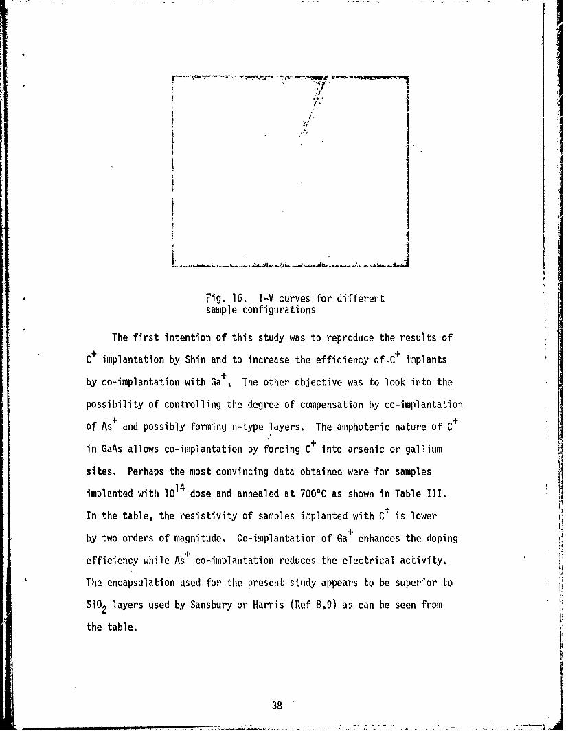
Fig. 16 by checking for ohmic contacts in different configurations.
37
'
IIii
IIII
II
Fig. 16. I-V curves for differentsample configurations
The first intention of this study was to reproduce the results of
C+ implantation by Shin and to increase the efficiency of C + implants
by co-implantation with Ga+ The other objective was to look into the
possibility of controlling the degree of compensation by co-implantation
of As+ and possibly forming n-type layers. The amphoteric nature of C
in GaAs allows co-implantation by forcing C+ into arsenic or gallium
sites. Perhaps the most convincing data obtained were for samples
implanted with 1014 dose and annealed at 7000C as shown in Table III.
In the table, the resistivity of samples implanted with C+ is lower
by two orders of magnitude. Co-implantation of Ga+ enhances the doping
efficiency while As+ co-implantation reduces the electrical activity.
The encapsulation used for ' the present study appears to be superior to
SiO 2 layers used by Sansbury or Harris (Ref 8,9) as can be seen from
the table.
38

Table III
Electrical Characteristics of l14
dose and 7000C annealed samples
11 2 2
Sample s Old) eff(C P/V-sec) p (.cm )
Encapsulation 1.08 x 10⁷
GaAs:Ar+ 5.01 x 1O6
GaAs:C + 1.17 x 10⁴ 150 3.57 x 1l2
GaAs:Ga +, C+ 4.56 x 1O3 114 1.20 x 1l3
GaAs:As +, C+ 1.47 x l04 162 2.63 x 10¹²
Sansbury 2.72 x lO4 242 9.50 x l0 ol
In addition, other supporting results are shown in the 10 4/cm2
9000C annealed, GaAs:Ga + , C+ , GaAs:As + , C+, and GaAs:C+ samples.
Efficiency is highest for the Ga+ co-implantation with a value of 32%.
As+ gave an efficiency of 25% while C+ alone was only 9.5%. Although
the As + C+ co-implantation was expected to be lower than the C+ alone,
the gross damage effect due to the heavy ions seems to aid the effici-
ency obtained in these samples at this annealing temperature. The
annealing behavior discussed so far can. be more clearly observed from
the profiles obtained. The GaAs:As+ , C+ sample of 1012/cm2 dose,
annealed at 900%0 (Fig. 12) is most peculiar of them ail, since the
concentration profile is substantially higher than either LSS profile
or sublattice vacancy profile obtained from Pearson and Chiang (Ref 10).
This phenomena suggest, as stated previously, the encapsulation may act
as a sink and enhance the out-diffusion of the sublattice atoms. It
would account for the high p-type concentration at the surface. This h
observation is reinforced by comparing the concentration profile to the
39
gallium vacancy profile, which changes as a complementary error function.
The concentration profiles appear to be independent of dose or type of
implants as can be seen by comparing Fig. 12 through 15. This indicates
that it is very difficult to separate the effects due to encapsulation
from those due to implantation using the profiles. In spite of this
difficulty, it is still interesting to compare the 1014/cm2, 9000C
samples of GaAs:As+, C+ and GaAs:Ga+, C+. It can be observed from
Fig. 14 and 15 that Ga+ co-implantation gives better'profile integrity.
This can be seen from the low compensation coefficient near the Ga+
implanted area. On the other hand the As+ co-implantation gives a broad
profile with no sharp average change in compensation with depth. The
high bulk concentration (10l/cm3) near the surface in Fig. 14 might be
due to damage enhanced doping effect as indicated by the high compensation
value in this region.
I
40 l

V. 'Sumary, Conclusion and Recomlendations
This thesis looked at the possibility of co-implantation of As+
and Ga+ with C+, in order to reduce the electrical activity of the
dopant in one case, and to increase in the other. GaAs was doped with
C+ alone and with equal doses of As+ and Ga+ to maintain the stoichi-
ometry of the crystal. The samples were all encapsulated with the same
material and thickness, and annealed for the same period of time. The
samples implanted with C+ only were done to verify Shin's results and
used as a reference for the co-implantation samples. Only surface
measurements were made on most of the samples due to the extended amount
of time required to profile each one. The only ones that were profiled
were the 9000C annealed samples. Only five profiles are presented
because it was not possible to obtain any Hall voltages on the others in
addition, the etch rate was so fast that after two etches the implanted
region was passed. The samples for which no profiles were obtained could
have been run aga-n but the ion implantation facility was not operational,
and therefore could not produce mor samples. From the data obtained, it
is seen that some of the predicted results were verified.
The results presented in this thesis have shown to some extent that
the addition of Ga+ or As+ implants to the primary implants C+ , has an
effect on the doping efficiency and crystal lattice. This effect is
due to the encapsulation, which may be acting as a sink for out-diffusion
++of gallium vacancies, the enhancement of site location due to the Ga+ ,
As+ implants, and possibly the damage of the sublattice. All these
effects contribute to the efficiency which was observed, but they must
be studied separately to see how much each one contributes.
41
Additional work should be carried out in co-implantation for con-
trolling the stoichiometry of the GaAs, which shows some promise for ion
implantated layers. More measurements should be acquired to show the
reproducibility of this process. The encapsulation which has plagued
this work should be more thoroughly researched as it hinders the
observation of implantation results. The damages and reactions produced
by the implantation of Ga+ and As+ should also be looked into. Temper-
ature dependence measurements should be made to better distinguish the
effects which are dominant in the conduction process. Different
annealing schemes should also be tried. For example, annealing could
be dcne after Ga+ or As+ implantation, followed by implantation of the
primary species with post annealing. This may relieve some of the
damage due to the heavy ion implantation.
42
Bibliography
1. Heckingbottom, R. and T. Ambridge. "Ion-lmplantation in CompoundSemiconductor-An Approach Based on Solid State Theory." RadiationEffects, 17:31-36 (1973).
2. Hilsum, C. Semiconductinq III-V Compounds. New York: PergamonPress, 1961.
3. Lyons Jr., R. P. Ion Implantation of Diatomic Sulfur into GaAs.Unpublished thesis. W-ight-Patterson Air Force Base, Ohio: AirForce Institute of Technology, September i974.
4. Shin, B. K. "Carbon Ion Implanted Gallium Arsenide." AppliedPhysics Letter, 29:438-440 (October 1976).
5. Stolte, C. A. "Dual Species Ion Implantation into GaAs." To bepublished.
6. Woodcock, J. M. "Enhancement of the Donor Activity of ImplantedSelenium in GaAs by Gallium Implantation." Applied Physics Letter,28:226-227 (February 1976).
7. Rodine, E. T., R. R. Berliner and B. K. Shin. Ion Implantation inCopound Semiconductors. AFAL-TR-76-218. Wrig-ht-Patterson AirBase, Ohio: Air Force Avionics Laboratory, January 1977.
8. Sansbury, J. D. Technical Report no. 4725-2 (prepared under ARPACenter for Materials Research Contract C-0218 and National ScienceFoundation Grant GK 4290), Stanford U., Stanford, Calif., 1970(unpubl ished).
9. Harris, J. S. International C61ference on Ion Implantation inSemiconductors. Edited by I. Ruge and J. GrT-l -(springer-Ver-ay,Berline, 1971, pg. 1571).
10. Chiang, S. Y. and G. L. Pearson. "Properties of Vacancy Defects inGaAs Single Crystals." Journal of Applied Physics, 46:2986-2991(July 1975).
11. Johansson, N. G. E. and J. W. Mayor. "Technique Used in Hall EffectAnalysis of Ion Implanted Si and Ge." Solid State Electronics,13:317-335 (1970).
12. Gibbons, J. F., W. S. Johnson and S. W. Mylroio. Pro'jected Rang
Statistics Semiconductors and Related Materials. Pennsyl vaia:Halsted Press.
13. Johnson, W. S. and J. F, Gibbons. Projected Range Statistics inSemiconductors. Stanford U. Bookstore.
14. Sze, S. M. Physics of Semiconductor Devices. New York: Wiley-Interscience, 1969.
43
Appendix A
Definition of Symbols
F(g) a foreign atom in the gas phase
FGA, FAS a foreign atom on a Ga or As lattice site in GaAs
Fsi a foreign atom on a Si lattice site
h a hole in the valence band
e an electron in the conduction band
x, 'and' supperscripts denote neutral, single positively chargedand single negative charged species respectively
VAS' VGA a vacant site in the arsenic or gallium sublattice
Gai, Asi a gallium or arsenic atom on an interstitial site
(Ref 1)
44
44
2 .... -...." ..I '

0 w
.~. 0 0 0 0 0 0 0 0 0
L) IJu I I U u
00) () 0) 4;0) t) 0)0)
1- C~) Cl Cl C4) CV) CV) C
co 00 00 0co00 c
>1 * Ch cn0) A r% 0% moo~
U" ZC.. LAU ) LC) LO LO LA l)LO-.o - % l 0 ~ ~ ~
, C) CD~ 0 00 000)CD(Dar- ~ L) C'CO C\ CC'C' U) O n L U LOLC
Co'4J
0
C) N.) 00 00 0CDa0 0mL u A C) CD C) a A LA C) LA LA
4.-
" ) 00CDC)0 000 000)C)Cs- l. CD Co C> ao CD CD Co Cl C
u- (n' m ' CL' U) C) CL Ln LO L
U-U
++
45
Appendix C
SiO, "l'h10.1,vis R~atre sljNA "llmv Range
Otdcr Color (11nt) (pll)
Silicon 0-0.027 0,0,020lrown 0.077-0.053 0.020-0,0 0Goelln l1rowil 0,053 A0073 0,040.SRed 0,073,0,097 0,0 5 .010'13Deep le 0.097-0,010 0,073 0,077
1s1 13htc 0.10-0.12 0.077/- 0.0)31,11 111w. -,, 0.093-0.0
Vcry Pl ltleiu 0.13.0.15 0.1 0, ISilicon 0.154016 O, I1 0.12.Light Yellow O,.16-0.1I7 O, I 2,0, 3
Yellow 0. 1 7-0.0.0 13- 0, 15Or nge R d 0.20-0.,N 0.11 0.13
st 0,d-0S Illk Red 0.02 S 0.19 0.21
21ld 111w V.0.,031 0.21,103
Iloe.(ral 0.31-0,33 0.23, OXUViL,ht Gwen 03- T02SO2Olalt',c Vdllow 0.37-0.10 0.2,%0.302nd 0 d 0.,0-0,4 0.30 0,33
AISINX.) 1.97 SiO, tli,:l.wm'T r lo o1f I'm v1 ilk\ .......... , 1.33 a-4(sqlO ) I..1%,i N4 thivklmm' I
Fig. C.l Color corresponding to varyinqthicknesses of the deposited layer
i
46
Appendix D
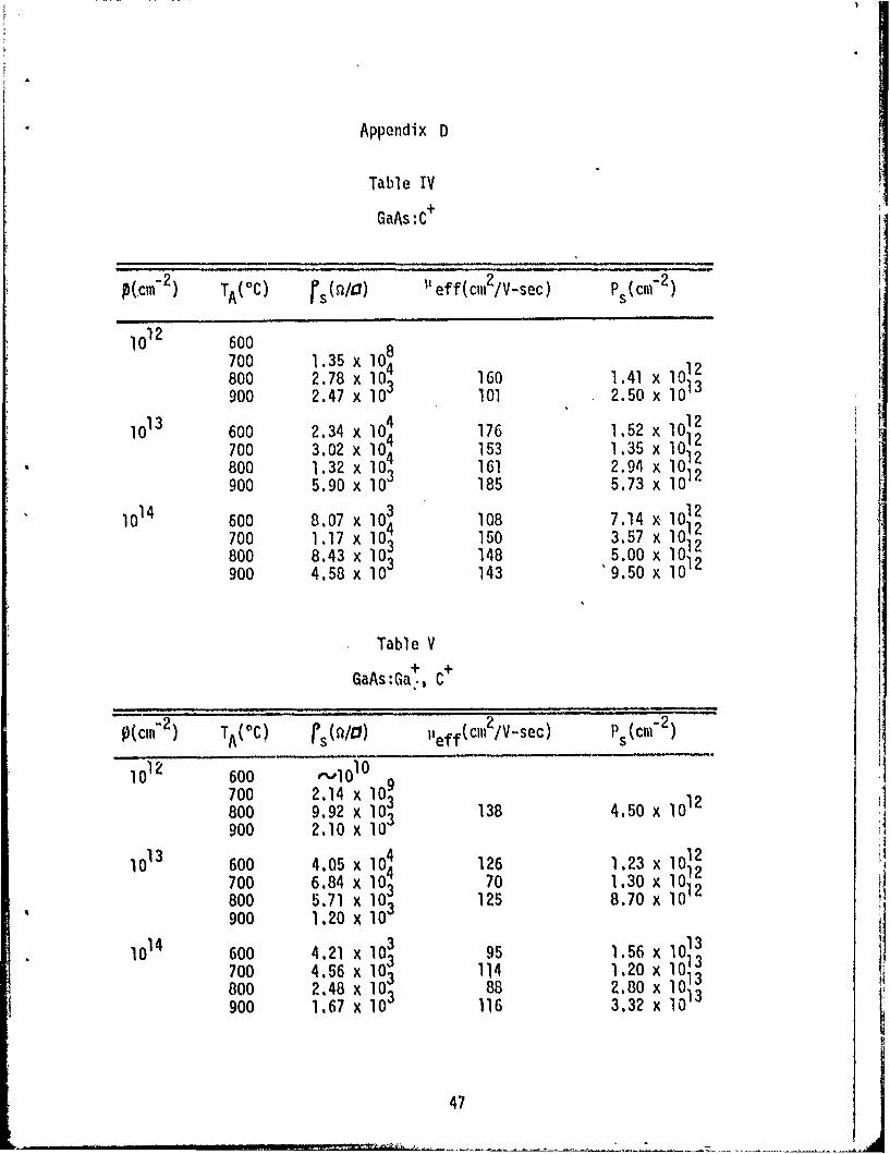
Table IV
GaAs: +
P(cm2 ) TA(OC) 1s(n/) 1eff(cm /V-sec) Ps(cm-2)
102 600
800 2.78 x 10⁴ 160 1.41 x iO10900 2.47 x l 101 2.50 x 10¹³
0600 2.34 x 176 1.52 x 1O12700 3.02 x 10⁴ 153 1.35 x 1012800 1.32 x 10⁴ 161 2.94 x Io12
900 5.90 x 10 185 5.73 x lO12
10600 8.07 x 1A108 7.14 x102700 1.17 x 10' 150 3.57 x O1 2
800 8.43 x 10³ 148 5.00 x 1012900 4.58 x 1 143 *9.50 x 1012
Table V+ +
GaAs:Ga+, C
O(cm 2) TA(DC ) FS (1/1/) leff(C" 2 /V-sec) Ps(cm 2)Ls
lO12 600 1 O
700 2.14 x 10903 13 .0Xl 1 2
800 9.92 X 10³ 138 4.50 x 1
900 2.10 x W
1l3 600 4:05 x 10 126 1.23 x 170 1.30 il2700 6.84 x 10⁴ 705 1.30 x 10¹²
800 5.71 x 10³ 125 8.70 x 1012900 1.20 x 10³
1l4 600 4:21 xl0 95 1.56 X 101341561 01 114 1.20 x113
800 2.48 x 10³ 88 280 x 1013
900 1.67 x 10 116 3.32 x 10¹³
47

Table VI
GaAs;As+, C+
Sm2) T(s (/D) eff(cmn2/V-sec) Ps (cn 2 )
1012 600 3:10 x 109
800 3.26 x 10⁴ 77 2.50 x l 12
900 2.50 x l03 150 1.66 x lO1 3
l 1 3 600 4.95 x 10⁴ 134 943 x lOl
700 9.41 x 10 4101 6.58 x 1011800 9.97 x 10³ 125 5.00 x I012
900 3.31 x 10 114 1.66 x 10¹³
1014 600 1.55 x 10⁴ 145 2.77 x 1O1 2
700 1.47 x 14 162 2.63 x 1012800 31
900 1.59 x 10³ 158 2.50 x 10¹³
Table VII
Encapsulation
TA(. 0C) s(/7D)
600 9.22 x 10⁷
700 1.08 x 10 7
800 6,02 x 103900 3.20 x l0
48
5
nmas' (B. 2)
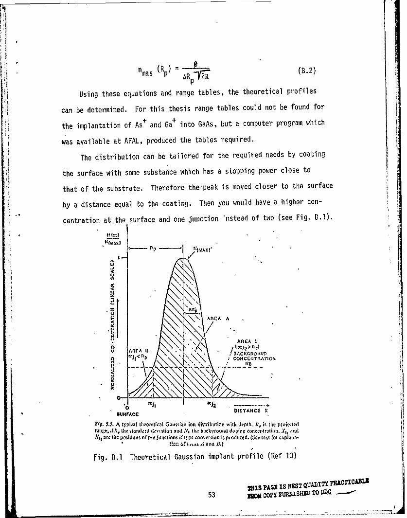
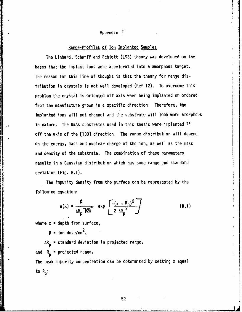
p
Using these equations and range tables, the theoretical profiles
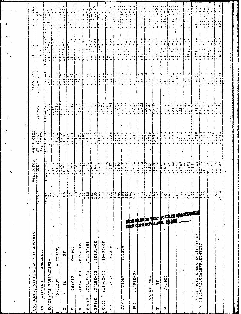
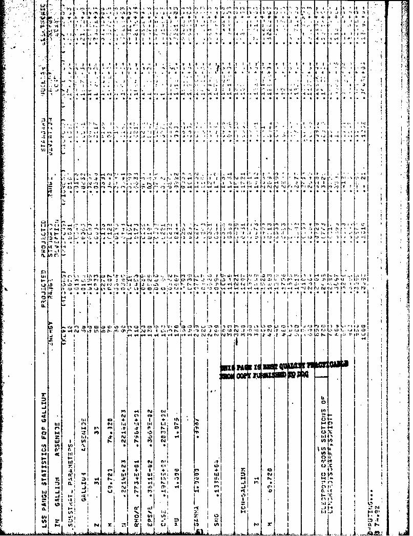
can be determined. For this thesis range tables could not be found for
the implantation of As+ and Ga+ into GaAs, but a computer program which
was available at AFAL, produced the tables required.
The distribution can be tailored for the required needs by coating
the surface with some substance which has a stopping power close to
that of the substrate. Therefore the-peak is moved closer to the surface
by a distance equal to the coating. Then you would have a higher con-
centration at the surface and one junction Instead of two (see Fig. 13.1).
film)
LI
AIACA A
" "' / n'
0 ArA n.S % 14 rF tP IACKGR Olt; 1
"1/4 ':',,, 6$,,.z -n __,)_SURFACE OIlTANCU :
rig i.i. A typic~it thworctkio Gatiln~u iont distribution wid, depth. R, ik tile proi~'ctt
XisatC tile Poitions Orp-.O junctions V~tyrc coumersion is produiced. (Scc tc.\t (er c~.pbla.
Fig. B.1 Theoretical Gaussian implant profile (Ref 13)
=IS PAGE IS BEST QUALITI: F'TICl
53 -" Cwl JuRNISHED TO D,.Q . -
----- - -- - ---
T I tT, l4 ° ),* • ,
1 '4 .- 4 1 1....
" . i n
44 4 4 *4 *.f a a * •
11 A
,. * g * a a * * 4 4 9 4 4 a 4 9 * *
-4 ".1 4 .14.1- 44 ' ' '
f
I
A 1 4I j
.. ..1 . .
s SI#. 1. 11 1a 4 1* N * (V . 1. 'A n
. ij--
k. 4 I el -.4 -41,4 1
4 4 1-) r VA 1 j N 1) 1 ' .4 IN) V)t1. m tt")UNt JL V
1 1- \A C' 2 i'l W1 " ) 0
ILI #
+ I + I + C)Itit I ti la oi I -
i~.ifw t. Iq I
IA o VII ). 0 0 L 0,
(3 1. n 4 Ia
4-4 1N 4l 9-Ii ~% fe :. "M " "
'.0 1 -Al iF
1 "0 1 + "1 4 + 0, :l 1 S"
'V'IS IS .S SO IS ..I 41 * , IS
'"*~ " .... "
* * . .I.. . .. I. • "" 00'' ". . ......... 0
S,
I .
. .~ S. *. . .~ . .74 . IS 0 0 . .0 0
I CIS IN I 1,
illi.. a .. .. .1 . . . S O
* I ,{
- t I1 1 It "I* V * -1
-J. I,, I ,N . -e N. N I,
I I S IS1 ,
4t ji I-L z . j j I=Li 11. 1L KL ~ SL:~ID 11 on. 14I4 4.1 11 Iq %. -
- iAppendix F
Range-Profiles of Ion Implanted Samples
The Linhard, Scharff and Schiott (LSS) theory was developed on the
bases that the implant ions were accelerated into a amorphous target.
The reason for this line of thought is that the theory for range dis-
tribution in crystals is not well developed (Ref 12). To overcome this
problem the crystal is oriented off axis when being implanted or ordered
from the manufacture grown in a specific direction. Therefore, the
implanted ions will not channel and the substrate will look more amorphous
in nature. The GaAs substrates used in this thesis were implanted 70
off the axis of the [100] direction. The range distribution will depend
on the energy, mass and nuclear charge of the ion, as well as the mass
and density of the substrate. The combination of these parameters
results in a Gaussian distribution which has some range and standard
deviation (Fig. B.l).
The impurity density from the surface can be represented by the
following equation:
0 -(x - RD) 2n(W) = _p _ . exp 2 '.1)
AR P2 Lz E2AR pwhere x - depth from surface,
- ion dose/cm,
ARp standard deviation in projected range,
and Rp projected range.
The peak impurity concentration can be determined by setting x equal
to Rp
52
nmas (R)= - (B.2)P' AR p 2Ii
p
Using these equations and range tables, the theoretical profiles
can be determined. For this thesis range tables could not be found for
the implantation of As+ and Ga+ into GaAs, but a computer program which
was available at AFAL, produced the tables required.
The distribution can be tailored for the required needs by coating
the surface with some substance which has a stopping power close to
that of the substrate. Therefore the-peak is moved closer to the surface
by a distance equal to the coating. Then you would have a higher con-
centration at the surface and one junction 'nstead of two (see Fig. B.1).
AAC
' " AREA b 0
AREA >{CONCWTRAVIOtt
o__0
4'
0
SURFACEV C x
rig. M... A typical Wh~rclic,-11 Gatialn in distributtionl with depth. R, i,. fl proi,. Vtck
'atllce, 4|14, the standerdt tio'ttion and ,V, the backgrouid dophnR c:otcotr tio n. , anr d
azre the positions ofp.n jonctions ityr,: c mn erson is produced. (,1cc wC\c fLr c.pJi-.*t.- - , allu A.)
Fig. B.1 Theoretical Gaussian implant profile (Ref 13)
281S pAGI IS BBST QUALITT f CflCIIM
5M Ofl JUMISHID TO D-
VITA
Michael Stefiniw was born August 23, 1954 in Passaic, New Jersey.
He graduated from Morris Catholic High School in 1972 and attended
Stevens Institute of Technology in Hoboken, New Jersey. He received
his commission from ROTC in May 1976. His first assignment was the
Air Force Institute of Technology, Wright Patterson Air Force Base,
Ohio, where he is enrolled in, the Graduate Electro-Optics program.
Permanent Address; Smithtown RoadHackettstown,New Jersey 07840
54
UnclassifiedSECURITY CLASSIFICATION OF THIS PAGE (When Dates fintered)
C REPORT DOCUMENTATION PAGE ___I__N___TORM
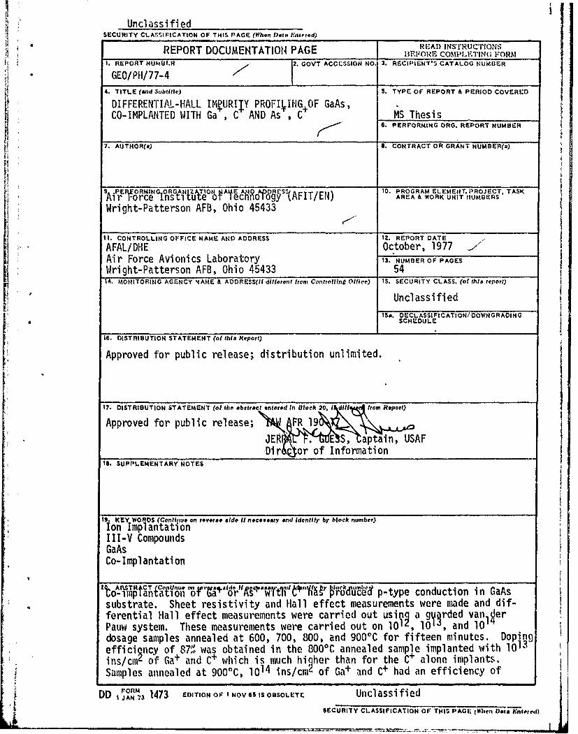
1. REPORT NUMAB.R 2, GOVT ACCLSSION NO. 3. RECIPIENT'S CATALOG NUMBER
GE/PH/77-44. TITLE (and Sbtitle) S. TYPE OF REPORT & PERIOD COVERED
DIFFERENTIAL-HALL IMtURIIY PROFIfING.OF GaAs,CO-IMPLANTED WITH Ga-, C AND As-, C' MS Thesis
6. PERFORMING ORG. REPORT NUMBER
7. AUTHOR(&) 8. CONTRACT OR GRANT NUMBER(a).
9 PEPJEORMINGGORGANIZATION I A , D S r 10. PROGRAM ELEMENT. PROJECT, TASK
Air Force instlltuve oT /ecnnoi o (AFIT/E'l) AREA & WORK UNIT NUMBERS
Wright-Patterson AFB, Ohio 45433
It. CONTROLLING OFFICE NAME AND ADDRESS 12. REPORT DATE
AFAL/DHE October, 1977 >'
Air Force Avionics Laboratory 3. NUMBER OF PAGES
Wright-Patterson AFB, Ohio 45433 5414. MONITORING AGENCY SAME & ADDRESS(II diferent from Controlling Office) IS. SECURITY CLASS. (of this repot)
Unclassified-I
I 15a. DECLASSIFICATION/DOWNGRADINGSCHEDULE
16. DISTRIBUTION STATEMENT (of this Report)
It Approved for public release; distribution unlimited.
17. DISTRIBUTION STATEMENT (of the abstract anered In Block 20, 1 i., l from, Report)
rel ase ";i "R 19 . . .I.Approved for public release; FR 19
JEFR tt~tE' Saptain, USAF-Di-r cor of Information
IS. SUPPLEMENTARY NOTES
19. KEY WORDS (Contiu'e on feverao aide II necesary) and Identify, by block number)Ion ImplantationIII-V CompoundsGaAsCo-Implantation
Zo- mpanlT aC on Ot i a-or 4A wrn han proaucd p-type conduction in GaAssubstrate. Sheet resistivity and Hall effect measurements were made and dif-ferential Hall effect measurements were carried out usi a gvrded vanperPauw system. These measurements were carried out on lO , 110,and 10dosage samples annealed at 600, 700, 800, and 9000C for fifteen minutes. Dopingefficiency of 87. was obtained in the 800
0C annealed sample implanted with 1013
ins/cm4 of Ga+ and C+ which is much hiqher than for the C+ alone implants.Samples annealed at 9000C, 1014 ins/cmL of Ga+ and C+ had an efficiency of
I FORM
DD I JAN73 1473 EDITION OF I NOV 6S IS OBSOLETE UnclassifiedSECURITY CLASSIFICATION OF THIS PAGE (Iten Data inltett)
UnclassifiedSECURITY CLASSIFICATION OF THIS PAGE(When DIat Ent red)
32.3' which is also higher than the C+ alone implants. Carboi implants alonehad a 57' efficiency when annealed at 9000C w th a dose of 10 3/cm4 and 9.5,'when annealed at 9000C with a dose of 10o14/cm, which verifies previous workdone with carbon implants.
Unclassified
SECURITY CLASSIrICATION OF THIS PAGEcW.o.tn :P.to 'ted)