8-bit c with 2/4/8k bytes in-systemww1.microchip.com/downloads/en/devicedoc/atmel... · pinout...
TRANSCRIPT

8-bit Microcontroller with 2/4/8K Bytes In-SystemProgrammable Flash
ATtiny261/V*ATtiny461/VATtiny861/V
*Mature
2588F–AVR–06/2013
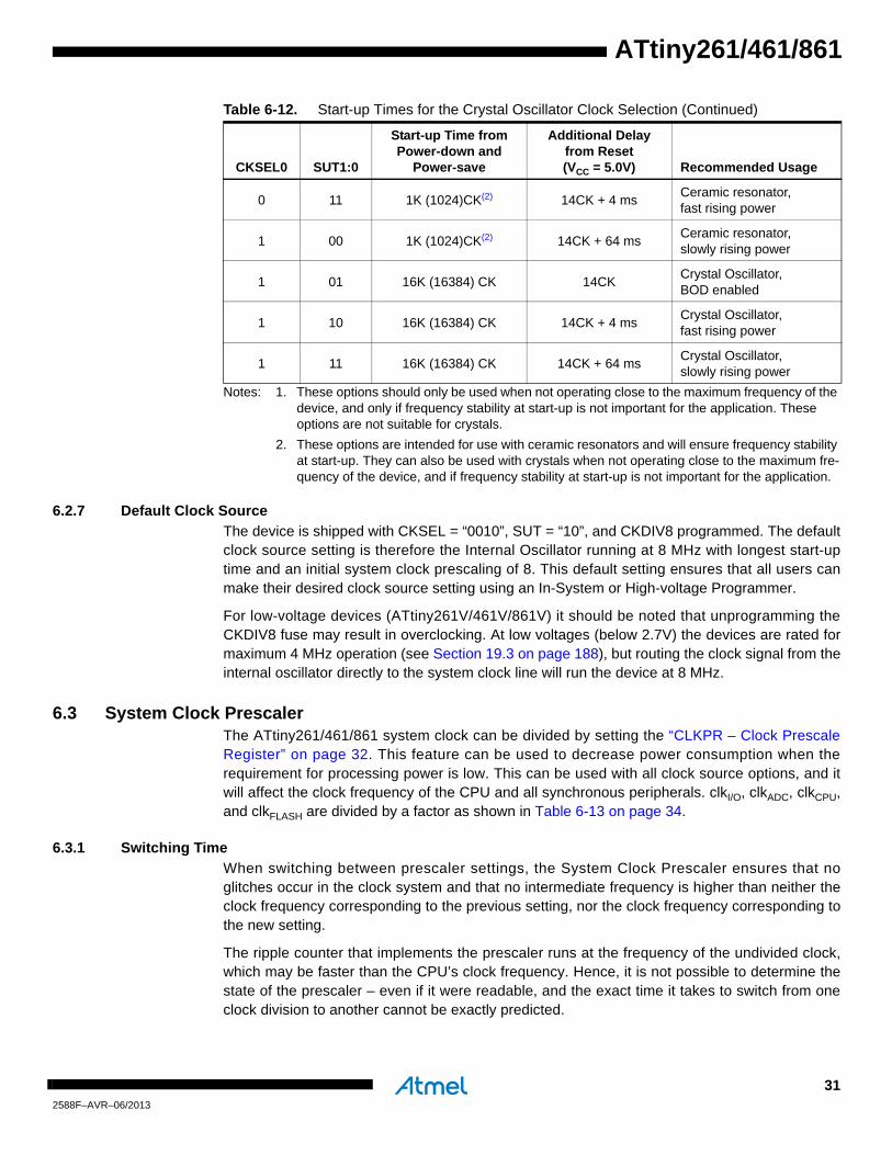
Features• High Performance, Low Power AVR® 8-Bit Microcontroller
• Advanced RISC Architecture
– 123 Powerful Instructions – Most Single Clock Cycle Execution
– 32 x 8 General Purpose Working Registers
– Fully Static Operation
• Non-volatile Program and Data Memories
– 2/4/8K Byte of In-System Programmable Program Memory Flash
• Endurance: 10,000 Write/Erase Cycles
– 128/256/512 Bytes In-System Programmable EEPROM
• Endurance: 100,000 Write/Erase Cycles
– 128/256/512 Bytes Internal SRAM
– Data retention: 20 years at 85°C / 100 years at 25C– Programming Lock for Self-Programming Flash Program & EEPROM Data Security
• Peripheral Features
– 8/16-bit Timer/Counter with Prescaler
– 8/10-bit High Speed Timer/Counter with Separate Prescaler
• 3 High Frequency PWM Outputs with Separate Output Compare Registers
• Programmable Dead Time Generator
– 10-bit ADC
• 11 Single-Ended Channels
• 16 Differential ADC Channel Pairs
• 15 Differential ADC Channel Pairs with Programmable Gain (1x, 8x, 20x, 32x)
– On-chip Analog Comparator
– Programmable Watchdog Timer with Separate On-chip Oscillator
– Universal Serial Interface with Start Condition Detector
• Special Microcontroller Features
– debugWIRE On-chip Debug System
– In-System Programmable via SPI Port
– External and Internal Interrupt Sources
– Low Power Idle, ADC Noise Reduction, Standby and Power-Down Modes
– Enhanced Power-on Reset Circuit
– Programmable Brown-out Detection Circuit
– Internal Calibrated Oscillator
– On-chip Temperature Sensor
• I/O and Packages
– 16 Programmable I/O Lines
– Available in 20-pin PDIP, 20-pin SOIC and 32-pad MLF
• Operating Voltage:
– 1.8 – 5.5V for ATtiny261V/461V/861V
– 2.7 – 5.5V for ATtiny261/461/861
• Speed Grade:
– ATtiny261V/461V/861V: 0 – 4 MHz @ 1.8 – 5.5V, 0 – 10 MHz @ 2.7 – 5.5V
– ATtiny261/461/861: 0 – 10 MHz @ 2.7 – 5.5V, 0 – 20 MHz @ 4.5 – 5.5V
• Industrial Temperature Range
• Low Power Consumption
– Active Mode (1 MHz System Clock): 300 µA @ 1.8V
– Power-Down Mode: 0.1 µA at 1.8V
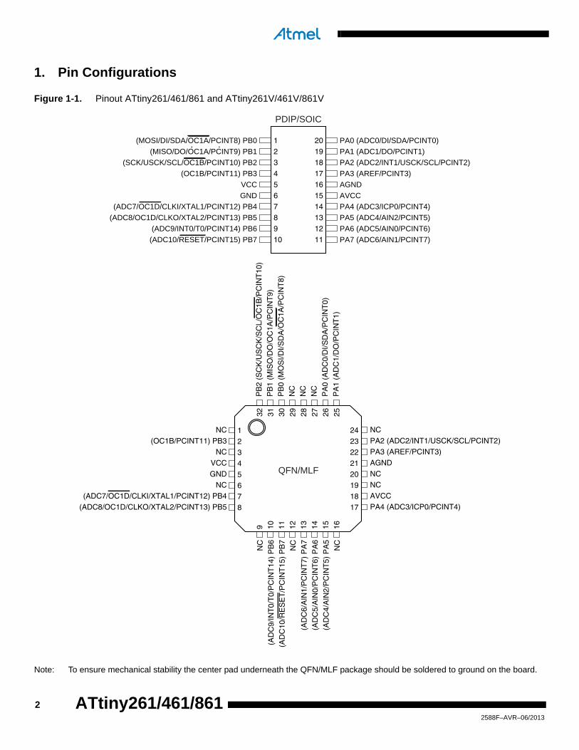
1. Pin Configurations
Figure 1-1. Pinout ATtiny261/461/861 and ATtiny261V/461V/861V
Note: To ensure mechanical stability the center pad underneath the QFN/MLF package should be soldered to ground on the board.
12345678910
20191817161514131211
(MOSI/DI/SDA/OC1A/PCINT8) PB0
(MISO/DO/OC1A/PCINT9) PB1
(SCK/USCK/SCL/OC1B/PCINT10) PB2
(OC1B/PCINT11) PB3
VCC
GND
(ADC7/OC1D/CLKI/XTAL1/PCINT12) PB4
(ADC8/OC1D/CLKO/XTAL2/PCINT13) PB5
(ADC9/INT0/T0/PCINT14) PB6
(ADC10/RESET/PCINT15) PB7
PA0 (ADC0/DI/SDA/PCINT0)
PA1 (ADC1/DO/PCINT1)
PA2 (ADC2/INT1/USCK/SCL/PCINT2)
PA3 (AREF/PCINT3)
AGND
AVCC
PA4 (ADC3/ICP0/PCINT4)
PA5 (ADC4/AIN2/PCINT5)
PA6 (ADC5/AIN0/PCINT6)
PA7 (ADC6/AIN1/PCINT7)
PDIP/SOIC
12345678
2423222120191817
32 31 30 29 28 27 26 25
9 10 11 12 13 14 15 16
NC(OC1B/PCINT11) PB3
NCVCCGND
NC(ADC7/OC1D/CLKI/XTAL1/PCINT12) PB4
(ADC8/OC1D/CLKO/XTAL2/PCINT13) PB5
NCPA2 (ADC2/INT1/USCK/SCL/PCINT2)PA3 (AREF/PCINT3)AGNDNCNCAVCCPA4 (ADC3/ICP0/PCINT4)
NC
(AD
C9/
INT
0/T
0/P
CIN
T14
) P
B6
(AD
C10
/RE
SE
T/P
CIN
T15
) P
B7
NC
(AD
C6/
AIN
1/P
CIN
T7)
PA
7 (
AD
C5/
AIN
0/P
CIN
T6)
PA
6(A
DC
4/A
IN2/
PC
INT
5) P
A5
NC
PB
2 (S
CK
/US
CK
/SC
L/O
C1B
/PC
INT
10)
PB
1 (M
ISO
/DO
/OC
1A/P
CIN
T9)
PB
0 (M
OS
I/DI/S
DA
/OC
1A/P
CIN
T8)
N
CN
CN
CP
A0
(AD
C0/
DI/S
DA
/PC
INT
0)P
A1
(AD
C1/
DO
/PC
INT
1)
QFN/MLF
22588F–AVR–06/2013
ATtiny261/461/861

ATtiny261/461/861
1.1 Pin Descriptions
1.1.1 VCC
Supply voltage.
1.1.2 GND
Ground.
1.1.3 AVCC
Analog supply voltage. This is the supply voltage pin for the Analog-to-digital Converter (ADC),the analog comparator, the Brown-Out Detector (BOD), the internal voltage reference and PortA. It should be externally connected to VCC, even if some peripherals such as the ADC are notused. If the ADC is used AVCC should be connected to VCC through a low-pass filter.
1.1.4 AGND
Analog ground.
1.1.5 Port A (PA7:PA0)
An 8-bit, bi-directional I/O port with internal pull-up resistors, individually selectable for each bit.Output buffers have symmetrical drive characteristics with both high sink and source capability.As inputs, port pins that are externally pulled low will source current if pull-up resistors havebeen activated. Port pins are tri-stated when a reset condition becomes active, even if the clockis not running.
Port A also serves the functions of various special features of the device, as listed on page 63.
1.1.6 Port B (PB7:PB0)
An 8-bit, bi-directional I/O port with internal pull-up resistors, individually selectable for each bit.Output buffers have symmetrical drive characteristics with both high sink and source capability.As inputs, port pins that are externally pulled low will source current if pull-up resistors havebeen activated. Port pins are tri-stated when a reset condition becomes active, even if the clockis not running.
Port B also serves the functions of various special features of the device, as listed on page 66.
1.1.7 RESET
Reset input. A low level on this pin for longer than the minimum pulse length will generate areset, even if the clock is not running and provided the reset pin has not been disabled. The min-imum pulse length is given in Table 19-4 on page 190. Shorter pulses are not guaranteed togenerate a reset.
The reset pin can also be used as a (weak) I/O pin.
32588F–AVR–06/2013

2. OverviewATtiny261/461/861 are low-power CMOS 8-bit microcontrollers based on the AVR enhancedRISC architecture. By executing powerful instructions in a single clock cycle, theATtiny261/461/861 achieves throughputs approaching 1 MIPS per MHz allowing the systemdesigner to optimize power consumption versus processing speed.
2.1 Block Diagram
Figure 2-1. Block Diagram
The AVR core combines a rich instruction set with 32 general purpose working registers. All 32registers are directly connected to the Arithmetic Logic Unit (ALU), allowing two independentregisters to be accessed in one single instruction executed in one clock cycle. The resultingarchitecture is more code efficient while achieving throughputs up to ten times faster than con-ventional CISC microcontrollers.
PORT A (8)PORT B (8)
USI
Timer/Counter1Timer/Counter0 A/D Conv.
InternalBandgap
Analog Comp.
SRAMFlash
EEPROM
WatchdogOscillator
WatchdogTimer
OscillatorCircuits /
ClockGeneration
PowerSupervisionPOR / BOD &
RESET
VC
C
GN
D
PROGRAMLOGIC
debugWIRE
AGND
AREF
AVCC
DAT
AB
US
PA[0..7]PB[0..7]
11
RESETXTAL[1..2]
CPU
3
42588F–AVR–06/2013
ATtiny261/461/861

ATtiny261/461/861
The ATtiny261/461/861 provides the following features: 2/4/8K byte of In-System ProgrammableFlash, 128/256/512 bytes EEPROM, 128/256/512 bytes SRAM, 16 general purpose I/O lines, 32general purpose working registers, an 8-bit Timer/Counter with compare modes, an 8-bit highspeed Timer/Counter, a Universal Serial Interface, Internal and External Interrupts, an 11-chan-nel, 10-bit ADC, a programmable Watchdog Timer with internal oscillator, and four softwareselectable power saving modes. Idle mode stops the CPU while allowing the SRAM,Timer/Counter, ADC, Analog Comparator, and Interrupt system to continue functioning. Power-down mode saves the register contents, disabling all chip functions until the next Interrupt orHardware Reset. ADC Noise Reduction mode stops the CPU and all I/O modules except ADC,to minimize switching noise during ADC conversions. In Standby mode, the crystal/resonatoroscillator is running while the rest of the device is sleeping, allowing very fast start-up combinedwith low power consumption.
The device is manufactured using Atmel’s high density non-volatile memory technology. TheOn-chip ISP Flash allows the Program memory to be re-programmed In-System through an SPIserial interface, by a conventional non-volatile memory programmer or by an On-chip boot coderunning on the AVR core.
The ATtiny261/461/861 AVR is supported by a full suite of program and system developmenttools including: C Compilers, Macro Assemblers, Program Debugger/Simulators, and Evaluationkits.
52588F–AVR–06/2013

3. About
3.1 ResourcesA comprehensive set of drivers, application notes, data sheets and descriptions on developmenttools are available for download at http://www.atmel.com/avr.
3.2 Code Examples This documentation contains simple code examples that briefly show how to use various parts ofthe device. These code examples assume that the part specific header file is included beforecompilation. Be aware that not all C compiler vendors include bit definitions in the header filesand interrupt handling in C is compiler dependent. Please confirm with the C compiler documen-tation for more details.
For I/O Registers located in the extended I/O map, “IN”, “OUT”, “SBIS”, “SBIC”, “CBI”, and “SBI”instructions must be replaced with instructions that allow access to extended I/O. Typically, thismeans “LDS” and “STS” combined with “SBRS”, “SBRC”, “SBR”, and “CBR”. Note that not allAVR devices include an extended I/O map.
3.3 Data RetentionReliability Qualification results show that the projected data retention failure rate is much lessthan 1 PPM over 20 years at 85°C or 100 years at 25°C.
3.4 DisclaimerTypical values contained in this data sheet are based on simulations and characterization ofother AVR microcontrollers manufactured on the same process technology.
62588F–AVR–06/2013
ATtiny261/461/861

ATtiny261/461/861
4. CPU CoreThis section discusses the AVR core architecture in general. The main function of the CPU coreis to ensure correct program execution. The CPU must therefore be able to access memories,perform calculations, control peripherals, and handle interrupts.
4.1 Architectural Overview
Figure 4-1. Block Diagram of the AVR Architecture
In order to maximize performance and parallelism, the AVR uses a Harvard architecture – withseparate memories and buses for program and data. Instructions in the Program memory areexecuted with a single level pipelining. While one instruction is being executed, the next instruc-tion is pre-fetched from the Program memory. This concept enables instructions to be executedin every clock cycle. The Program memory is In-System Reprogrammable Flash memory.
FlashProgramMemory
InstructionRegister
InstructionDecoder
ProgramCounter
Control Lines
32 x 8GeneralPurpose
Registrers
ALU
Statusand Control
I/O Lines
EEPROM
Data Bus 8-bit
DataSRAM
Dire
ct A
ddre
ssin
g
Indi
rect
Add
ress
ing
InterruptUnit
WatchdogTimer
AnalogComparator
I/O Module 2
I/O Module1
I/O Module n
72588F–AVR–06/2013

The fast-access Register File contains 32 x 8-bit general purpose working registers with a singleclock cycle access time. This allows single-cycle Arithmetic Logic Unit (ALU) operation. In a typ-ical ALU operation, two operands are output from the Register File, the operation is executed,and the result is stored back in the Register File – in one clock cycle.
Six of the 32 registers can be used as three 16-bit indirect address register pointers for DataSpace addressing – enabling efficient address calculations. One of the these address pointerscan also be used as an address pointer for look up tables in Flash Program memory. Theseadded function registers are the 16-bit X-, Y-, and Z-register, described later in this section.
The ALU supports arithmetic and logic operations between registers or between a constant anda register. Single register operations can also be executed in the ALU. After an arithmetic opera-tion, the Status Register is updated to reflect information about the result of the operation.
Program flow is provided by conditional and unconditional jump and call instructions, capable ofdirectly addressing the whole address space. Most AVR instructions have a single 16-bit wordformat but 32-bit wide instructions also exist. The actual instruction set varies, as some devicesonly implement a part of the instruction set.
During interrupts and subroutine calls, the return address Program Counter (PC) is stored on theStack. The Stack is effectively allocated in the general data SRAM, and consequently the Stacksize is only limited by the total SRAM size and the usage of the SRAM. All user programs mustinitialize the SP in the Reset routine (before subroutines or interrupts are executed). The StackPointer (SP) is read/write accessible in the I/O space. The data SRAM can easily be accessedthrough the five different addressing modes supported in the AVR architecture.
The memory spaces in the AVR architecture are all linear and regular memory maps.
A flexible interrupt module has its control registers in the I/O space with an additional GlobalInterrupt Enable bit in the Status Register. All interrupts have a separate Interrupt Vector in theInterrupt Vector table. The interrupts have priority in accordance with their Interrupt Vector posi-tion. The lower the Interrupt Vector address, the higher the priority.
The I/O memory space contains 64 addresses for CPU peripheral functions as Control Regis-ters, SPI, and other I/O functions. The I/O memory can be accessed directly, or as the DataSpace locations following those of the Register File, 0x20 - 0x5F.
4.2 ALU – Arithmetic Logic UnitThe high-performance AVR ALU operates in direct connection with all the 32 general purposeworking registers. Within a single clock cycle, arithmetic operations between general purposeregisters or between a register and an immediate are executed. The ALU operations are dividedinto three main categories – arithmetic, logical, and bit-functions. Some implementations of thearchitecture also provide a powerful multiplier supporting both signed/unsigned multiplicationand fractional format. See the “Instruction Set” section for a detailed description.
4.3 Status RegisterThe Status Register contains information about the result of the most recently executed arithme-tic instruction. This information can be used for altering program flow in order to performconditional operations. Note that the Status Register is updated after all ALU operations, asspecified in the Instruction Set Reference. This will in many cases remove the need for using thededicated compare instructions, resulting in faster and more compact code.
82588F–AVR–06/2013
ATtiny261/461/861

ATtiny261/461/861
The Status Register is neither automatically stored when entering an interrupt routine, norrestored when returning from an interrupt. This must be handled by software.
4.3.1 SREG – AVR Status Register
• Bit 7 – I: Global Interrupt Enable
The Global Interrupt Enable bit must be set for the interrupts to be enabled. The individual inter-rupt enable control is then performed in separate control registers. If the Global Interrupt EnableRegister is cleared, none of the interrupts are enabled independent of the individual interruptenable settings. The I-bit is cleared by hardware after an interrupt has occurred, and is set bythe RETI instruction to enable subsequent interrupts. The I-bit can also be set and cleared bythe application with the SEI and CLI instructions, as described in the instruction set reference.
• Bit 6 – T: Bit Copy Storage
The Bit Copy instructions BLD (Bit LoaD) and BST (Bit STore) use the T-bit as source or desti-nation for the operated bit. A bit from a register in the Register File can be copied into T by theBST instruction, and a bit in T can be copied into a bit in a register in the Register File by theBLD instruction.
• Bit 5 – H: Half Carry Flag
The Half Carry Flag H indicates a Half Carry in some arithmetic operations. Half Carry is usefulin BCD arithmetic. See the “Instruction Set Description” for detailed information.
• Bit 4 – S: Sign Bit, S = N V
The S-bit is always an exclusive or between the Negative Flag N and the Two’s ComplementOverflow Flag V. See the “Instruction Set Description” for detailed information.
• Bit 3 – V: Two’s Complement Overflow Flag
The Two’s Complement Overflow Flag V supports two’s complement arithmetics. See the“Instruction Set Description” for detailed information.
• Bit 2 – N: Negative Flag
The Negative Flag N indicates a negative result in an arithmetic or logic operation. See the“Instruction Set Description” for detailed information.
• Bit 1 – Z: Zero Flag
The Zero Flag Z indicates a zero result in an arithmetic or logic operation. See the “InstructionSet Description” for detailed information.
• Bit 0 – C: Carry Flag
The Carry Flag C indicates a carry in an arithmetic or logic operation. See the “Instruction SetDescription” for detailed information.
Bit 7 6 5 4 3 2 1 0
0x3F (0x5F) I T H S V N Z C SREG
Read/Write R/W R/W R/W R/W R/W R/W R/W R/W
Initial Value 0 0 0 0 0 0 0 0
92588F–AVR–06/2013
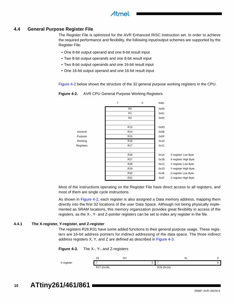
4.4 General Purpose Register FileThe Register File is optimized for the AVR Enhanced RISC instruction set. In order to achievethe required performance and flexibility, the following input/output schemes are supported by theRegister File:
• One 8-bit output operand and one 8-bit result input
• Two 8-bit output operands and one 8-bit result input
• Two 8-bit output operands and one 16-bit result input
• One 16-bit output operand and one 16-bit result input
Figure 4-2 below shows the structure of the 32 general purpose working registers in the CPU.
Figure 4-2. AVR CPU General Purpose Working Registers
Most of the instructions operating on the Register File have direct access to all registers, andmost of them are single cycle instructions.
As shown in Figure 4-2, each register is also assigned a Data memory address, mapping themdirectly into the first 32 locations of the user Data Space. Although not being physically imple-mented as SRAM locations, this memory organization provides great flexibility in access of theregisters, as the X-, Y- and Z-pointer registers can be set to index any register in the file.
4.4.1 The X-register, Y-register, and Z-register
The registers R26:R31 have some added functions to their general purpose usage. These regis-ters are 16-bit address pointers for indirect addressing of the data space. The three indirectaddress registers X, Y, and Z are defined as described in Figure 4-3.
Figure 4-3. The X-, Y-, and Z-registers
7 0 Addr.
R0 0x00
R1 0x01
R2 0x02
…
R13 0x0D
General R14 0x0E
Purpose R15 0x0F
Working R16 0x10
Registers R17 0x11
…
R26 0x1A X-register Low Byte
R27 0x1B X-register High Byte
R28 0x1C Y-register Low Byte
R29 0x1D Y-register High Byte
R30 0x1E Z-register Low Byte
R31 0x1F Z-register High Byte
15 XH XL 0
X-register 7 0 7 0
R27 (0x1B) R26 (0x1A)
102588F–AVR–06/2013
ATtiny261/461/861

ATtiny261/461/861
In different addressing modes these address registers function as automatic increment andautomatic decrement (see the instruction set reference for details).
4.5 Stack PointerThe Stack is mainly used for storing temporary data, for storing local variables and for storingreturn addresses after interrupts and subroutine calls. The Stack Pointer Register always pointsto the top of the Stack. Note that the Stack is implemented as growing from higher memory loca-tions to lower memory locations. This implies that a Stack PUSH command decreases the StackPointer.
The Stack Pointer points to the data SRAM Stack area where the Subroutine and InterruptStacks are located. This Stack space in the data SRAM must be defined by the program beforeany subroutine calls are executed or interrupts are enabled. The Stack Pointer must be set topoint above 0x60. The Stack Pointer is decremented by one when data is pushed onto the Stackwith the PUSH instruction, and it is decremented by two when the return address is pushed ontothe Stack with subroutine call or interrupt. The Stack Pointer is incremented by one when data ispopped from the Stack with the POP instruction, and it is incremented by two when data ispopped from the Stack with return from subroutine RET or return from interrupt RETI.
The AVR Stack Pointer is implemented as two 8-bit registers in the I/O space. The number ofbits actually used is implementation dependent. Note that the data space in some implementa-tions of the AVR architecture is so small that only SPL is needed. In this case, the SPH Registerwill not be present
4.5.1 SPH and SPL — Stack Pointer Register
4.6 Instruction Execution TimingThis section describes the general access timing concepts for instruction execution. The AVRCPU is driven by the CPU clock clkCPU, directly generated from the selected clock source for thechip. No internal clock division is used.
Figure 4-4 shows the parallel instruction fetches and instruction executions enabled by the Har-vard architecture and the fast access Register File concept. This is the basic pipelining conceptto obtain up to 1 MIPS per MHz with the corresponding unique results for functions per cost,functions per clocks, and functions per power-unit.
15 YH YL 0
Y-register 7 0 7 0
R29 (0x1D) R28 (0x1C)
15 ZH ZL 0
Z-register 7 0 7 0
R31 (0x1F) R30 (0x1E)
Bit 15 14 13 12 11 10 9 8
0x3E (0x5E) SP15 SP14 SP13 SP12 SP11 SP10 SP9 SP8 SPH
0x3D (0x5D) SP7 SP6 SP5 SP4 SP3 SP2 SP1 SP0 SPL
7 6 5 4 3 2 1 0
Read/Write R/W R/W R/W R/W R/W R/W R/W R/W
R/W R/W R/W R/W R/W R/W R/W R/W
Initial Value RAMEND RAMEND RAMEND RAMEND RAMEND RAMEND RAMEND RAMEND
RAMEND RAMEND RAMEND RAMEND RAMEND RAMEND RAMEND RAMEND
112588F–AVR–06/2013

Figure 4-4. The Parallel Instruction Fetches and Instruction Executions
Figure 4-5 shows the internal timing concept for the Register File. In a single clock cycle an ALUoperation using two register operands is executed, and the result is stored back to the destina-tion register.
Figure 4-5. Single Cycle ALU Operation
4.7 Reset and Interrupt HandlingThe AVR provides several different interrupt sources. These interrupts and the separate ResetVector each have a separate Program Vector in the Program memory space. All interrupts areassigned individual enable bits which must be written logic one together with the Global InterruptEnable bit in the Status Register in order to enable the interrupt.
The lowest addresses in the Program memory space are by default defined as the Reset andInterrupt Vectors. The complete list of vectors is shown in “Interrupts” on page 50. The list alsodetermines the priority levels of the different interrupts. The lower the address the higher is thepriority level. RESET has the highest priority, and next is INT0 – the External Interrupt Request0.
When an interrupt occurs, the Global Interrupt Enable I-bit is cleared and all interrupts are dis-abled. The user software can write logic one to the I-bit to enable nested interrupts. All enabledinterrupts can then interrupt the current interrupt routine. The I-bit is automatically set when aReturn from Interrupt instruction – RETI – is executed.
There are basically two types of interrupts. The first type is triggered by an event that sets theInterrupt Flag. For these interrupts, the Program Counter is vectored to the actual Interrupt Vec-tor in order to execute the interrupt handling routine, and hardware clears the correspondingInterrupt Flag. Interrupt Flags can also be cleared by writing a logic one to the flag bit position(s)
clk
1st Instruction Fetch
1st Instruction Execute2nd Instruction Fetch
2nd Instruction Execute3rd Instruction Fetch
3rd Instruction Execute4th Instruction Fetch
T1 T2 T3 T4
CPU
Total Execution Time
Register Operands Fetch
ALU Operation Execute
Result Write Back
T1 T2 T3 T4
clkCPU
122588F–AVR–06/2013
ATtiny261/461/861
ATtiny261/461/861
to be cleared. If an interrupt condition occurs while the corresponding interrupt enable bit iscleared, the Interrupt Flag will be set and remembered until the interrupt is enabled, or the flag iscleared by software. Similarly, if one or more interrupt conditions occur while the Global InterruptEnable bit is cleared, the corresponding Interrupt Flag(s) will be set and remembered until theGlobal Interrupt Enable bit is set, and will then be executed by order of priority.
The second type of interrupts will trigger as long as the interrupt condition is present. Theseinterrupts do not necessarily have Interrupt Flags. If the interrupt condition disappears before theinterrupt is enabled, the interrupt will not be triggered.
When the AVR exits from an interrupt, it will always return to the main program and execute onemore instruction before any pending interrupt is served.
Note that the Status Register is not automatically stored when entering an interrupt routine, norrestored when returning from an interrupt routine. This must be handled by software.
When using the CLI instruction to disable interrupts, the interrupts will be immediately disabled.No interrupt will be executed after the CLI instruction, even if it occurs simultaneously with theCLI instruction. The following example shows how this can be used to avoid interrupts during thetimed EEPROM write sequence.
Note: See “Code Examples” on page 6.
When using the SEI instruction to enable interrupts, the instruction following SEI will be exe-cuted before any pending interrupts, as shown in the following examples.
Assembly Code Example
in r16, SREG ; store SREG value
cli ; disable interrupts during timed sequence
sbi EECR, EEMPE ; start EEPROM write
sbi EECR, EEPE
out SREG, r16 ; restore SREG value (I-bit)
C Code Example
char cSREG;
cSREG = SREG; /* store SREG value */
/* disable interrupts during timed sequence */
_CLI();
EECR |= (1<<EEMPE); /* start EEPROM write */
EECR |= (1<<EEPE);
SREG = cSREG; /* restore SREG value (I-bit) */
Assembly Code Example
sei ; set Global Interrupt Enable
sleep ; enter sleep, waiting for interrupt
; note: will enter sleep before any pending interrupt(s)
132588F–AVR–06/2013

Note: See “Code Examples” on page 6.
4.7.1 Interrupt Response Time
The interrupt execution response for all the enabled AVR interrupts is four clock cycles mini-mum. After four clock cycles the Program Vector address for the actual interrupt handling routineis executed. During this four clock cycle period, the Program Counter is pushed onto the Stack.The vector is normally a jump to the interrupt routine, and this jump takes three clock cycles. Ifan interrupt occurs during execution of a multi-cycle instruction, this instruction is completedbefore the interrupt is served. If an interrupt occurs when the MCU is in sleep mode, the interruptexecution response time is increased by four clock cycles. This increase comes in addition to thestart-up time from the selected sleep mode.
A return from an interrupt handling routine takes four clock cycles. During these four clockcycles, the Program Counter (two bytes) is popped back from the Stack, the Stack Pointer isincremented by two, and the I-bit in SREG is set.
C Code Example
_SEI(); /* set Global Interrupt Enable */
_SLEEP(); /* enter sleep, waiting for interrupt */
/* note: will enter sleep before any pending interrupt(s) */
142588F–AVR–06/2013
ATtiny261/461/861

ATtiny261/461/861
5. MemoriesThis section describes the different memories in the ATtiny261/461/861. The AVR architecturehas two main memory spaces, the Data memory and the Program memory space. In addition,the ATtiny261/461/861 features an EEPROM Memory for data storage. All three memoryspaces are linear and regular.
5.1 In-System Re-programmable Flash Program Memory The ATtiny261/461/861 contains 2/4/8K byte On-chip In-System Reprogrammable Flash mem-ory for program storage. Since all AVR instructions are 16 or 32 bits wide, the Flash is organizedas 1024/2048/4096 x 16.
The Flash memory has an endurance of at least 10,000 wri te/erase cycles. TheATtiny261/461/861 Program Counter (PC) is 10/11/12 bits wide, thus capable of addressing the1024/2048/4096 Program memory locations. “Memory Programming” on page 170 contains adetailed description on Flash data serial downloading using the SPI pins.
Constant tables can be allocated within the entire address space of program memory (see theLPM – Load Program memory instruction description).
Timing diagrams for instruction fetch and execution are presented in “Instruction Execution Tim-ing” on page 11.
Figure 5-1. Program Memory Map
5.2 SRAM Data MemoryFigure 5-2 on page 16 shows how the ATtiny261/461/861 SRAM Memory is organized.
The lower data memory locations address both the Register File, the I/O memory and the inter-nal data SRAM. The first 32 locations address the Register File, the next 64 locations thestandard I/O memory, and the last 128/256/512 locations address the internal data SRAM.
The five different addressing modes for the Data memory cover: Direct, Indirect with Displace-ment, Indirect, Indirect with Pre-decrement, and Indirect with Post-increment. In the RegisterFile, registers R26 to R31 feature the indirect addressing pointer registers.
The direct addressing reaches the entire data space.
The Indirect with Displacement mode reaches 63 address locations from the base address givenby the Y- or Z-register.
0x0000
0x03FF/0x07FF/0x0FFF
Program Memory
152588F–AVR–06/2013

When using register indirect addressing modes with automatic pre-decrement and post-incre-ment, the address registers X, Y, and Z are decremented or incremented.
The 32 general purpose working registers, 64 I/O Registers, and the 128/256/512 bytes of inter-nal data SRAM in the ATtiny261/461/861 are all accessible through all these addressing modes.The Register File is described in “General Purpose Register File” on page 10.
Figure 5-2. Data Memory Map
5.2.1 Data Memory Access Times
This section describes the general access timing concepts for internal memory access. Theinternal data SRAM access is performed in two clkCPU cycles as illustrated in Figure 5-3.
Figure 5-3. On-chip Data SRAM Access Cycles
5.3 EEPROM Data MemoryThe ATtiny261/461/861 contains 128/256/512 bytes of data EEPROM memory. It is organizedas a separate data space, in which single bytes can be read and written. The EEPROM has anendurance of at least 100,000 write/erase cycles. The access between the EEPROM and theCPU is described in the following, specifying the EEPROM Address Registers, the EEPROMData Register, and the EEPROM Control Register. For a detailed description of Serial datadownloading to the EEPROM, see “Electrical Characteristics” on page 187.
32 Registers64 I/O Registers
Internal SRAM(128/256/512 x 8)
0x0000 - 0x001F0x0020 - 0x005F
0x0DF/0x15F/0x25F
0x0060
Data Memory
clk
WR
RD
Data
Data
Address Address valid
T1 T2 T3
Compute Address
Rea
dW
rite
CPU
Memory Access Instruction Next Instruction
162588F–AVR–06/2013
ATtiny261/461/861

ATtiny261/461/861
5.3.1 EEPROM Read/Write Access
The EEPROM Access Registers are accessible in the I/O space.
The write access times for the EEPROM are given in Table 5-1 on page 22. A self-timing func-tion, however, lets the user software detect when the next byte can be written. If the user codecontains instructions that write the EEPROM, some precautions must be taken. In heavily fil-tered power supplies, VCC is likely to rise or fall slowly on Power-up/down. This causes thedevice for some period of time to run at a voltage lower than specified as minimum for the clockfrequency used. See “Preventing EEPROM Corruption” on page 19 for details on how to avoidproblems in these situations.
In order to prevent unintentional EEPROM writes, a specific write procedure must be followed.Refer to “Atomic Byte Programming” on page 17 and “Split Byte Programming” on page 17 fordetails on this.
When the EEPROM is read, the CPU is halted for four clock cycles before the next instruction isexecuted. When the EEPROM is written, the CPU is halted for two clock cycles before the nextinstruction is executed.
5.3.2 Atomic Byte Programming
Using Atomic Byte Programming is the simplest mode. When writing a byte to the EEPROM, theuser must write the address into the EEARL Register and data into EEDR Register. If theEEPMn bits are zero, writing EEPE (within four cycles after EEMPE is written) will trigger theerase/write operation. Both the erase and write cycle are done in one operation and the totalprogramming time is given in Table 5-1 on page 22. The EEPE bit remains set until the eraseand write operations are completed. While the device is busy with programming, it is not possi-ble to do any other EEPROM operations.
5.3.3 Split Byte Programming
It is possible to split the erase and write cycle in two different operations. This may be useful ifthe system requires short access time for some limited period of time (typically if the power sup-ply voltage falls). In order to take advantage of this method, it is required that the locations to bewritten have been erased before the write operation. But since the erase and write operationsare split, it is possible to do the erase operations when the system allows doing time-criticaloperations (typically after Power-up).
5.3.4 Erase
To erase a byte, the address must be written to EEAR. If the EEPMn bits are 0b01, writing theEEPE within four cycles after EEMPE is written will trigger the erase operation only (program-ming time is given in Table 5-1 on page 22). The EEPE bit remains set until the erase operationcompletes. While the device is busy programming, it is not possible to do any other EEPROMoperations.
5.3.5 Write
To write a location, the user must write the address into EEAR and the data into EEDR. If theEEPMn bits are 0b10, writing the EEPE (within four cycles after EEMPE is written) will triggerthe write operation only (programming time is given in Table 5-1 on page 22). The EEPE bitremains set until the write operation completes. If the location to be written has not been erasedbefore write, the data that is stored must be considered as lost. While the device is busy withprogramming, it is not possible to do any other EEPROM operations.
172588F–AVR–06/2013

The calibrated Oscillator is used to time the EEPROM accesses. Make sure the Oscillator fre-quency is within the requirements described in “OSCCAL – Oscillator Calibration Register” onpage 32.
5.3.6 Program Examples
The following code examples show one assembly and one C function for erase, write, or atomicwrite of the EEPROM. The examples assume that interrupts are controlled (e.g., by disablinginterrupts globally) so that no interrupts will occur during execution of these functions.
Note: See “Code Examples” on page 6.
Assembly Code Example
EEPROM_write:
; Wait for completion of previous write
sbic EECR,EEPE
rjmp EEPROM_write
; Set Programming mode
ldi r16, (0<<EEPM1)|(0<<EEPM0)
out EECR, r16
; Set up address (r18:r17) in address register
out EEARH, r18
out EEARL, r17
; Write data (r19) to data register
out EEDR, r19
; Write logical one to EEMPE
sbi EECR,EEMPE
; Start eeprom write by setting EEPE
sbi EECR,EEPE
ret
C Code Example
void EEPROM_write(unsigned char ucAddress, unsigned char ucData)
{
/* Wait for completion of previous write */
while(EECR & (1<<EEPE))
;
/* Set Programming mode */
EECR = (0<<EEPM1)|(0<<EEPM0);
/* Set up address and data registers */
EEAR = ucAddress;
EEDR = ucData;
/* Write logical one to EEMPE */
EECR |= (1<<EEMPE);
/* Start eeprom write by setting EEPE */
EECR |= (1<<EEPE);
}
182588F–AVR–06/2013
ATtiny261/461/861

ATtiny261/461/861
The next code examples show assembly and C functions for reading the EEPROM. The exam-ples assume that interrupts are controlled so that no interrupts will occur during execution ofthese functions.
Note: See “Code Examples” on page 6.
5.3.7 Preventing EEPROM Corruption
During periods of low VCC, the EEPROM data can be corrupted because the supply voltage istoo low for the CPU and the EEPROM to operate properly. These issues are the same as forboard level systems using EEPROM, and the same design solutions should be applied.
An EEPROM data corruption can be caused by two situations when the voltage is too low. First,a regular write sequence to the EEPROM requires a minimum voltage to operate correctly. Sec-ondly, the CPU itself can execute instructions incorrectly, if the supply voltage is too low.
EEPROM data corruption can easily be avoided by following this design recommendation:
Keep the AVR RESET active (low) during periods of insufficient power supply voltage. This canbe done by enabling the internal Brown-out Detector (BOD). If the detection level of the internalBOD does not match the needed detection level, an external low VCC reset protection circuit can
Assembly Code Example
EEPROM_read:
; Wait for completion of previous write
sbic EECR,EEPE
rjmp EEPROM_read
; Set up address (r18:r17) in address register
out EEARH, r18
out EEARL, r17
; Start eeprom read by writing EERE
sbi EECR,EERE
; Read data from data register
in r16,EEDR
ret
C Code Example
unsigned char EEPROM_read(unsigned char ucAddress)
{
/* Wait for completion of previous write */
while(EECR & (1<<EEPE))
;
/* Set up address register */
EEAR = ucAddress;
/* Start eeprom read by writing EERE */
EECR |= (1<<EERE);
/* Return data from data register */
return EEDR;
}
192588F–AVR–06/2013

be used. If a reset occurs while a write operation is in progress, the write operation will be com-pleted provided that the power supply voltage is sufficient.
5.4 I/O MemoryThe I/O space definition of the ATtiny261/461/861 is shown in “Register Summary” on page 223.
All ATtiny261/461/861 I/Os and peripherals are placed in the I/O space. All I/O locations may beaccessed using the LD/LDS/LDD and ST/STS/STD instructions, enabling data transfer betweenthe 32 general purpose working registers and the I/O space. I/O Registers within the addressrange 0x00 - 0x1F are directly bit-accessible using the SBI and CBI instructions. In these regis-ters, the value of single bits can be checked by using the SBIS and SBIC instructions. Refer tothe instruction set section for more details. When using the I/O specific commands IN and OUT,the I/O addresses 0x00 - 0x3F must be used. When addressing I/O Registers as data spaceusing LD and ST instructions, 0x20 must be added to these addresses.
For compatibility with future devices, reserved bits should be written to zero if accessed.Reserved I/O memory addresses should never be written.
Some of the Status Flags are cleared by writing a logical one to them. Note that, the CBI andSBI instructions will only operate on the specified bit, and can therefore be used on registerscontaining such Status Flags. The CBI and SBI instructions work on registers in the addressrange 0x00 to 0x1F, only.
The I/O and Peripherals Control Registers are explained in later sections.
5.4.1 General Purpose I/O Registers
The ATtiny261/461/861 contains three General Purpose I/O Registers. These registers can beused for storing any information, and they are particularly useful for storing global variables andStatus Flags. General Purpose I/O Registers within the address range 0x00 - 0x1F are directlybit-accessible using the SBI, CBI, SBIS, and SBIC instructions.
5.5 Register Description
5.5.1 EEARH – EEPROM Address Register
• Bits 7:1 – Res: Reserved Bits
These bits are reserved and will always read as zero.
• Bit 0 – EEAR8: EEPROM Address
This is the most significant EEPROM address bit of ATtiny861. In devices with less EEPROM,i.e. ATtiny261/ATtiny461, this bit is reserved and will always read zero. The initial value of theEEPROM Address Register (EEAR) is undefined and a proper value must therefore be writtenbefore the EEPROM is accessed.
Bit 7 6 5 4 3 2 1 0
0x1F (0x3F) – – – – – – – EEAR8 EEARH
Read/Write R R R R R R R R/W
Initial Value 0 0 0 0 0 0 0 X/0
202588F–AVR–06/2013
ATtiny261/461/861

ATtiny261/461/861
5.5.2 EEARL – EEPROM Address Register
• Bit 7 – EEAR7: EEPROM Address
This is the most significant EEPROM address bit of ATtiny461. In devices with less EEPROM,i.e. ATtiny261, this bit is reserved and will always read zero. The initial value of the EEPROMAddress Register (EEAR) is undefined and a proper value must therefore be written before theEEPROM is accessed.
• Bits 6:0 – EEAR6:0: EEPROM Address
These are the (low) bits of the EEPROM Address Register. The EEPROM data bytes areaddressed linearly in the range 0...128/256/512. The initial value of EEAR is undefined and aproper value must be therefore be written before the EEPROM may be accessed.
5.5.3 EEDR – EEPROM Data Register
• Bits 7:0 – EEDR7:0: EEPROM Data
For the EEPROM write operation the EEDR Register contains the data to be written to theEEPROM in the address given by the EEAR Register. For the EEPROM read operation, theEEDR contains the data read out from the EEPROM at the address given by EEAR.
5.5.4 EECR – EEPROM Control Register
• Bit 7 – Res: Reserved Bit
This bit is reserved for future use and will always read as 0 in ATtiny261/461/861. For compati-bility with future AVR devices, always write this bit to zero. After reading, mask out this bit.
• Bit 6 – Res: Reserved Bit
This bit is reserved in the ATtiny261/461/861 and will always read as zero.
• Bits 5, 4 – EEPM1 and EEPM0: EEPROM Programming Mode Bits
The EEPROM Programming mode bits setting defines which programming action that will betriggered when writing EEPE. It is possible to program data in one atomic operation (erase the
Bit 7 6 5 4 3 2 1 0
0x1E (0x3E) EEAR7 EEAR6 EEAR5 EEAR4 EEAR3 EEAR2 EEAR1 EEAR0 EEARL
Read/Write R/W R/W R/W R/W R/W R/W R/W R/W
Initial Value X/0 X X X X X X X
Bit 7 6 5 4 3 2 1 0
0x1D (0x3D) EEDR7 EEDR6 EEDR5 EEDR4 EEDR3 EEDR2 EEDR1 EEDR0 EEDR
Read/Write R/W R/W R/W R/W R/W R/W R/W R/W
Initial Value 0 0 0 0 0 0 0 0
Bit 7 6 5 4 3 2 1 0
0x1C (0x3C) – – EEPM1 EEPM0 EERIE EEMPE EEPE EERE EECR
Read/Write R R R/W R/W R/W R/W R/W R/W
Initial Value 0 0 X X 0 0 X 0
212588F–AVR–06/2013

old value and program the new value) or to split the Erase and Write operations in two differentoperations. The Programming times for the different modes are shown in Table 5-1.
When EEPE is set, any write to EEPMn will be ignored. During reset, the EEPMn bits will bereset to 0b00 unless the EEPROM is busy programming.
• Bit 3 – EERIE: EEPROM Ready Interrupt Enable
Writing EERIE to one enables the EEPROM Ready Interrupt if the I-bit in SREG is set. WritingEERIE to zero disables the interrupt. The EEPROM Ready Interrupt generates a constant inter-rupt when Non-volatile memory is ready for programming.
• Bit 2 – EEMPE: EEPROM Master Program Enable
The EEMPE bit determines whether writing EEPE to one will have effect or not.
When EEMPE is set, setting EEPE within four clock cycles will program the EEPROM at theselected address. If EEMPE is zero, setting EEPE will have no effect. When EEMPE has beenwritten to one by software, hardware clears the bit to zero after four clock cycles.
• Bit 1 – EEPE: EEPROM Program Enable
The EEPROM Program Enable Signal EEPE is the programming enable signal to the EEPROM.When EEPE is written, the EEPROM will be programmed according to the EEPMn bits setting.The EEMPE bit must be written to one before a logical one is written to EEPE, otherwise noEEPROM write takes place. When the write access time has elapsed, the EEPE bit is clearedby hardware. When EEPE has been set, the CPU is halted for two cycles before the nextinstruction is executed.
• Bit 0 – EERE: EEPROM Read Enable
The EEPROM Read Enable Signal – EERE – is the read strobe to the EEPROM. When the cor-rect address is set up in the EEAR Register, the EERE bit must be written to one to trigger theEEPROM read. The EEPROM read access takes one instruction, and the requested data isavailable immediately. When the EEPROM is read, the CPU is halted for four cycles before thenext instruction is executed. The user should poll the EEPE bit before starting the read opera-tion. If a write operation is in progress, it is neither possible to read the EEPROM, nor to changethe EEAR Register.
5.5.5 GPIOR2 – General Purpose I/O Register 2
Table 5-1. EEPROM Mode Bits
EEPM1 EEPM0Programming
Time Operation
0 0 3.4 ms Erase and Write in one operation (Atomic Operation)
0 1 1.8 ms Erase Only
1 0 1.8 ms Write Only
1 1 – Reserved for future use
Bit 7 6 5 4 3 2 1 0
0x0C (0x2C) MSB LSB GPIOR2
Read/Write R/W R/W R/W R/W R/W R/W R/W R/W
Initial Value 0 0 0 0 0 0 0 0
222588F–AVR–06/2013
ATtiny261/461/861

ATtiny261/461/861
5.5.6 GPIOR1 – General Purpose I/O Register 1
5.5.7 GPIOR0 – General Purpose I/O Register 0
Bit 7 6 5 4 3 2 1 0
0x0B (0x2B) MSB LSB GPIOR1
Read/Write R/W R/W R/W R/W R/W R/W R/W R/W
Initial Value 0 0 0 0 0 0 0 0
Bit 7 6 5 4 3 2 1 0
0x0A (0x2A) MSB LSB GPIOR0
Read/Write R/W R/W R/W R/W R/W R/W R/W R/W
Initial Value 0 0 0 0 0 0 0 0
232588F–AVR–06/2013

6. Clock SystemFigure 6-1 presents the principal clock systems and their distribution in ATtiny261/461/861. All ofthe clocks need not be active at a given time. In order to reduce power consumption, the clocksto modules not being used can be halted by using different sleep modes, as described in “PowerManagement and Sleep Modes” on page 36.
Figure 6-1. Clock Distribution
6.1 Clock SubsystemsThe clock subsystems are detailed in the sections below.
6.1.1 CPU Clock – clkCPU
The CPU clock is routed to parts of the system concerned with operation of the AVR core.Examples of such modules are the General Purpose Register File, the Status Register and theData memory holding the Stack Pointer. Halting the CPU clock inhibits the core from performinggeneral operations and calculations.
6.1.2 I/O Clock – clkI/O
The I/O clock is used by the majority of the I/O modules, like Timer/Counter. The I/O clock isalso used by the External Interrupt module, but note that some external interrupts are detectedby asynchronous logic, allowing such interrupts to be detected even if the I/O clock is halted.
General I/OModules
CPU Core RAM
clkI/O AVR ClockControl Unit
clkCPU
Flash andEEPROM
clkFLASH
Source clock
Watchdog Timer
WatchdogOscillator
Reset Logic
ClockMultiplexer
Watchdog clock
Calibrated RCOscillator
Calibrated RCOscillator
ADC
clkADC
CrystalOscillator
Low-FrequencyCrystal Oscillator
System ClockPrescaler
PLLOscillator
clkPCK
General I/OModules
External Clock
clkPLL
242588F–AVR–06/2013
ATtiny261/461/861

ATtiny261/461/861
6.1.3 Flash Clock – clkFLASH
The Flash clock controls operation of the Flash interface. The Flash clock is usually active simul-taneously with the CPU clock.
6.1.4 ADC Clock – clkADC
The ADC is provided with a dedicated clock domain. This allows halting the CPU and I/O clocksin order to reduce noise generated by digital circuitry. This gives more accurate ADC conversionresults.
6.1.5 Fast Peripheral Clock – clkPCK
Selected peripherals can be clocked at a frequency higher than the CPU core. The fast periph-eral clock is generated by an on-chip PLL circuit.
6.1.6 PLL System Clock – clkADC
The PLL can also be used to generate a system clock. The clock signal can be prescaled toavoid overclocking the CPU.
6.2 Clock SourcesThe device has the following clock source options, selectable by Flash Fuse bits as shownbelow. The clock from the selected source is input to the AVR clock generator, and routed to theappropriate modules.
Note: 1. For all fuses “1” means unprogrammed and “0” means programmed.
The various choices for each clocking option is given in the following sections. When the CPUwakes up from Power-down or Power-save, the selected clock source is used to time the start-up, ensuring stable oscillator operation before instruction execution starts. When the CPU startsfrom reset, there is an additional delay allowing the power to reach a stable level before com-
Table 6-1. Device Clocking Options Select(1) vs. PB4 and PB5 Functionality
Device Clocking Option CKSEL3:0 PB4 PB5
External Clock (see page 26) 0000 XTAL1 I/O
High-Frequency PLL Clock (see page 26) 0001 I/O I/O
Calibrated Internal 8 MHz Oscillator (see page 28) 0010 I/O I/O
Internal 128 kHz Oscillator (see page 29) 0011 I/O I/O
Low-Frequency Crystal Oscillator (see page 29) 01xx XTAL1 XTAL2
Crystal Oscillator / Ceramic Resonator0.4...0.9 MHz (see page 30)
10001001
XTAL1 XTAL2
Crystal Oscillator / Ceramic Resonator0.9...3.0 MHz (see page 30)
10101011
XTAL1 XTAL2
Crystal Oscillator / Ceramic Resonator3...8 MHz (see page 30)
11001101
XTAL1 XTAL2
Crystal Oscillator / Ceramic Resonator8...20 MHz (see page 30)
11101111
XTAL1 XTAL2
252588F–AVR–06/2013

mencing normal operation. The watchdog oscillator is used for timing this real-time part of thestart-up time. The number of WD oscillator cycles used for each time-out is shown in Table 6-2.
6.2.1 External Clock
To drive the device from an external clock source, CLKI should be driven as shown in Figure 6-2. To run the device on an external clock, the CKSEL Fuses must be programmed to “0000”.
Figure 6-2. External Clock Drive Configuration
When this clock source is selected, start-up times are determined by the SUT Fuses as shown inTable 6-3.
When applying an external clock, it is required to avoid sudden changes in the applied clock fre-quency to ensure stable operation of the MCU. A variation in frequency of more than 2% fromone clock cycle to the next can lead to unpredictable behavior. It is required to ensure that theMCU is kept in Reset during such changes in the clock frequency.
Note that the system clock prescaler can be used to implement run-time changes of the internalclock frequency. See “System Clock Prescaler” on page 31 for details.
6.2.2 High-Frequency PLL Clock
The internal PLL generates a clock signal with a frequency eight times higher than the sourceinput. The PLL uses the output of the internal 8 MHz oscillator as source and the default settinggenerates a fast peripheral clock signal of 64 MHz.
Table 6-2. Number of Watchdog Oscillator Cycles
Typ Time-out Number of Cycles
4 ms 512
64 ms 8K (8,192)
Table 6-3. Start-up Times for the External Clock Selection
SUT1:0Start-up Time from Power-
down and Power-saveAdditional Delay from
Reset Recommended Usage
00 6 CK 14CK BOD enabled
01 6 CK 14CK + 4 ms Fast rising power
10 6 CK 14CK + 64 ms Slowly rising power
11 Reserved
EXTERNALCLOCKSIGNAL
CLKI
GND
262588F–AVR–06/2013
ATtiny261/461/861

ATtiny261/461/861
The fast peripheral clock, clkPCK, can be selected as the clock source for Timer/Counter1 and aprescaled version of the PLL output, clkPLL, can be selected as system clock. See Figure 6-3 fora detailed illustration on the PLL clock system.
Figure 6-3. PCK Clocking System
The internal PLL is enabled when CKSEL fuse bits are programmed to ‘0001’and the PLLE bit ofPLLCSR is set. The internal oscillator and the PLL are switched off in power down and stand-bysleep modes.
When the LSM bit of PLLCSR is set, the PLL switches from using the output of the internal 8MHz oscillator to using the output divided by two. The frequency of the fast peripheral clock iseffectively divided by two, resulting in a clock frequency of 32 MHz. The LSM bit can not be set ifPLLCLK is used as a system clock.
Since the PLL is locked to the output of the internal 8 MHz oscillator, adjusting the oscillator fre-quency via the OSCCAL register also changes the frequency of the fast peripheral clock. It ispossible to adjust the frequency of the internal oscillator to well above 8 MHz but the fast periph-eral clock will saturate and remain oscillating at about 85 MHz. In this case the PLL is no longerlocked to the internal oscillator clock signal. Therefore, in order to keep the PLL in the correctoperating range, it is recommended to program the OSCCAL registers such that the oscillatorfrequency does not exceed 8 MHz.
The PLOCK bit in PLLCSR is set when PLL is locked.
Programming CKSEL fuse bits to ‘0001’, the PLL output divided by four will be used as a systemclock, as shown in Table 6-4.
Table 6-4. PLLCK Operating Modes
CKSEL3:0 Nominal Frequency
0001 16 MHz
1/2
8 MHz
LSM
8 MHzOSCILLATOR PLL
8x
CKSEL3:0PLLEOSCCAL
4 MHz
1/4
LOCKDETECTOR
PRESCALER
CLKPS3:0
clkPLL
PLOCK
clkPCK
OSCILLATORS
XTAL1
XTAL2
64 / 32 MHz
8 MHz
16 MHz
272588F–AVR–06/2013

When the PLL output is selected as clock source, the start-up times are determined by SUT fusebits as shown in Table 6-5.
6.2.3 Calibrated Internal 8 MHz Oscillator
By default, the Internal Oscillator provides an approximately 8 MHz clock signal. Though voltageand temperature dependent, this clock can be very accurately calibrated by the user. See Table19-2 on page 189 and “Internal Oscillator Speed” on page 216 for more details. The device isshipped with the CKDIV8 Fuse programmed. See “System Clock Prescaler” on page 31 formore details.
This clock may be selected as the system clock by programming the CKSEL Fuses as shown inTable 6-6. If selected, it will operate with no external components. During reset, hardware loadsthe pre-programmed calibration value into the OSCCAL Register and thereby automatically cal-ibrates the RC Oscillator. The accuracy of this calibration is shown as Factory calibration inTable 19-2 on page 189.
Notes: 1. The device is shipped with this option selected.
2. If the oscillator frequency exceeds the specification of the device (depends on VCC), the CKDIV8 Fuse can be programmed to divide the internal frequency by 8.
When this oscillator is selected, start-up times are determined by SUT fuses as shown in Table6-7.
Note: 1. If the RSTDISBL fuse is programmed, this start-up time will be increased to 14CK + 4 ms to ensure programming mode can be entered.
2. The device is shipped with this option selected.
Table 6-5. Start-up Times for the PLLCK
SUT1:0Start-up Time from
Power DownAdditional Delay from
Power-On-Reset (VCC = 5.0V)Recommendedusage
00 14CK + 1K (1024) + 4 ms 4 ms BOD enabled
01 14CK + 16K (16384) + 4 ms 4 ms Fast rising power
10 14CK + 1K (1024) + 64 ms 4 ms Slowly rising power
11 14CK + 16K (16384) + 64 ms 4 ms Slowly rising power
Table 6-6. Internal Calibrated RC Oscillator Operating Modes
CKSEL3:0 Nominal Frequency
0010 (1) 8.0 MHz (2)
Table 6-7. Start-up Times for the Internal Calibrated RC Oscillator Clock Selection
SUT1:0Start-up Time
from Power-downAdditional Delay from
Reset (VCC = 5.0V)RecommendedUsage
00 6 CK 14CK(1) BOD enabled
01 6 CK 14CK + 4 ms Fast rising power
10(2) 6 CK 14CK + 64 ms Slowly rising power
11 Reserved
282588F–AVR–06/2013
ATtiny261/461/861

ATtiny261/461/861
It is possible to reach a higher accuracy than factory calibration by changing the OSCCAL regis-ter from software. See “OSCCAL – Oscillator Calibration Register” on page 32. The accuracy ofthis calibration is shown as User calibration in Table 19-2 on page 189.
When this oscillator is used as device clock, the Watchdog Oscillator will still be used for theWatchdog Timer and for the Reset Time-out. For more information on the pre-programmed cali-bration value, see section “Calibration Byte” on page 173.
6.2.4 Internal 128 kHz Oscillator
The 128 kHz internal oscillator is a low power oscillator providing a clock of 128 kHz. The fre-quency depends on supply voltage, temperature and batch variations. This clock may be selectas the system clock by programming the CKSEL Fuses to “0011”.
When this clock source is selected, start-up times are determined by the SUT Fuses as shown inTable 6-8.
Note: 1. If the RSTDISBL fuse is programmed, this start-up time will be increased to 14CK + 4 ms to ensure programming mode can be entered.
6.2.5 Low-Frequency Crystal Oscillator
To use a 32.768 kHz watch crystal as the clock source for the device, the low-frequency crystaloscillator must be selected by setting CKSEL fuses to ‘0100’. The crystal should be connectedas shown in Figure 6-4. To find suitable capacitors please consult the manufacturer’s datasheet.
When this oscillator is selected, start-up times are determined by the SUT fuses as shown inTable 6-9.
Notes: 1. These options should be used only if frequency stability at start-up is not important.
The Low-frequency Crystal Oscillator provides an internal load capacitance, see Table 6-10 ateach TOSC pin.
Table 6-8. Start-up Times for the 128 kHz Internal Oscillator
SUT1:0Start-up Time from Power-
down and Power-saveAdditional Delay from
Reset Recommended Usage
00 6 CK 14CK(1) BOD enabled
01 6 CK 14CK + 4 ms Fast rising power
10 6 CK 14CK + 64 ms Slowly rising power
11 Reserved
Table 6-9. Start-up Times for the Low Frequency Crystal Oscillator Clock Selection
SUT1:0Start-up Time
from Power DownAdditional Delay
from Reset Recommended usage
00 1K (1024) CK(1) 4 ms Fast rising power or BOD enabled
01 1K (1024) CK(1) 64 ms Slowly rising power
10 32K (32768) CK 64 ms Stable frequency at start-up
11 Reserved
Table 6-10. Capacitance for Low-Frequency Crystal Oscillator
Device 32 kHz Osc. Type Cap (Xtal1/Tosc1) Cap (Xtal2/Tosc2)
ATtiny261/461/861 System Osc. 16 pF 6 pF
292588F–AVR–06/2013

6.2.6 Crystal Oscillator / Ceramic Resonator
XTAL1 and XTAL2 are input and output, respectively, of an inverting amplifier which can be con-figured for use as an On-chip Oscillator, as shown in Figure 6-4. Either a quartz crystal or aceramic resonator may be used.
Figure 6-4. Crystal Oscillator Connections
C1 and C2 should always be equal for both crystals and resonators. The optimal value of thecapacitors depends on the crystal or resonator in use, the amount of stray capacitance, and theelectromagnetic noise of the environment. Some initial guidelines for choosing capacitors foruse with crystals are given in Table 6-11. For ceramic resonators, the capacitor values given bythe manufacturer should be used.
Notes: 1. This option should not be used with crystals, only with ceramic resonators.
The Oscillator can operate in three different modes, each optimized for a specific frequencyrange. The operating mode is selected by fuses CKSEL3:1 as shown in Table 6-11.
The CKSEL0 Fuse together with the SUT1:0 Fuses select the start-up times as shown in Table6-12.
Table 6-11. Crystal Oscillator Operating Modes
CKSEL3:1 Frequency Range (MHz) Recommended C1 and C2 Value (pF)
100(1) 0.4 - 0.9 –
101 0.9 - 3.0 12 - 22
110 3.0 - 8.0 12 - 22
111 8.0 - 12 - 22
Table 6-12. Start-up Times for the Crystal Oscillator Clock Selection
CKSEL0 SUT1:0
Start-up Time from Power-down and
Power-save
Additional Delay from Reset (VCC = 5.0V) Recommended Usage
0 00 258 CK(1) 14CK + 4 msCeramic resonator,fast rising power
0 01 258 CK(1) 14CK + 64 msCeramic resonator,slowly rising power
0 10 1K (1024) CK(2) 14CKCeramic resonator,BOD enabled
XTAL2
XTAL1
GND
C2
C1
302588F–AVR–06/2013
ATtiny261/461/861
ATtiny261/461/861
Notes: 1. These options should only be used when not operating close to the maximum frequency of the device, and only if frequency stability at start-up is not important for the application. These options are not suitable for crystals.
2. These options are intended for use with ceramic resonators and will ensure frequency stability at start-up. They can also be used with crystals when not operating close to the maximum fre-quency of the device, and if frequency stability at start-up is not important for the application.
6.2.7 Default Clock Source
The device is shipped with CKSEL = “0010”, SUT = “10”, and CKDIV8 programmed. The defaultclock source setting is therefore the Internal Oscillator running at 8 MHz with longest start-uptime and an initial system clock prescaling of 8. This default setting ensures that all users canmake their desired clock source setting using an In-System or High-voltage Programmer.
For low-voltage devices (ATtiny261V/461V/861V) it should be noted that unprogramming theCKDIV8 fuse may result in overclocking. At low voltages (below 2.7V) the devices are rated formaximum 4 MHz operation (see Section 19.3 on page 188), but routing the clock signal from theinternal oscillator directly to the system clock line will run the device at 8 MHz.
6.3 System Clock PrescalerThe ATtiny261/461/861 system clock can be divided by setting the “CLKPR – Clock PrescaleRegister” on page 32. This feature can be used to decrease power consumption when therequirement for processing power is low. This can be used with all clock source options, and itwill affect the clock frequency of the CPU and all synchronous peripherals. clkI/O, clkADC, clkCPU,and clkFLASH are divided by a factor as shown in Table 6-13 on page 34.
6.3.1 Switching Time
When switching between prescaler settings, the System Clock Prescaler ensures that noglitches occur in the clock system and that no intermediate frequency is higher than neither theclock frequency corresponding to the previous setting, nor the clock frequency corresponding tothe new setting.
The ripple counter that implements the prescaler runs at the frequency of the undivided clock,which may be faster than the CPU’s clock frequency. Hence, it is not possible to determine thestate of the prescaler – even if it were readable, and the exact time it takes to switch from oneclock division to another cannot be exactly predicted.
0 11 1K (1024)CK(2) 14CK + 4 msCeramic resonator,fast rising power
1 00 1K (1024)CK(2) 14CK + 64 msCeramic resonator,slowly rising power
1 01 16K (16384) CK 14CKCrystal Oscillator,BOD enabled
1 10 16K (16384) CK 14CK + 4 msCrystal Oscillator,fast rising power
1 11 16K (16384) CK 14CK + 64 msCrystal Oscillator,slowly rising power
Table 6-12. Start-up Times for the Crystal Oscillator Clock Selection (Continued)
CKSEL0 SUT1:0
Start-up Time from Power-down and
Power-save
Additional Delay from Reset (VCC = 5.0V) Recommended Usage
312588F–AVR–06/2013

From the time the CLKPS values are written, it takes between T1 + T2 and T1 + 2*T2 before thenew clock frequency is active. In this interval, two active clock edges are produced. Here, T1 isthe previous clock period, and T2 is the period corresponding to the new prescaler setting.
6.4 Clock Output BufferThe device can output the system clock on the CLKO pin (when not used as XTAL2 pin). Toenable the output, the CKOUT Fuse has to be programmed. This mode is suitable when the chipclock is used to drive other circuits on the system. Note that the clock will not be output duringreset and the normal operation of I/O pin will be overridden when the fuse is programmed. Inter-nal RC Oscillator, WDT Oscillator, PLL, and external clock (CLKI) can be selected when theclock is output on CLKO. Crystal oscillators (XTAL1, XTAL2) can not be used for clock output onCLKO. If the System Clock Prescaler is used, it is the divided system clock that is output.
6.5 Register Description
6.5.1 OSCCAL – Oscillator Calibration Register
• Bits 7:0 – CAL7:0: Oscillator Calibration Value
The Oscillator Calibration Register is used to trim the Calibrated Internal RC Oscillator toremove process variations from the oscillator frequency. A pre-programmed calibration value isautomatically written to this register during chip reset, giving the Factory calibrated frequency asspecified in Table 19-2 on page 189. The application software can write this register to changethe oscillator frequency. The oscillator can be calibrated to frequencies as specified in Table 19-2 on page 189. Calibration outside that range is not guaranteed.
Note that this oscillator is used to time EEPROM and Flash write accesses, and these writetimes will be affected accordingly. If the EEPROM or Flash are written, do not calibrate to morethan 8.8 MHz. Otherwise, the EEPROM or Flash write may fail.
The CAL7 bit determines the range of operation for the oscillator. Setting this bit to 0 gives thelowest frequency range, setting this bit to 1 gives the highest frequency range. The two fre-quency ranges are overlapping, in other words a setting of OSCCAL = 0x7F gives a higherfrequency than OSCCAL = 0x80.
The CAL6:0 bits are used to tune the frequency within the selected range. A setting of 0x00gives the lowest frequency in that range, and a setting of 0x7F gives the highest frequency in therange.
6.5.2 CLKPR – Clock Prescale Register
• Bit 7 – CLKPCE: Clock Prescaler Change Enable
The CLKPCE bit must be written to logic one to enable change of the CLKPS bits. The CLKPCEbit is only updated when the other bits in CLKPR are simultaniosly written to zero. CLKPCE is
Bit 7 6 5 4 3 2 1 0
0x31 (0x51) CAL7 CAL6 CAL5 CAL4 CAL3 CAL2 CAL1 CAL0 OSCCAL
Read/Write R/W R/W R/W R/W R/W R/W R/W R/W
Initial Value Device Specific Calibration Value
Bit 7 6 5 4 3 2 1 0
0x28 (0x48) CLKPCE – – – CLKPS3 CLKPS2 CLKPS1 CLKPS0 CLKPR
Read/Write R/W R R R R/W R/W R/W R/W
Initial Value 0 0 0 0 See Bit Description
322588F–AVR–06/2013
ATtiny261/461/861

ATtiny261/461/861
cleared by hardware four cycles after it is written or when the CLKPS bits are written. Rewritingthe CLKPCE bit within this time-out period does neither extend the time-out period, nor clear theCLKPCE bit.
332588F–AVR–06/2013

• Bits 6:4 – Res: Reserved Bits
These bits are reserved and will always read as zero.
• Bits 3:0 – CLKPS3:0: Clock Prescaler Select Bits 3 - 0
These bits define the division factor between the selected clock source and the internal systemclock. These bits can be written run-time to vary the clock frequency to suit the applicationrequirements. As the divider divides the master clock input to the MCU, the speed of all synchro-nous peripherals is reduced when a division factor is used. The division factors are given inTable 6-13.
To avoid unintentional changes of clock frequency, a special write procedure must be followedto change the CLKPS bits:
1. Write the Clock Prescaler Change Enable (CLKPCE) bit to one and all other bits in CLKPR to zero.
2. Within four cycles, write the desired value to CLKPS while writing a zero to CLKPCE.
Interrupts must be disabled when changing prescaler setting to make sure the write procedure isnot interrupted.
The CKDIV8 Fuse determines the initial value of the CLKPS bits. If CKDIV8 is unprogrammed,the CLKPS bits will be reset to “0000”. If CKDIV8 is programmed, CLKPS bits are reset to“0011”, giving a division factor of eight at start up. This feature should be used if the selectedclock source has a higher frequency than the maximum frequency of the device at the presentoperating conditions. Note that any value can be written to the CLKPS bits regardless of theCKDIV8 Fuse setting. The Application software must ensure that a sufficient division factor ischosen if the selcted clock source has a higher frequency than the maximum frequency of thedevice at the present operating conditions. The device is shipped with the CKDIV8 Fuseprogrammed.
Table 6-13. Clock Prescaler Select
CLKPS3 CLKPS2 CLKPS1 CLKPS0 Clock Division Factor
0 0 0 0 1
0 0 0 1 2
0 0 1 0 4
0 0 1 1 8
0 1 0 0 16
0 1 0 1 32
0 1 1 0 64
0 1 1 1 128
1 0 0 0 256
1 0 0 1 Reserved
1 0 1 0 Reserved
1 0 1 1 Reserved
1 1 0 0 Reserved
342588F–AVR–06/2013
ATtiny261/461/861

ATtiny261/461/861
1 1 0 1 Reserved
1 1 1 0 Reserved
1 1 1 1 Reserved
Table 6-13. Clock Prescaler Select (Continued)
CLKPS3 CLKPS2 CLKPS1 CLKPS0 Clock Division Factor
352588F–AVR–06/2013
7. Power Management and Sleep ModesThe high performance and industry leading code efficiency makes the AVR microcontrollers anideal choise for low power applications. In addition, sleep modes enable the application to shutdown unused modules in the MCU, thereby saving power. The AVR provides various sleepmodes allowing the user to tailor the power consumption to the application’s requirements.
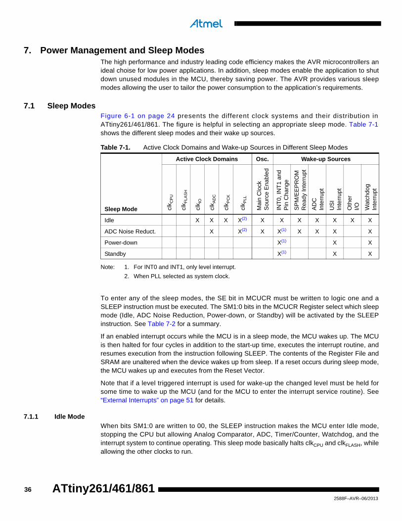
7.1 Sleep ModesFigure 6-1 on page 24 presents the different clock systems and their distribution inATtiny261/461/861. The figure is helpful in selecting an appropriate sleep mode. Table 7-1shows the different sleep modes and their wake up sources.
Note: 1. For INT0 and INT1, only level interrupt.
2. When PLL selected as system clock.
To enter any of the sleep modes, the SE bit in MCUCR must be written to logic one and aSLEEP instruction must be executed. The SM1:0 bits in the MCUCR Register select which sleepmode (Idle, ADC Noise Reduction, Power-down, or Standby) will be activated by the SLEEPinstruction. See Table 7-2 for a summary.
If an enabled interrupt occurs while the MCU is in a sleep mode, the MCU wakes up. The MCUis then halted for four cycles in addition to the start-up time, executes the interrupt routine, andresumes execution from the instruction following SLEEP. The contents of the Register File andSRAM are unaltered when the device wakes up from sleep. If a reset occurs during sleep mode,the MCU wakes up and executes from the Reset Vector.
Note that if a level triggered interrupt is used for wake-up the changed level must be held forsome time to wake up the MCU (and for the MCU to enter the interrupt service routine). See“External Interrupts” on page 51 for details.
7.1.1 Idle Mode
When bits SM1:0 are written to 00, the SLEEP instruction makes the MCU enter Idle mode,stopping the CPU but allowing Analog Comparator, ADC, Timer/Counter, Watchdog, and theinterrupt system to continue operating. This sleep mode basically halts clkCPU and clkFLASH, whileallowing the other clocks to run.
Table 7-1. Active Clock Domains and Wake-up Sources in Different Sleep Modes
Sleep Mode
Active Clock Domains Osc. Wake-up Sources
clk C
PU
clk F
LAS
H
clk I
O
clk A
DC
clk P
CK
clk P
LL
Mai
n C
lock
Sou
rce
Ena
ble
d
INT
0, IN
T1
and
Pin
Cha
nge
SP
M/E
EP
RO
MR
ead
y In
terr
upt
AD
CIn
terr
upt
US
IIn
terr
upt
Oth
erI/O W
atch
dog
Inte
rru
pt
Idle X X X X(2) X X X X X X X
ADC Noise Reduct. X X(2) X X(1) X X X X
Power-down X(1) X X
Standby X(1) X X
362588F–AVR–06/2013
ATtiny261/461/861

ATtiny261/461/861
Idle mode enables the MCU to wake up from external triggered interrupts as well as internalones like the Timer Overflow. If wake-up from the Analog Comparator interrupt is not required,the Analog Comparator can be powered down by setting the ACD bit in the Analog ComparatorControl and Status Register – ACSR. This will reduce power consumption in Idle mode. If theADC is enabled, a conversion starts automatically when this mode is entered.
7.1.2 ADC Noise Reduction Mode
When the SM1:0 bits are written to 01, the SLEEP instruction makes the MCU enter ADC NoiseReduction mode, stopping the CPU but allowing the ADC, the external interrupts, and theWatchdog to continue operating (if enabled). This sleep mode halts clkI/O, clkCPU, and clkFLASH,while allowing the other clocks to run.
This mode improves the noise environment for the ADC, enabling higher resolution measure-ments. If the ADC is enabled, a conversion starts automatically when this mode is entered. Apartform the ADC Conversion Complete interrupt, only an External Reset, a Watchdog Reset, aBrown-out Reset, an SPM/EEPROM ready interrupt, an external level interrupt on INT0 or a pinchange interrupt can wake up the MCU from ADC Noise Reduction mode.
7.1.3 Power-Down Mode
When the SM1:0 bits are written to 10, the SLEEP instruction makes the MCU enter Power-down mode. In this mode, the Oscillator is stopped, while the external interrupts, and the Watch-dog continue operating (if enabled). Only an External Reset, a Watchdog Reset, a Brown-outReset, an external level interrupt on INT0, or a pin change interrupt can wake up the MCU. Thissleep mode halts all generated clocks, allowing operation of asynchronous modules, only.
7.1.4 Standby Mode
When the SM1:0 bits are written to 11 and an external crystal/resonator clock option is selected,the SLEEP instruction makes the MCU enter Standby mode. This mode is identical to Power-down with the exception that the Oscillator is kept running. From Standby mode, the devicewakes up in six clock cycles.
7.2 Power Reduction RegisterThe Power Reduction Register (PRR), see “PRR – Power Reduction Register” on page 39, pro-vides a method to stop the clock to individual peripherals to reduce power consumption. Thecurrent state of the peripheral is frozen and the I/O registers can not be read or written.Resources used by the peripheral when stopping the clock will remain occupied, hence theperipheral should in most cases be disabled before stopping the clock. Waking up a module,which is done by clearing the bit in PRR, puts the module in the same state as before shutdown.
Module shutdown can be used in Idle mode and Active mode to significantly reduce the overallpower consumption. In all other sleep modes, the clock is already stopped. See “Supply Currentof I/O modules” on page 197 for examples. In all other sleep modes, the clock is alreadystopped.
7.3 Minimizing Power ConsumptionThere are several issues to consider when trying to minimize the power consumption in an AVRcontrolled system. In general, sleep modes should be used as much as possible, and the sleepmode should be selected so that as few as possible of the device’s functions are operating. Allfunctions not needed should be disabled. In particular, the following modules may need specialconsideration when trying to achieve the lowest possible power consumption.
372588F–AVR–06/2013

7.3.1 Analog Comparator
When entering Idle mode, the Analog Comparator should be disabled if not used. When enteringADC Noise Reduction mode, the Analog Comparator should be disabled. In the other sleepmodes, the Analog Comparator is automatically disabled. However, if the Analog Comparator isset up to use the Internal Voltage Reference as input, the Analog Comparator should be dis-abled in all sleep modes. Otherwise, the Internal Voltage Reference will be enabled,independent of sleep mode. Refer to “AC – Analog Comparator” on page 137 for details on howto configure the Analog Comparator.
7.3.2 Analog to Digital Converter
If enabled, the ADC will be enabled in all sleep modes. To save power, the ADC should be dis-abled before entering any sleep mode. When the ADC is turned off and on again, the nextconversion will be an extended conversion. Refer to “ADC – Analog to Digital Converter” onpage 142 for details on ADC operation.
7.3.3 Brown-out Detector
If the Brown-out Detector is not needed in the application, this module should be turned off. If theBrown-out Detector is enabled by the BODLEVEL Fuses, it will be enabled in all sleep modes,and hence, always consume power. In the deeper sleep modes, this will contribute significantlyto the total current consumption. Refer to “Brown-out Detection” on page 43 for details on how toconfigure the Brown-out Detector.
7.3.4 Internal Voltage Reference
The Internal Voltage Reference will be enabled when needed by the Brown-out Detection, theAnalog Comparator or the ADC. If these modules are disabled as described in the sectionsabove, the internal voltage reference will be disabled and it will not be consuming power. Whenturned on again, the user must allow the reference to start up before the output is used. If thereference is kept on in sleep mode, the output can be used immediately. Refer to “Internal Volt-age Reference” on page 44 for details on the start-up time.
7.3.5 Watchdog Timer
If the Watchdog Timer is not needed in the application, this module should be turned off. If theWatchdog Timer is enabled, it will be enabled in all sleep modes, and hence, always consumepower. In the deeper sleep modes, this will contribute significantly to the total current consump-tion. Refer to “Watchdog Timer” on page 44 for details on how to configure the Watchdog Timer.
7.3.6 Port Pins
When entering a sleep mode, all port pins should be configured to use minimum power. Themost important thing is then to ensure that no pins drive resistive loads. In sleep modes whereboth the I/O clock (clkI/O) and the ADC clock (clkADC) are stopped, the input buffers of the devicewill be disabled. This ensures that no power is consumed by the input logic when not needed. Insome cases, the input logic is needed for detecting wake-up conditions, and it will then beenabled. Refer to the section “Digital Input Enable and Sleep Modes” on page 59 for details onwhich pins are enabled. If the input buffer is enabled and the input signal is left floating or has ananalog signal level close to VCC/2, the input buffer will use excessive power.
For analog input pins, the digital input buffer should be disabled at all times. An analog signallevel close to VCC/2 on an input pin can cause significant current even in active mode. Digitalinput buffers can be disabled by writing to the Digital Input Disable Registers (DIDR0, DIDR1).
382588F–AVR–06/2013
ATtiny261/461/861

ATtiny261/461/861
Refer to “DIDR0 – Digital Input Disable Register 0” on page 162 or “DIDR1 – Digital Input Dis-able Register 1” on page 162 for details.
7.4 Register Description
7.4.1 MCUCR – MCU Control Register
The MCU Control Register contains control bits for power management.
• Bit 5 – SE: Sleep Enable
The SE bit must be written to logic one to make the MCU enter the sleep mode when the SLEEPinstruction is executed. To avoid the MCU entering the sleep mode unless it is the programmer’spurpose, it is recommended to write the Sleep Enable (SE) bit to one just before the execution ofthe SLEEP instruction and to clear it immediately after waking up.
• Bits 4, 3 – SM1:0: Sleep Mode Select Bits 2:0
These bits select between the three available sleep modes as shown in Table 7-2.
• Bit 2 – Res: Reserved Bit
This bit is reserved and will always read zero.
7.4.2 PRR – Power Reduction Register
The Power Reduction Register provides a method to reduce power consumption by allowingperipheral clock signals to be disabled.
• Bits 7, 6, 5, 4 – Res: Reserved Bits
These bits are reserved and will always read zero.
• Bit 3 – PRTIM1: Power Reduction Timer/Counter1
Writing a logic one to this bit shuts down the Timer/Counter1 module. When the Timer/Counter1is enabled, operation will continue like before the shutdown.
Bit 7 6 5 4 3 2 1 0
0x35 (0x55) – PUD SE SM1 SM0 — ISC01 ISC00 MCUCR
Read/Write R R/W R/W R/W R/W R R/W R/W
Initial Value 0 0 0 0 0 0 0 0
Table 7-2. Sleep Mode Select
SM1 SM0 Sleep Mode
0 0 Idle
0 1 ADC Noise Reduction
1 0 Power-down
1 1 Standby
Bit 7 6 5 4 3 2 1 0
0x36 (0x56) – - - - PRTIM1 PRTIM0 PRUSI PRADC PRR
Read/Write R R R R R/W R/W R/W R/W
Initial Value 0 0 0 0 0 0 0 0
392588F–AVR–06/2013

• Bit 2 – PRTIM0: Power Reduction Timer/Counter0
Writing a logic one to this bit shuts down the Timer/Counter0 module. When the Timer/Counter0is enabled, operation will continue like before the shutdown.
• Bit 1 – PRUSI: Power Reduction USI
Writing a logic one to this bit shuts down the USI by stopping the clock to the module. Whenwaking up the USI again, the USI should be re initialized to ensure proper operation.
• Bit 0 – PRADC: Power Reduction ADC
Writing a logic one to this bit shuts down the ADC. The ADC must be disabled before shut down.Also analog comparator needs this clock.
402588F–AVR–06/2013
ATtiny261/461/861

ATtiny261/461/861
8. System Control and Reset
8.0.1 Resetting the AVR
During reset, all I/O Registers are set to their initial values, and the program starts executionfrom the Reset Vector. The instruction placed at the Reset Vector must be a RJMP – RelativeJump – instruction to the reset handling routine. If the program never enables an interruptsource, the Interrupt Vectors are not used, and regular program code can be placed at theselocations. The circuit diagram in Figure 8-1 shows the reset logic. Electrical parameters of thereset circuitry are given in Table 19-4 on page 190.
Figure 8-1. Reset Logic
The I/O ports of the AVR are immediately reset to their initial state when a reset source goesactive. This does not require any clock source to be running.
After all reset sources have gone inactive, a delay counter is invoked, stretching the internalreset. This allows the power to reach a stable level before normal operation starts. The time-outperiod of the delay counter is defined by the user through the SUT and CKSEL Fuses. The dif-ferent selections for the delay period are presented in “Clock Sources” on page 25.
MCU StatusRegister (MCUSR)
Brown-outReset CircuitBODLEVEL [1..0]
Delay Counters
CKSEL[1:0]
CKTIMEOUT
WD
RF
BO
RF
EX
TR
F
PO
RF
DATA BUS
ClockGenerator
SPIKEFILTER
Pull-up Resistor
WatchdogOscillator
SUT[1:0]
Power-on ResetCircuit
412588F–AVR–06/2013

8.1 Reset SourcesThe ATtiny261/461/861 has four sources of reset:
• Power-on Reset. The MCU is reset when the supply voltage is below the Power-on Reset threshold (VPOT).
• External Reset. The MCU is reset when a low level is present on the RESET pin for longer than the minimum pulse length.
• Watchdog Reset. The MCU is reset when the Watchdog Timer period expires and the Watchdog is enabled.
• Brown-out Reset. The MCU is reset when the supply voltage VCC is below the Brown-out Reset threshold (VBOT) and the Brown-out Detector is enabled.
8.1.1 Power-on Reset
A Power-on Reset (POR) pulse is generated by an On-chip detection circuit. The detection levelis defined in “System and Reset Characteristics” on page 190. The POR is activated wheneverVCC is below the detection level. The POR circuit can be used to trigger the Start-up Reset, aswell as to detect a failure in supply voltage.
A Power-on Reset (POR) circuit ensures that the device is reset from Power-on. Reaching thePower-on Reset threshold voltage invokes the delay counter, which determines how long thedevice is kept in RESET after VCC rise. The RESET signal is activated again, without any delay,when VCC decreases below the detection level.
Figure 8-2. MCU Start-up, RESET Tied to VCC
Figure 8-3. MCU Start-up, RESET Extended Externally
V
RESET
TIME-OUT
INTERNALRESET
tTOUT
VPOT
VRST
CC
RESET
TIME-OUT
INTERNALRESET
tTOUT
VPOT
VRST
VCC
422588F–AVR–06/2013
ATtiny261/461/861
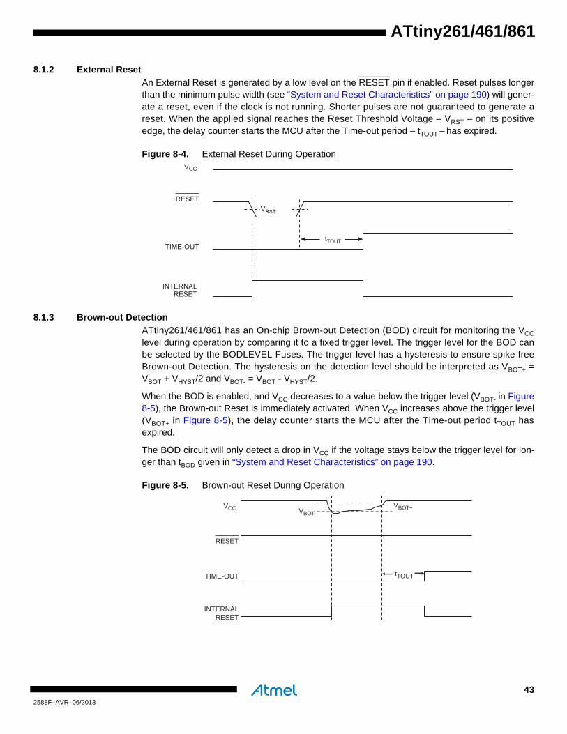
ATtiny261/461/861
8.1.2 External Reset
An External Reset is generated by a low level on the RESET pin if enabled. Reset pulses longerthan the minimum pulse width (see “System and Reset Characteristics” on page 190) will gener-ate a reset, even if the clock is not running. Shorter pulses are not guaranteed to generate areset. When the applied signal reaches the Reset Threshold Voltage – VRST – on its positiveedge, the delay counter starts the MCU after the Time-out period – tTOUT – has expired.
Figure 8-4. External Reset During Operation
8.1.3 Brown-out Detection
ATtiny261/461/861 has an On-chip Brown-out Detection (BOD) circuit for monitoring the VCC
level during operation by comparing it to a fixed trigger level. The trigger level for the BOD canbe selected by the BODLEVEL Fuses. The trigger level has a hysteresis to ensure spike freeBrown-out Detection. The hysteresis on the detection level should be interpreted as VBOT+ =VBOT + VHYST/2 and VBOT- = VBOT - VHYST/2.
When the BOD is enabled, and VCC decreases to a value below the trigger level (VBOT- in Figure8-5), the Brown-out Reset is immediately activated. When VCC increases above the trigger level(VBOT+ in Figure 8-5), the delay counter starts the MCU after the Time-out period tTOUT hasexpired.
The BOD circuit will only detect a drop in VCC if the voltage stays below the trigger level for lon-ger than tBOD given in “System and Reset Characteristics” on page 190.
Figure 8-5. Brown-out Reset During Operation
CC
VCC
RESET
TIME-OUT
INTERNALRESET
VBOT-VBOT+
tTOUT
432588F–AVR–06/2013

8.1.4 Watchdog Reset
When the Watchdog times out, it will generate a short reset pulse of one CK cycle duration. Onthe falling edge of this pulse, the delay timer starts counting the Time-out period tTOUT. Refer to“Watchdog Timer” on page 44 for details on operation of the Watchdog Timer.
Figure 8-6. Watchdog Reset During Operation
8.2 Internal Voltage ReferenceATtiny261/461/861 features an internal bandgap reference. This reference is used for Brown-outDetection, and it can be used as an input to the Analog Comparator or the ADC. The bandgapvoltage varies with supply voltage and temperature, as can be seen in Figure 20-36 on page216.
8.2.1 Voltage Reference Enable Signals and Start-up Time
The voltage reference has a start-up time that may influence the way it should be used. Thestart-up time is given in “System and Reset Characteristics” on page 190. To save power, thereference is not always turned on. The reference is on during the following situations:
1. When the BOD is enabled (by programming the BODLEVEL [2:0] Fuse bits).
2. When the bandgap reference is connected to the Analog Comparator (by setting the ACBG bit in ACSR).
3. When the ADC is enabled.
Thus, when the BOD is not enabled, after setting the ACBG bit or enabling the ADC, the usermust always allow the reference to start up before the output from the Analog Comparator orADC is used. To reduce power consumption in Power-down mode, the user can avoid the threeconditions above to ensure that the reference is turned off before entering Power-down mode.
8.3 Watchdog TimerThe Watchdog Timer is clocked from an on-chip oscillator, which runs at 128 kHz. By controllingthe Watchdog Timer prescaler, the Watchdog Reset interval can be adjusted as shown in Table8-3 on page 49. The WDR – Watchdog Reset – instruction resets the Watchdog Timer. TheWatchdog Timer is also reset when it is disabled and when a device reset occurs. Ten differentclock cycle periods can be selected to determine the reset period. If the reset period expireswithout another Watchdog Reset, the ATtiny261/461/861 resets and executes from the ResetVector. For timing details on the Watchdog Reset, refer to Table 8-3 on page 49.
CK
CC
442588F–AVR–06/2013
ATtiny261/461/861

ATtiny261/461/861
The Wathdog Timer can also be configured to generate an interrupt instead of a reset. This canbe very helpful when using the Watchdog to wake-up from Power-down.
To prevent unintentional disabling of the Watchdog or unintentional change of time-out period,two different safety levels are selected by the fuse WDTON as shown in Table 8-1 Refer to“Timed Sequences for Changing the Configuration of the Watchdog Timer” on page 45 fordetails.
Figure 8-7. Watchdog Timer
8.3.1 Timed Sequences for Changing the Configuration of the Watchdog Timer
The sequence for changing configuration differs slightly between the two safety levels. Separateprocedures are described for each level.
8.3.1.1 Safety Level 1
In this mode, the Watchdog Timer is initially disabled, but can be enabled by writing the WDE bitto one without any restriction. A timed sequence is needed when disabling an enabled Watch-dog Timer. To disable an enabled Watchdog Timer, the following procedure must be followed:
1. In the same operation, write a logic one to WDCE and WDE. A logic one must be writ-ten to WDE regardless of the previous value of the WDE bit.
2. Within the next four clock cycles, in the same operation, write the WDE and WDP bits as desired, but with the WDCE bit cleared.
8.3.1.2 Safety Level 2
In this mode, the Watchdog Timer is always enabled, and the WDE bit will always read as one. Atimed sequence is needed when changing the Watchdog Time-out period. To change theWatchdog Time-out, the following procedure must be followed:
Table 8-1. WDT Configuration as a Function of the Fuse Settings of WDTON
WDTONSafety Level
WDT Initial State
How to Disable the WDT
How to Change Time-out
Unprogrammed 1 Disabled Timed sequence No limitations
Programmed 2 Enabled Always enabled Timed sequence
OS
C/2
K
OS
C/4
K
OS
C/8
K
OS
C/1
6K
OS
C/3
2K
OS
C/6
4K
OS
C/1
28K
OS
C/2
56K
OS
C/5
12K
OS
C/1
024K
MCU RESET
WATCHDOGPRESCALER
128 kHzOSCILLATOR
WATCHDOGRESET
WDP0WDP1WDP2WDP3
WDE
452588F–AVR–06/2013

1. In the same operation, write a logical one to WDCE and WDE. Even though the WDE always is set, the WDE must be written to one to start the timed sequence.
2. Within the next four clock cycles, in the same operation, write the WDP bits as desired, but with the WDCE bit cleared. The value written to the WDE bit is irrelevant.
8.3.2 Code Examples
The following code example shows one assembly and one C function for turning off the WDT.The example assumes that interrupts are controlled (e.g., by disabling interrupts globally) so thatno interrupts will occur during execution of these functions.
Note: See “Code Examples” on page 6.
Assembly Code Example
WDT_off:
wdr
; Clear WDRF in MCUSR
ldi r16, (0<<WDRF)
out MCUSR, r16
; Write logical one to WDCE and WDE
; Keep old prescaler setting to prevent unintentional Watchdog Reset
in r16, WDTCSR
ori r16, (1<<WDCE)|(1<<WDE)
out WDTCSR, r16
; Turn off WDT
ldi r16, (0<<WDE)
out WDTCSR, r16
ret
C Code Example
void WDT_off(void)
{
_WDR();
/* Clear WDRF in MCUSR */
MCUSR = 0x00
/* Write logical one to WDCE and WDE */
WDTCSR |= (1<<WDCE) | (1<<WDE);
/* Turn off WDT */
WDTCSR = 0x00;
}
462588F–AVR–06/2013
ATtiny261/461/861
ATtiny261/461/861
8.4 Register Description
8.4.1 MCUSR – MCU Status Register
The MCU Status Register provides information on which reset source caused an MCU Reset.
• Bits 7:4 – Res: Reserved Bits
These bits are reserved bits in the ATtiny261/461/861 and will always read as zero.
• Bit 3 – WDRF: Watchdog Reset Flag
This bit is set if a Watchdog Reset occurs. The bit is reset by a Power-on Reset, or by writing alogic zero to the flag.
• Bit 2 – BORF: Brown-out Reset Flag
This bit is set if a Brown-out Reset occurs. The bit is reset by a Power-on Reset, or by writing alogic zero to the flag.
• Bit 1 – EXTRF: External Reset Flag
This bit is set if an External Reset occurs. The bit is reset by a Power-on Reset, or by writing alogic zero to the flag.
• Bit 0 – PORF: Power-on Reset Flag
This bit is set if a Power-on Reset occurs. The bit is reset only by writing a logic zero to the flag.
To make use of the Reset Flags to identify a reset condition, the user should read and then resetthe MCUSR as early as possible in the program. If the register is cleared before another resetoccurs, the source of the reset can be found by examining the Reset Flags.
8.4.2 WDTCR – Watchdog Timer Control Register
• Bit 7 – WDIF: Watchdog Timeout Interrupt Flag
This bit is set when a time-out occurs in the Watchdog Timer and the Watchdog Timer is config-ured for interrupt. WDIF is cleared by hardware when executing the corresponding interrupthandling vector. Alternatively, WDIF is cleared by writing a logic one to the flag. When the I-bit inSREG and WDIE are set, the Watchdog Time-out Interrupt is executed.
• Bit 6 – WDIE: Watchdog Timeout Interrupt Enable
When this bit is written to one, WDE is cleared, and the I-bit in the Status Register is set, theWatchdog Time-out Interrupt is enabled. In this mode the corresponding interrupt is executedinstead of a reset if a timeout in the Watchdog Timer occurs.
If WDE is set, WDIE is automatically cleared by hardware when a time-out occurs. This is usefulfor keeping the Watchdog Reset security while using the interrupt. After the WDIE bit is cleared,
Bit 7 6 5 4 3 2 1 0
0x34 (0x54) – – – – WDRF BORF EXTRF PORF MCUSR
Read/Write R R R R R/W R/W R/W R/W
Initial Value 0 0 0 0 See Bit Description
Bit 7 6 5 4 3 2 1 0
0x21 (0x41) WDIF WDIE WDP3 WDCE WDE WDP2 WDP1 WDP0 WDTCR
Read/Write R/W R/W R/W R/W R/W R/W R/W R/W
Initial Value 0 0 0 0 X 0 0 0
472588F–AVR–06/2013

the next time-out will generate a reset. To avoid the Watchdog Reset, WDIE must be set aftereach interrupt.
• Bit 4 – WDCE: Watchdog Change Enable
This bit must be set when the WDE bit is written to logic zero. Otherwise, the Watchdog will notbe disabled. Once written to one, hardware will clear this bit after four clock cycles. Refer to thedescription of the WDE bit for a Watchdog disable procedure. This bit must also be set whenchanging the prescaler bits. See “Timed Sequences for Changing the Configuration of theWatchdog Timer” on page 45.
• Bit 3 – WDE: Watchdog Enable
When the WDE is written to logic one, the Watchdog Timer is enabled, and if the WDE is writtento logic zero, the Watchdog Timer function is disabled. WDE can only be cleared if the WDCE bithas logic level one. To disable an enabled Watchdog Timer, the following procedure must befollowed:
1. In the same operation, write a logic one to WDCE and WDE. A logic one must be writ-ten to WDE even though it is set to one before the disable operation starts.
2. Within the next four clock cycles, write a logic 0 to WDE. This disables the Watchdog.
In safety level 2, it is not possible to disable the Watchdog Timer, even with the algorithmdescribed above. See “Timed Sequences for Changing the Configuration of the WatchdogTimer” on page 45.
In safety level 1, WDE is overridden by WDRF in MCUSR. See “MCUSR – MCU Status Regis-ter” on page 47 for description of WDRF. This means that WDE is always set when WDRF is set.To clear WDE, WDRF must be cleared before disabling the Watchdog with the proceduredescribed above. This feature ensures multiple resets during conditions causing failure, and asafe start-up after the failure.
Note: If the watchdog timer is not going to be used in the application, it is important to go through a watchdog disable procedure in the initialization of the device. If the Watchdog is accidentally enabled, for example by a runaway pointer or brown-out condition, the device will be reset, which in turn will lead to a new watchdog reset. To avoid this situation, the application software should always clear the WDRF flag and the WDE control bit in the initialization routine.
Table 8-2. Watchdog Timer Configuration
WDE WDIE Watchdog Timer State Action on Time-out
0 0 Stopped None
0 1 Running Interrupt
1 0 Running Reset
1 1 Running Interrupt
482588F–AVR–06/2013
ATtiny261/461/861

ATtiny261/461/861
• Bits 5, 2:0 – WDP3:0: Watchdog Timer Prescaler 3, 2, 1, and 0
The WDP3:0 bits determine the Watchdog Timer prescaling when the Watchdog Timer isenabled. The different prescaling values and their corresponding Timeout Periods are shown inTable 8-3.
Notes: 1. If selected, one of the valid settings below 0b1010 will be used.
Table 8-3. Watchdog Timer Prescale Select
WDP3 WDP2 WDP1 WDP0Number of WDT Oscillator
CyclesTypical Time-out at
VCC = 5.0V
0 0 0 0 2K (2048) cycles 16 ms
0 0 0 1 4K (4096) cycles 32 ms
0 0 1 0 8K (8192) cycles 64 ms
0 0 1 1 16K (16384) cycles 0.125 s
0 1 0 0 32K (32764) cycles 0.25 s
0 1 0 1 64K (65536) cycles 0.5 s
0 1 1 0 128K (131072) cycles 1.0 s
0 1 1 1 256K (262144) cycles 2.0 s
1 0 0 0 512K (524288) cycles 4.0 s
1 0 0 1 1024K (1048576) cycles 8.0 s
1 0 1 0
Reserved(1)
1 0 1 1
1 1 0 0
1 1 0 1
1 1 1 0
1 1 1 1
492588F–AVR–06/2013

9. InterruptsThis section describes the specifics of the interrupt handling as performed in ATtiny261/461/861.For a general explanation of the AVR interrupt handling, refer to “Reset and Interrupt Handling”on page 12.
9.1 Interrupt VectorsInterrupt vectors of ATtiny261/461/861 are described in Table 9-1 below.
If the program never enables an interrupt source, the Interrupt Vectors are not used, and regularprogram code can be placed at these locations.
The most typical and general program setup for the Reset and Interrupt Vector Addresses inATtiny261/461/861 is shown in the program example below.
Address Labels Code Comments
0x0000 rjmp RESET ; Reset Handler
0x0001 rjmp EXT_INT0 ; IRQ0 Handler
0x0002 rjmp PCINT ; PCINT Handler
Table 9-1. Reset and Interrupt Vectors
VectorNo.
ProgramAddress Source Interrupt Definition
1 0x0000 RESETExternal Pin, Power-on Reset,Brown-out Reset, Watchdog Reset
2 0x0001 INT0 External Interrupt Request 0
3 0x0002 PCINT Pin Change Interrupt Request
4 0x0003 TIMER1_COMPA Timer/Counter1 Compare Match A
5 0x0004 TIMER1_COMPB Timer/Counter1 Compare Match B
6 0x0005 TIMER1_OVF Timer/Counter1 Overflow
7 0x0006 TIMER0_OVF Timer/Counter0 Overflow
8 0x0007 USI_START USI Start
9 0x0008 USI_OVF USI Overflow
10 0x0009 EE_RDY EEPROM Ready
11 0x000A ANA_COMP Analog Comparator
12 0x000B ADC ADC Conversion Complete
13 0x000C WDT Watchdog Time-out
14 0x000D INT1 External Interrupt Request 1
15 0x000E TIMER0_COMPA Timer/Counter0 Compare Match A
16 0x000F TIMER0_COMPB Timer/Counter0 Compare Match B
17 0x0010 TIMER0_CAPT Timer/Counter1 Capture Event
18 0x0011 TIMER1_COMPD Timer/Counter1 Compare Match D
19 0x0012 FAULT_PROTECTION Timer/Counter1 Fault Protection
502588F–AVR–06/2013
ATtiny261/461/861
ATtiny261/461/861
0x0003 rjmp TIM1_COMPA ; Timer1 CompareA Handler
0x0004 rjmp TIM1_COMPB ; Timer1 CompareB Handler
0x0005 rjmp TIM1_OVF ; Timer1 Overflow Handler
0x0006 rjmp TIM0_OVF ; Timer0 Overflow Handler
0x0007 rjmp USI_START ; USI Start Handler
0x0008 rjmp USI_OVF ; USI Overflow Handler
0x0009 rjmp EE_RDY ; EEPROM Ready Handler
0x000A rjmp ANA_COMP ; Analog Comparator Handler
0x000B rjmp ADC ; ADC Conversion Handler
0x000C rjmp WDT ; WDT Interrupt Handler
0x000D rjmp EXT_INT1 ; IRQ1 Handler
0x000E rjmp TIM0_COMPA ; Timer0 CompareA Handler
0x000F rjmp TIM0_COMPB ; Timer0 CompareB Handler
0x0010 rjmp TIM0_CAPT ; Timer0 Capture Event Handler
0x0011 rjmp TIM1_COMPD ; Timer1 CompareD Handler
0x0012 rjmp FAULT_PROTECTION ; Timer1 Fault Protection
0x0013 RESET: ldi r16, low(RAMEND) ; Main program start
0x0014 ldi r17, high(RAMEND); Tiny861 have also SPH
0x0015 out SPL, r16 ; Set Stack Pointer to top of RAM
0x0016 out SPH, r17 ; Tiny861 have also SPH
0x0017 sei ; Enable interrupts
0x0018 <instr>
... ...
9.2 External InterruptsThe External Interrupts are triggered by the INT0 or INT1 pin or any of the PCINT15:0 pins.Observe that, if enabled, the interrupts will trigger even if the INT0, INT1 or PCINT15:0 pins areconfigured as outputs. This feature provides a way of generating a software interrupt. Pinchange interrupts PCI will trigger if any enabled PCINT15:0 pin toggles. The PCMSK Registercontrol which pins contribute to the pin change interrupts. Pin change interrupts on PCINT15:0are detected asynchronously. This implies that these interrupts can be used for waking the partalso from sleep modes other than Idle mode.
The INT0 and INT1 interrupts can be triggered by a falling or rising edge or a low level. This isset up as indicated in the specification for the MCU Control Register – MCUCR. When the INT0interrupt is enabled and is configured as level triggered, the interrupt will trigger as long as thepin is held low. Note that recognition of falling or rising edge interrupts on INT0 or INT1 requiresthe presence of an I/O clock, described in “Clock Subsystems” on page 24.
9.2.1 Low Level Interrupt
A low level interrupt on INT0 is detected asynchronously. This means that the interrupt sourcecan be used for waking the part also from sleep modes other than Idle (the I/O clock is halted inall sleep modes except Idle).
Note that if a level triggered interrupt is used for wake-up from Power-down, the required levelmust be held long enough for the MCU to complete the wake-up to trigger the level interrupt. Ifthe level disappears before the end of the Start-up Time, the MCU will still wake up, but no inter-
512588F–AVR–06/2013

rupt will be generated. The start-up time is defined by the SUT and CKSEL Fuses as describedin “Clock System” on page 24.
If the low level on the interrupt pin is removed before the device has woken up then programexecution will not be diverted to the interrupt service routine but continue from the instruction fol-lowing the SLEEP command.
9.3 Register Description
9.3.1 MCUCR – MCU Control Register
The MCU Register contains control bits for interrupt sense control.
• Bits 1, 0 – ISC01, ISC00: Interrupt Sense Control 0 Bit 1 and Bit 0
The External Interrupt 0 is activated by the external pin INT0 or INT1 if the SREG I-flag and thecorresponding interrupt mask are set. The level and edges on the external INT0 or INT1 pin thatactivate the interrupt are defined in Table 9-2. The value on the INT0 or INT1 pin is sampledbefore detecting edges. If edge or toggle interrupt is selected, pulses that last longer than oneclock period will generate an interrupt. Shorter pulses are not guaranteed to generate an inter-rupt. If low level interrupt is selected, the low level must be held until the completion of thecurrently executing instruction to generate an interrupt.
9.3.2 GIMSK – General Interrupt Mask Register
• Bit 7 – INT1: External Interrupt Request 1 Enable
When the INT1 bit is set (one) and the I-bit in the Status Register (SREG) is set (one), the exter-nal pin interrupt is enabled. The Interrupt Sense Control0 bits 1/0 (ISC01 and ISC00) in the MCUControl Register (MCUCR) define whether the external interrupt is activated on rising and/or fall-ing edge of the INT1 pin or level sensed. Activity on the pin will cause an interrupt request evenif INT1 is configured as an output. The corresponding interrupt of External Interrupt Request 1 isexecuted from the INT1 Interrupt Vector.
• Bit 6 – INT0: External Interrupt Request 0 Enable
When the INT0 bit is set (one) and the I-bit in the Status Register (SREG) is set (one), the exter-nal pin interrupt is enabled. The Interrupt Sense Control0 bits 1/0 (ISC01 and ISC00) in the MCU
Bit 7 6 5 4 3 2 1 0
0x35 (0x55) – PUD SE SM1 SM0 – ISC01 ISC00 MCUCR
Read/Write R R/W R/W R/W R/W R R/W R/W
Initial Value 0 0 0 0 0 0 0 0
Table 9-2. Interrupt 0 Sense Control
ISC01 ISC00 Description
0 0 The low level of INT0 or INT1 generates an interrupt request.
0 1 Any logical change on INT0 or INT1 generates an interrupt request.
1 0 The falling edge of INT0 or INT1 generates an interrupt request.
1 1 The rising edge of INT0 or INT1 generates an interrupt request.
Bit 7 6 5 4 3 2 1 0
0x3B (0x5B) INT1 INT0 PCIE1 PCIE0 – – – – GIMSK
Read/Write R/W R/W R/W R/w R R R R
Initial Value 0 0 0 0 0 0 0 0
522588F–AVR–06/2013
ATtiny261/461/861

ATtiny261/461/861
Control Register (MCUCR) define whether the external interrupt is activated on rising and/or fall-ing edge of the INT0 pin or level sensed. Activity on the pin will cause an interrupt request evenif INT0 is configured as an output. The corresponding interrupt of External Interrupt Request 0 isexecuted from the INT0 Interrupt Vector.
• Bit 5 – PCIE1: Pin Change Interrupt Enable
When the PCIE1 bit is set (one) and the I-bit in the Status Register (SREG) is set (one), pinchange interrupt is enabled. Any change on any enabled PCINT7:0 or PCINT15:12 pin willcause an interrupt. The corresponding interrupt of Pin Change Interrupt Request is executedfrom the PCI Interrupt Vector. PCINT7:0 and PCINT15:12 pins are enabled individually by thePCMSK0 and PCMSK1 Register.
• Bit 4 – PCIE0: Pin Change Interrupt Enable
When the PCIE0 bit is set (one) and the I-bit in the Status Register (SREG) is set (one), pinchange interrupt is enabled. Any change on any enabled PCINT11:8 pin will cause an interrupt.The corresponding interrupt of Pin Change Interrupt Request is executed from the PCI InterruptVector. PCINT11:8 pins are enabled individually by the PCMSK1 Register.
• Bits 3:0 – Res: Reserved Bits
These bits are reserved and will always read as zero.
9.3.3 GIFR – General Interrupt Flag Register
• Bit 7 – INTF1: External Interrupt Flag 1
When an edge or logic change on the INT1 pin triggers an interrupt request, INTF1 becomes set(one). If the I-bit in SREG and the INT1 bit in GIMSK are set (one), the MCU will jump to the cor-responding Interrupt Vector. The flag is cleared when the interrupt routine is executed.Alternatively, the flag can be cleared by writing a logical one to it. This flag is always clearedwhen INT1 is configured as a level interrupt.
• Bit 6 – INTF0: External Interrupt Flag 0
When an edge or logic change on the INT0 pin triggers an interrupt request, INTF0 becomes set(one). If the I-bit in SREG and the INT0 bit in GIMSK are set (one), the MCU will jump to the cor-responding Interrupt Vector. The flag is cleared when the interrupt routine is executed.Alternatively, the flag can be cleared by writing a logical one to it. This flag is always clearedwhen INT0 is configured as a level interrupt.
• Bit 5 – PCIF: Pin Change Interrupt Flag
When a logic change on any PCINT15 pin triggers an interrupt request, PCIF becomes set(one). If the I-bit in SREG and the PCIE bit in GIMSK are set (one), the MCU will jump to the cor-responding Interrupt Vector. The flag is cleared when the interrupt routine is executed.Alternatively, the flag can be cleared by writing a logical one to it.
• Bits 4:0 – Res: Reserved Bits
These bits are reserved and will always read as zero.
Bit 7 6 5 4 3 2 1 0
0x3A (0x5A) INT1 INTF0 PCIF – – – – – GIFR
Read/Write R/W R/W R/W R R R R R
Initial Value 0 0 0 0 0 0 0 0
532588F–AVR–06/2013

9.3.4 PCMSK0 – Pin Change Mask Register A
• Bits 7:0 – PCINT7:0: Pin Change Enable Mask 7:0
Each PCINT7:0 bit selects whether pin change interrupt is enabled on the corresponding I/O pin.If PCINT7:0 is set and the PCIE1 bit in GIMSK is set, pin change interrupt is enabled on the cor-responding I/O pin. If PCINT7:0 is cleared, pin change interrupt on the corresponding I/O pin isdisabled.
9.3.5 PCMSK1 – Pin Change Mask Register B
• Bits 7:0 – PCINT15:8: Pin Change Enable Mask 15:8
Each PCINT15:8 bit selects whether pin change interrupt is enabled on the corresponding I/Opin. If PCINT11:8 is set and the PCIE0 bit in GIMSK is set, pin change interrupt is enabled onthe corresponding I/O pin, and if PCINT15:12 is set and the PCIE1 bit in GIMSK is set, pinchange interrupt is enabled on the corresponding I/O pin. If PCINT15:8 is cleared, pin changeinterrupt on the corresponding I/O pin is disabled.
Bit 7 6 5 4 3 2 1 0
0x23 (0x43) PCINT7 PCINT6 PCINT5 PCINT4 PCINT3 PCINT2 PCINT1 PCINT0 PCMSK0
Read/Write R/W R/W R/W R/w R/W R/W R/W R/W
Initial Value 1 1 0 0 1 0 0 0
Bit 7 6 5 4 3 2 1 0
0x22 (0x42) PCINT15 PCINT14 PCINT13 PCINT12 PCINT11 PCINT10 PCINT9 PCINT8 PCMSK1
Read/Write R/W R/W R/W R/w R/W R/W R/W R/W
Initial Value 1 1 1 1 1 1 1 1
542588F–AVR–06/2013
ATtiny261/461/861

ATtiny261/461/861
10. I/O PortsAll AVR ports have true Read-Modify-Write functionality when used as general digital I/O ports.This means that the direction of one port pin can be changed without unintentionally changingthe direction of any other pin with the SBI and CBI instructions. The same applies when chang-ing drive value (if configured as output) or enabling/disabling of pull-up resistors (if configured asinput). Each output buffer has symmetrical drive characteristics with both high sink and sourcecapability. The pin driver is strong enough to drive LED displays directly. All port pins have indi-vidually selectable pull-up resistors with a supply-voltage invariant resistance. All I/O pins haveprotection diodes to both VCC and Ground as indicated in Figure 10-1. See “Electrical Character-istics” on page 187 for a complete list of parameters.
Figure 10-1. I/O Pin Equivalent Schematic
All registers and bit references in this section are written in general form. A lower case “x” repre-sents the numbering letter for the port, and a lower case “n” represents the bit number. However,when using the register or bit defines in a program, the precise form must be used. For example,PORTB3 for bit no. 3 in Port B, here documented generally as PORTxn. The physical I/O Regis-ters and bit locations are listed in “Register Description” on page 69.
Three I/O memory address locations are allocated for each port, one each for the Data Register– PORTx, Data Direction Register – DDRx, and the Port Input Pins – PINx. The Port Input PinsI/O location is read only, while the Data Register and the Data Direction Register are read/write.However, writing a logic one to a bit in the PINx Register, will result in a toggle in the correspond-ing bit in the Data Register. In addition, the Pull-up Disable – PUD bit in MCUCR disables thepull-up function for all pins in all ports when set.
Using the I/O port as General Digital I/O is described in “Ports as General Digital I/O” on page56. Most port pins are multiplexed with alternate functions for the peripheral features on thedevice. How each alternate function interferes with the port pin is described in “Alternate PortFunctions” on page 60. Refer to the individual module sections for a full description of the alter-nate functions.
Note that enabling the alternate function of some of the port pins does not affect the use of theother pins in the port as general digital I/O.
CPIN
Logic
RPU
See Figure"General Digital I/O" for
Details
Pxn
552588F–AVR–06/2013

10.1 Ports as General Digital I/OThe ports are bi-directional I/O ports with optional internal pull-ups. Figure 10-2 shows a func-tional description of one I/O-port pin, here generically called Pxn.
Figure 10-2. General Digital I/O(1)
Note: 1. WRx, WPx, WDx, RRx, RPx, and RDx are common to all pins within the same port. clkI/O, SLEEP, and PUD are common to all ports.
10.1.1 Configuring the Pin
Each port pin consists of three register bits: DDxn, PORTxn, and PINxn. As shown in “RegisterDescription” on page 69, the DDxn bits are accessed at the DDRx I/O address, the PORTxn bitsat the PORTx I/O address, and the PINxn bits at the PINx I/O address.
The DDxn bit in the DDRx Register selects the direction of this pin. If DDxn is written logic one,Pxn is configured as an output pin. If DDxn is written logic zero, Pxn is configured as an inputpin.
If PORTxn is written logic one when the pin is configured as an input pin, the pull-up resistor isactivated. To switch the pull-up resistor off, PORTxn has to be written logic zero or the pin has to
clk
RPx
RRx
RDx
WDx
PUD
SYNCHRONIZER
WDx: WRITE DDRx
WRx: WRITE PORTxRRx: READ PORTx REGISTERRPx: READ PORTx PIN
PUD: PULLUP DISABLE
clkI/O: I/O CLOCK
RDx: READ DDRx
D
L
Q
Q
RESET
RESET
Q
QD
Q
Q D
CLR
PORTxn
Q
Q D
CLR
DDxn
PINxn
DAT
A B
US
SLEEP
SLEEP: SLEEP CONTROL
Pxn
I/O
WPx
0
1
WRx
WPx: WRITE PINx REGISTER
562588F–AVR–06/2013
ATtiny261/461/861

ATtiny261/461/861
be configured as an output pin. The port pins are tri-stated when reset condition becomes active,even if no clocks are running.
If PORTxn is written logic one when the pin is configured as an output pin, the port pin is drivenhigh (one). If PORTxn is written logic zero when the pin is configured as an output pin, the portpin is driven low (zero).
The pull-up resistor is activated, if the PUExn is written logic one. To switch the pull-up resistoroff, PUExn has to be written logic zero.
10.1.2 Toggling the Pin
Writing a logic one to PINxn toggles the value of PORTxn, independent on the value of DDRxn.Note that the SBI instruction can be used to toggle one single bit in a port.
10.1.3 Switching Between Input and Output
When switching between tri-state ({DDxn, PORTxn} = 0b00) and output high ({DDxn, PORTxn}= 0b11), an intermediate state with either pull-up enabled {DDxn, PORTxn} = 0b01) or outputlow ({DDxn, PORTxn} = 0b10) must occur. Normally, the pull-up enabled state is fully accept-able, as a high-impedant environment will not notice the difference between a strong high driverand a pull-up. If this is not the case, the PUD bit in the MCUCR Register can be set to disable allpull-ups in all ports.
Switching between input with pull-up and output low generates the same problem. The usermust use either the tri-state ({DDxn, PORTxn} = 0b00) or the output high state ({DDxn, PORTxn}= 0b10) as an intermediate step.
Table 10-1 summarizes the control signals for the pin value.
10.1.4 Reading the Pin Value
Independent of the setting of Data Direction bit DDxn, the port pin can be read through thePINxn Register bit. As shown in Figure 10-2, the PINxn Register bit and the preceding latch con-stitute a synchronizer. This is needed to avoid metastability if the physical pin changes valuenear the edge of the internal clock, but it also introduces a delay. Figure 10-3 shows a timing dia-gram of the synchronization when reading an externally applied pin value. The maximum andminimum propagation delays are denoted tpd,max and tpd,min respectively.
Table 10-1. Port Pin Configurations
DDxn PORTxnPUD
(in MCUCR) I/O Pull-up Comment
0 0 X Input No Tri-state (Hi-Z)
0 1 0 Input Yes Pxn will source current if ext. pulled low
0 1 1 Input No Tri-state (Hi-Z)
1 0 X Output No Output Low (Sink)
1 1 X Output No Output High (Source)
572588F–AVR–06/2013

Figure 10-3. Synchronization when Reading an Externally Applied Pin value
Consider the clock period starting shortly after the first falling edge of the system clock. The latchis closed when the clock is low, and goes transparent when the clock is high, as indicated by theshaded region of the “SYNC LATCH” signal. The signal value is latched when the system clockgoes low. It is clocked into the PINxn Register at the succeeding positive clock edge. As indi-cated by the two arrows tpd,max and tpd,min, a single signal transition on the pin will be delayedbetween ½ and 1½ system clock period depending upon the time of assertion.
When reading back a software assigned pin value, a nop instruction must be inserted as indi-cated in Figure 10-4. The out instruction sets the “SYNC LATCH” signal at the positive edge ofthe clock. In this case, the delay tpd through the synchronizer is one system clock period.
Figure 10-4. Synchronization when Reading a Software Assigned Pin Value
XXX in r17, PINx
0x00 0xFF
INSTRUCTIONS
SYNC LATCH
PINxn
r17
XXX
SYSTEM CLK
tpd, max
tpd, min
out PORTx, r16 nop in r17, PINx
0xFF
0x00 0xFF
SYSTEM CLK
r16
INSTRUCTIONS
SYNC LATCH
PINxn
r17
tpd
582588F–AVR–06/2013
ATtiny261/461/861

ATtiny261/461/861
10.1.5 Digital Input Enable and Sleep Modes
As shown in Figure 10-2, the digital input signal can be clamped to ground at the input of theschmitt-trigger. The signal denoted SLEEP in the figure, is set by the MCU Sleep Controller inPower-down mode, Power-save mode, and Standby mode to avoid high power consumption ifsome input signals are left floating, or have an analog signal level close to VCC/2.
SLEEP is overridden for port pins enabled as external interrupt pins. If the external interruptrequest is not enabled, SLEEP is active also for these pins. SLEEP is also overridden by variousother alternate functions as described in “Alternate Port Functions” on page 60.
If a logic high level (“one”) is present on an asynchronous external interrupt pin configured as“Interrupt on Rising Edge, Falling Edge, or Any Logic Change on Pin” while the external interruptis not enabled, the corresponding External Interrupt Flag will be set when resuming from theabove mentioned Sleep mode, as the clamping in these sleep mode produces the requestedlogic change.
10.1.6 Unconnected Pins
If some pins are unused, it is recommended to ensure that these pins have a defined level. Eventhough most of the digital inputs are disabled in the deep sleep modes as described above, float-ing inputs should be avoided to reduce current consumption in all other modes where the digitalinputs are enabled (Reset, Active mode and Idle mode).
The simplest method to ensure a defined level of an unused pin, is to enable the internal pull-up.In this case, the pull-up will be disabled during reset. If low power consumption during reset isimportant, it is recommended to use an external pull-up or pulldown. Connecting unused pinsdirectly to VCC or GND is not recommended, since this may cause excessive currents if the pin isaccidentally configured as an output.
10.1.7 Program Examples
The following code examples show how to set port B pins 0 and 1 high, 2 and 3 low, and definethe port pins from 4 to 5 as input with a pull-up assigned to port pin 4. The resulting pin valuesare read back again, but as previously discussed, a nop instruction is included to be able to readback the value recently assigned to some of the pins.
Note: Two temporary registers are used to minimize the time from pull-ups are set on pins 0, 1 and 4, until the direction bits are correctly set, defining bit 2 and 3 as low and redefining bits 0 and 1 as strong high drivers.
Assembly Code Example
...
; Define pull-ups and set outputs high
; Define directions for port pins
ldi r16,(1<<PB4)|(1<<PB1)|(1<<PB0)
ldi r17,(1<<DDB3)|(1<<DDB2)|(1<<DDB1)|(1<<DDB0)
out PORTB,r16
out DDRB,r17
; Insert nop for synchronization
nop
; Read port pins
in r16,PINB
...
592588F–AVR–06/2013

Note: See “Code Examples” on page 6.
10.2 Alternate Port FunctionsMost port pins have alternate functions in addition to being general digital I/Os. Figure 10-5shows how the port pin control signals from the simplified Figure 10-2 can be overridden byalternate functions. The overriding signals may not be present in all port pins, but the figureserves as a generic description applicable to all port pins in the AVR microcontroller family.
C Code Example
unsigned char i;
...
/* Define pull-ups and set outputs high */
/* Define directions for port pins */
PORTB = (1<<PB4)|(1<<PB1)|(1<<PB0);
DDRB = (1<<DDB3)|(1<<DDB2)|(1<<DDB1)|(1<<DDB0);
/* Insert nop for synchronization*/
_NOP();
/* Read port pins */
i = PINB;
...
602588F–AVR–06/2013
ATtiny261/461/861

ATtiny261/461/861
Figure 10-5. Alternate Port Functions(1)
Note: 1. WRx, WPx, WDx, RRx, RPx, and RDx are common to all pins within the same port. clkI/O, SLEEP, and PUD are common to all ports. All other signals are unique for each pin.
clk
RPx
RRxWRx
RDx
WDx
PUD
SYNCHRONIZER
WDx: WRITE DDRx
WRx: WRITE PORTxRRx: READ PORTx REGISTER
RPx: READ PORTx PIN
PUD: PULLUP DISABLE
clkI/O: I/O CLOCK
RDx: READ DDRx
D
L
Q
Q
SET
CLR
0
1
0
1
0
1
DIxn
AIOxn
DIEOExn
PVOVxn
PVOExn
DDOVxn
DDOExn
PUOExn
PUOVxn
PUOExn: Pxn PULL-UP OVERRIDE ENABLEPUOVxn: Pxn PULL-UP OVERRIDE VALUEDDOExn: Pxn DATA DIRECTION OVERRIDE ENABLEDDOVxn: Pxn DATA DIRECTION OVERRIDE VALUEPVOExn: Pxn PORT VALUE OVERRIDE ENABLEPVOVxn: Pxn PORT VALUE OVERRIDE VALUE
DIxn: DIGITAL INPUT PIN n ON PORTxAIOxn: ANALOG INPUT/OUTPUT PIN n ON PORTx
RESET
RESET
Q
Q D
CLR
Q
Q D
CLR
Q
QD
CLR
PINxn
PORTxn
DDxn
DAT
A B
US
0
1DIEOVxn
SLEEP
DIEOExn: Pxn DIGITAL INPUT-ENABLE OVERRIDE ENABLEDIEOVxn: Pxn DIGITAL INPUT-ENABLE OVERRIDE VALUESLEEP: SLEEP CONTROL
Pxn
I/O
0
1
PTOExn
PTOExn: Pxn, PORT TOGGLE OVERRIDE ENABLE
WPx: WRITE PINx
WPx
612588F–AVR–06/2013

Table 10-2 summarizes the function of the overriding signals. The pin and port indexes from Fig-ure 10-5 are not shown in the succeeding tables. The overriding signals are generated internallyin the modules having the alternate function.
The following subsections shortly describe the alternate functions for each port, and relate theoverriding signals to the alternate function. Refer to the alternate function description for furtherdetails.
Table 10-2. Generic Description of Overriding Signals for Alternate Functions
Signal Name Full Name Description
PUOEPull-up Override Enable
If this signal is set, the pull-up enable is controlled by the PUOV signal. If this signal is cleared, the pull-up is enabled when {DDxn, PORTxn, PUD} = 0b010.
PUOVPull-up Override Value
If PUOE is set, the pull-up is enabled/disabled when PUOV is set/cleared, regardless of the setting of the DDxn, PORTxn, and PUD Register bits.
DDOEData Direction Override Enable
If this signal is set, the Output Driver Enable is controlled by the DDOV signal. If this signal is cleared, the Output driver is enabled by the DDxn Register bit.
DDOVData Direction Override Value
If DDOE is set, the Output Driver is enabled/disabled when DDOV is set/cleared, regardless of the setting of the DDxn Register bit.
PVOEPort Value Override Enable
If this signal is set and the Output Driver is enabled, the port value is controlled by the PVOV signal. If PVOE is cleared, and the Output Driver is enabled, the port Value is controlled by the PORTxn Register bit.
PVOVPort Value Override Value
If PVOE is set, the port value is set to PVOV, regardless of the setting of the PORTxn Register bit.
PTOEPort Toggle Override Enable
If PTOE is set, the PORTxn Register bit is inverted.
DIEOEDigital Input Enable Override Enable
If this bit is set, the Digital Input Enable is controlled by the DIEOV signal. If this signal is cleared, the Digital Input Enable is determined by MCU state (Normal mode, sleep mode).
DIEOVDigital Input Enable Override Value
If DIEOE is set, the Digital Input is enabled/disabled when DIEOV is set/cleared, regardless of the MCU state (Normal mode, sleep mode).
DI Digital Input
This is the Digital Input to alternate functions. In the figure, the signal is connected to the output of the schmitt-trigger but before the synchronizer. Unless the Digital Input is used as a clock source, the module with the alternate function will use its own synchronizer.
AIOAnalog Input/Output
This is the Analog Input/Output to/from alternate functions. The signal is connected directly to the pad, and can be used bi-directionally.
622588F–AVR–06/2013
ATtiny261/461/861

ATtiny261/461/861
10.2.1 Alternate Functions of Port A
The Port A pins with alternate function are shown in Table 10-3.
• Port A, Bit 7 – ADC6/AIN0/PCINT7
• ADC6: Analog to Digital Converter, Channel 6.
• AIN0: Analog Comparator Input. Configure the port pin as input with the internal pull-up switched off to avoid the digital port function from interfering with the function of the Analog Comparator.
• PCINT7: Pin Change Interrupt source 8.
• Port A, Bit 6 – ADC5/AIN1/PCINT6
• ADC5: Analog to Digital Converter, Channel 5.
• AIN1: Analog Comparator Input. Configure the port pin as input with the internal pull-up switched off to avoid the digital port function from interfering with the function of the Analog Comparator.
• PCINT6: Pin Change Interrupt source 6.
Table 10-3. Port B Pins Alternate Functions
Port Pin Alternate Function
PA7
ADC6: ADC Input Channel 6
AIN0: Analog Comparator Input
PCINT7: Pin Change Interrupt 0, Source 7
PA6
ADC5: ADC Input Channel 5
AIN1: Analog Comparator Input
PCINT6: Pin Change Interrupt 0, Source 6
PA5
ADC4: ADC Input Channel 4
AIN2: Analog Comparator Input
PCINT5: Pin Change Interrupt 0, Source 5
PA4
ADC3: ADC Input Channel 3
ICP0: Timer/Counter0 Input Capture Pin
PCINT4: Pin Change Interrupt 0, Source 4
PA3AREF: External Analog Reference
PCINT3: Pin Change Interrupt 0, Source 3
PA2
ADC2: ADC Input Channel 2
INT1: External Interrupt 1 Input
USCK: USI Clock (Three Wire Mode)SCL : USI Clock (Two Wire Mode)
PCINT2: Pin Change Interrupt 0, Source 2
PA1
ADC1: ADC Input Channel 1
DO: USI Data Output (Three Wire Mode)
PCINT1:Pin Change Interrupt 0, Source 1
PA0
ADC0: ADC Input Channel 0
DI: USI Data Input (Three Wire Mode)
SDA: USI Data Input (Two Wire Mode)
PCINT0: Pin Change Interrupt 0, Source 0
632588F–AVR–06/2013

• Port A, Bit 5 – ADC4/AIN2/PCINT5
• ADC4: Analog to Digital Converter, Channel 4.
• AIN2: Analog Comparator Input. Configure the port pin as input with the internal pull-up switched off to avoid the digital port function from interfering with the function of the Analog Comparator.
• PCINT5: Pin Change Interrupt source 5.
• Port A, Bit 4 – ADC3/ICP0/PCINT4
• ADC3: Analog to Digital Converter, Channel 3.
• ICP0: Timer/Counter0 Input Capture Pin.
• PCINT4: Pin Change Interrupt source 4.
• Port A, Bit 3 – AREF/PCINT3
• AREF: External analog reference for ADC. Pullup and output driver are disabled on PA3 when the pin is used as an external reference or internal voltage reference with external capacitor at the AREF pin.
• PCINT3: Pin Change Interrupt source 3.
• Port A, Bit 2 – ADC2/INT1/USCK/SCL/PCINT2
• ADC2: Analog to Digital Converter, Channel 2.
• INT1: The PA2 pin can serve as an External Interrupt source 1.
• USCK: Three-wire mode Universal Serial Interface Clock.
• SCL: Two-wire mode Serial Clock for USI Two-wire mode.
• PCINT2: Pin Change Interrupt source 2.
• Port A, Bit 1 – ADC1/DO/PCINT1
• ADC1: Analog to Digital Converter, Channel 1.
• DO: Three-wire mode Universal Serial Interface Data output. Three-wire mode Data output overrides PORTA1 value and it is driven to the port when data direction bit DDA1 is set. PORTA1 still enables the pull-up, if the direction is input and PORTA1 is set.
• PCINT1: Pin Change Interrupt source 1.
• Port A, Bit 0 – ADC0/DI/SDA/PCINT0
• ADC0: Analog to Digital Converter, Channel 0.
• DI: Data Input in USI Three-wire mode. USI Three-wire mode does not override normal port functions, so pin must be configure as an input for DI function.
• SDA: Two-wire mode Serial Interface Data.
• PCINT0: Pin Change Interrupt source 0.
642588F–AVR–06/2013
ATtiny261/461/861

ATtiny261/461/861
Table 10-4 and Table 10-5 relate the alternate functions of Port A to the overriding signalsshown in Figure 10-5 on page 61.
Table 10-4. Overriding Signals for Alternate Functions in PA7:PA4
Signal Name
PA7/ADC6/AIN0/
PCINT7
PA6/ADC5/AIN1/
PCINT6
PA5/ADC4/AIN2/
PCINT5
PA4/ADC3/ICP0/
PCINT4
PUOE 0 0 0 0
PUOV 0 0 0 0
DDOE 0 0 0 0
DDOV 0 0 0 0
PVOE 0 0 0 0
PVOV 0 0 0 0
PTOE 0 0 0 0
DIEOE PCINT7 • PCIE + ADC6D
PCINT6 • PCIE + ADC5D
PCINT5 • PCIE + ADC4D
PCINT4 • PCIE + ADC3D
DIEOV ADC6D ADC5D ADC4D ADC3D
DI PCINT7 PCINT6 PCINT5 ICP0/PCINT4
AIO ADC6, AIN0 ADC5, AIN1 ADC4, AIN2 ADC3
Table 10-5. Overriding Signals for Alternate Functions in PA3:PA0
Signal Name
PA3/AREF/
PCINT3
PA2/ADC2/INT1/
USCK/SCL/PCINT2
PA1/ADC1/DO/
PCINT1
PA0/ADC0/DI/SDA/
PCINT0
PUOE 0 0 0 0
PUOV 0 0 0 0
DDOE 0 USI_TWO_WIRE • USIPOS
0USI_TWO_WIRE • USIPOS
DDOV 0 (USI_SCL_HOLD + PORTB2) • DDB2 • USIPOS
0(SDA + PORTB0) • DDRB0 • USIPOS
PVOE 0 USI_TWO_WIRE • DDRB2
USI_THREE_WIRE • USIPOS
USI_TWO_WIRE • DDRB0 • USIPOS
PVOV 0 0 DO • USIPOS 0
PTOE 0 USI_PTOE • USIPOS 0 0
DIEOE PCINT3 • PCIE
PCINT2 • PCIE + INT1 + ADC2D + USISIE • USIPOS
PCINT1 • PCIE + ADC1D
PCINT0 • PCIE + ADC0D + USISIE • USIPOS
DIEOV 0 ADC2D ADC1D ADC0D
DI PCINT3 USCK/SCL/INT1/ PCINT2 PCINT1 DI/SDA/PCINT0
AIO AREF ADC2 ADC1 ADC0
652588F–AVR–06/2013

10.2.2 Alternate Functions of Port B
The Port B pins with alternate function are shown in Table 10-6.
• Port B, Bit 7 – RESET/ dW/ ADC10/ PCINT15
• RESET, Reset pin: When the RSTDISBL Fuse is programmed, this pin functions as a normal I/O pin, and the part will have to rely on Power-on Reset and Brown-out Reset as its reset sources. When the RSTDISBL Fuse is unprogrammed, the reset circuitry is connected to the pin, and the pin can not be used as an I/O pin.
• If PB7 is used as a reset pin, DDB7, PORTB7 and PINB7 will all read 0.
• dW: When the debugWIRE Enable (DWEN) Fuse is programmed and Lock bits are unprogrammed, the RESET port pin is configured as a wire-AND (open-drain) bi-directional I/O pin with pull-up enabled and becomes the communication gateway between target and emulator.
Table 10-6. Port B Pins Alternate Functions
Port Pin Alternate Function
PB7
RESET: Reset pin
dW: debugWire I/O
ADC10: ADC Input Channel 10
PCINT15:Pin Change Interrupt 0, Source 15
PB6
ADC9: ADC Input Channel 9
T0: Timer/Counter0 Clock Source
INT0: External Interrupt 0 Input
PCINT14:Pin Change Interrupt 0, Source 14
PB5
XTAL2: Crystal Oscillator Output
CLKO: System Clock Output
OC1D: Timer/Counter1 Compare Match D Output
ADC8: ADC Input Channel 8
PCINT13:Pin Change Interrupt 0, Source 13
PB4
XTAL1: Crystal Oscillator Input
CLKI: External Clock Input
OC1D: Inverted Timer/Counter1 Compare Match D Output
ADC7: ADC Input Channel 7
PCINT12:Pin Change Interrupt 0, Source 12
PB3OC1B: Timer/Counter1 Compare Match B Output
PCINT11:Pin Change Interrupt 0, Source 11
PB2
USCK: USI Clock (Three Wire Mode)SCL : USI Clock (Two Wire Mode)
OC1B: Inverted Timer/Counter1 Compare Match B Output
PCINT10:Pin Change Interrupt 0, Source 10
PB1
DO: USI Data Output (Three Wire Mode)
OC1A: Timer/Counter1 Compare Match A Output
PCINT9: Pin Change Interrupt 1, Source 9
PB0
DI: USI Data Input (Three Wire Mode)
SDA: USI Data Input (Two Wire Mode)
OC1A: Inverted Timer/Counter1 Compare Match A Output
PCINT8: Pin Change Interrupt 1, Source 8
662588F–AVR–06/2013
ATtiny261/461/861

ATtiny261/461/861
• ADC10: ADC input Channel 10. Note that ADC input channel 10 uses analog power.
• PCINT15: Pin Change Interrupt source 15.
• Port B, Bit 6 – ADC9/ T0/ INT0/ PCINT14
• ADC9: ADC input Channel 9. Note that ADC input channel 9 uses analog power.
• T0: Timer/Counter0 counter source.
• INT0: The PB6 pin can serve as an External Interrupt source 0.
• PCINT14: Pin Change Interrupt source 14.
• Port B, Bit 5 – XTAL2/ CLKO/ ADC8/ PCINT13
• XTAL2: Chip clock Oscillator pin 2. Used as clock pin for crystal Oscillator or Low-frequency crystal Oscillator. When used as a clock pin, the pin can not be used as an I/O pin.
• CLKO: The divided system clock can be output on the PB5 pin, if the CKOUT Fuse is programmed, regardless of the PORTB5 and DDB5 settings. It will also be output during reset.
• OC1D Output Compare Match output: The PB5 pin can serve as an external output for the Timer/Counter1 Compare Match D when configured as an output (DDA1 set). The OC1D pin is also the output pin for the PWM mode timer function.
• ADC8: ADC input Channel 8. Note that ADC input channel 8 uses analog power.
• PCINT13: Pin Change Interrupt source 13.
• Port B, Bit 4 – XTAL1/ CLKI/ OC1B/ ADC7/ PCINT12
• XTAL1/CLKI: Chip clock Oscillator pin 1. Used for all chip clock sources except internal calibrated RC Oscillator. When used as a clock pin, the pin can not be used as an I/O pin.
• OC1D: Inverted Output Compare Match output: The PB4 pin can serve as an external output for the Timer/Counter1 Compare Match D when configured as an output (DDA0 set). The OC1D pin is also the inverted output pin for the PWM mode timer function.
• ADC7: ADC input Channel 7. Note that ADC input channel 7 uses analog power.
• PCINT12: Pin Change Interrupt source 12.
• Port B, Bit 3 – OC1B/ PCINT11
• OC1B, Output Compare Match output: The PB3 pin can serve as an external output for the Timer/Counter1 Compare Match B. The PB3 pin has to be configured as an output (DDB3 set (one)) to serve this function. The OC1B pin is also the output pin for the PWM mode timer function.
• PCINT11: Pin Change Interrupt source 11.
• Port B, Bit 2 – SCK/ USCK/ SCL/ OC1B/ PCINT10
• USCK: Three-wire mode Universal Serial Interface Clock.
• SCL: Two-wire mode Serial Clock for USI Two-wire mode.
• OC1B: Inverted Output Compare Match output: The PB2 pin can serve as an external output for the Timer/Counter1 Compare Match B when configured as an output (DDB2 set). The OC1B pin is also the inverted output pin for the PWM mode timer function.
• PCINT10: Pin Change Interrupt source 10.
672588F–AVR–06/2013

• Port B, Bit 1 – MISO/ DO/ OC1A/ PCINT9
• DO: Three-wire mode Universal Serial Interface Data output. Three-wire mode Data output overrides PORTB1 value and it is driven to the port when data direction bit DDB1 is set (one). PORTB1 still enables the pull-up, if the direction is input and PORTB1 is set (one).
• OC1A: Output Compare Match output: The PB1 pin can serve as an external output for the Timer/Counter1 Compare Match B when configured as an output (DDB1 set). The OC1A pin is also the output pin for the PWM mode timer function.
• PCINT9: Pin Change Interrupt source 9.
• Port B, Bit 0 – MOSI/ DI/ SDA/ OC1A/ PCINT8
• DI: Data Input in USI Three-wire mode. USI Three-wire mode does not override normal port functions, so pin must be configure as an input for DI function.
• SDA: Two-wire mode Serial Interface Data.
• OC1A: Inverted Output Compare Match output: The PB0 pin can serve as an external output for the Timer/Counter1 Compare Match B when configured as an output (DDB0 set). The OC1A pin is also the inverted output pin for the PWM mode timer function.
• PCINT8: Pin Change Interrupt source 8.
Table 10-7 and Table 10-8 relate the alternate functions of Port B to the overriding signalsshown in Figure 10-5 on page 61.
Note: 1. “1” when the Fuse is “0” (Programmed).
Table 10-7. Overriding Signals for Alternate Functions in PB7:PB4
Signal
Name
PB7/RESET/dW/ADC10/PCINT15
PB6/ADC9/T0/INT0/PCINT14
PB5/XTAL2/CLKO/OC1D/ADC8/PCINT13(1)
PB4/XTAL1/OC1D/ADC7/PCINT12(1)
PUOERSTDISBL(1) • DWEN(1) 0 INTRC • EXTCLK INTRC
PUOV 1 0 0 0
DDOERSTDISBL(1) • DWEN(1) 0 INTRC • EXTCLK INTRC
DDOV debugWire Transmit 0 0 0
PVOE 0 0 OC1D Enable OC1D Enable
PVOV 0 0 OC1D OC1D
PTOE 0 0 0 0
DIEOE 0RSTDISBL + (PCINT5 • PCIE + ADC9D)
INTRC • EXTCLK + PCINT4 • PCIE + ADC8D
INTRC + PCINT12 • PCIE + ADC7D
DIEOV ADC10D ADC9D(INTRC • EXTCLK) + ADC8D
INTRC • ADC7D
DI PCINT15 T0/INT0/PCINT14 PCINT13 PCINT12
AIO RESET / ADC10 ADC9 XTAL2, ADC8 XTAL1, ADC7
682588F–AVR–06/2013
ATtiny261/461/861
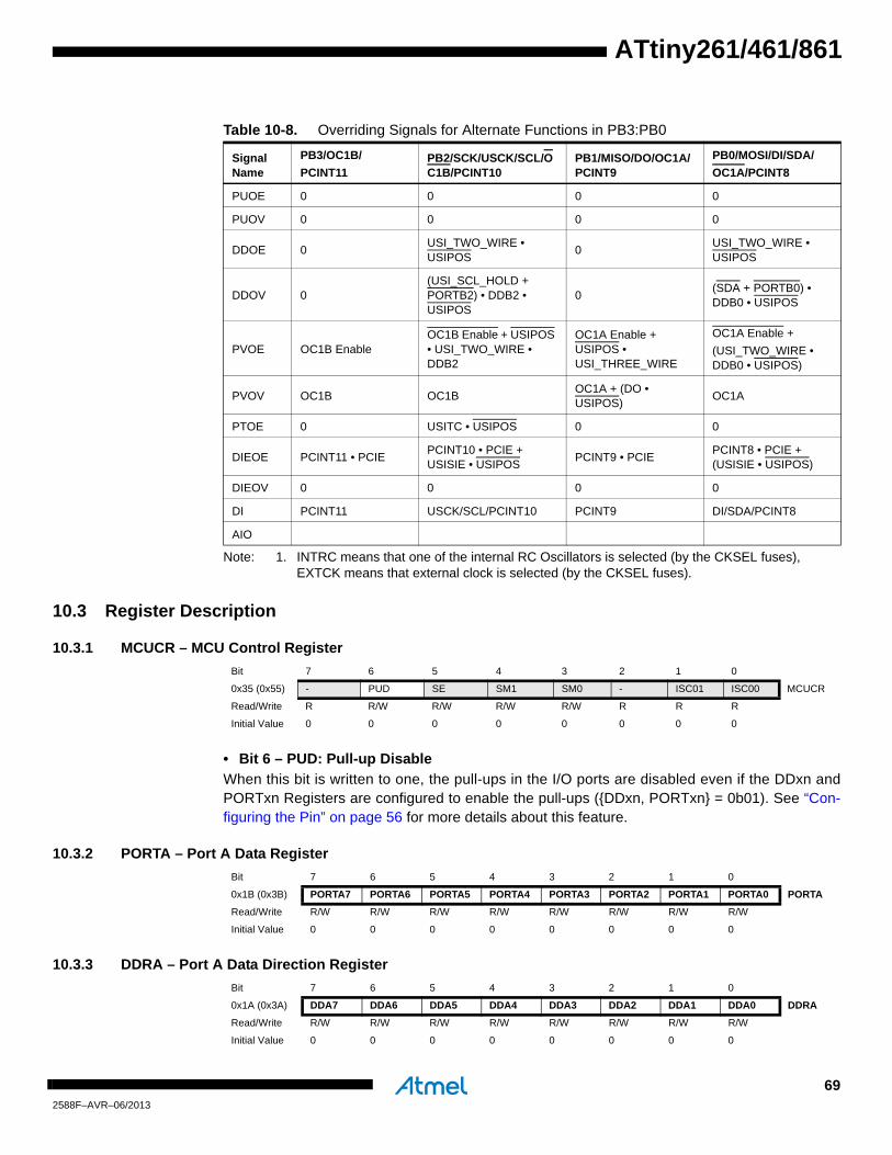
ATtiny261/461/861
Note: 1. INTRC means that one of the internal RC Oscillators is selected (by the CKSEL fuses), EXTCK means that external clock is selected (by the CKSEL fuses).
10.3 Register Description
10.3.1 MCUCR – MCU Control Register
• Bit 6 – PUD: Pull-up Disable
When this bit is written to one, the pull-ups in the I/O ports are disabled even if the DDxn andPORTxn Registers are configured to enable the pull-ups ({DDxn, PORTxn} = 0b01). See “Con-figuring the Pin” on page 56 for more details about this feature.
10.3.2 PORTA – Port A Data Register
10.3.3 DDRA – Port A Data Direction Register
Table 10-8. Overriding Signals for Alternate Functions in PB3:PB0
Signal Name
PB3/OC1B/
PCINT11PB2/SCK/USCK/SCL/OC1B/PCINT10
PB1/MISO/DO/OC1A/PCINT9
PB0/MOSI/DI/SDA/
OC1A/PCINT8
PUOE 0 0 0 0
PUOV 0 0 0 0
DDOE 0USI_TWO_WIRE • USIPOS
0USI_TWO_WIRE • USIPOS
DDOV 0(USI_SCL_HOLD + PORTB2) • DDB2 • USIPOS
0(SDA + PORTB0) • DDB0 • USIPOS
PVOE OC1B EnableOC1B Enable + USIPOS • USI_TWO_WIRE • DDB2
OC1A Enable + USIPOS • USI_THREE_WIRE
OC1A Enable +
(USI_TWO_WIRE • DDB0 • USIPOS)
PVOV OC1B OC1BOC1A + (DO • USIPOS)
OC1A
PTOE 0 USITC • USIPOS 0 0
DIEOE PCINT11 • PCIEPCINT10 • PCIE + USISIE • USIPOS
PCINT9 • PCIEPCINT8 • PCIE + (USISIE • USIPOS)
DIEOV 0 0 0 0
DI PCINT11 USCK/SCL/PCINT10 PCINT9 DI/SDA/PCINT8
AIO
Bit 7 6 5 4 3 2 1 0
0x35 (0x55) - PUD SE SM1 SM0 - ISC01 ISC00 MCUCR
Read/Write R R/W R/W R/W R/W R R R
Initial Value 0 0 0 0 0 0 0 0
Bit 7 6 5 4 3 2 1 0
0x1B (0x3B) PORTA7 PORTA6 PORTA5 PORTA4 PORTA3 PORTA2 PORTA1 PORTA0 PORTA
Read/Write R/W R/W R/W R/W R/W R/W R/W R/W
Initial Value 0 0 0 0 0 0 0 0
Bit 7 6 5 4 3 2 1 0
0x1A (0x3A) DDA7 DDA6 DDA5 DDA4 DDA3 DDA2 DDA1 DDA0 DDRA
Read/Write R/W R/W R/W R/W R/W R/W R/W R/W
Initial Value 0 0 0 0 0 0 0 0
692588F–AVR–06/2013

10.3.4 PINA – Port A Input Pins Address
10.3.5 PORTB – Port B Data Register
10.3.6 DDRB – Port B Data Direction Register
10.3.7 PINB – Port B Input Pins Address
Bit 7 6 5 4 3 2 1 0
0x19 (0x39) PINA7 PINA6 PINA5 PINA4 PINA3 PINA2 PINA1 PINA0 PINA
Read/Write R/W R/W R/W R/W R/W R/W R/W R/W
Initial Value N/A N/A N/A N/A N/A N/A N/A N/A
Bit 7 6 5 4 3 2 1 0
0x18 (0x38) PORTB7 PORTB6 PORTB5 PORTB4 PORTB3 PORTB2 PORTB1 PORTB0 PORTB
Read/Write R/W R/W R/W R/W R/W R/W R/W R/W
Initial Value 0 0 0 0 0 0 0 0
Bit 7 6 5 4 3 2 1 0
0x17 (0x37) DDB7 DDB6 DDB5 DDB4 DDB3 DDB2 DDB1 DDB0 DDRB
Read/Write R/W R/W R/W R/W R/W R/W R/W R/W
Initial Value 0 0 0 0 0 0 0 0
Bit 7 6 5 4 3 2 1 0
0x16 (0x36) PINB7 PINB6 PINB5 PINB4 PINB3 PINB2 PINB1 PINB0 PINB
Read/Write R/W R/W R/W R/W R/W R/W R/W R/W
Initial Value N/A N/A N/A N/A N/A N/A N/A N/A
702588F–AVR–06/2013
ATtiny261/461/861

ATtiny261/461/861
11. Timer/Counter0
11.1 Features• Clear Timer on Compare Match (Auto Reload)
• One Input Capture unit
• Four Independent Interrupt Sources (TOV0, OCF0A, OCF0B, ICF0)
• 8-bit Mode with Two Independent Output Compare Units
• 16-bit Mode with One Independent Output Compare Unit
11.2 OverviewTimer/Counter0 is a general purpose 8/16-bit Timer/Counter module, with two/one Output Com-pare units and Input Capture feature.
The general operation of Timer/Counter0 is described in 8/16-bit mode. A simplified block dia-gram of the 8/16-bit Timer/Counter is shown in Figure 11-1. CPU accessible I/O Registers,including I/O bits and I/O pins, are shown in bold. For actual placement of I/O pins, refer to “Pin-out ATtiny261/461/861 and ATtiny261V/461V/861V” on page 2. Device-specific I/O Register andbit locations are listed in the “Register Description” on page 84.
Figure 11-1. 8-/16-bit Timer/Counter Block Diagram
11.2.1 Registers
The Timer/Counter0 Low Byte Register (TCNT0L) and Output Compare Registers (OCR0A andOCR0B) are 8-bit registers. Interrupt request (abbreviated Int.Req. in Figure 11-1) signals are all
Clock Select
Timer/Counter
DAT
A B
US
OCRnB
=
TCNTnL
NoiseCanceler
ICPn
=
EdgeDetector
Control Logic
TOP
Count
Clear
Direction
TOVn (Int. Req.)
OCnA (Int. Req.)
OCnB (Int. Req.)
ICFn (Int. Req.)
TCCRnA TCCRnB
( From AnalogComparator Ouput )
TnEdge
Detector
( From Prescaler )
clkTn
=
OCRnA
TCNTnH
Fixed TOP value
712588F–AVR–06/2013

visible in the Timer Interrupt Flag Register (TIFR). All interrupts are individually masked with theTimer Interrupt Mask Register (TIMSK). TIFR and TIMSK are not shown in the figure.
In 16-bit mode one more 8-bit register is available, the Timer/Counter0 High Byte Register(TCNT0H). Also, in 16-bit mode, there is only one output compare unit as the two Output Com-pare Registers, OCR0A and OCR0B, are combined to one, 16-bit Output Compare Register,where OCR0A contains the low byte and OCR0B contains the high byte of the word. Whenaccessing 16-bit registers, special procedures described in section “Accessing Registers in 16-bit Mode” on page 80 must be followed.
11.2.2 Definitions
Many register and bit references in this section are written in general form. A lower case “n”replaces the Timer/Counter number, in this case 0. A lower case “x” replaces the Output Com-pare Unit, in this case Compare Unit A or Compare Unit B. However, when using the register orbit defines in a program, the precise form must be used, i.e. TCNT0L for accessingTimer/Counter0 counter value, and so on.
The definitions in Table 11-1 are also used extensively throughout the document.
11.3 Clock SourcesThe Timer/Counter can be clocked internally, via the prescaler, or by an external clock source onthe T0 pin. The Clock Select logic is controlled by the Clock Select (CS02:0) bits located in theTimer/Counter Control Register 0 B (TCCR0B), and controls which clock source and edge theTimer/Counter uses to increment its value. The Timer/Counter is inactive when no clock sourceis selected. The output from the Clock Select logic is referred to as the timer clock (clkT0).
11.3.1 Prescaler
The Timer/Counter can be clocked directly by the system clock (by setting the CSn2:0 = 1). Thisprovides the fastest operation, with a maximum Timer/Counter clock frequency equal to systemclock frequency (fCLK_I/O). Alternatively, one of four taps from the prescaler can be used as aclock source.
See Figure 11-2 for an illustration of the prescaler unit.
Table 11-1. Definitions
Constant Description
BOTTOM The counter reaches BOTTOM when it becomes 0x00
MAX The counter reaches its MAXimum when it becomes 0xFF (decimal 255)
TOPThe counter reaches the TOP when it becomes equal to the highest value in the count sequence. The TOP value can be assigned to be the fixed value 0xFF (MAX) or the value stored in the OCR0A Register. The assignment depends on the mode of operation
722588F–AVR–06/2013
ATtiny261/461/861

ATtiny261/461/861
Figure 11-2. Prescaler for Timer/Counter0
Note: 1. The synchronization logic on the input pins (T0) is shown in Figure 11-3.
The prescaled clock has a frequency of fCLK_I/O/8, fCLK_I/O/64, fCLK_I/O/256, or fCLK_I/O/1024. SeeTable 11-4 on page 85 for details.
11.3.1.1 Prescaler Reset
The prescaler is free running, i.e. it operates independently of the Clock Select logic of theTimer/Counter. Since the prescaler is not affected by the Timer/Counter’s clock select, the stateof the prescaler will have implications for situations where a prescaled clock is used. One exam-ple of prescaling artifacts occurs when the timer is enabled and clocked by the prescaler (6 >CSn2:0 > 1). The number of system clock cycles from when the timer is enabled to the first countoccurs can be from 1 to N+1 system clock cycles, where N equals the prescaler divisor (8, 64,256, or 1024). It is possible to use the Prescaler Reset for synchronizing the Timer/Counter toprogram execution.
11.3.2 External Clock Source
An external clock source applied to the T0 pin can be used as Timer/Counter clock (clkT0). TheT0 pin is sampled once every system clock cycle by the pin synchronization logic. The synchro-nized (sampled) signal is then passed through the edge detector. Figure 11-3 shows a functionalequivalent block diagram of the T0 synchronization and edge detector logic. The registers areclocked at the positive edge of the internal system clock (clkI/O). The latch is transparent in thehigh period of the internal system clock.
The edge detector generates one clkT0 pulse for each positive (CSn2:0 = 7) or negative (CSn2:0= 6) edge it detects. See Table 11-4 on page 85 for details.
PSR0
Clear
clkT0
T0
clkI/O
Synchronization
732588F–AVR–06/2013

Figure 11-3. T0 Pin Sampling
The synchronization and edge detector logic introduces a delay of 2.5 to 3.5 system clock cyclesfrom an edge has been applied to the T0 pin to the counter is updated.
Enabling and disabling of the clock input must be done when T0 has been stable for at least onesystem clock cycle, otherwise it is a risk that a false Timer/Counter clock pulse is generated.
Each half period of the external clock applied must be longer than one system clock cycle toensure correct sampling. The external clock must be guaranteed to have less than half the sys-tem clock frequency (fExtClk < fclk_I/O/2) given a 50/50% duty cycle. Since the edge detector usessampling, the maximum frequency of an external clock it can detect is half the sampling fre-quency (Nyquist sampling theorem). However, due to variation of the system clock frequencyand duty cycle caused by Oscillator source (crystal, resonator, and capacitors) tolerances, it isrecommended that maximum frequency of an external clock source is less than fclk_I/O/2.5.
An external clock source can not be prescaled.
11.4 Counter UnitThe main part of the 8-bit Timer/Counter is the programmable bi-directional counter unit. Figure11-4 shows a block diagram of the counter and its surroundings.
Table 11-2. Counter Unit Block Diagram
Signal description (internal signals):
count Increment or decrement TCNT0 by 1.clkTn Timer/Counter clock, referred to as clkT0 in the following.top Signalize that TCNT0 has reached maximum value.
The counter is incremented at each timer clock (clkT0) until it passes its TOP value and thenrestarts from BOTTOM. The counting sequence is determined by the setting of the CTC0 bitlocated in the Timer/Counter Control Register (TCCR0A). For more details about countingsequences, see “Modes of Operation” on page 77. clkT0 can be generated from an external or
Tn_sync(To ClockSelect Logic)
Edge DetectorSynchronization
D QD Q
LE
D QTn
clkI/O
DATA BUS
TCNTn Control Logiccount
TOVn(Int.Req.)
Clock Select
top
TnEdge
Detector
( From Prescaler )
clkTn
742588F–AVR–06/2013
ATtiny261/461/861

ATtiny261/461/861
internal clock source, selected by the Clock Select bits (CS02:0). When no clock source isselected (CS02:0 = 0) the timer is stopped. However, the TCNT0 value can be accessed by theCPU, regardless of whether clkT0 is present or not. A CPU write overrides (has priority over) allcounter clear or count operations. The Timer/Counter Overflow Flag (TOV0) is set when thecounter reaches the maximum value and it can be used for generating a CPU interrupt.
11.5 Input Capture UnitThe Timer/Counter incorporates an Input Capture unit that can capture external events and givethem a time-stamp indicating time of occurrence. The external signal indicating an event, or mul-tiple events, can be applied via the ICP0 pin or alternatively, via the analog-comparator unit. Thetime-stamps can then be used to calculate frequency, duty-cycle, and other features of the sig-nal applied. Alternatively the time-stamps can be used for creating a log of the events.
The Input Capture unit is illustrated by the block diagram shown in Figure 11-4. The elements ofthe block diagram that are not directly a part of the Input Capture unit are gray shaded.
Figure 11-4. Input Capture Unit Block Diagram
The Output Compare Register OCR0A is a dual-purpose register that is also used as an 8-bitInput Capture Register ICR0. In 16-bit Input Capture mode the Output Compare RegisterOCR0B serves as the high byte of the Input Capture Register ICR0. In 8-bit Input Capture modethe Output Compare Register OCR0B is free to be used as a normal Output Compare Register,but in 16-bit Input Capture mode the Output Compare Unit cannot be used as there are no freeOutput Compare Register(s). Even though the Input Capture register is called ICR0 in this sec-tion, it is refering to the Output Compare Register(s).
When a change of the logic level (an event) occurs on the Input Capture pin (ICP0), alternativelyon the Analog Comparator output (ACO), and this change confirms to the setting of the edgedetector, a capture will be triggered. When a capture is triggered, the value of the counter(TCNT0) is written to the Input Capture Register (ICR0). The Input Capture Flag (ICF0) is set at
ICF0 (Int.Req.)
AnalogComparator
WRITE ICR0 (16-bit Register)
OCR0B (8-bit)
NoiseCanceler
ICP0
EdgeDetector
TEMP (8-bit)
DATA BUS (8-bit)
OCR0A (8-bit)
TCNT0 (16-bit Counter)
TCNT0H (8-bit) TCNT0L (8-bit)
ACIC0* ICNC0 ICES0ACO*
752588F–AVR–06/2013

the same system clock as the TCNT0 value is copied into Input Capture Register. If enabled(TICIE0=1), the Input Capture Flag generates an Input Capture interrupt. The ICF0 flag is auto-matically cleared when the interrupt is executed. Alternatively the ICF0 flag can be cleared bysoftware by writing a logical one to its I/O bit location.
11.5.1 Input Capture Trigger Source
The default trigger source for the Input Capture unit is the Input Capture pin (ICP0).Timer/Counter0 can alternatively use the Analog Comparator output as trigger source for theInput Capture unit. The Analog Comparator is selected as trigger source by setting the AnalogComparator Input Capture Enable (ACIC0) bit in the Timer/Counter Control Register A(TCCR0A). Be aware that changing trigger source can trigger a capture. The Input Capture Flagmust therefore be cleared after the change.
Both the Input Capture pin (ICP0) and the Analog Comparator output (ACO) inputs are sampledusing the same technique as for the T0 pin (Figure 11-4 on page 85). The edge detector is alsoidentical. However, when the noise canceler is enabled, additional logic is inserted before theedge detector, which increases the delay by four system clock cycles. An Input Capture can alsobe triggered by software by controlling the port of the ICP0 pin.
11.5.2 Noise Canceler
The noise canceler improves noise immunity by using a simple digital filtering scheme. Thenoise canceler input is monitored over four samples, and all four must be equal for changing theoutput that in turn is used by the edge detector.
The noise canceler is enabled by setting the Input Capture Noise Canceler (ICNC0) bit inTimer/Counter Control Register B (TCCR0B). When enabled the noise canceler introduces addi-tional four system clock cycles of delay from a change applied to the input, to the update of theICR0 Register. The noise canceler uses the system clock and is therefore not affected by theprescaler.
11.5.3 Using the Input Capture Unit
The main challenge when using the Input Capture unit is to assign enough processor capacityfor handling the incoming events. The time between two events is critical. If the processor hasnot read the captured value in the ICR0 Register before the next event occurs, the ICR0 will beoverwritten with a new value. In this case the result of the capture will be incorrect.
When using the Input Capture interrupt, the ICR0 Register should be read as early in the inter-rupt handler routine as possible. The maximum interrupt response time is dependent on themaximum number of clock cycles it takes to handle any of the other interrupt requests.
Measurement of an external signal’s duty cycle requires that the trigger edge is changed aftereach capture. Changing the edge sensing must be done as early as possible after the ICR0Register has been read. After a change of the edge, the Input Capture Flag (ICF0) must becleared by software (writing a logical one to the I/O bit location). For measuring frequency only,the trigger edge change is not required (if an interrupt handler is used).
11.6 Output Compare UnitThe comparator continuously compares Timer/Counter (TCNT0) with the Output Compare Reg-isters (OCR0A and OCR0B), and whenever the Timer/Counter equals to the Output CompareRegisers, the comparator signals a match. A match will set the Output Compare Flag at the nexttimer clock cycle. In 8-bit mode the match can set either the Output Compare Flag OCF0A or
762588F–AVR–06/2013
ATtiny261/461/861

ATtiny261/461/861
OCF0B, but in 16-bit mode the match can set only the Output Compare Flag OCF0A as there isonly one Output Compare Unit. If the corresponding interrupt is enabled, the Output CompareFlag generates an Output Compare interrupt. The Output Compare Flag is automatically clearedwhen the interrupt is executed. Alternatively, the flag can be cleared by software by writing a log-ical one to its I/O bit location. Figure 11-5 shows a block diagram of the Output Compare unit.
Figure 11-5. Output Compare Unit, Block Diagram
11.6.1 Compare Match Blocking by TCNT0 Write
All CPU write operations to the TCNT0H/L Register will block any Compare Match that occur inthe next timer clock cycle, even when the timer is stopped. This feature allows OCR0A/B to beinitialized to the same value as TCNT0 without triggering an interrupt when the Timer/Counterclock is enabled.
11.6.2 Using the Output Compare Unit
Since writing TCNT0H/L will block all Compare Matches for one timer clock cycle, there are risksinvolved when changing TCNT0H/L when using the Output Compare Unit, independently ofwhether the Timer/Counter is running or not. If the value written to TCNT0H/L equals theOCR0A/B value, the Compare Match will be missed.
11.7 Modes of OperationThe mode of operation, i.e., the behavior of the Timer/Counter and the Output Compare pins, isdefined by the Timer/Counter Width (TCW0), Input Capture Enable (ICEN0) and Wave Genera-tion Mode (CTC0) bits. See “TCCR0A – Timer/Counter0 Control Register A” on page 84.
Table 11-3 summarises the different modes of operation.
OCFnx (Int.Req.)
= (8/16-bit Comparator )
OCRnx
DATA BUS
TCNTn
Table 11-3. Modes of operation
Mode ICEN0 TCW0 CTC0 Mode of Operation TOP Update of OCRx at TOV Flag Set on
0 0 0 0 Normal, 8-bit Mode 0xFF Immediate MAX (0xFF)
1 0 0 1 CTC Mode, 8-bit OCR0A Immediate MAX (0xFF)
2 0 1 X Normal, 16-bit Mode 0xFFFF Immediate MAX (0xFFFF)
3 1 0 X Input Capture Mode, 8-bit 0xFF Immediate MAX (0xFF)
4 1 1 X Input Capture Mode, 16-bit 0xFFFF Immediate MAX (0xFFFF)
772588F–AVR–06/2013

11.7.1 Normal, 8-bit Mode
In Normal 8-bit mode (see Table 11-3), the counter (TCNT0L) is incrementing until it overrunswhen it passes its maximum 8-bit value (MAX = 0xFF) and then restarts from the bottom (0x00).The Overflow Flag (TOV0) is set in the same timer clock cycle as when TCNT0L becomes zero.The TOV0 Flag in this case behaves like a ninth bit, except that it is only set, not cleared. How-ever, combined with the timer overflow interrupt that automatically clears the TOV0 Flag, thetimer resolution can be increased by software. There are no special cases to consider in theNormal 8-bit mode, a new counter value can be written anytime. The Output Compare Unit canbe used to generate interrupts at some given time.
11.7.2 Clear Timer on Compare Match (CTC) 8-bit Mode
In Clear Timer on Compare or CTC mode, see Table 11-3 on page 77, the OCR0A Register isused to manipulate the counter resolution. In CTC mode the counter is cleared to zero when thecounter value (TCNT0) matches the OCR0A. The OCR0A defines the top value for the counter,hence also its resolution. This mode allows greater control of the Compare Match output fre-quency. It also simplifies the operation of counting external events.
The timing diagram for the CTC mode is shown in Figure 11-6. The counter value (TCNT0)increases until a Compare Match occurs between TCNT0 and OCR0A, and then counter(TCNT0) is cleared.
Figure 11-6. CTC Mode, Timing Diagram
An interrupt can be generated each time the counter value reaches the TOP value by using theOCF0A Flag. If the interrupt is enabled, the interrupt handler routine can be used for updatingthe TOP value. However, changing TOP to a value close to BOTTOM when the counter is run-ning with none or a low prescaler value must be done with care since the CTC mode does nothave the double buffering feature. If the new value written to OCR0A is lower than the currentvalue of TCNT0, the counter will miss the Compare Match. The counter will then have to count toits maximum value (0xFF) and wrap around starting at 0x00 before the Compare Match canoccur. As for the Normal mode of operation, the TOV0 Flag is set in the same timer clock cyclethat the counter counts from MAX to 0x00.
11.7.3 Normal, 16-bit Mode
In 16-bit mode, see Table 11-3 on page 77, the counter (TCNT0H/L) is a incrementing until itoverruns when it passes its maximum 16-bit value (MAX = 0xFFFF) and then restarts from thebottom (0x0000). The Overflow Flag (TOV0) will be set in the same timer clock cycle as theTCNT0H/L becomes zero. The TOV0 Flag in this case behaves like a 17th bit, except that it isonly set, not cleared. However, combined with the timer overflow interrupt that automaticallyclears the TOV0 Flag, the timer resolution can be increased by software. There are no special
TCNTn
OCnx Interrupt Flag Set
1 4Period 2 3
782588F–AVR–06/2013
ATtiny261/461/861

ATtiny261/461/861
cases to consider in the Normal mode, a new counter value can be written anytime. The OutputCompare Unit can be used to generate interrupts at some given time.
11.7.4 8-bit Input Capture Mode
The Timer/Counter0 can also be used in an 8-bit Input Capture mode, see Table 11-3 on page77 for bit settings. For full description, see the section “Input Capture Unit” on page 75.
11.7.5 16-bit Input Capture Mode
The Timer/Counter0 can also be used in a 16-bit Input Capture mode, see Table 11-3 on page77 for bit settings. For full description, see the section “Input Capture Unit” on page 75.
11.8 Timer/Counter Timing DiagramsThe Timer/Counter is a synchronous design and the timer clock (clkT0) is therefore shown as aclock enable signal in the following figures. The figures include information on when InterruptFlags are set. Figure 11-7 contains timing data for basic Timer/Counter operation. The figureshows the count sequence close to the MAX value.
Figure 11-7. Timer/Counter Timing Diagram, no Prescaling
Figure 11-8 shows the same timing data, but with the prescaler enabled.
Figure 11-8. Timer/Counter Timing Diagram, with Prescaler (fclk_I/O/8)
Figure 11-9 on page 80 shows the setting of OCF0A and OCF0B in Normal mode.
clkTn(clkI/O/1)
TOVn
clkI/O
TCNTn MAX - 1 MAX BOTTOM BOTTOM + 1
TOVn
TCNTn MAX - 1 MAX BOTTOM BOTTOM + 1
clkI/O
clkTn(clkI/O/8)
792588F–AVR–06/2013

Figure 11-9. Timer/Counter Timing Diagram, Setting of OCF0x, with Prescaler (fclk_I/O/8)
Figure 11-10 shows the setting of OCF0A and the clearing of TCNT0 in CTC mode.
Figure 11-10. Timer/Counter Timing Diagram, CTC mode, with Prescaler (fclk_I/O/8)
11.9 Accessing Registers in 16-bit ModeIn 16-bit mode (the TCW0 bit is set to one) the TCNT0H/L and OCR0A/B or TCNT0L/H andOCR0B/A are 16-bit registers that can be accessed by the AVR CPU via the 8-bit data bus. The16-bit register must be byte accessed using two read or write operations. The 16-bitTimer/Counter has a single 8-bit register for temporary storing of the high byte of the 16-bitaccess. The same temporary register is shared between all 16-bit registers. Accessing the lowbyte triggers the 16-bit read or write operation. When the low byte of a 16-bit register is writtenby the CPU, the high byte stored in the temporary register, and the low byte written are both cop-ied into the 16-bit register in the same clock cycle. When the low byte of a 16-bit register is readby the CPU, the high byte of the 16-bit register is copied into the temporary register in the sameclock cycle as the low byte is read.
There is one exception in the temporary register usage. In the Output Compare mode the 16-bitOutput Compare Register OCR0A/B is read without the temporary register, because the OutputCompare Register contains a fixed value that is only changed by CPU access. However, in 16-bit Input Capture mode the ICR0 register formed by the OCR0A and OCR0B registers must beaccessed with the temporary register.
To do a 16-bit write, the high byte must be written before the low byte. For a 16-bit read, the lowbyte must be read before the high byte.
OCFnx
OCRnx
TCNTn
OCRnx Value
OCRnx - 1 OCRnx OCRnx + 1 OCRnx + 2
clkI/O
clkTn(clkI/O/8)
OCFnx
OCRnx
TCNTn(CTC)
TOP
TOP - 1 TOP BOTTOM BOTTOM + 1
clkPCK
clkTn(clkPCK /8)
802588F–AVR–06/2013
ATtiny261/461/861

ATtiny261/461/861
The following code examples show how to access the 16-bit timer registers assuming that nointerrupts updates the temporary register. The same principle can be used directly for accessingthe OCR0A/B registers.
Note: See “Code Examples” on page 6.
The assembly code example returns the TCNT0H/L value in the r17:r16 register pair.
It is important to notice that accessing 16-bit registers are atomic operations. If an interruptoccurs between the two instructions accessing the 16-bit register, and the interrupt codeupdates the temporary register by accessing the same or any other of the 16-bit timer registers,then the result of the access outside the interrupt will be corrupted. Therefore, when both themain code and the interrupt code update the temporary register, the main code must disable theinterrupts during the 16-bit access.
Assembly Code Example
...
; Set TCNT0 to 0x01FF
ldi r17,0x01
ldi r16,0xFF
out TCNT0H,r17
out TCNT0L,r16
; Read TCNT0 into r17:r16
in r16,TCNT0L
in r17,TCNT0H
...
C Code Example
unsigned int i;
...
/* Set TCNT0 to 0x01FF */
TCNT0H = 0x01;
TCNT0L = 0xff;
/* Read TCNT0 into i */
i = TCNT0L;
i |= ((unsigned int)TCNT0H << 8);
...
812588F–AVR–06/2013

The following code examples show how to do an atomic read of the TCNT0 register contents.Reading any of the OCR0 register can be done by using the same principle.
Note: See “Code Examples” on page 6.
The assembly code example returns the TCNT0H/L value in the r17:r16 register pair.
Assembly Code Example
TIM0_ReadTCNT0:
; Save global interrupt flag
in r18,SREG
; Disable interrupts
cli
; Read TCNT0 into r17:r16
in r16,TCNT0L
in r17,TCNT0H
; Restore global interrupt flag
out SREG,r18
ret
C Code Example
unsigned int TIM0_ReadTCNT0( void )
{
unsigned char sreg;
unsigned int i;
/* Save global interrupt flag */
sreg = SREG;
/* Disable interrupts */
_CLI();
/* Read TCNT0 into i */
i = TCNT0L;
i |= ((unsigned int)TCNT0H << 8);
/* Restore global interrupt flag */
SREG = sreg;
return i;
}
822588F–AVR–06/2013
ATtiny261/461/861
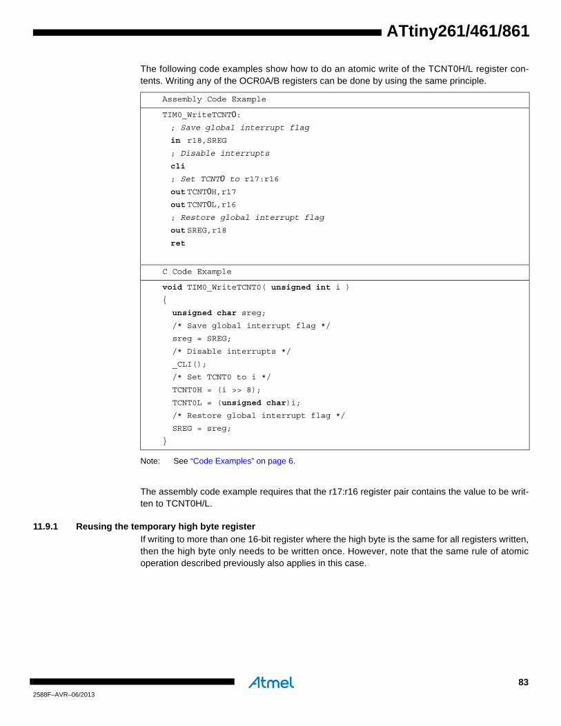
ATtiny261/461/861
The following code examples show how to do an atomic write of the TCNT0H/L register con-tents. Writing any of the OCR0A/B registers can be done by using the same principle.
Note: See “Code Examples” on page 6.
The assembly code example requires that the r17:r16 register pair contains the value to be writ-ten to TCNT0H/L.
11.9.1 Reusing the temporary high byte register
If writing to more than one 16-bit register where the high byte is the same for all registers written,then the high byte only needs to be written once. However, note that the same rule of atomicoperation described previously also applies in this case.
Assembly Code Example
TIM0_WriteTCNT0:
; Save global interrupt flag
in r18,SREG
; Disable interrupts
cli
; Set TCNT0 to r17:r16
out TCNT0H,r17
out TCNT0L,r16
; Restore global interrupt flag
out SREG,r18
ret
C Code Example
void TIM0_WriteTCNT0( unsigned int i )
{
unsigned char sreg;
/* Save global interrupt flag */
sreg = SREG;
/* Disable interrupts */
_CLI();
/* Set TCNT0 to i */
TCNT0H = (i >> 8);
TCNT0L = (unsigned char)i;
/* Restore global interrupt flag */
SREG = sreg;
}
832588F–AVR–06/2013

11.10 Register Description
11.10.1 TCCR0A – Timer/Counter0 Control Register A
• Bit 7 – TCW0: Timer/Counter0 Width
When this bit is written to one 16-bit mode is selected as described Figure 11-7 on page 79.Timer/Counter0 width is set to 16-bits and the Output Compare Registers OCR0A and OCR0Bare combined to form one 16-bit Output Compare Register. Because the 16-bit registersTCNT0H/L and OCR0B/A are accessed by the AVR CPU via the 8-bit data bus, special proce-dures must be followed. These procedures are described in section “Accessing Registers in 16-bit Mode” on page 80.
• Bit 6 – ICEN0: Input Capture Mode Enable
When this bit is written to onem, the Input Capture Mode is enabled.
• Bit 5 – ICNC0: Input Capture Noise Canceler
Setting this bit activates the Input Capture Noise Canceler. When the noise canceler is acti-vated, the input from the Input Capture Pin (ICP0) is filtered. The filter function requires foursuccessive equal valued samples of the ICP0 pin for changing its output. The Input Capture istherefore delayed by four System Clock cycles when the noise canceler is enabled.
• Bit 4 – ICES0: Input Capture Edge Select
This bit selects which edge on the Input Capture Pin (ICP0) that is used to trigger a captureevent. When the ICES0 bit is written to zero, a falling (negative) edge is used as trigger, andwhen the ICES0 bit is written to one, a rising (positive) edge will trigger the capture. When a cap-ture is triggered according to the ICES0 setting, the counter value is copied into the InputCapture Register. The event will also set the Input Capture Flag (ICF0), and this can be used tocause an Input Capture Interrupt, if this interrupt is enabled.
• Bit 3 - ACIC0: Analog Comparator Input Capture Enable
When written logic one, this bit enables the input capture function in Timer/Counter0 to be trig-gered by the Analog Comparator. The comparator output is in this case directly connected to theinput capture front-end logic, making the comparator utilize the noise canceler and edge selectfeatures of the Timer/Counter0 Input Capture interrupt. When written logic zero, no connectionbetween the Analog Comparator and the input capture function exists. To make the comparatortrigger the Timer/Counter0 Input Capture interrupt, the TICIE0 bit in the Timer Interrupt MaskRegister (TIMSK) must be set.
• Bits 2:1 – Res: Reserved Bits
These bits are reserved and will always read zero.
• Bit 0 – CTC0: Waveform Generation Mode
This bit controls the counting sequence of the counter, the source for maximum (TOP) countervalue, see Figure 11-7 on page 79. Modes of operation supported by the Timer/Counter unit are:Normal mode (counter) and Clear Timer on Compare Match (CTC) mode (see “Modes of Oper-ation” on page 77).
Bit 7 6 5 4 3 2 1 0
0x15 (0x35) TCW0 ICEN0 ICNC0 ICES0 ACIC0 – – CTC0 TCCR0A
Read/Write R/W R/W R/W R/W R/W R R R/W
Initial Value 0 0 0 0 0 0 0 0
842588F–AVR–06/2013
ATtiny261/461/861

ATtiny261/461/861
11.10.2 TCCR0B – Timer/Counter0 Control Register B
• Bit 4 – TSM: Timer/Counter Synchronization Mode
Writing the TSM bit to one activates the Timer/Counter Synchronization mode. In this mode, thevalue that is written to the PSR0 bit is kept, hence keeping the Prescaler Reset signal asserted.This ensures that the Timer/Counter is halted and can be configured without the risk of advanc-ing during configuration. When the TSM bit is written to zero, the PSR0 bit is cleared byhardware, and the Timer/Counter start counting.
• Bit 3 – PSR0: Prescaler Reset Timer/Counter0
When this bit is one, the Timer/Counter0 prescaler will be Reset. This bit is normally clearedimmediately by hardware, except if the TSM bit is set.
• Bits 2:0 – CS02, CS01, CS00: Clock Select0, Bit 2, 1, and 0
The Clock Select0 bits 2, 1, and 0 define the prescaling source of Timer0.
If external pin modes are used for the Timer/Counter0, transitions on the T0 pin will clock thecounter even if the pin is configured as an output. This feature allows software control of thecounting.
11.10.3 TCNT0L – Timer/Counter0 Register Low Byte
The Timer/Counter0 Register Low Byte, TCNT0L, gives direct access, both for read and writeoperations, to the Timer/Counter unit 8-bit counter. Writing to the TCNT0L Register blocks (dis-ables) the Compare Match on the following timer clock. Modifying the counter (TCNT0L) whilethe counter is running, introduces a risk of missing a Compare Match between TCNT0L and theOCR0x Registers. In 16-bit mode the TCNT0L register contains the lower part of the 16-bitTimer/Counter0 Register.
Bit 7 6 5 4 3 2 1 0
0x33 (0x53) - - - TSM PSR0 CS02 CS01 CS01 TCCR0B
Read/Write R R R R/W R/W R/W R/W R/W
Initial Value 0 0 0 0 0 0 0 0
Table 11-4. Clock Select Bit Description
CS02 CS01 CS00 Description
0 0 0 No clock source (Timer/Counter stopped)
0 0 1 clkI/O/(No prescaling)
0 1 0 clkI/O/8 (From prescaler)
0 1 1 clkI/O/64 (From prescaler)
1 0 0 clkI/O/256 (From prescaler)
1 0 1 clkI/O/1024 (From prescaler)
1 1 0 External clock source on T0 pin. Clock on falling edge.
1 1 1 External clock source on T0 pin. Clock on rising edge.
Bit 7 6 5 4 3 2 1 0
0x32 (0x52) TCNT0L[7:0] TCNT0L
Read/Write R/W R/W R/W R/W R/W R/W R/W R/W
Initial Value 0 0 0 0 0 0 0 0
852588F–AVR–06/2013

11.10.4 TCNT0H – Timer/Counter0 Register High Byte
When 16-bit mode is selected (the TCW0 bit is set to one) the Timer/Counter Register TCNT0Hcombined to the Timer/Counter Register TCNT0L gives direct access, both for read and writeoperations, to the Timer/Counter unit 16-bit counter. To ensure that both the high and low bytesare read and written simultaneously when the CPU accesses these registers, the access is per-formed using an 8-bit temporary high byte register (TEMP). This temporary register is shared byall the other 16-bit registers. See “Accessing Registers in 16-bit Mode” on page 80
11.10.5 OCR0A – Timer/Counter0 Output Compare Register A
The Output Compare Register A contains an 8-bit value that is continuously compared with thecounter value (TCNT0L). A match can be used to generate an Output Compare interrupt.
In 16-bit mode the OCR0A register contains the low byte of the 16-bit Output Compare Register.To ensure that both the high and the low bytes are written simultaneously when the CPU writesto these registers, the access is performed using an 8-bit temporary high byte register (TEMP).This temporary register is shared by all the other 16-bit registers. See “Accessing Registers in16-bit Mode” on page 80.
11.10.6 OCR0B – Timer/Counter0 Output Compare Register B
The Output Compare Register B contains an 8-bit value that is continuously compared with thecounter value (TCNT0L in 8-bit mode and TCNTH in 16-bit mode). A match can be used to gen-erate an Output Compare interrupt.
In 16-bit mode the OCR0B register contains the high byte of the 16-bit Output Compare Regis-ter. To ensure that both the high and the low bytes are written simultaneously when the CPUwrites to these registers, the access is performed using an 8-bit temporary high byte register(TEMP). This temporary register is shared by all the other 16-bit registers. See “Accessing Reg-isters in 16-bit Mode” on page 80.
11.10.7 TIMSK – Timer/Counter0 Interrupt Mask Register
• Bit 4 – OCIE0A: Timer/Counter0 Output Compare Match A Interrupt Enable
When the OCIE0A bit is written to one, and the I-bit in the Status Register is set, theTimer/Counter0 Compare Match A interrupt is enabled. The corresponding interrupt is executed
Bit 7 6 5 4 3 2 1 0
0x14 (0x34) TCNT0H[7:0] TCNT0H
Read/Write R/W R/W R/W R/W R/W R/W R/W R/W
Initial Value 0 0 0 0 0 0 0 0
Bit 7 6 5 4 3 2 1 0
0x13 (0x33) OCR0A[7:0] OCR0A
Read/Write R/W R/W R/W R/W R/W R/W R/W R/W
Initial Value 0 0 0 0 0 0 0 0
Bit 7 6 5 4 3 2 1 0
0x12 (0x32) OCR0B[7:0] OCR0B
Read/Write R/W R/W R/W R/W R/W R/W R/W R/W
Initial Value 0 0 0 0 0 0 0 0
Bit 7 6 5 4 3 2 1 0
0x39 (0x59) OCIE1D OCIE1A OCIE1B OCIE0A OCIE0B TOIE1 TOIE0 TICIE0 TIMSK
Read/Write R/W R/W R/W R/W R/W R/W R/W R
Initial Value 0 0 0 0 0 0 0 0
862588F–AVR–06/2013
ATtiny261/461/861

ATtiny261/461/861
if a Compare Match in Timer/Counter0 occurs, i.e., when the OCF0A bit is set in theTimer/Counter 0 Interrupt Flag Register – TIFR0.
• Bit 3 – OCIE0B: Timer/Counter Output Compare Match B Interrupt Enable
When the OCIE0B bit is written to one, and the I-bit in the Status Register is set, theTimer/Counter Compare Match B interrupt is enabled. The corresponding interrupt is executed ifa Compare Match in Timer/Counter occurs, i.e., when the OCF0B bit is set in the Timer/CounterInterrupt Flag Register – TIFR0.
• Bit 1 – TOIE0: Timer/Counter0 Overflow Interrupt Enable
When the TOIE0 bit is written to one, and the I-bit in the Status Register is set, theTimer/Counter0 Overflow interrupt is enabled. The corresponding interrupt is executed if anoverflow in Timer/Counter0 occurs, i.e., when the TOV0 bit is set in the Timer/Counter 0 Inter-rupt Flag Register – TIFR0.
• Bit 0 – TICIE0: Timer/Counter0, Input Capture Interrupt Enable
When this bit is written to one, and the I-flag in the Status Register is set (interrupts globallyenabled), the Timer/Counter1 Input Capture interrupt is enabled. The corresponding InterruptVector (See “Interrupts” on page 50.) is executed when the ICF0 flag, located in TIFR, is set.
11.10.8 TIFR – Timer/Counter0 Interrupt Flag Register
• Bit 4 – OCF0A: Output Compare Flag 0 A
The OCF0A bit is set when a Compare Match occurs between the Timer/Counter0 and the datain OCR0A – Output Compare Register0. OCF0A is cleared by hardware when executing the cor-responding interrupt handling vector. Alternatively, OCF0A is cleared by writing a logic one tothe flag. When the I-bit in SREG, OCIE0A (Timer/Counter0 Compare Match Interrupt Enable),and OCF0A are set, the Timer/Counter0 Compare Match Interrupt is executed.
The OCF0A is also set in 16-bit mode when a Compare Match occurs between the Timer/Coun-ter and 16-bit data in OCR0B/A. The OCF0A is not set in Input Capture mode when the OutputCompare Register OCR0A is used as an Input Capture Register.
• Bit 3 – OCF0B: Output Compare Flag 0 B
The OCF0B bit is set when a Compare Match occurs between the Timer/Counter and the data inOCR0B – Output Compare Register0 B. OCF0B is cleared by hardware when executing the cor-responding interrupt handling vector. Alternatively, OCF0B is cleared by writing a logic one tothe flag. When the I-bit in SREG, OCIE0B (Timer/Counter Compare B Match Interrupt Enable),and OCF0B are set, the Timer/Counter Compare Match Interrupt is executed.
The OCF0B is not set in 16-bit Output Compare mode when the Output Compare RegisterOCR0B is used as the high byte of the 16-bit Output Compare Register or in 16-bit Input Cap-ture mode when the Output Compare Register OCR0B is used as the high byte of the InputCapture Register.
Bit 7 6 5 4 3 2 1 0
0x38 (0x58) OCF1D OCF1A OCF1B OCF0A OCF0B TOV1 TOV0 ICF0 TIFR
Read/Write R/W R/W R/W R/W R/W R/W R/W R
Initial Value 0 0 0 0 0 0 0 0
872588F–AVR–06/2013
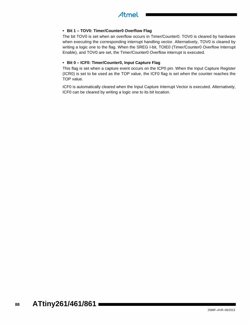
• Bit 1 – TOV0: Timer/Counter0 Overflow Flag
The bit TOV0 is set when an overflow occurs in Timer/Counter0. TOV0 is cleared by hardwarewhen executing the corresponding interrupt handling vector. Alternatively, TOV0 is cleared bywriting a logic one to the flag. When the SREG I-bit, TOIE0 (Timer/Counter0 Overflow InterruptEnable), and TOV0 are set, the Timer/Counter0 Overflow interrupt is executed.
• Bit 0 – ICF0: Timer/Counter0, Input Capture Flag
This flag is set when a capture event occurs on the ICP0 pin. When the Input Capture Register(ICR0) is set to be used as the TOP value, the ICF0 flag is set when the counter reaches theTOP value.
ICF0 is automatically cleared when the Input Capture Interrupt Vector is executed. Alternatively,ICF0 can be cleared by writing a logic one to its bit location.
882588F–AVR–06/2013
ATtiny261/461/861

ATtiny261/461/861
12. Timer/Counter1
12.1 Features• 8/10-Bit Accuracy
• Three Independent Output Compare Units
• Clear Timer on Compare Match (Auto Reload)
• Glitch Free, Phase and Frequency Correct Pulse Width Modulator (PWM)
• Variable PWM Period
• High Speed Asynchronous and Synchronous Clocking with Dedicated Prescaler
• Independent Dead Time Generators for Each PWM Channel
• Fault Protection Unit Can Disable PWM Output Pins
• Five Independent Interrupt Sources (TOV1, OCF1A, OCD1B, OCF1D, FPF1)
12.2 OverviewTimer/Counter1 is a general purpose high speed Timer/Counter module, with three independentOutput Compare Units, and with PWM support.
The Timer/Counter1 features a high resolution and a high accuracy usage with the lower presca-ling opportunities. It can also support three accurate and high speed Pulse Width Modulatorsusing clock speeds up to 64 MHz. In PWM mode Timer/Counter1 and the output compare regis-ters serve as triple stand-alone PWMs with non-overlapping non-inverted and inverted outputs.Similarly, the high prescaling opportunities make this unit useful for lower speed functions orexact timing functions with infrequent actions. A simplified block diagram of the Timer/Counter1is shown in Figure 12-1.
Figure 12-1. Timer/Counter1 Block Diagram
8-BIT DATABUS
T/C INT. FLAGREGISTER (TIFR)
10-BIT COMPARATOR
8-BIT OUTPUT COMPARE REGISTER A (OCR1A)
T/C INT. MASKREGISTER (TIMSK)
TIMER/COUNTER1 (TCNT1)
DIRECTION
TIMER/COUNTER1 CONTROL LOGIC
OC
F1B
TO
V1
TO
IE1
OC
IE1B
OC
IE1A
OC
F1A
TOV1 OCF1B OC1AOCF1A
T/C CONTROLREGISTER A (TCCR1A)
CO
M1B
1
PW
M1A
PW
M1B
CO
M1B
0
FO
C1A
FO
C1B
10-BIT COMPARATOR
8-BIT OUTPUT COMPARE REGISTER B (OCR1B)
CO
M1A
1
CO
M1A
0
T/C CONTROLREGISTER B (TCCR1B)
CS
12
PS
R1
CS
11
CS
10
CS
13
OC1A OC1B OC1B
DEAD TIME GENERATOR DEAD TIME GENERATOR
10-BIT COMPARATOR
8-BIT OUTPUT COMPARE REGISTER C (OCR1C)
10-BIT COMPARATOR
8-BIT OUTPUT COMPARE REGISTER D (OCR1D)
CO
M1A
1
PW
M1D
CO
M1A
0
FO
C1D
T/C CONTROLREGISTER C (TCCR1C)
OCF1D
OC
F1D
OC
IE1D
OC1D OC1D
DEAD TIME GENERATOR
PS
R1
PS
R1
OCW1A
OCW1B
OCW1D
2-BIT HIGH BYTEREGISTER (TC1H)
WG
M11
FP
EN
1
T/C CONTROLREGISTER D (TCCR1E)
CO
M1B
1
CO
M1B
0
CO
M1D
1
CO
M1D
0
FP
NC
1
FP
ES
1
FP
AC
1
10-BIT OUTPUTCOMPARE REGISTER B
10-BIT OUTPUTCOMPARE REGISTER C
10-BIT OUTPUTCOMPARE REGISTER D
10-BIT OUTPUTCOMPARE REGISTER A
CLEAR
COUNT
CLK
T/C CONTROLREGISTER C (TCCR1D)
FAULT_PROTECTION
WG
M10
FP
IE1
FP
F1
OC
1OE
5
OC
1OE
4
OC
1OE
3
OC
1OE
2
OC
1OE
1
OC
1OE
0
FP
IE1
FP
F1
892588F–AVR–06/2013

For actua l p lacement o f the I /O p ins, re fer to “P inout ATt iny261/461/861 andATtiny261V/461V/861V” on page 2. The device-specific I/O register and bit locations are listedin the “Register Description” on page 112.
12.2.1 Speed
The maximum speed of the Timer/Counter1 is 64 MHz. However, if a supply voltage below 2.7volts is used, it is recommended to use the Low Speed Mode (LSM), because theTimer/Counter1 is not running fast enough on low voltage levels. In the Low Speed Mode thefast peripheral clock is scaled down to 32 MHz. For more details about the Low Speed Mode,see “PLLCSR – PLL Control and Status Register” on page 120.
12.2.2 Accuracy
The Timer/Counter1 is a 10-bit Timer/Counter module that can alternatively be used as an 8-bitTimer/Counter. The Timer/Counter1 registers are basically 8-bit registers, but on top of thatthere is a 2-bit High Byte Register (TC1H) that can be used as a common temporary buffer toaccess the two MSBs of the 10-bit Timer/Counter1 registers by the AVR CPU via the 8-bit databus, if the 10-bit accuracy is used. Whereas, if the two MSBs of the 10-bit registers are written tozero the Timer/Counter1 is working as an 8-bit Timer/Counter. When reading the low byte of any8-bit register the two MSBs are written to the TC1H register, and when writing the low byte ofany 8-bit register the two MSBs are written from the TC1H register. Special procedures must befollowed when accessing the 10-bit Timer/Counter1 values via the 8-bit data bus. These proce-dures are described in the section “Accessing 10-Bit Registers” on page 108.
12.2.3 Registers
The Timer/Counter (TCNT1) and Output Compare Registers (OCR1A, OCR1B, OCR1C andOCR1D) are 8-bit registers that are used as a data source to be compared with the TCNT1 con-tents. The OCR1A, OCR1B and OCR1D registers determine the action on the OC1A, OC1B andOC1D pins and they can also generate the compare match interrupts. The OCR1C holds theTimer/Counter TOP value, i.e. the clear on compare match value. The Timer/Counter1 HighByte Register (TC1H) is a 2-bit register that is used as a common temporary buffer to access theMSB bits of the Timer/Counter1 registers, if the 10-bit accuracy is used.
Interrupt request (overflow TOV1, and compare matches OCF1A, OCF1B, OCF1D and fault pro-tection FPF1) signals are visible in the Timer Interrupt Flag Register (TIFR) and Timer/Counter1Control Register D (TCCR1D). The interrupts are individually masked with the Timer InterruptMask Register (TIMSK) and the FPIE1 bit in the Timer/Counter1 Control Register D (TCCR1D).
Control signals are found in the Timer/Counter Control Registers TCCR1A, TCCR1B, TCCR1C,TCCR1D and TCCR1E.
12.2.4 Synchronization
In asynchronous clocking mode the Timer/Counter1 and the prescaler allow running the CPUfrom any clock source while the prescaler is operating on the fast peripheral clock (PCK) havingfrequency of 64 MHz (or 32 MHz in Low Speed Mode). This is possible because there is a syn-chronization boundary between the CPU clock domain and the fast peripheral clock domain.Figure 12-2 shows Timer/Counter 1 synchronization register block diagram and describes syn-chronization delays in between registers. Note that all clock gating details are not shown in thefigure.
The Timer/Counter1 register values go through the internal synchronization registers, whichcause the input synchronization delay, before affecting the counter operation. The registers
902588F–AVR–06/2013
ATtiny261/461/861

ATtiny261/461/861
TCCR1A, TCCR1B, TCCR1C, TCCR1D, OCR1A, OCR1B, OCR1C and OCR1D can be readback right after writing the register. The read back values are delayed for the Timer/Counter1(TCNT1) register, Timer/Counter1 High Byte Register (TC1H) and flags (OCF1A, OCF1B,OCF1D and TOV1), because of the input and output synchronization.
The system clock frequency must be lower than half of the PCK frequency, because the syn-chronization mechanism of the asynchronous Timer/Counter1 needs at least two edges of thePCK when the system clock is high. If the frequency of the system clock is too high, it is a riskthat data or control values are lost.
Figure 12-2. Timer/Counter1 Synchronization Register Block Diagram.
12.2.5 Definitions
Many register and bit references in this section are written in general form. A lower case “n”replaces the Timer/Counter number, in this case 0. A lower case “x” replaces the Output Com-pare Unit, in this case Compare Unit A, B, C or D. However, when using the register or bitdefines in a program, the precise form must be used, i.e., TCNT1 for accessing Timer/Counter1
8-BIT DATABUS
OCR1A OCR1A_SI
TCNT1_SOOCR1B OCR1B_SI
OCR1C OCR1C_SI
TCCR1A TCCR1A_SI
TCCR1B TCCR1B_SI
TCNT1 TCNT1_SI
OCF1A OCF1A_SI
OCF1B OCF1B_SI
TOV1 TOV1_SI TOV1_SO
OCF1B_SO
OCF1A_SO
TCNT1
S
AS
A
PCKE
CK
PCK
IO-registers Input synchronizationregisters
Timer/Counter1 Output synchronizationregisters
SYNCMODE
ASYNCMODE
1 CK Delay 1/2 CK Delay
~1/2 CK Delay 1 PCK Delay 1 PCK Delay ~1 CK Delay
TCNT1
OCF1A
OCF1B
TOV1
1/2 CK Delay 1 CK Delay
OCR1D OCR1D_SI
TC1H TC1H_SI
TCCR1C TCCR1C_SI
TCCR1D
OCF1D OCF1D_SI
OCF1D_SOOCF1D
TC1H_SOTC1H
TCCR1D_SI
912588F–AVR–06/2013

counter value and so on. The definitions in Table 12-1 are used extensively throughout thedocument.
12.3 Clock SourcesThe Timer/Counter is clocked internally, either from CK or PCK. See bits CSxx in Table 12-17 onpage 116 and bit PCKE in “PLLCSR – PLL Control and Status Register” on page 120.
12.3.1 Prescaler
Figure 12-3 shows the Timer/Counter1 prescaler that supports two clocking modes, a synchro-nous clocking mode and an asynchronous clocking mode. The synchronous clocking mode usesthe system clock (CK) as a clock timebase and asynchronous mode uses the fast peripheralclock (PCK) as a clock time base. The PCKE bit from the PLLCSR register enables the asyn-chronous mode when it is set (‘1’).
Figure 12-3. Timer/Counter1 Prescaler
In the asynchronous clocking mode the clock selections are from PCK to PCK/16384 and stop,and in the synchronous clocking mode the clock selections are from CK to CK/16384 and stop.The clock options are illustrated in Figure 12-3 and desribed in “TCCR1B – Timer/Counter1Control Register B” on page 115.
The frequency of the fast peripheral clock is 64 MHz or 32 MHz in Low Speed mode (the LSM bitin PLLCSR register is set to one). The Low Speed Mode is recommended to use when the sup-ply voltage below 2.7 volts are used.
Table 12-1. Definitions
Constant Description
BOTTOM The counter reaches BOTTOM when it becomes 0x00
MAX The counter reaches its MAXimum when it becomes 0xFF (decimal 255)
TOPThe counter reaches the TOP when it becomes equal to the highest value in the count sequence. The TOP value can be assigned to be the fixed value 0xFF (MAX) or the value stored in the OCR0A Register. The assignment depends on the mode of operation
TIMER/COUNTER1 COUNT ENABLE
PSR1
CS10CS11CS12
PCK 64/32 MHz
0
CS13
14-BITT/C PRESCALER
T1C
K/2
T1C
K
T1C
K/4
T1C
K/8
T1C
K/1
6
T1C
K/3
2
T1C
K/6
4
T1C
K/1
28
T1C
K/2
56
T1C
K/5
12
T1C
K/1
024
T1C
K/2
048
T1C
K/4
096
T1C
K/8
192
T1C
K/1
6384
SA
CK
PCKE
T1CK
922588F–AVR–06/2013
ATtiny261/461/861

ATtiny261/461/861
12.3.1.1 Prescaler Reset
Setting the PSR1 bit in TCCR1B register resets the prescaler. It is possible to use the PrescalerReset for synchronizing the Timer/Counter to program execution.
12.3.1.2 Prescaler Initialization for Asynchronous Mode
To change Timer/Counter1 to the asynchronous mode follow the procedure below:
1. Enable PLL.
2. Wait 100 µs for PLL to stabilize.
3. Poll the PLOCK bit until it is set.
4. Set the PCKE bit in the PLLCSR register which enables the asynchronous mode.
12.4 Counter UnitThe main part of the Timer/Counter1 is the programmable bi-directional counter unit. Figure 12-4 shows a block diagram of the counter and its surroundings.
Figure 12-4. Counter Unit Block Diagram
Signal description (internal signals):
count TCNT1 increment or decrement enable.direction Select between increment and decrement.clear Clear TCNT1 (set all bits to zero).clkTn Timer/Counter clock, referred to as clkT1 in the following.top Signalize that TCNT1 has reached maximum value.bottom Signalize that TCNT1 has reached minimum value (zero).
Depending on the mode of operation used, the counter is cleared, incremented, or decrementedat each timer clock (clkT1). The timer clock is generated from an synchronous system clock or anasynchronous PLL clock using the Clock Select bits (CS13:0) and the PCK Enable bit (PCKE).When no clock source is selected (CS13:0 = 0) the timer is stopped. However, the TCNT1 valuecan be accessed by the CPU, regardless of whether clkT1 is present or not. A CPU write over-rides (has priority over) all counter clear or count operations.
The counting sequence of the Timer/Counter1 is determined by bits WGM11:10, PWM1A andPWM1B, located in the Timer/Counter1 Control Registers (TCCR1A, TCCR1C and TCCR1D).For more details about advanced counting sequences and waveform generation, see “Modes ofOperation” on page 99. The Timer/Counter Overflow Flag (TOV1) is set according to the modeof operation and can be used for generating a CPU interrupt.
DATA BUS
TCNT1 Control Logic
count
TOV1
top
Timer/Counter1 Count Enable ( From Prescaler )
bottom
direction
clearPCK
CK
PCKE
clkT1
932588F–AVR–06/2013

12.4.1 Counter Initialization for Asynchronous Mode
To set Timer/Counter1 to asynchronous mode follow the procedure below:
1. Enable PLL.
2. Wait 100 µs for PLL to stabilize.
3. Poll the PLOCK bit until it is set.
4. Set the PCKE bit in the PLLCSR register which enables the asynchronous mode.
12.5 Output Compare UnitThe comparator continuously compares TCNT1 with the Output Compare Registers (OCR1A,OCR1B, OCR1C and OCR1D). Whenever TCNT1 equals to the Output Compare Register, thecomparator signals a match. A match will set the Output Compare Flag (OCF1A, OCF1B orOCF1D) at the next timer clock cycle. If the corresponding interrupt is enabled, the Output Com-pare Flag generates an Output Compare interrupt. The Output Compare Flag is automaticallycleared when the interrupt is executed. Alternatively, the flag can be cleared by software by writ-ing a logical one to its I/O bit location. The Waveform Generator uses the match signal togenerate an output according to operating mode set by bits PWM1A, PWM1B, WGM11:10 andCOM1x1:0. The top and bottom signals are used by the Waveform Generator for handling thespecial cases of the extreme values in some modes of operation (See “Modes of Operation” onpage 99.). Figure 12-5 shows a block diagram of the Output Compare unit.
Figure 12-5. Output Compare Unit, Block Diagram
The OCR1x Registers are double buffered when using any of the Pulse Width Modulation(PWM) modes. For the normal mode of operation, the double buffering is disabled. The doublebuffering synchronizes the update of the OCR1x Compare Registers to either top or bottom ofthe counting sequence. The synchronization prevents the occurrence of odd-length, non-sym-
OCFnx (Int.Req.)
= (10-bit Comparator )
8-BIT DATA BUS
TCNTn
WGM10Waveform Generator
COMnX1:0
PWMnx
TCnH
OCWnx
10-BIT TCNTn10-BIT OCRnx
OCRnx
FOCn
TOP
BOTTOM
942588F–AVR–06/2013
ATtiny261/461/861

ATtiny261/461/861
metrical PWM pulses, thereby making the output glitch-free. See Figure 12-6 for an example.During the time between the write and the update operation, a read from OCR1A, OCR1B,OCR1C or OCR1D will read the contents of the temporary location. This means that the mostrecently written value always will read out of OCR1A, OCR1B, OCR1C or OCR1D.
Figure 12-6. Effects of Unsynchronized OCR Latching
12.5.1 Force Output Compare
In non-PWM waveform generation modes, the match output of the comparator can be forced bywriting a one to the Force Output Compare (FOC1x) bit. Forcing Compare Match will not set theOCF1x Flag or reload/clear the timer, but the Waveform Output (OCW1x) will be updated as if areal Compare Match had occurred (the COM1x1:0 bits settings define whether the WaveformOutput (OCW1x) is set, cleared or toggled).
12.5.2 Compare Match Blocking by TCNT1 Write
All CPU write operations to the TCNT1 Register will block any Compare Match that occur in thenext timer clock cycle, even when the timer is stopped. This feature allows OCR1x to be initial-ized to the same value as TCNT1 without triggering an interrupt when the Timer/Counter clock isenabled.
12.5.3 Using the Output Compare Unit
Since writing TCNT1 in any mode of operation will block all Compare Matches for one timerclock cycle, there are risks involved when changing TCNT1 when using the Output CompareUnit, independently of whether the Timer/Counter is running or not. If the value written to TCNT1equals the OCR1x value, the Compare Match will be missed, resulting in incorrect waveformgeneration. Similarly, do not write the TCNT1 value equal to BOTTOM when the counter isdown-counting.
The setup of the Waveform Output (OCW1x) should be performed before setting the Data Direc-tion Register for the port pin to output. The easiest way of setting the OCW1x value is to use theForce Output Compare (FOC1x) strobe bits in Normal mode. The OC1x keeps its value evenwhen changing between Waveform Generation modes.
Be aware that the COM1x1:0 bits are not double buffered together with the compare value.Changing the COM1x1:0 bits will take effect immediately.
Output CompareWaveform OCWnx
Output CompareWafeform OCWnxUnsynchronized WFnx Latch
Synchronized WFnx Latch
Counter Value
Compare Value
Counter Value
Compare Value
Compare Value changes
Glitch
Compare Value changes
952588F–AVR–06/2013

12.6 Dead Time GeneratorThe Dead Time Generator is provided for the Timer/Counter1 PWM output pairs to allow drivingexternal power control switches safely. The Dead Time Generator is a separate block that canbe used to insert dead times (non-overlapping times) for the Timer/Counter1 complementaryoutput pairs OC1x and OC1x when the PWM mode is enabled and the COM1x1:0 bits are set to“01”. See Figure 12-7 below.
Figure 12-7. Block Diagram of Waveform Generator and Dead Time Generator.
The tasks are shared as follows: the Waveform Generator generates the output (OCW1x) andthe Dead Time Generator generates the non-overlapping PWM output pair from the output.Three Dead Time Generators are provided, one for each PWM output. The non-overlap time isadjustable and the PWM output and it’s complementary output are adjusted separately, andindependently for both PWM outputs.
The Dead Time Generation is based on 4-bit down counters that count the dead time, as shownin Figure 12-8.
Figure 12-8. Dead Time Generator
There is a dedicated prescaler in front of the Dead Time Generator that can divide theTimer/Counter1 clock (PCK or CK) by 1, 2, 4 or 8. This provides for large range of dead timesthat can be generated. The prescaler is controlled by two control bits DTPS11:10. The block hasalso a rising and falling edge detector that is used to start the dead time counting period.Depending on the edge, one of the transitions on the rising edges, OC1x or OC1x is delayeduntil the counter has counted to zero. The comparator is used to compare the counter with zeroand stop the dead time insertion when zero has been reached. The counter is loaded with a 4-bitDT1H or DT1L value from DT1 I/O register, depending on the edge of the Waveform Output(OCW1x) when the dead time insertion is started. The Output Compare Output are delayed byone timer clock cycle at minimum from the Waveform Output when the Dead Time is adjusted to
OCnx pin
WGM10
Waveform Generator
top
FOCn
COMnx
bottom
PWMnx
OCWnxDead Time Generator
OCnx pin
DTnH DTnLDTPSnCK OR PCK CLOCK
OCnx
OCnx
CLOCK CONTROL
OCnx
OCnx
CK OR PCK CLOCK
OCWnx
4-BIT COUNTER
COMPARATOR
DT
nL
DT
nH
DEAD TIME PRE-SCALER
DT
PS
n
DTn I/O REGISTER
DATA BUS (8-bit)
TCCRnB REGISTER
PWM1X
PWM1X
962588F–AVR–06/2013
ATtiny261/461/861

ATtiny261/461/861
zero. The outputs OC1x and OC1x are inverted, if the PWM Inversion Mode bit PWM1X is set.This will also cause both outputs to be high during the dead time.
The length of the counting period is user adjustable by selecting the dead time prescaler settingby using the DTPS11:10 control bits, and selecting then the dead time value in I/O register DT1.The DT1 register consists of two 4-bit fields, DT1H and DT1L that control the dead time periodsof the PWM output and its' complementary output separately in terms of the number of pres-caled dead time generator clock cycles. Thus the rising edge of OC1x and OC1x can havedifferent dead time periods as the tnon-overlap / rising edge is adjusted by the 4-bit DT1H value and thetnon-overlap / falling edge is adjusted by the 4-bit DT1L value.
Figure 12-9. The Complementary Output Pair, COM1x1:0 = 1
12.7 Compare Match Output UnitThe Compare Output Mode (COM1x1:0) bits have two functions. The Waveform Generator usesthe COM1x1:0 bits for defining the inverted or non-inverted Waveform Output (OCW1x) at thenext Compare Match. Also, the COM1x1:0 bits control the OC1x and OC1x pin output source.Figure 12-10 on page 98 shows a simplified schematic of the logic affected by the COM1x1:0 bitsetting. The I/O Registers, I/O bits, and I/O pins in the figure are shown in bold. Only the parts ofthe general I/O Port Control Registers (DDR and PORT) that are affected by the COM1x1:0 bitsare shown.
In Normal Mode (non-PWM) the Dead Time Generator is disabled and it is working like a syn-chronizer: the Output Compare (OC1x) is delayed from the Waveform Output (OCW1x) by onetimer clock cycle. Whereas in Fast PWM Mode and in Phase and Frequency Correct PWMMode when the COM1x1:0 bits are set to “01” both the non-inverted and the inverted OutputCompare output are generated, and an user programmable Dead Time delay is inserted forthese complementary output pairs (OC1x and OC1x). The functionality in PWM modes is similarto Normal mode when any other COM1x1:0 bit setup is used. When referring to the OC1x state,the reference is for the Output Compare output (OC1x) from the Dead Time Generator, not theOC1x pin. If a system reset occur, the OC1x is reset to “0”.
OCnx
(COMnx = 1)
t non-overlap / rising edge t non-overlap / falling edge
OCnx
OCWnx
972588F–AVR–06/2013

Figure 12-10. Compare Match Output Unit, Schematic
The general I/O port function is overridden by the Output Compare (OC1x / OC1x) from theDead Time Generator if either of the COM1x1:0 bits are set. However, the OC1x pin direction(input or output) is still controlled by the Data Direction Register (DDR) for the port pin. The DataDirection Register bit for the OC1x and OC1x pins (DDR_OC1x and DDR_OC1x) must be set asoutput before the OC1x and OC1x values are visible on the pin. The port override function isindependent of the Output Compare mode.
DAT
A B
US
PORTB0
DDRB0
D Q
DDRB1
PORTB1
D Q
D Q
D Q
clkI/O
PORTB2
DDRB2
D Q
DDRB3
PORTB3
D Q
D Q
D Q
PORTB4
DDRB4
D Q
DDRB5
PORTB5
D Q
D Q
D Q
1
0
1
0
OC1D PIN
210
Dead TimeGenerator D
Q
Q
OCW1D
clkTnOC1D PIN
Output ComparePin ConfigurationCOM1D1:0
WGM11OC1OE5:4
1
0
1
0
1
0
OC1B PIN
210
Dead TimeGenerator B
Q
Q
OCW1B
clkTnOC1B PIN
Output ComparePin ConfigurationCOM1B1:0
WGM11OC1OE3:2
1
0
1
0
OC1A PIN
0
1
Dead TimeGenerator A
Q
Q
OCW1A
clkTnOC1A PIN
Output ComparePin ConfigurationCOM1A1:0
WGM11
OC1OE1:0
1
0
OC1A
OC1A
OC1B
OC1B
OC1D
OC1D
982588F–AVR–06/2013
ATtiny261/461/861

ATtiny261/461/861
The design of the Output Compare Pin Configuration logic allows initialization of the OC1x statebefore the output is enabled. Note that some COM1x1:0 bit settings are reserved for certainmodes of operation. For Output Compare Pin Configurations refer to Table 12-2 on page 100,Table 12-3 on page 102, Table 12-4 on page 104, Table 12-5 on page 105, Table 12-6 on page105, and Table 12-7 on page 106.
12.7.1 Compare Output Mode and Waveform Generation
The Waveform Generator uses the COM1x1:0 bits differently in Normal mode and PWM modes.For all modes, setting the COM1x1:0 = 0 tells the Waveform Generator that no action on theOCW1x Output is to be performed on the next Compare Match. For compare output actions inthe non-PWM modes refer to Table 12-8 on page 112. For fast PWM mode, refer to Table 12-9on page 112, and for the Phase and Frequency Correct PWM refer to Table 12-10 on page 113.A change of the COM1x1:0 bits state will have effect at the first Compare Match after the bits arewritten. For non-PWM modes, the action can be forced to have immediate effect by using theFOC1x strobe bits.
12.8 Modes of OperationThe mode of operation, i.e., the behavior of the Timer/Counter and the Output Compare pins, isdefined by the combination of waveform generation mode bits (PWM1A, PWM1B, andWGM11:10) and compare output mode bits (COM1x1:0). The Compare Output mode bits do notaffect the counting sequence, while the Waveform Generation mode bits do. The COM1x1:0 bitscontrol whether the PWM output generated should be inverted, non-inverted or complementary.For non-PWM modes the COM1x1:0 bits control whether the output should be set, cleared, ortoggled at a Compare Match.
12.8.1 Normal Mode
The simplest mode of operation is Normal mode (PWM1A/PWM1B = 0), where the countercounts from BOTTOM to TOP (defined as OCR1C) then restarts from BOTTOM. The OCR1Cdefines the TOP value for the counter, hence also its resolution, and allows control of the Com-pare Match output frequency. In toggle Compare Output Mode the Waveform Output (OCW1x)is toggled at Compare Match between TCNT1 and OCR1x. In non-inverting Compare OutputMode the Waveform Output is cleared on the Compare Match. In inverting Compare OutputMode the Waveform Output is set on Compare Match. The timing diagram for Normal mode isshown in Figure 12-11.
Figure 12-11. Normal Mode, Timing Diagram
TCNTn
OCWnx(COMnx=1)
OCnx Interrupt Flag Set
1 4Period 2 3
TOVn Interrupt Flag Set
992588F–AVR–06/2013

The counter value (TCNT1) that is shown as a histogram in Figure 12-11 is incremented until thecounter value matches the TOP value. The counter is then cleared at the following clock cycleThe diagram includes the Waveform Output (OCW1x) in toggle Compare Mode. The small hori-zontal line marks on the TCNT1 slopes represent Compare Matches between OCR1x andTCNT1.
The Timer/Counter Overflow Flag (TOV1) is set in the same clock cycle as the TCNT1 becomeszero. The TOV1 Flag in this case behaves like a 11th bit, except that it is only set, not cleared.However, combined with the timer overflow interrupt, that automatically clears the TOV1 Flag,the timer resolution can be increased by software. There are no special cases to consider in theNormal mode, a new counter value can be written anytime.
The Output Compare Unit can be used to generate interrupts at some given time. Using the Out-put Compare to generate waveforms in Normal mode is not recommended, since this willoccupy too much of the CPU time. For generating a waveform, the OCW1x output can be set totoggle its logical level on each Compare Match by setting the Compare Output mode bits to tog-gle mode (COM1x1:0 = 1). The OC1x value will not be visible on the port pin unless the datadirection for the pin is set to output. The waveform generated will have a maximum frequency offOC1x = fclkT1/4 when OCR1C is set to zero. The waveform frequency is defined by the followingequation:
Resolution, RPWM, shows how many bit is required to express the value in the OCR1C registerand it can be calculated using the following equation:
The Output Compare Pin configurations in Normal Mode are described in Table 12-2.
12.8.2 Fast PWM Mode
The fast Pulse Width Modulation or fast PWM mode (PWM1A/PWM1B = 1 and WGM11:10 = 00)provides a high frequency PWM waveform generation option. The fast PWM differs from theother PWM option by its single-slope operation. The counter counts from BOTTOM to TOP(defined as OCR1C) then restarts from BOTTOM. In non-inverting Compare Output mode theWaveform Output (OCW1x) is cleared on the Compare Match between TCNT1 and OCR1x andset at BOTTOM. In inverting Compare Output mode, the Waveform Output is set on CompareMatch and cleared at BOTTOM. In complementary Compare Output mode the Waveform Outputis cleared on the Compare Match and set at BOTTOM.
Due to the single-slope operation, the operating frequency of the fast PWM mode can be twiceas high as the Phase and Frequency Correct PWM mode that use dual-slope operation. Thishigh frequency makes the fast PWM mode well suited for power regulation, rectification, and
Table 12-2. Output Compare Pin Configurations in Normal Mode
COM1x1 COM1x0 OC1x Pin OC1x Pin
0 0 Disconnected Disconnected
0 1 Disconnected OC1x
1 0 Disconnected OC1x
1 1 Disconnected OC1x
fOC1x
fclkT1
2 1 OCR1C+ -------------------------------------------=
RPWM log2 OCR1C 1+ =
1002588F–AVR–06/2013
ATtiny261/461/861

ATtiny261/461/861
DAC applications. High frequency allows physically small sized external components (coils,capacitors), and therefore reduces total system cost.
The timing diagram for the fast PWM mode is shown in Figure 12-12. The counter is incre-mented until the counter value matches the TOP value. The counter is then cleared at thefollowing timer clock cycle. The TCNT1 value is in the timing diagram shown as a histogram forillustrating the single-slope operation. The diagram includes the Waveform Output in non-inverted and inverted Compare Output modes. The small horizontal line marks on the TCNT1slopes represent Compare Matches between OCR1x and TCNT1.
Figure 12-12. Fast PWM Mode, Timing Diagram
The Timer/Counter Overflow Flag (TOV1) is set each time the counter reaches TOP. If the inter-rupt is enabled, the interrupt handler routine can be used for updating the compare value.
In fast PWM mode, the compare unit allows generation of PWM waveforms on the OC1x pins.Setting the COM1x1:0 bits to two will produce a non-inverted PWM and setting the COM1x1:0 tothree will produce an inverted PWM output. Setting the COM1x1:0 bits to one will enable com-plementary Compare Output mode and produce both the non-inverted (OC1x) and invertedoutput (OC1x). The actual value will only be visible on the port pin if the data direction for theport pin is set as output. The PWM waveform is generated by setting (or clearing) the WavefornOutput (OCW1x) at the Compare Match between OCR1x and TCNT1, and clearing (or setting)the Waveform Output at the timer clock cycle the counter is cleared (changes from TOP toBOTTOM).
The PWM frequency for the output can be calculated by the following equation:
The N variable represents the number of steps in single-slope operation. The value of N equalseither to the TOP value.
The extreme values for the OCR1C Register represents special cases when generating a PWMwaveform output in the fast PWM mode. If the OCR1C is set equal to BOTTOM, the output willbe a narrow spike for each MAX+1 timer clock cycle. Setting the OCR1C equal to MAX will result
TCNTn
OCRnx Update andTOVn Interrupt Flag Set
1Period 2 3
OCWnx
OCWnx
(COMnx1:0 = 2)
(COMnx1:0 = 3)
OCRnx Interrupt Flag Set
4 5 6 7
fOCnxPWM
fclkT1
N-------------=
1012588F–AVR–06/2013

in a constantly high or low output (depending on the polarity of the output set by the COM1x1:0bits.)
A frequency (with 50% duty cycle) waveform output in fast PWM mode can be achieved by set-ting the Waveform Output (OCW1x) to toggle its logical level on each Compare Match(COM1x1:0 = 1). The waveform generated will have a maximum frequency of fOC1 = fclkT1/4 whenOCR1C is set to three.
The general I/O port function is overridden by the Output Compare value (OC1x / OC1x) fromthe Dead Time Generator, if either of the COM1x1:0 bits are set and the Data Direction Registerbits for the OC1X and OC1X pins are set as an output. If the COM1x1:0 bits are cleared, theactual value from the port register will be visible on the port pin. The Output Compare Pin config-urations are described in Table 12-3.
12.8.3 Phase and Frequency Correct PWM Mode
The Phase and Frequency Correct PWM Mode (PWM1A/PWM1B = 1 and WGM11:10 = 01) pro-vides a high resolution Phase and Frequency Correct PWM waveform generation option. ThePhase and Frequency Correct PWM mode is based on a dual-slope operation. The countercounts repeatedly from BOTTOM to TOP (defined as OCR1C) and then from TOP to BOTTOM.In non-inverting Compare Output Mode the Waveform Output (OCW1x) is cleared on the Com-pare Match between TCNT1 and OCR1x while upcounting, and set on the Compare Match whiledown-counting. In inverting Output Compare mode, the operation is inverted. In complementaryCompare Output Mode, the Waveform Ouput is cleared on the Compare Match and set at BOT-TOM. The dual-slope operation has lower maximum operation frequency than single slopeoperation. However, due to the symmetric feature of the dual-slope PWM modes, these modesare preferred for motor control applications.
The timing diagram for the Phase and Frequency Correct PWM mode is shown on Figure 12-13in which the TCNT1 value is shown as a histogram for illustrating the dual-slope operation. Thecounter is incremented until the counter value matches TOP. When the counter reaches TOP, itchanges the count direction. The TCNT1 value will be equal to TOP for one timer clock cycle.The diagram includes the Waveform Output (OCW1x) in non-inverted and inverted CompareOutput Mode. The small horizontal line marks on the TCNT1 slopes represent CompareMatches between OCR1x and TCNT1.
Table 12-3. Output Compare Pin Configurations in Fast PWM Mode
COM1x1 COM1x0 OC1x Pin OC1x Pin
0 0 Disconnected Disconnected
0 1 OC1x OC1x
1 0 Disconnected OC1x
1 1 Disconnected OC1x
1022588F–AVR–06/2013
ATtiny261/461/861

ATtiny261/461/861
Figure 12-13. Phase and Frequency Correct PWM Mode, Timing Diagram
The Timer/Counter Overflow Flag (TOV1) is set each time the counter reaches BOTTOM. TheInterrupt Flag can be used to generate an interrupt each time the counter reaches the BOTTOMvalue.
In the Phase and Frequency Correct PWM mode, the compare unit allows generation of PWMwaveforms on the OC1x pins. Setting the COM1x1:0 bits to two will produce a non-invertedPWM and setting the COM1x1:0 to three will produce an inverted PWM output. Setting theCOM1A1:0 bits to one will enable complementary Compare Output mode and produce both thenon-inverted (OC1x) and inverted output (OC1x). The actual values will only be visible on theport pin if the data direction for the port pin is set as output. The PWM waveform is generated byclearing (or setting) the Waveform Output (OCW1x) at the Compare Match between OCR1x andTCNT1 when the counter increments, and setting (or clearing) the Waveform Output at CompareMatch when the counter decrements. The PWM frequency for the output when using the Phaseand Frequency Correct PWM can be calculated by the following equation:
The N variable represents the number of steps in dual-slope operation. The value of N equals tothe TOP value.
The extreme values for the OCR1C Register represent special cases when generating a PWMwaveform output in the Phase and Frequency Correct PWM mode. If the OCR1C is set equal toBOTTOM, the output will be continuously low and if set equal to MAX the output will be continu-ously high for non-inverted PWM mode. For inverted PWM the output will have the oppositelogic values.
The general I/O port function is overridden by the Output Compare value (OC1x / OC1x) fromthe Dead Time Generator, if either of the COM1x1:0 bits are set and the Data Direction Registerbits for the OC1X and OC1X pins are set as an output. If the COM1x1:0 bits are cleared, the
TOVn Interrupt Flag Set
OCnx Interrupt Flag Set
1 2 3
TCNTn
Period
OCWnx
OCWnx
(COMnx = 2)
(COMnx = 3)
OCRnx Update
fOCnxPCPWM
fclkT1
N-------------=
1032588F–AVR–06/2013

actual value from the port register will be visible on the port pin. The configurations of the OutputCompare Pins are described in Table 12-4.
12.8.4 PWM6 Mode
The PWM6 Mode (PWM1A = 1, WGM11:10 = 1X) provide PWM waveform generation optione.g. for controlling Brushless DC (BLDC) motors. In the PWM6 Mode the OCR1A Register con-trols all six Output Compare waveforms as the same Waveform Output (OCW1A) from theWaform Generator is used for generating all waveforms. The PWM6 Mode also provides an Out-put Compare Override Enable Register (OC1OE) that can be used with an instant response fordisabling or enabling the Output Compare pins. If the Output Compare Override Enable bit iscleared, the actual value from the port register will be visible on the port pin.
The PWM6 Mode provides two counter operation modes, a single-slope operation and a dual-slope operation. If the single-slope operation is selected (the WGM10 bit is set to 0), the countercounts from BOTTOM to TOP (defined as OCR1C) then restart from BOTTOM like in Fast PWMMode. The PWM waveform is generated by setting (or clearing) the Waveforn Output (OCW1A)at the Compare Match between OCR1A and TCNT1, and clearing (or setting) the WaveformOutput at the timer clock cycle the counter is cleared (changes from TOP to BOTTOM). TheTimer/Counter Overflow Flag (TOV1) is set each time the counter reaches the TOP and, if theinterrupt is enabled, the interrupt handler routine can be used for updating the compare value.
Whereas, if the dual-slope operation is selected (the WGM10 bit is set to 1), the counter countsrepeatedly from BOTTOM to TOP (defined as OCR1C) and then from TOP to BOTTOM like inPhase and Frequency Correct PWM Mode. The PWM waveform is generated by setting (orclearing) the Waveforn Output (OCW1A) at the Compare Match between OCR1A and TCNT1when the counter increments, and clearing (or setting) the Waveform Output at the he CompareMatch between OCR1A and TCNT1 when the counter decrements. The Timer/Counter OverflowFlag (TOV1) is set each time the counter reaches the BOTTOM and, if the interrupt is enabled,the interrupt handler routine can be used for updating the compare value.
The timing diagram for the PWM6 Mode in single-slope operation when the COM1A1:0 bits areset to “10” is shown in Figure 12-14. The counter is incremented until the counter value matchesthe TOP value. The counter is then cleared at the following timer clock cycle. The TCNT1 valueis in the timing diagram shown as a histogram for illustrating the single-slope operation. The tim-ing diagram includes Output Compare pins OC1A and OC1A, and the corresponding OutputCompare Override Enable bits (OC1OE1:OC1OE0).
Table 12-4. Output Compare pin configurations in Phase and Frequency Correct PWM Mode
COM1x1 COM1x0 OC1x Pin OC1x Pin
0 0 Disconnected Disconnected
0 1 OC1x OC1x
1 0 Disconnected OC1x
1 1 Disconnected OC1x
1042588F–AVR–06/2013
ATtiny261/461/861

ATtiny261/461/861
Figure 12-14. PWM6 Mode, Single-slope Operation, Timing Diagram
The general I/O port function is overridden by the Output Compare value (OC1x / OC1x) fromthe Dead Time Generator if either of the COM1x1:0 bits are set. The Output Compare pins canalso be overriden by the Output Compare Override Enable bits OC1OE5:OC1OE0. If an Over-ride Enable bit is cleared, the actual value from the port register will be visible on the port pinand, if the Override Enable bit is set, the Output Compare pin is allowed to be connected on theport pin. The Output Compare Pin configurations are described in Table 12-5, Table 12-6 andTable 12-7.
Table 12-5. Configuration of Output Compare Pins OC1A and OC1A in PWM6 Mode
COM1A1 COM1A0 OC1A Pin (PB0) OC1A Pin (PB1)
0 0 Disconnected Disconnected
0 1 OC1A • OC1OE0 OC1A • OC1OE1
1 0 OC1A • OC1OE0 OC1A • OC1OE1
1 1 OC1A • OC1OE0 OC1A • OC1OE1
Table 12-6. Configuration of Output Compare Pins OC1B and OC1B in PWM6 Mode
COM1B1 COM1B0 OC1B Pin (PB2) OC1B Pin (PB3)
0 0 Disconnected Disconnected
0 1 OC1A • OC1OE2 OC1A • OC1OE3
1 0 OC1A • OC1OE2 OC1A • OC1OE3
1 1 OC1A • OC1OE2 OC1A • OC1OE3
TCNT1
OC1A Pin
OC1A Pin
OC1B Pin
OC1B Pin
OC1D Pin
OC1D Pin
OC1OE0
OC1OE1
OC1OE2
OC1OE3
OC1OE4
OC1OE5
OCW1A
1052588F–AVR–06/2013

12.9 Timer/Counter Timing DiagramsThe Timer/Counter is a synchronous design and the timer clock (clkT1) is therefore shown as aclock enable signal in the following figures. The figures include information on when InterruptFlags are set.
Figure 12-15 contains timing data for basic Timer/Counter operation. The figure shows the countsequence close to the MAX value in all modes other than Phase and Frequency Correct PWMMode.
Figure 12-15. Timer/Counter Timing Diagram, no Prescaling
Figure 12-16 shows the same timing data, but with the prescaler enabled, in all modes otherthan Phase and Frequency Correct PWM Mode.
Figure 12-16. Timer/Counter Timing Diagram, with Prescaler (fclkT1/8)
Figure 12-17 shows the setting of OCF1A, OCF1B and OCF1D in all modes.
Table 12-7. Configuration of Output Compare Pins OC1D and OC1D in PWM6 Mode
COM1D1 COM1D0 OC1D Pin (PB4) OC1D Pin (PB5)
0 0 Disconnected Disconnected
0 1 OC1A • OC1OE4 OC1A • OC1OE5
1 0 OC1A • OC1OE4 OC1A • OC1OE5
1 1 OC1A • OC1OE4 OC1A • OC1OE5
clkTn(clkPCK /1)
TOVn
clkPCK
TCNTn TOP - 1 TOP BOTTOM BOTTOM + 1
TOVn
TCNTn TOP - 1 TOP BOTTOM BOTTOM + 1
clkPCK
clkTn(clkPCK /8)
1062588F–AVR–06/2013
ATtiny261/461/861

ATtiny261/461/861
Figure 12-17. Timer/Counter Timing Diagram, Setting of OCF1x, with Prescaler (fclkT1/8)
Figure 12-18 shows the setting of TOV1 in Phase and Frequency Correct PWM Mode.
Figure 12-18. Timer/Counter Timing Diagram, with Prescaler (fclkT1/8)
12.10 Fault Protection UnitThe Timer/Counter1 incorporates a Fault Protection unit, which can be set to disable the PWMoutput pins when an external event is triggered. The external signal indicating an event can beapplied via the external interrupt INT0 pin or, alternatively, via the analog-comparator unit. TheFault Protection unit is illustrated in Figure 12-19. The elements of the block diagram that are notdirectly a part of the Fault Protection unit are gray shaded.
Figure 12-19. Fault Protection Unit Block Diagram
Fault Protection mode is enabled by setting the Fault Protection Enable (FPEN1) bit and trig-gered by a change in logic level at external interrupt pin (INT0). Alternatively, fault protectionmode can be triggered by the Analog Comparator Output (ACO).
When Fault Protection is triggered, the COM1x bits are cleared, Output Comparators are discon-nected from the PWM output pins and PORTB register bits are connected to the PWM output
OCFnx
OCRnx
TCNTn
OCRnx Value
OCRnx - 1 OCRnx OCRnx + 1 OCRnx + 2
clkPCK
clkTn(clkPCK /8)
TOVn
TCNTn BOTTOM + 1 BOTTOM + 1 BOTTOM BOTTOM + 1
clkPCK
clkTn(clkPCK /8)
AnalogComparator Noise
CancelerINT0
EdgeDetector
FPAC1 FPNC1 FPES1ACO* FPEN1
Timer/Counter1
FAULT_PROTECTION (Int. Req.)
1072588F–AVR–06/2013

pins. The Fault Protection Enable (FPEN1) is automatically cleared at the same system clock asthe COM1nx bits are cleared.
If the Fault Protection Interrupt Enable bit (FPIE1) is set, a Fault Protection interrupt is generatedand the FPEN1 bit is cleared. Alternatively the FPEN1 bit can be polled by software to figure outwhen the Timer/Counter has entered to Fault Protection mode.
12.10.1 Fault Protection Trigger Source
The main trigger source for the Fault Protection unit is the external interrupt pin (INT0). Alterna-tively the Analog Comparator output can be used as trigger source for the Fault Protection unit.The Analog Comparator is selected as trigger source by setting the Fault Protection AnalogComparator (FPAC1) bit in the Timer/Counter1 Control Register (TCCR1D). Be aware thatchanging trigger source can trigger a Fault Protection mode. Therefore it is recommended toclear the FPF1 flag after changing trigger source, setting edge detector or enabling the FaultProtection.
Both the external interrupt pin (INT0) and the Analog Comparator output (ACO) inputs are sam-pled using the same technique as with the T0 pin (see Figure 11-3 on page 74). The edgedetectors are also identical but when the noise canceler is enabled additional logic is activatedbefore the edge detector, increasing the propagation delay with four system clock cycles.
An Input Capture can also be triggered by software by controlling the port of the INT0 pin.
12.10.2 Noise Canceler
The noise canceler uses a simple digital filtering technique to improve noise immunity. Consecu-tive samples are monitored in a pipeline four units deep. The signal going to the edge detecter isallowed to change only when all four samples are equal.
The noise canceler is enabled by setting the Fault Protection Noise Canceler (FPNC1) bit inTimer/Counter1 Control Register D (TCCR1D). When enabled, the noise canceler introduces anadditional delay of four system clock cycles to a change applied to the input.
The noise canceler uses the system clock directly and is therefore not affected by the prescaler.
12.11 Accessing 10-Bit RegistersIf 10-bit values are written to the TCNT1 and OCR1A/B/C/D registers, the 10-bit registers can bebyte accessed by the AVR CPU via the 8-bit data bus using two read or write operations. The10-bit registers have a common 2-bit Timer/Counter1 High Byte Register (TC1H) that is used fortemporary storing of the two MSBs of the 10-bit access. The same TC1H register is sharedbetween all 10-bit registers. Accessing the low byte triggers the 10-bit read or write operation.When the low byte of a 10-bit register is written by the CPU, the high byte stored in the TC1Hregister, and the low byte written are both copied into the 10-bit register in the same clock cycle.When the low byte of a 10-bit register is read by the CPU, the high byte of the 10-bit register iscopied into the TC1H register in the same clock cycle as the low byte is read.
To do a 10-bit write, the high byte must be written to the TC1H register before the low byte iswritten. For a 10-bit read, the low byte must be read before the high byte.
12.11.1 Reusing the temporary high byte register
If writing to more than one 10-bit register where the high byte is the same for all registers written,then the high byte only needs to be written once. However, note that the same rule of atomicoperation described previously also applies in this case.
1082588F–AVR–06/2013
ATtiny261/461/861

ATtiny261/461/861
12.11.2 Code Examples
The following code examples show how to access the 10-bit timer registers assuming that nointerrupts updates the TC1H register. The same principle can be used directly for accessing theOCR1A/B/C/D registers.
Note: See “Code Examples” on page 6.
The assembly code example returns the TCNT1 value in the r17:r16 register pair.
It is important to notice that accessing 10-bit registers are atomic operations. If an interruptoccurs between the two instructions accessing the 10-bit register, and the interrupt codeupdates the TC1H register by accessing the same or any other of the 10-bit timer registers, thenthe result of the access outside the interrupt will be corrupted. Therefore, when both the maincode and the interrupt code update the TC1H register, the main code must disable the interruptsduring the 16-bit access.
Assembly Code Example
...
; Set TCNT1 to 0x01FF
ldi r17,0x01
ldi r16,0xFF
out TC1H,r17
out TCNT1,r16
; Read TCNT1 into r17:r16
in r16,TCNT1
in r17,TC1H
...
C Code Example
unsigned int i;
...
/* Set TCNT1 to 0x01FF */
TC1H = 0x01;
TCNT1 = 0xFF;
/* Read TCNT1 into i */
i = TCNT1;
i |= ((unsigned int)TC1H << 8);
...
1092588F–AVR–06/2013

The following code examples show how to do an atomic read of the TCNT1 register contents.Reading any of the OCR1A/B/C/D registers can be done by using the same principle.
Note: See “Code Examples” on page 6.
The assembly code example returns the TCNT1 value in the r17:r16 register pair.
Assembly Code Example
TIM1_ReadTCNT1:
; Save global interrupt flag
in r18,SREG
; Disable interrupts
cli
; Read TCNT1 into r17:r16
in r16,TCNT1
in r17,TC1H
; Restore global interrupt flag
out SREG,r18
ret
C Code Example
unsigned int TIM1_ReadTCNT1( void )
{
unsigned char sreg;
unsigned int i;
/* Save global interrupt flag */
sreg = SREG;
/* Disable interrupts */
_CLI();
/* Read TCNT1 into i */
i = TCNT1;
i |= ((unsigned int)TC1H << 8);
/* Restore global interrupt flag
SREG = sreg;
return i;
}
1102588F–AVR–06/2013
ATtiny261/461/861

ATtiny261/461/861
The following code examples show how to do an atomic write of the TCNT1 register contents.Writing any of the OCR1A/B/C/D registers can be done by using the same principle.
Note: See “Code Examples” on page 6.
The assembly code example requires that the r17:r16 register pair contains the value to be writ-ten to TCNT1.
Assembly Code Example
TIM1_WriteTCNT1:
; Save global interrupt flag
in r18,SREG
; Disable interrupts
cli
; Set TCNT1 to r17:r16
out TC1H,r17
out TCNT1,r16
; Restore global interrupt flag
out SREG,r18
ret
C Code Example
void TIM1_WriteTCNT1( unsigned int i )
{
unsigned char sreg;
unsigned int i;
/* Save global interrupt flag */
sreg = SREG;
/* Disable interrupts */
_CLI();
/* Set TCNT1 to i */
TC1H = (i >> 8);
TCNT1 = (unsigned char)i;
/* Restore global interrupt flag */
SREG = sreg;
}
1112588F–AVR–06/2013

12.12 Register Description
12.12.1 TCCR1A – Timer/Counter1 Control Register A
• Bits 7,6 – COM1A1, COM1A0: Comparator A Output Mode, Bits 1 and 0
These bits control the behaviour of the Waveform Output (OCW1A) and the connection of theOutput Compare pin (OC1A). If one or both of the COM1A1:0 bits are set, the OC1A outputoverrides the normal port functionality of the I/O pin it is connected to. The complementaryOC1B output is connected only in PWM modes when the COM1A1:0 bits are set to “01”. Notethat the Data Direction Register (DDR) bit corresponding to the OC1A and OC1A pins must beset in order to enable the output driver.
The function of the COM1A1:0 bits depends on the PWM1A, WGM10 and WGM11 bit settings.Table 12-8 shows the COM1A1:0 bit functionality when the PWM1A bit is set to Normal Mode(non-PWM).
Table 12-9 shows the COM1A1:0 bit functionality when the PWM1A, WGM10 and WGM11 bitsare set to fast PWM mode.
Bit 7 6 5 4 3 2 1 0
0x30 (0x50) COM1A1 COM1A0 COM1B1 COM1B0 FOC1A FOC1B PWM1A PWM1B TCCR1A
Read/Write R/W R/W R/W R/W W W R/W R/W
Initial value 0 0 0 0 0 0 0 0
Table 12-8. Compare Output Mode, Normal Mode (non-PWM)
COM1A1:0 OCW1A Behaviour OC1A Pin OC1A Pin
00 Normal port operation. Disconnected Disconnected
01 Toggle on Compare Match. Connected Disconnected
10 Clear on Compare Match. Connected Disconnected
11 Set on Compare Match. Connected Disconnected
Table 12-9. Compare Output Mode, Fast PWM Mode
COM1A1:0 OCW1A Behaviour OC1A OC1A
00 Normal port operation. Disconnected Disconnected
01Cleared on Compare Match.
Set when TCNT1 = 0x000. Connected Connected
10Cleared on Compare Match.
Set when TCNT1 = 0x000. Connected Disconnected
11Set on Compare Match.
Cleared when TCNT1 = 0x000. Connected Disconnected
1122588F–AVR–06/2013
ATtiny261/461/861

ATtiny261/461/861
Table 12-10 shows the COM1A1:0 bit functionality when the PWM1A, WGM10 and WGM11 bitsare set to Phase and Frequency Correct PWM Mode.
Table 12-11 shows the COM1A1:0 bit functionality when the PWM1A, WGM10 and WGM11 bitsare set to single-slope PWM6 Mode. In the PWM6 Mode the same Waveform Output (OCW1A)is used for generating all waveforms and the Output Compare values OC1A and OC1A are con-nected on thw all OC1x and OC1x pins as described below.
Table 12-12 shows the COM1A1:0 bit functionality when the PWM1A, WGM10 and WGM11 bitsare set to dual-slope PWM6 Mode.I
Bits COM1A1 and COM1A0 are shadowed in TCCR1C. Writing to bits COM1A1 and COM1A0will also change bits COM1A1S and COM1A0S in TCCR1C. Similary, changes written to bitsCOM1A1S and COM1A0S in TCCR1C will show here. See “TCCR1C – Timer/Counter1 ControlRegister C” on page 117.
Table 12-10. Compare Output Mode, Phase and Frequency Correct PWM Mode
COM1A1:0 OCW1A Behaviour OC1A Pin OC1A Pin
00 Normal port operation. Disconnected Disconnected
01Cleared on Compare Match when up-counting.
Set on Compare Match when down-counting.Connected Connected
10Cleared on Compare Match when up-counting.
Set on Compare Match when down-counting.Connected Disconnected
11Set on Compare Match when up-counting.
Cleared on Compare Match when down-counting.Connected Disconnected
Table 12-11. Compare Output Mode, Single-Slope PWM6 Mode
COM1A1:0 OCW1A Behaviour OC1x Pin OC1x Pin
00 Normal port operation. Disconnected Disconnected
01Cleared on Compare Match.
Set when TCNT1 = 0x000. OC1A OC1A
10Cleared on Compare Match.
Set when TCNT1 = 0x000. OC1A OC1A
11Set on Compare Match.
Cleared when TCNT1 = 0x000. OC1A OC1A
Table 12-12. Compare Output Mode, Dual-Slope PWM6 Mode
COM1A1:0 OCW1A Behaviour OC1x Pin OC1x Pin
00 Normal port operation. Disconnected Disconnected
01Cleared on Compare Match when up-counting.
Set on Compare Match when down-counting.OC1A OC1A
10Cleared on Compare Match when up-counting.
Set on Compare Match when down-counting.OC1A OC1A
11Set on Compare Match when up-counting.
Cleared on Compare Match when down-counting.OC1A OC1A
1132588F–AVR–06/2013

• Bits 5,4 – COM1B1, COM1B0: Comparator B Output Mode, Bits 1 and 0
These bits control the behaviour of the Waveform Output (OCW1B) and the connection of theOutput Compare pin (OC1B). If one or both of the COM1B1:0 bits are set, the OC1B outputoverrides the normal port functionality of the I/O pin it is connected to. The complementaryOC1B output is connected only in PWM modes when the COM1B1:0 bits are set to “01”. Notethat the Data Direction Register (DDR) bit corresponding to the OC1B pin must be set in order toenable the output driver.
The function of the COM1B1:0 bits depends on the PWM1B and WGM11:10 bit settings. Table12-13 shows the COM1B1:0 bit functionality when the PWM1B bit is set to Normal Mode (non-PWM).
Table 12-14 shows the COM1B1:0 bit functionality when the PWM1B and WGM11:10 bits areset to Fast PWM Mode.
Table 12-15 shows the COM1B1:0 bit functionality when the PWM1B and WGM11:10 bits areset to Phase and Frequency Correct PWM Mode.
Bits COM1B1 and COM1B0 are shadowed in TCCR1C. Writing to bits COM1B1 and COM1B0will also change bits COM1B1S and COM1B0S in TCCR1C. Similary, changes written to bits
Table 12-13. Compare Output Mode, Normal Mode (non-PWM)
COM1B1:0 OCW1B Behaviour OC1B Pin OC1B Pin
00 Normal port operation. Disconnected Disconnected
01 Toggle on Compare Match. Connected Disconnected
10 Clear on Compare Match. Connected Disconnected
11 Set on Compare Match. Connected Disconnected
Table 12-14. Compare Output Mode, Fast PWM Mode
COM1B1:0 OCW1B Behaviour OC1B Pin OC1B Pin
00 Normal port operation. Disconnected Disconnected
01Cleared on Compare Match.
Set when TCNT1 = 0x000. Connected Connected
10Cleared on Compare Match.
Set when TCNT1 = 0x000. Connected Disconnected
11Set on Compare Match.
Cleared when TCNT1 = 0x000. Connected Disconnected
Table 12-15. Compare Output Mode, Phase and Frequency Correct PWM Mode
COM1B1:0 OCW1B Behaviour OC1B Pin OC1B Pin
00 Normal port operation. Disconnected Disconnected
01Cleared on Compare Match when up-counting.
Set on Compare Match when down-counting.Connected Connected
10Cleared on Compare Match when up-counting.
Set on Compare Match when down-counting.Connected Disconnected
11Set on Compare Match when up-counting.
Cleared on Compare Match when down-counting. Connected Disconnected
1142588F–AVR–06/2013
ATtiny261/461/861

ATtiny261/461/861
COM1B1S and COM1B0S in TCCR1C will show here. See “TCCR1C – Timer/Counter1 ControlRegister C” on page 117.
• Bit 3 – FOC1A: Force Output Compare Match 1A
The FOC1A bit is only active when the PWM1A bit specify a non-PWM mode.
Writing a logical one to this bit forces a change in the Waveform Output (OCW1A) and the Out-put Compare pin (OC1A) according to the values already set in COM1A1 and COM1A0. IfCOM1A1 and COM1A0 written in the same cycle as FOC1A, the new settings will be used. TheForce Output Compare bit can be used to change the output pin value regardless of the timervalue. The automatic action programmed in COM1A1 and COM1A0 takes place as if a comparematch had occurred, but no interrupt is generated.
The FOC1A bit always reads zero.
• Bit 2 – FOC1B: Force Output Compare Match 1B
The FOC1B bit is only active when the PWM1B bit specify a non-PWM mode.
Writing a logical one to this bit forces a change in the Waveform Output (OCW1B) and the Out-put Compare pin (OC1B) according to the values already set in COM1B1 and COM1B0. IfCOM1B1 and COM1B0 written in the same cycle as FOC1B, the new settings will be used. TheForce Output Compare bit can be used to change the output pin value regardless of the timervalue. The automatic action programmed in COM1B1 and COM1B0 takes place as if a comparematch had occurred, but no interrupt is generated.
The FOC1B bit always reads zero.
• Bit 1 – PWM1A: Pulse Width Modulator A Enable
When set (one) this bit enables PWM mode based on comparator OCR1A
• Bit 0 – PWM1B: Pulse Width Modulator B Enable
When set (one) this bit enables PWM mode based on comparator OCR1B.
12.12.2 TCCR1B – Timer/Counter1 Control Register B
• Bit 7 – PWM1X : PWM Inversion Mode
When this bit is set (one), the PWM Inversion Mode is selected and the Dead Time Generatoroutputs, OC1x and OC1x are inverted.
• Bit 6 – PSR1 : Prescaler Reset Timer/Counter1
When this bit is set (one), the Timer/Counter1 prescaler (TCNT1 is unaffected) will be reset. Thebit will be cleared by hardware after the operation is performed. Writing a zero to this bit will haveno effect. This bit will always read as zero.
• Bits 5,4 – DTPS11, DTPS10: Dead Time Prescaler Bits
The Timer/Counter1 Control Register B is a 8-bit read/write register.
Bit 7 6 5 4 3 2 1 0
0x2F (0x4F) PWM1X PSR1 DTPS11 DTPS10 CS13 CS12 CS11 CS10 TCCR1B
Read/Write R/W R/W R/W R/W R/W R/W R/W R/W
Initial value 0 0 0 0 0 0 0 0
1152588F–AVR–06/2013

The dedicated Dead Time prescaler in front of the Dead Time Generator can divide theTimer/Counter1 clock (PCK or CK) by 1, 2, 4 or 8 providing a large range of dead times that canbe generated. The Dead Time prescaler is controlled by two bits DTPS11 and DTPS10 from theDead Time Prescaler register. These bits define the division factor of the Dead Time prescaler.The division factors are given in Table 12-16.
• Bits 3:0 – CS13, CS12, CS11, CS10: Clock Select Bits 3, 2, 1, and 0
The Clock Select bits 3, 2, 1, and 0 define the prescaling source of Timer/Counter1.
The Stop condition provides a Timer Enable/Disable function.
Table 12-16. Division factors of the Dead Time prescaler
DTPS11 DTPS10 Prescaler divides the T/C1 clock by
0 0 1x (no division)
0 1 2x
1 0 4x
1 1 8x
Table 12-17. Timer/Counter1 Prescaler Select
CS13 CS12 CS11 CS10 Asynchronous Clocking Mode Synchronous Clocking Mode
0 0 0 0 T/C1 stopped T/C1 stopped
0 0 0 1 PCK CK
0 0 1 0 PCK/2 CK/2
0 0 1 1 PCK/4 CK/4
0 1 0 0 PCK/8 CK/8
0 1 0 1 PCK/16 CK/16
0 1 1 0 PCK/32 CK/32
0 1 1 1 PCK/64 CK/64
1 0 0 0 PCK/128 CK/128
1 0 0 1 PCK/256 CK/256
1 0 1 0 PCK/512 CK/512
1 0 1 1 PCK/1024 CK/1024
1 1 0 0 PCK/2048 CK/2048
1 1 0 1 PCK/4096 CK/4096
1 1 1 0 PCK/8192 CK/8192
1 1 1 1 PCK/16384 CK/16384
1162588F–AVR–06/2013
ATtiny261/461/861

ATtiny261/461/861
12.12.3 TCCR1C – Timer/Counter1 Control Register C
• Bits 7,6 – COM1A1S, COM1A0S: Comparator A Output Mode, Shadow Bits 1 and 0
These are shadow bits of COM1A1 and COM1A0 in TCCR1A. Writing to bits COM1A1S andCOM1A0S will also change bits COM1A1 and COM1A0 in TCCR1A. Similary, changes writtento bits COM1A1 and COM1A0 in TCCR1A will show here.
See “TCCR1A – Timer/Counter1 Control Register A” on page 112 for information on bit usage.
• Bits 5,4 – COM1B1S, COM1B0S: Comparator B Output Mode, Shadow Bits 1 and 0
These are shadow bits of COM1B1 and COM1B0 in TCCR1A. Writing to bits COM1B1S andCOM1B0S will also change bits COM1B1 and COM1B0 in TCCR1A. Similary, changes writtento bits COM1B1 and COM1B0 in TCCR1A will show here.
See “TCCR1A – Timer/Counter1 Control Register A” on page 112 for information on bit usage.
• Bits 3,2 – COM1D1, COM1D0: Comparator D Output Mode, Bits 1 and 0
These bits control the behaviour of the Waveform Output (OCW1D) and the connection of theOutput Compare pin (OC1D). If one or both of the COM1D1:0 bits are set, the OC1D outputoverrides the normal port functionality of the I/O pin it is connected to. The complementaryOC1D output is connected only in PWM modes when the COM1D1:0 bits are set to “01”. Notethat the Data Direction Register (DDR) bit corresponding to the OC1D pin must be set in order toenable the output driver.
The function of the COM1D1:0 bits depends on the PWM1D and WGM11:10 bit settings. Table12-18 shows the COM1D1:0 bit functionality when the PWM1D bit is set to a Normal Mode (non-PWM).
Table 12-19 shows the COM1D1:0 bit functionality when the PWM1D and WGM11:10 bits areset to Fast PWM Mode.
Bit 7 6 5 4 3 2 1 0
0x27 (0x47) COM1A1S
COM1A0S
COM1B1S
COM1B0S
COM1D1 COM1D0 FOC1D PWM1D TCCR1C
Read/Write R/W R/W R/W R/W R/W R/W R/W R/W
Initial value 0 0 0 0 0 0 0 0
Table 12-18. Compare Output Mode, Normal Mode (non-PWM)
COM1D1:0 OCW1D Behaviour OC1D Pin OC1D Pin
00 Normal port operation. Disconnected Disconnected
01 Toggle on Compare Match. Connected Disconnected
10 Clear on Compare Match. Connected Disconnected
11 Set on Compare Match. Connected Disconnected
Table 12-19. Compare Output Mode, Fast PWM Mode
COM1D1:0 OCW1D Behaviour OC1D Pin OC1D Pin
00 Normal port operation. Disconnected Disconnected
01 Cleared on Compare Match. Set when TCNT1=0x000. Connected Connected
10 Cleared on Compare Match. Set when TCNT1=0x000. Connected Disconnected
11 Set on Compare Match. Cleared when TCNT1=0x000. Connected Disconnected
1172588F–AVR–06/2013

Table 12-20 shows the COM1D1:0 bit functionality when the PWM1D and WGM11:10 bits areset to Phase and Frequency Correct PWM Mode.
• Bit 1 – FOC1D: Force Output Compare Match 1D
The FOC1D bit is only active when the PWM1D bit specify a non-PWM mode.
Writing a logical one to this bit forces a change in the Waveform Output (OCW1D) and the Out-put Compare pin (OC1D) according to the values already set in COM1D1 and COM1D0. IfCOM1D1 and COM1D0 written in the same cycle as FOC1D, the new settings will be used. TheForce Output Compare bit can be used to change the output pin value regardless of the timervalue. The automatic action programmed in COM1D1 and COM1D0 takes place as if a comparematch had occurred, but no interrupt is generated. The FOC1D bit is always read as zero.
• Bit 0 – PWM1D: Pulse Width Modulator D Enable
When set (one) this bit enables PWM mode based on comparator OCR1D.
12.12.4 TCCR1D – Timer/Counter1 Control Register D
• Bit 7 – FPIE1: Fault Protection Interrupt Enable
Setting this bit (to one) enables the Fault Protection Interrupt.
• Bit 6 – FPEN1: Fault Protection Mode Enable
Setting this bit (to one) activates the Fault Protection Mode.
• Bit 5 – FPNC1: Fault Protection Noise Canceler
Setting this bit activates the Fault Protection Noise Canceler. When the noise canceler is acti-vated, the input from the Fault Protection Pin (INT0) is filtered. The filter function requires foursuccessive equal valued samples of the INT0 pin for changing its output. The Fault Protection istherefore delayed by four Oscillator cycles when the noise canceler is enabled.
• Bit 4 – FPES1: Fault Protection Edge Select
This bit selects which edge on the Fault Protection pin (INT0) is used to trigger a fault event.When the FPES1 bit is written to zero, a falling (negative) edge is used as trigger, and when theFPES1 bit is written to one, a rising (positive) edge will trigger the fault.
Table 12-20. Compare Output Mode, Phase and Frequency Correct PWM Mode
COM1D1:0 OCW1D Behaviour OC1D Pin OC1D Pin
00 Normal port operation. Disconnected Disconnected
01Cleared on Compare Match when up-counting.
Set on Compare Match when down-counting. Connected Connected
10Cleared on Compare Match when up-counting.
Set on Compare Match when down-counting.Connected Disconnected
11Set on Compare Match when up-counting.
Cleared on Compare Match when down-counting.Connected Disconnected
Bit 7 6 5 4 3 2 1 0
0x26 (0x46) FPIE1 FPEN1 FPNC1 FPES1 FPAC1 FPF1 WGM11 WGM10 TCCR1D
Read/Write R/W R/W R/W R/W R/W R/W R/W R/W
Initial value 0 0 0 0 0 0 0 0
1182588F–AVR–06/2013
ATtiny261/461/861

ATtiny261/461/861
• Bit 3 – FPAC1: Fault Protection Analog Comparator Enable
When written logic one, this bit enables the Fault Protection function in Timer/Counter1 to betriggered by the Analog Comparator. The comparator output is in this case directly connected tothe Fault Protection front-end logic, making the comparator utilize the noise canceler and edgeselect features of the Timer/Counter1 Fault Protection interrupt. When written logic zero, no con-nection between the Analog Comparator and the Fault Protection function exists. To make thecomparator trigger the Timer/Counter1 Fault Protection interrupt, the FPIE1 bit in theTimer/Counter1 Control Register D (TCCR1D) must be set.
• Bit 2 – FPF1: Fault Protection Interrupt Flag
When the FPIE1 bit is set (one), the Fault Protection Interrupt is enabled. Activity on the pin willcause an interrupt request even, if the Fault Protection pin is configured as an output. The corre-sponding interrupt of Fault Protection Interrupt Request is executed from the Fault ProtectionInterrupt Vector. The bit FPF1 is cleared by hardware when executing the corresponding inter-rupt handling vector. Alternatively, FPF1 is cleared after a synchronization clock cycle by writinga logical one to the flag. When the SREG I-bit, FPIE1 and FPF1 are set, the Fault Interrupt isexecuted.
• Bits 1:0 – WGM11, WGM10: Waveform Generation Mode Bits
These bits together with the PWM1A/PWM1B bits control the counting sequence of the counterand the type of waveform generation to be used, as shown in Table 12-21. Modes of operationsupported by the Timer/Counter1 are: Normal mode (counter), Fast PWM Mode, Phase and Fre-quency Correct PWM and PWM6 Modes.
12.12.5 TCCR1E – Timer/Counter1 Control Register E
• Bits 7:6 – Res: Reserved Bits
These bits are reserved and always read zero.
• Bits 5:0 – OC1OE5:OC1OE0: Output Compare Override Enable Bits
These bits are the Ouput Compare Override Enable bits that are used to connect or disconnectthe Output Compare Pins in PWM6 Modes with an instant response on the corresponding Out-put Compare Pins. The actual value from the port register will be visible on the port pin, when
Table 12-21. Waveform Generation Mode Bit Description
PWM1A/PWM1B WGM11:10
Timer/CounterMode of Operation TOP
UpdateOCR1x at
Set TOV1 Flag at
0 XX Normal OCR1C Immediate TOP
1 00 Fast PWM OCR1C TOP TOP
1 01 Phase & Frequency Correct PWM OCR1C BOTTOM BOTTOM
1 10 PWM6 / Single-slope OCR1C TOP TOP
1 11 PWM6 / Dual-slope OCR1C BOTTOM BOTTOM
Bit 7 6 5 4 3 2 1 0
0x00 (0x20) - - OC1OE5 OC1OE4 OC1OE3 OC1OE2 OC1OE1 OC1OE0 TCCR1E
Read/Write R R R/W R/W R/W R/W R/W R/W
Initial value 0 0 0 0 0 0 0 0
1192588F–AVR–06/2013

the Output Compare Override Enable Bit is cleared. Table 12-22 shows the Output CompareOverride Enable Bits and their corresponding Output Compare pins.
12.12.6 PLLCSR – PLL Control and Status Register
• Bit 7 – LSM: Low Speed Mode
The Low Speed mode is set, if the LSM bit is written to one. Then the fast peripheral clock isscaled down to 32 MHz. The Low Speed Mode must be set, if the supply voltage is below 2.7volts, because the Timer/Counter1 is not running fast enough on low voltage levels. It is recom-mended that the Timer/Counter1 is stopped whenever the LSM bit is changed.
Note, that LSM can not be set if PLLCLK is used as a system clock.
• Bit 6:3 – Res : Reserved Bits
These bits are reserved and always read zero.
• Bit 2 – PCKE: PCK Enable
The PCKE bit change the Timer/Counter1 clock source. When it is set, the asynchronous clockmode is enabled and fast 64 MHz (or 32 MHz in Low Speed Mode) PCK clock is used as aTimer/Counter1 clock source. If this bit is cleared, the synchronous clock mode is enabled, andsystem clock CK is used as Timer/Counter1 clock source. It is safe to set this bit only when thePLL is locked i.e the PLOCK bit is 1. Note that the PCKE bit can be set only, if the PLL has beenenabled earlier. The PLL is enabled when the CKSEL fuse has been programmed to 0x0001(the PLL clock mode is selected) or the PLLE bit has been set to one.
• Bit 1 – PLLE: PLL Enable
When the PLLE is set, the PLL is started and if needed internal RC-oscillator is started as a PLLreference clock. If PLL is selected as a system clock source the value for this bit is always 1.
• Bit 0 – PLOCK: PLL Lock Detector
When the PLOCK bit is set, the PLL is locked to the reference clock. The PLOCK bit should beignored during initial PLL lock-in sequence when PLL frequency overshoots and undershoots,before reaching steady state. The steady state is obtained within 100 µs. After PLL lock-in it isrecommended to check the PLOCK bit before enabling PCK for Timer/Counter1.
Table 12-22. Output Compare Override Enable Bits vs. Output Compare Pins
Output CompareOverride Enable Bit Output Compare Output Output Compare Pin
OC1OE0 OC1A PB0
OC1OE1 OC1A PB1
OC1OE2 OC1B PB2
OC1OE3 OC1B PB3
OC1OE4 OC1D PB4
OC1OE5 OC1D PB5
Bit 7 6 5 4 3 2 1 0
0x29 (0x49) LSM - - - - PCKE PLLE PLOCK PLLCSR
Read/Write R/W R R R R R/W R/W R
Initial value 0 0 0 0 0 0 0/1 0
1202588F–AVR–06/2013
ATtiny261/461/861

ATtiny261/461/861
12.12.7 TCNT1 – Timer/Counter1
This 8-bit register contains the value of Timer/Counter1.
The Timer/Counter1 is realized as a 10-bit up/down counter with read and write access. Due tosynchronization of the CPU, Timer/Counter1 data written into Timer/Counter1 is delayed by oneand half CPU clock cycles in synchronous mode and at most one CPU clock cycles for asyn-chronous mode. When a 10-bit accuracy is preferred, special procedures must be followed foraccessing the 10-bit TCNT1 register via the 8-bit AVR data bus. These procedures aredescribed in section “Accessing 10-Bit Registers” on page 108. Alternatively the Timer/Counter1can be used as an 8-bit Timer/Counter. Note that the Timer/Counter1 always starts counting upafter writing the TCNT1 register.
12.12.8 TC1H – Timer/Counter1 High Byte
The temporary Timer/Counter1 register is an 2-bit read/write register.
• Bits 7:2 – Res: Reserved Bits
These bits are reserved and always reads zero.
• Bits 1:0 – TC19, TC18: Two MSB bits of the 10-bit accesses
If 10-bit accuracy is used, the Timer/Counter1 High Byte Register (TC1H) is used for temporarystoring the MSB bits (TC19, TC18) of the 10-bit acceses. The same TC1H register is sharedbetween all 10-bit registers within the Timer/Counter1. Note that special procedures must be fol-lowed when accessing the 10-bit TCNT1 register via the 8-bit AVR data bus. These proceduresare described in section “Accessing 10-Bit Registers” on page 108.
12.12.9 OCR1A – Timer/Counter1 Output Compare Register A
The output compare register A is an 8-bit read/write register.
The Timer/Counter Output Compare Register A contains data to be continuously compared withTimer/Counter1. Actions on compare matches are specified in TCCR1A. A compare match doesonly occur if Timer/Counter1 counts to the OCR1A value. A software write that sets TCNT1 andOCR1A to the same value does not generate a compare match.
A compare match will set the compare interrupt flag OCF1A after a synchronization delay follow-ing the compare event.
Note that, if 10-bit accuracy is used special procedures must be followed when accessing theinternal 10-bit Ouput Compare Registers via the 8-bit AVR data bus. These procedures aredescribed in section “Accessing 10-Bit Registers” on page 108.
Bit 7 6 5 4 3 2 1 0
0x2E (0x4E) MSB LSB TCNT1
Read/Write R/W R/W R/W R/W R/W R/W R/W R/W
Initial value 0 0 0 0 0 0 0 0
Bit 7 6 5 4 3 2 1 0
0x25 (0x45) - - - - - - TC19 TC18 TC1H
Read/Write R R R R R R R/W R/W
Initial value 0 0 0 0 0 0 0 0
Bit 7 6 5 4 3 2 1 0
0x2D (0x4D) MSB LSB OCR1A
Read/Write R/W R/W R/W R/W R/W R/W R/W R/W
Initial value 0 0 0 0 0 0 0 0
1212588F–AVR–06/2013

12.12.10 OCR1B – Timer/Counter1 Output Compare Register B
The output compare register B is an 8-bit read/write register.
The Timer/Counter Output Compare Register B contains data to be continuously compared withTimer/Counter1. Actions on compare matches are specified in TCCR1. A compare match doesonly occur if Timer/Counter1 counts to the OCR1B value. A software write that sets TCNT1 andOCR1B to the same value does not generate a compare match.
A compare match will set the compare interrupt flag OCF1B after a synchronization delay follow-ing the compare event.
Note that, if 10-bit accuracy is used special procedures must be followed when accessing theinternal 10-bit Output Compare Registers via the 8-bit AVR data bus. These procedures aredescribed in section “Accessing 10-Bit Registers” on page 108.
12.12.11 OCR1C – Timer/Counter1 Output Compare Register C
The output compare register C is an 8-bit read/write register.
The Timer/Counter Output Compare Register C contains data to be continuously compared withTimer/Counter1, and a compare match will clear TCNT1. This register has the same function inNormal mode and PWM modes.
Note that, if a smaller value than three is written to the Output Compare Register C, the value isautomatically replaced by three as it is a minumum value allowed to be written to this register.
Note that, if 10-bit accuracy is used special procedures must be followed when accessing theinternal 10-bit Output Compare Registers via the 8-bit AVR data bus. These procedures aredescribed in section “Accessing 10-Bit Registers” on page 108.
12.12.12 OCR1D – Timer/Counter1 Output Compare Register D
The output compare register D is an 8-bit read/write register.
The Timer/Counter Output Compare Register D contains data to be continuously compared withTimer/Counter1. Actions on compare matches are specified in TCCR1A. A compare match doesonly occur if Timer/Counter1 counts to the OCR1D value. A software write that sets TCNT1 andOCR1D to the same value does not generate a compare match.
A compare match will set the compare interrupt flag OCF1D after a synchronization delay follow-ing the compare event.
Bit 7 6 5 4 3 2 1 0
0x2C (0x4C) MSB LSB OCR1B
Read/Write R/W R/W R/W R/W R/W R/W R/W R/W
Initial value 0 0 0 0 0 0 0 0
Bit 7 6 5 4 3 2 1 0
0x2B (0x4B) MSB LSB OCR1C
Read/Write R/W R/W R/W R/W R/W R/W R/W R/W
Initial value 1 1 1 1 1 1 1 1
Bit 7 6 5 4 3 2 1 0
0x2A (0x4A) MSB LSB OCR1D
Read/Write R/W R/W R/W R/W R/W R/W R/W R/W
Initial value 0 0 0 0 0 0 0 0
1222588F–AVR–06/2013
ATtiny261/461/861

ATtiny261/461/861
Note that, if 10-bit accuracy is used special procedures must be followed when accessing theinternal 10-bit Output Compare Registers via the 8-bit AVR data bus. These procedures aredescribed in section “Accessing 10-Bit Registers” on page 108.
12.12.13 TIMSK – Timer/Counter1 Interrupt Mask Register
• Bit 7 – OCIE1D: Timer/Counter1 Output Compare Interrupt Enable
When the OCIE1D bit is set (one) and the I-bit in the Status Register is set (one), theTimer/Counter1 Compare MatchD, interrupt is enabled. The corresponding interrupt at vector$010 is executed if a compare matchD occurs. The Compare Flag in Timer/Counter1 is set (one)in the Timer/Counter Interrupt Flag Register.
• Bit 6 – OCIE1A: Timer/Counter1 Output Compare Interrupt Enable
When the OCIE1A bit is set (one) and the I-bit in the Status Register is set (one), theTimer/Counter1 Compare MatchA, interrupt is enabled. The corresponding interrupt at vector$003 is executed if a compare matchA occurs. The Compare Flag in Timer/Counter1 is set (one)in the Timer/Counter Interrupt Flag Register.
• Bit 5 – OCIE1B: Timer/Counter1 Output Compare Interrupt Enable
When the OCIE1B bit is set (one) and the I-bit in the Status Register is set (one), theTimer/Counter1 Compare MatchB, interrupt is enabled. The corresponding interrupt at vector$009 is executed if a compare matchB occurs. The Compare Flag in Timer/Counter1 is set (one)in the Timer/Counter Interrupt Flag Register.
• Bit 2 – TOIE1: Timer/Counter1 Overflow Interrupt Enable
When the TOIE1 bit is set (one) and the I-bit in the Status Register is set (one), theTimer/Counter1 Overflow interrupt is enabled. The corresponding interrupt (at vector $004) isexecuted if an overflow in Timer/Counter1 occurs. The Overflow Flag (Timer1) is set (one) in theTimer/Counter Interrupt Flag Register - TIFR.
12.12.14 TIFR – Timer/Counter1 Interrupt Flag Register
• Bit 7 – OCF1D: Output Compare Flag 1D
The OCF1D bit is set (one) when compare match occurs between Timer/Counter1 and the datavalue in OCR1D - Output Compare Register 1D. OCF1D is cleared by hardware when executingthe corresponding interrupt handling vector. Alternatively, OCF1D is cleared, after synchroniza-tion clock cycle, by writing a logic one to the flag. When the I-bit in SREG, OCIE1D, and OCF1Dare set (one), the Timer/Counter1 D compare match interrupt is executed.
• Bit 6 – OCF1A: Output Compare Flag 1A
The OCF1A bit is set (one) when compare match occurs between Timer/Counter1 and the datavalue in OCR1A - Output Compare Register 1A. OCF1A is cleared by hardware when executing
Bit 7 6 5 4 3 2 1 0
0x39 (0x59) OCIE1D OCIE1A OCIE1B OCIE0A OCIE0B TOIE1 TOIE0 TICIE0 TIMSK
Read/Write R/W R/W R/W R/W R/W R/W R/W R/W
Initial value 0 0 0 0 0 0 0 0
Bit 7 6 5 4 3 2 1 0
0x38 (0x58) OCF1D OCF1A OCF1B OCF0A OCF0B TOV1 TOV0 ICF0 TIFR
Read/Write R/W R/W R/W R/W R/W R/W R/W R/W
Initial value 0 0 0 0 0 0 0 0
1232588F–AVR–06/2013

the corresponding interrupt handling vector. Alternatively, OCF1A is cleared, after synchroniza-tion clock cycle, by writing a logic one to the flag. When the I-bit in SREG, OCIE1A, and OCF1Aare set (one), the Timer/Counter1 A compare match interrupt is executed.
• Bit 5 – OCF1B: Output Compare Flag 1B
The OCF1B bit is set (one) when compare match occurs between Timer/Counter1 and the datavalue in OCR1B - Output Compare Register 1A. OCF1B is cleared by hardware when executingthe corresponding interrupt handling vector. Alternatively, OCF1B is cleared, after synchroniza-tion clock cycle, by writing a logic one to the flag. When the I-bit in SREG, OCIE1B, and OCF1Bare set (one), the Timer/Counter1 B compare match interrupt is executed.
• Bit 2 – TOV1: Timer/Counter1 Overflow Flag
In Normal Mode and Fast PWM Mode the TOV1 bit is set (one) each time the counter reachesTOP at the same clock cycle when the counter is reset to BOTTOM. In Phase and FrequencyCorrect PWM Mode the TOV1 bit is set (one) each time the counter reaches BOTTOM at thesame clock cycle when zero is clocked to the counter.
The bit TOV1 is cleared by hardware when executing the corresponding interrupt handling vec-tor. Alternatively, TOV1 is cleared, after synchronization clock cycle, by writing a logical one tothe flag. When the SREG I-bit, and TOIE1 (Timer/Counter1 Overflow Interrupt Enable), andTOV1 are set (one), the Timer/Counter1 Overflow interrupt is executed.
12.12.15 DT1 – Timer/Counter1 Dead Time Value
The dead time value register is an 8-bit read/write register.
The dead time delay of all Timer/Counter1 channels are adjusted by the dead time value regis-ter, DT1. The register consists of two fields, DT1H3:0 and DT1L3:0, one for eachcomplementary output. Therefore a different dead time delay can be adjusted for the rising edgeof OC1x and the rising edge of OC1x.
• Bits 7:4 – DT1H3:DT1H0: Dead Time Value for OC1x Output
The dead time value for the OC1x output. The dead time delay is set as a number of the pres-caled timer/counter clocks. The minimum dead time is zero and the maximum dead time is theprescaled time/counter clock period multiplied by 15.
• Bits 3:0 – DT1L3:DT1L0: Dead Time Value for OC1x Output
The dead time value for the OC1x output. The dead time delay is set as a number of the pres-caled timer/counter clocks. The minimum dead time is zero and the maximum dead time is theprescaled time/counter clock period multiplied by 15.
Bit 7 6 5 4 3 2 1 0
0x24 (0x44) DT1H3 DT1H2 DT1H1 DT1H0 DT1L3 DT1L2 DT1L1 DT1L0 DT1
Read/Write R/W R/W R/W R/W R/W R/W R/W R/W
Initial value 0 0 0 0 0 0 0 0
1242588F–AVR–06/2013
ATtiny261/461/861

ATtiny261/461/861
13. USI – Universal Serial Interface
13.1 Features• Two-wire Synchronous Data Transfer (Master or Slave)
• Three-wire Synchronous Data Transfer (Master or Slave)
• Data Received Interrupt
• Wakeup from Idle Mode
• In Two-wire Mode: Wake-up from All Sleep Modes, Including Power-down Mode
• Two-wire Start Condition Detector with Interrupt Capability
13.2 OverviewThe Universal Serial Interface, or USI, provides the basic hardware resources needed for serialcommunication. Combined with a minimum of control software, the USI allows significantlyhigher transfer rates and uses less code space than solutions based on software only. Interruptsare included to minimize the processor load.
A simplified block diagram of the USI is shown in Figure 13-1 For actual placement of I/O pinsrefer to “Pinout ATtiny261/461/861 and ATtiny261V/461V/861V” on page 2. Device-specific I/ORegister and bit locations are listed in the “Register Descriptions” on page 132.
Figure 13-1. Universal Serial Interface, Block Diagram
The 8-bit USI Data Register (USIDR) is directly accessible via the data bus and contains theincoming and outgoing data. The register has no buffering so the data must be read as quicklyas possible to ensure that no data is lost. The data register is a serial shift register where themost significant bit is connected to one of two output pins depending of the wire mode configura-tion. A transparent latch between the output of the data register and the output pin delays thechange of data output to the opposite clock edge of the data input sampling. The serial input isalways sampled from the Data Input (DI) pin, regardless of the configuration.
DA
TA
BU
S
US
IPF
US
ITC
US
ICL
K
US
ICS
0
US
ICS
1
US
IOIF
US
IOIE
US
IDC
US
ISIF
US
IWM
0
US
IWM
1
US
ISIE
Bit7
Two-wire ClockControl Unit
DO (Output only)
DI/SDA (Input/Open Drain)
USCK/SCL (Input/Open Drain)4-bit Counter
USIDR
USISR
D QLE
USICR
CLOCKHOLD
TIM0 COMP
Bit0
[1]
3
01
2
3
01
2
0
1
2
USIDB
1252588F–AVR–06/2013

The 4-bit counter can be both read and written via the data bus, and it can generate an overflowinterrupt. The data register and the counter are clocked simultaneously by the same clocksource, allowing the counter to count the number of bits received or transmitted and generate aninterrupt when the transfer is complete. Note that when an external clock source is selected thecounter counts both clock edges. In this case the counter counts the number of edges, and notthe number of bits. The clock can be selected from three different sources: The USCK pin, theTimer/Counter0 Compare Match or from software.
The Two-wire clock control unit can generate an interrupt when a start condition is detected onthe Two-wire bus. It can also generate wait states by holding the clock pin low after a start con-dition is detected, or after the counter overflows.
13.3 Functional Descriptions
13.3.1 Three-wire Mode
The USI Three-wire mode is compliant to the Serial Peripheral Interface (SPI) mode 0 and 1, butdoes not have the slave select (SS) pin functionality. However, this feature can be implementedin software if necessary. Pin names used by this mode are: DI, DO, and USCK.
Figure 13-2. Three-wire Mode Operation, Simplified Diagram
Figure 13-2 shows two USI units operating in three-wire mode, one as Master and one as Slave.The two USI Data Register are interconnected in such way that after eight USCK clocks, thedata in each register are interchanged. The same clock also increments the USI’s 4-bit counter.The Counter Overflow (interrupt) Flag, or USIOIF, can therefore be used to determine when atransfer is completed. The clock is generated by the Master device software by toggling theUSCK pin via the PORT Register or by writing a one to the USITC bit in USICR.
SLAVE
MASTER
Bit7 Bit6 Bit5 Bit4 Bit3 Bit2 Bit1 Bit0
DO
DI
USCK
Bit7 Bit6 Bit5 Bit4 Bit3 Bit2 Bit1 Bit0
DO
DI
USCK
PORTxn
1262588F–AVR–06/2013
ATtiny261/461/861

ATtiny261/461/861
Figure 13-3. Three-wire Mode, Timing Diagram
The Three-wire mode timing is shown in Figure 13-3. At the top of the figure is a USCK cycle ref-erence. One bit is shifted into the USI Data Register (USIDR) for each of these cycles. TheUSCK timing is shown for both external clock modes. In External Clock mode 0 (USICS0 = 0), DIis sampled at positive edges, and DO is changed (Data Register is shifted by one) at negativeedges. In external clock mode 1 (USICS0 = 1) the opposite edges with respect to mode 0 areused. In other words, data is sampled at negative and output is changed at positive edges. TheUSI clock modes corresponds to the SPI data mode 0 and 1.
Referring to the timing diagram (Figure 13-3), a bus transfer involves the following steps:
1. The slave and master devices set up their data outputs and, depending on the protocol used, enable their output drivers (mark A and B). The output is set up by writing the data to be transmitted to the USI Data Register. The output is enabled by setting the corresponding bit in the Data Direction Register of Port A. Note that there is not a pre-ferred order of points A and B in the figure, but both must be at least one half USCK cycle before point C, where the data is sampled. This is in order to ensure that the data setup requirement is satisfied. The 4-bit counter is reset to zero.
2. The master software generates a clock pulse by toggling the USCK line twice (C and D). The bit values on the data input (DI) pins are sampled by the USI on the first edge (C), and the data output is changed on the opposite edge (D). The 4-bit counter will count both edges.
3. Step 2. is repeated eight times for a complete register (byte) transfer.
4. After eight clock pulses (i.e., 16 clock edges) the counter will overflow and indicate that the transfer has been completed. The data bytes transferred must now be processed before a new transfer can be initiated. The overflow interrupt will wake up the processor if it is set to Idle mode. Depending on the protocol used the slave device can now set its output to high impedance.
13.3.2 SPI Master Operation Example
The following code demonstrates how to use the USI module as a SPI Master:
SPITransfer:
sts USIDR,r16
ldi r16,(1<<USIOIF)
sts USISR,r16
ldi r16,(1<<USIWM0)|(1<<USICS1)|(1<<USICLK)|(1<<USITC)
MSB
MSB
6 5 4 3 2 1 LSB
1 2 3 4 5 6 7 8
6 5 4 3 2 1 LSB
USCK
USCK
DO
DI
DCBA E
CYCLE ( Reference )
1272588F–AVR–06/2013

SPITransfer_loop:
sts USICR,r16
lds r16, USISR
sbrs r16, USIOIF
rjmp SPITransfer_loop
lds r16,USIDR
ret
The code is size optimized using only eight instructions (plus return). The code exampleassumes that the DO and USCK pins have been enabled as outputs in DDRA. The value storedin register r16 prior to the function is called is transferred to the slave device, and when thetransfer is completed the data received from the slave is stored back into the register r16.
The second and third instructions clear the USI Counter Overflow Flag and the USI countervalue. The fourth and fifth instructions set three-wire mode, positive edge clock, count at USITCstrobe, and toggle USCK. The loop is repeated 16 times.
The following code demonstrates how to use the USI as an SPI master with maximum speed(fSCK = fCK/2):
SPITransfer_Fast:
out USIDR,r16
ldi r16,(1<<USIWM0)|(0<<USICS0)|(1<<USITC)
ldi r17,(1<<USIWM0)|(0<<USICS0)|(1<<USITC)|(1<<USICLK)
out USICR,r16 ; MSB
out USICR,r17
out USICR,r16
out USICR,r17
out USICR,r16
out USICR,r17
out USICR,r16
out USICR,r17
out USICR,r16
out USICR,r17
out USICR,r16
out USICR,r17
out USICR,r16
out USICR,r17
out USICR,r16 ; LSB
out USICR,r17
in r16,USIDR
ret
1282588F–AVR–06/2013
ATtiny261/461/861

ATtiny261/461/861
13.3.3 SPI Slave Operation Example
The following code demonstrates how to use the USI module as a SPI Slave:
init:
ldi r16,(1<<USIWM0)|(1<<USICS1)
sts USICR,r16
...
SlaveSPITransfer:
sts USIDR,r16
ldi r16,(1<<USIOIF)
sts USISR,r16
SlaveSPITransfer_loop:
lds r16, USISR
sbrs r16, USIOIF
rjmp SlaveSPITransfer_loop
lds r16,USIDR
ret
The code is size optimized using only eight instructions (+ ret). The code example assumes thatthe DO is configured as output and USCK pin is configured as input in the DDR Register. Thevalue stored in register r16 prior to the function is called is transferred to the master device, andwhen the transfer is completed the data received from the Master is stored back into the r16Register.
Note that the first two instructions are for initialization, only, and need only be executed once.These instructions set three-wire mode and positive edge clock. The loop is repeated until theUSI Counter Overflow Flag is set.
13.3.4 Two-wire Mode
The USI Two-wire mode is compliant to the Inter IC (TWI) bus protocol, but without slew rate lim-iting on outputs and input noise filtering. Pin names used by this mode are SCL and SDA.
Figure 13-4 on page 130 shows two USI units operating in two-wire mode, one as master andone as slave. It is only the physical layer that is shown since the system operation is highlydependent of the communication scheme used. The main differences between the master andslave operation at this level is the serial clock generation which is always done by the master.Only the slave uses the clock control unit.
Clock generation must be implemented in software, but the shift operation is done automaticallyin both devices. Note that clocking only on negative edges for shifting data is of practical use inthis mode. The slave can insert wait states at start or end of transfer by forcing the SCL clocklow. This means that the master must always check if the SCL line was actually released after ithas generated a positive edge.
Since the clock also increments the counter, a counter overflow can be used to indicate that thetransfer is completed. The clock is generated by the master by toggling the USCK pin via thePORTA register.
1292588F–AVR–06/2013

Figure 13-4. Two-wire Mode Operation, Simplified Diagram
The data direction is not given by the physical layer. A protocol, like the one used by the TWI-bus, must be implemented to control the data flow.
Figure 13-5. Two-wire Mode, Typical Timing Diagram
Referring to the timing diagram (Figure 13-5), a bus transfer involves the following steps:
1. The start condition is generated by the master by forcing the SDA low line while keep-ing the SCL line high (A). SDA can be forced low either by writing a zero to bit 7 of the USI Data Register, or by setting the corresponding bit in the PORTA register to zero. Note that the Data Direction Register bit must be set to one for the output to be enabled. The start detector logic of the slave device (see Figure 13-6 on page 131) detects the start condition and sets the USISIF Flag. The flag can generate an interrupt if necessary.
2. In addition, the start detector will hold the SCL line low after the master has forced a negative edge on this line (B). This allows the slave to wake up from sleep or complete other tasks before setting up the USI Data Register to receive the address. This is done by clearing the start condition flag and resetting the counter.
MASTER
SLAVE
Bit7 Bit6 Bit5 Bit4 Bit3 Bit2 Bit1 Bit0SDA
SCL
Bit7 Bit6 Bit5 Bit4 Bit3 Bit2 Bit1 Bit0
Two-wire ClockControl Unit
HOLDSCL
PORTxn
SDA
SCL
VCC
PS ADDRESS
1 - 7 8 9
R/W ACK ACK
1 - 8 9
DATA ACK
1 - 8 9
DATA
SDA
SCL
A B D EC F
1302588F–AVR–06/2013
ATtiny261/461/861

ATtiny261/461/861
3. The master set the first bit to be transferred and releases the SCL line (C). The slave samples the data and shifts it into the USI Data Register at the positive edge of the SCL clock.
4. After eight bits containing slave address and data direction (read or write) have been transferred, the slave counter overflows and the SCL line is forced low (D). If the slave is not the one the master has addressed, it releases the SCL line and waits for a new start condition.
5. When the slave is addressed, it holds the SDA line low during the acknowledgment cycle before holding the SCL line low again (i.e., the USI Counter Register must be set to 14 before releasing SCL at (D)). Depending on the R/W bit the master or slave enables its output. If the bit is set, a master read operation is in progress (i.e., the slave drives the SDA line) The slave can hold the SCL line low after the acknowledge (E).
6. Multiple bytes can now be transmitted, all in same direction, until a stop condition is given by the master (F), or a new start condition is given.
If the slave is not able to receive more data it does not acknowledge the data byte it has lastreceived. When the master does a read operation it must terminate the operation by forcing theacknowledge bit low after the last byte transmitted.
13.3.5 Start Condition Detector
The start condition detector is shown in Figure 13-6. The SDA line is delayed (in the range of 50to 300 ns) to ensure valid sampling of the SCL line. The start condition detector is only enabledin Two-wire mode.
Figure 13-6. Start Condition Detector, Logic Diagram
The start condition detector works asynchronously and can therefore wake up the processorfrom power-down sleep mode. However, the protocol used might have restrictions on the SCLhold time. Therefore, when using this feature in this case the Oscillator start-up time set by theCKSEL Fuses (see “Clock System” on page 24) must also be taken into the consideration. Referto the USISIF bit description on page 133 for further details.
13.3.6 Clock speed considerations
Maximum frequency for SCL and SCK is fCK / 2. This is also the maximum data transmit andreceive rate in both two- and three-wire mode. In two-wire slave mode the Two-wire Clock Con-trol Unit will hold the SCL low until the slave is ready to receive more data. This may reduce theactual data rate in two-wire mode.
SDA
SCLWrite( USISIF)
CLOCKHOLD
USISIF
D Q
CLR
D Q
CLR
1312588F–AVR–06/2013
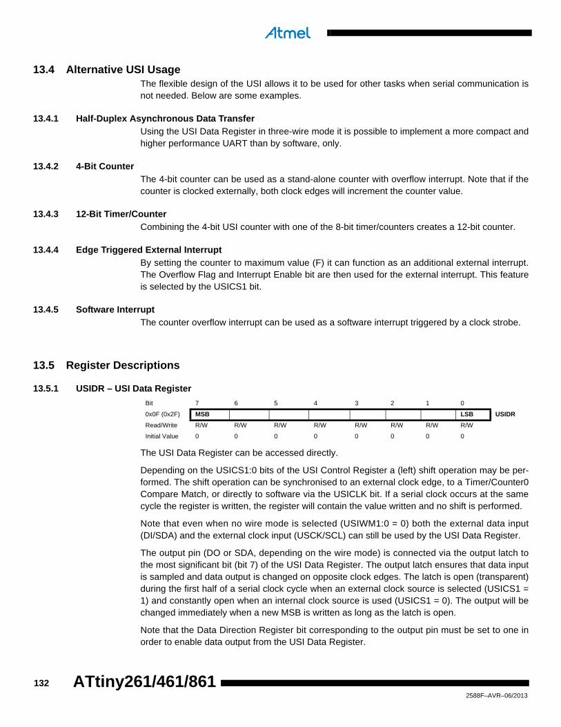
13.4 Alternative USI UsageThe flexible design of the USI allows it to be used for other tasks when serial communication isnot needed. Below are some examples.
13.4.1 Half-Duplex Asynchronous Data Transfer
Using the USI Data Register in three-wire mode it is possible to implement a more compact andhigher performance UART than by software, only.
13.4.2 4-Bit Counter
The 4-bit counter can be used as a stand-alone counter with overflow interrupt. Note that if thecounter is clocked externally, both clock edges will increment the counter value.
13.4.3 12-Bit Timer/Counter
Combining the 4-bit USI counter with one of the 8-bit timer/counters creates a 12-bit counter.
13.4.4 Edge Triggered External Interrupt
By setting the counter to maximum value (F) it can function as an additional external interrupt.The Overflow Flag and Interrupt Enable bit are then used for the external interrupt. This featureis selected by the USICS1 bit.
13.4.5 Software Interrupt
The counter overflow interrupt can be used as a software interrupt triggered by a clock strobe.
13.5 Register Descriptions
13.5.1 USIDR – USI Data Register
The USI Data Register can be accessed directly.
Depending on the USICS1:0 bits of the USI Control Register a (left) shift operation may be per-formed. The shift operation can be synchronised to an external clock edge, to a Timer/Counter0Compare Match, or directly to software via the USICLK bit. If a serial clock occurs at the samecycle the register is written, the register will contain the value written and no shift is performed.
Note that even when no wire mode is selected (USIWM1:0 = 0) both the external data input(DI/SDA) and the external clock input (USCK/SCL) can still be used by the USI Data Register.
The output pin (DO or SDA, depending on the wire mode) is connected via the output latch tothe most significant bit (bit 7) of the USI Data Register. The output latch ensures that data inputis sampled and data output is changed on opposite clock edges. The latch is open (transparent)during the first half of a serial clock cycle when an external clock source is selected (USICS1 =1) and constantly open when an internal clock source is used (USICS1 = 0). The output will bechanged immediately when a new MSB is written as long as the latch is open.
Note that the Data Direction Register bit corresponding to the output pin must be set to one inorder to enable data output from the USI Data Register.
Bit 7 6 5 4 3 2 1 0
0x0F (0x2F) MSB LSB USIDR
Read/Write R/W R/W R/W R/W R/W R/W R/W R/W
Initial Value 0 0 0 0 0 0 0 0
1322588F–AVR–06/2013
ATtiny261/461/861

ATtiny261/461/861
13.5.2 USIBR – USI Buffer Register
The content of the Serial Register is loaded to the USI Buffer Register when the trasfer is com-pleted, and instead of accessing the USI Data Register (the Serial Register) the USI Data Buffercan be accessed when the CPU reads the received data. This gives the CPU time to handleother program tasks too as the controlling of the USI is not so timing critical. The USI flags as setsame as when reading the USIDR register.
13.5.3 USISR – USI Status Register
The Status Register contains Interrupt Flags, line Status Flags and the counter value.
• Bit 7 – USISIF: Start Condition Interrupt Flag
When Two-wire mode is selected, the USISIF Flag is set (to one) when a start condition isdetected. When output disable mode or Three-wire mode is selected and (USICSx = 0b11 &USICLK = 0) or (USICS = 0b10 & USICLK = 0), any edge on the SCK pin sets the flag.
An interrupt will be generated when the flag is set while the USISIE bit in USICR and the GlobalInterrupt Enable Flag are set. The flag will only be cleared by writing a logical one to the USISIFbit. Clearing this bit will release the start detection hold of USCL in Two-wire mode.
A start condition interrupt will wakeup the processor from all sleep modes.
• Bit 6 – USIOIF: Counter Overflow Interrupt Flag
This flag is set (one) when the 4-bit counter overflows (i.e., at the transition from 15 to 0). Aninterrupt will be generated when the flag is set while the USIOIE bit in USICR and the GlobalInterrupt Enable Flag are set. The flag will only be cleared if a one is written to the USIOIF bit.Clearing this bit will release the counter overflow hold of SCL in Two-wire mode.
A counter overflow interrupt will wakeup the processor from Idle sleep mode.
• Bit 5 – USIPF: Stop Condition Flag
When Two-wire mode is selected, the USIPF Flag is set (one) when a stop condition is detected.The flag is cleared by writing a one to this bit. Note that this is not an Interrupt Flag. This signal isuseful when implementing Two-wire bus master arbitration.
• Bit 4 – USIDC: Data Output Collision
This bit is logical one when bit 7 in the USI Data Register differs from the physical pin value. Theflag is only valid when Two-wire mode is used. This signal is useful when implementing Two-wire bus master arbitration.
• Bits 3:0 – USICNT3:0: Counter Value
These bits reflect the current 4-bit counter value. The 4-bit counter value can directly be read orwritten by the CPU.
Bit 7 6 5 4 3 2 1 0
0x10 (0x30) MSB LSB USIBR
Read/Write R R R R R R R R
Initial Value 0 0 0 0 0 0 0 0
Bit 7 6 5 4 3 2 1 0
0x0E (0x2E) USISIF USIOIF USIPF USIDC USICNT3 USICNT2 USICNT1 USICNT0 USISR
Read/Write R/W R/W R/W R R/W R/W R/W R/W
Initial Value 0 0 0 0 0 0 0 0
1332588F–AVR–06/2013

The 4-bit counter increments by one for each clock generated either by the external clock edgedetector, by a Timer/Counter0 Compare Match, or by software using USICLK or USITC strobebits. The clock source depends of the setting of the USICS1:0 bits. For external clock operationa special feature is added that allows the clock to be generated by writing to the USITC strobebit. This feature is enabled by write a one to the USICLK bit while setting an external clocksource (USICS1 = 1).
Note that even when no wire mode is selected (USIWM1:0 = 0) the external clock input(USCK/SCL) are can still be used by the counter.
13.5.4 USICR – USI Control Register
The Control Register includes interrupt enable control, wire mode setting, Clock Select setting,and clock strobe.
• Bit 7 – USISIE: Start Condition Interrupt Enable
Setting this bit to one enables the Start Condition detector interrupt. If there is a pending inter-rupt when the USISIE and the Global Interrupt Enable Flag is set to one, this will immediately beexecuted. Refer to the USISIF bit description on page 133 for further details.
• Bit 6 – USIOIE: Counter Overflow Interrupt Enable
Setting this bit to one enables the Counter Overflow interrupt. If there is a pending interrupt whenthe USIOIE and the Global Interrupt Enable Flag is set to one, this will immediately be executed.Refer to the USIOIF bit description on page 133 for further details.
• Bits 5:4 – USIWM1:0: Wire Mode
These bits set the type of wire mode to be used, as shown in Table 13-1 on page 134.
Basically, only the function of the outputs are affected by these bits. Data and clock inputs arenot affected by the mode selected and will always have the same function. The counter and USIData Register can therefore be clocked externally, and data input sampled, even when outputsare disabled.
Bit 7 6 5 4 3 2 1 0
0x0D (0x2D) USISIE USIOIE USIWM1 USIWM0 USICS1 USICS0 USICLK USITC USICR
Read/Write R/W R/W R/W R/W R/W R/W W W
Initial Value 0 0 0 0 0 0 0 0
Table 13-1. Relationship between USIWM1:0 and USI Operation
USIWM1 USIWM0 Description
0 0Outputs, clock hold, and start detector disabled.
Port pins operate as normal.
0 1
Three-wire mode. Uses DO, DI, and USCK pins.
The Data Output (DO) pin overrides the corresponding bit in the PORTA register. However, the corresponding DDRA bit still controls the data direction. When the port pin is set as input the pin pull-up is controlled by the PORTA bit.
The Data Input (DI) and Serial Clock (USCK) pins do not affect the normal port operation. When operating as master, clock pulses are software generated by toggling the PORTA register, while the data direction is set to output. The USITC bit in the USICR Register can be used for this purpose.
1342588F–AVR–06/2013
ATtiny261/461/861
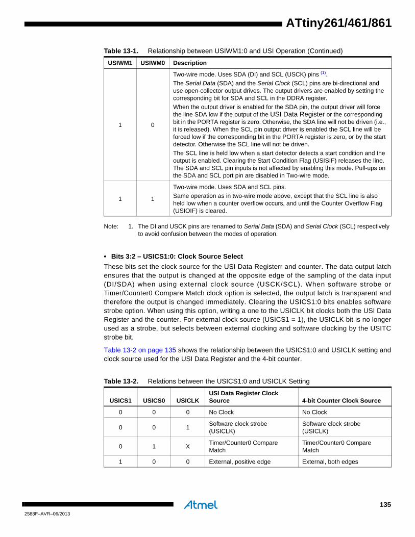
ATtiny261/461/861
Note: 1. The DI and USCK pins are renamed to Serial Data (SDA) and Serial Clock (SCL) respectively to avoid confusion between the modes of operation.
• Bits 3:2 – USICS1:0: Clock Source Select
These bits set the clock source for the USI Data Registerr and counter. The data output latchensures that the output is changed at the opposite edge of the sampling of the data input(DI/SDA) when using external clock source (USCK/SCL). When software strobe orTimer/Counter0 Compare Match clock option is selected, the output latch is transparent andtherefore the output is changed immediately. Clearing the USICS1:0 bits enables softwarestrobe option. When using this option, writing a one to the USICLK bit clocks both the USI DataRegister and the counter. For external clock source (USICS1 = 1), the USICLK bit is no longerused as a strobe, but selects between external clocking and software clocking by the USITCstrobe bit.
Table 13-2 on page 135 shows the relationship between the USICS1:0 and USICLK setting andclock source used for the USI Data Register and the 4-bit counter.
1 0
Two-wire mode. Uses SDA (DI) and SCL (USCK) pins (1).
The Serial Data (SDA) and the Serial Clock (SCL) pins are bi-directional and use open-collector output drives. The output drivers are enabled by setting the corresponding bit for SDA and SCL in the DDRA register.
When the output driver is enabled for the SDA pin, the output driver will force the line SDA low if the output of the USI Data Register or the corresponding bit in the PORTA register is zero. Otherwise, the SDA line will not be driven (i.e., it is released). When the SCL pin output driver is enabled the SCL line will be forced low if the corresponding bit in the PORTA register is zero, or by the start detector. Otherwise the SCL line will not be driven.
The SCL line is held low when a start detector detects a start condition and the output is enabled. Clearing the Start Condition Flag (USISIF) releases the line. The SDA and SCL pin inputs is not affected by enabling this mode. Pull-ups on the SDA and SCL port pin are disabled in Two-wire mode.
1 1
Two-wire mode. Uses SDA and SCL pins.
Same operation as in two-wire mode above, except that the SCL line is also held low when a counter overflow occurs, and until the Counter Overflow Flag (USIOIF) is cleared.
Table 13-2. Relations between the USICS1:0 and USICLK Setting
USICS1 USICS0 USICLKUSI Data Register Clock Source 4-bit Counter Clock Source
0 0 0 No Clock No Clock
0 0 1Software clock strobe (USICLK)
Software clock strobe (USICLK)
0 1 XTimer/Counter0 Compare Match
Timer/Counter0 Compare Match
1 0 0 External, positive edge External, both edges
Table 13-1. Relationship between USIWM1:0 and USI Operation (Continued)
USIWM1 USIWM0 Description
1352588F–AVR–06/2013

• Bit 1 – USICLK: Clock Strobe
Writing a one to this bit location strobes the USI Data Register to shift one step and the counterto increment by one, provided that the USICS1:0 bits are set to zero and by doing so the soft-ware clock strobe option is selected. The output will change immediately when the clock strobeis executed, i.e., in the same instruction cycle. The value shifted into the USI Data Register issampled the previous instruction cycle. The bit will be read as zero.
When an external clock source is selected (USICS1 = 1), the USICLK function is changed froma clock strobe to a Clock Select Register. Setting the USICLK bit in this case will select theUSITC strobe bit as clock source for the 4-bit counter (see Table 13-2).
• Bit 0 – USITC: Toggle Clock Port Pin
Writing a one to this bit location toggles the USCK/SCL value either from 0 to 1, or from 1 to 0.The toggling is independent of the setting in the Data Direction Register, but if the PORT value isto be shown on the pin the DDB2 must be set as output (to one). This feature allows easy clockgeneration when implementing master devices. The bit will be read as zero.
When an external clock source is selected (USICS1 = 1) and the USICLK bit is set to one, writ-ing to the USITC strobe bit will directly clock the 4-bit counter. This allows an early detection ofwhen the transfer is done when operating as a master device.
13.5.5 USIPP – USI Pin Position
• Bits 7:1 – Res: Reserved Bits
These bits are reserved and will always read as zero.
• Bit 0 – USIPOS: USI Pin Position
Setting this bit to one changes the USI pin position. As default pins PB2:PB0 are used for theUSI pin functions, but when writing this bit to one the USIPOS bit is set the USI pin functions areon pins PA2:PA0.
1 1 0 External, negative edge External, both edges
1 0 1 External, positive edge Software clock strobe (USITC)
1 1 1 External, negative edge Software clock strobe (USITC)
Table 13-2. Relations between the USICS1:0 and USICLK Setting (Continued)
USICS1 USICS0 USICLKUSI Data Register Clock Source 4-bit Counter Clock Source
Bit 7 6 5 4 3 2 1 0
0x11 (0x31) - - - - - - - USIPOS USIPP
Read/Write R R R R R R R R/W
Initial Value 0 0 0 0 0 0 0 0
1362588F–AVR–06/2013
ATtiny261/461/861

ATtiny261/461/861
14. AC – Analog ComparatorThe analog comparator compares the input values on the selectable positive pin (AIN0, AIN1 orAIN2) and selectable negative pin (AIN0, AIN1 or AIN2). When the voltage on the positive pin ishigher than the voltage on the negative pin, the Analog Comparator Output, ACO, is set. Thecomparator can trigger a separate interrupt, exclusive to the analog comparator. The user canselect Interrupt triggering on comparator output rise, fall or toggle. A block diagram of the com-parator and its surrounding logic is shown in Figure 14-1.
Figure 14-1. Analog Comparator Block Diagram
Notes: 1. See Table 14-1 on page 137.
See Figure 1-1 on page 2 and Table 10-3 on page 63 for Analog Comparator pin placement.
14.1 Analog Comparator Multiplexed InputWhen the Analog to Digital Converter (ADC) is configurated as single ended input channel, it ispossible to select any of the ADC10:0 pins to replace the negative input to the analog compara-tor. The ADC multiplexer is used to select this input, and consequently, the ADC must beswitched off to utilize this feature. If the Analog Comparator Multiplexer Enable bit (ACME inADCSRB) is set and the ADC is switched off (ADEN in ADCSRA is zero), MUX5:0 in ADMUXselect the input pin to replace the negative input to the analog comparator, as shown in Table14-1. If ACME is cleared or ADEN is set, either AIN0, AIN1 or AIN2 is applied to the negativeinput to the analog comparator.
ACBG
BANDGAPREFERENCE
ADC MULTIPLEXEROUTPUT
ACMEADEN
(1)
MUX
AIN0
AIN1
AIN2
ACM2..1
HS
EL
HLE
V
Table 14-1. Analog Comparator Multiplexed Input
ACME ADEN MUX5:0 ACM2:0 Positive Input Negative Input
0 x xxxxxx 000 AIN0 AIN1
0 x xxxxxx 001 AIN0 AIN2
0 x xxxxxx 010 AIN1 AIN0
0 x xxxxxx 011 AIN1 AIN2
1372588F–AVR–06/2013

0 x xxxxxx 100 AIN2 AIN0
0 x xxxxxx 101,110,111 AIN2 AIN1
1 1 xxxxxx 000 AIN0 AIN1
1 0 000000 000 AIN0 ADC0
1 0 000000 01x AIN1 ADC0
1 0 000000 1xx AIN2 ADC0
1 0 000001 000 AIN0 ADC1
1 0 000001 01x AIN1 ADC1
1 0 000001 1xx AIN2 ADC1
1 0 000010 000 AIN0 ADC2
1 0 000010 01x AIN1 ADC2
1 0 000010 1xx AIN2 ADC2
1 0 000011 000 AIN0 ADC3
1 0 000011 01x AIN1 ADC3
1 0 000011 1xx AIN2 ADC3
1 0 000100 000 AIN0 ADC4
1 0 000100 01x AIN1 ADC4
1 0 000100 1xx AIN2 ADC4
1 0 000101 000 AIN0 ADC5
1 0 000101 01x AIN1 ADC5
1 0 000101 1xx AIN2 ADC5
1 0 000110 000 AIN0 ADC6
1 0 000110 01x AIN1 ADC6
1 0 000110 1xx AIN2 ADC6
1 0 000111 000 AIN0 ADC7
1 0 000111 01x AIN1 ADC7
1 0 000111 1xx AIN2 ADC7
1 0 001000 000 AIN0 ADC8
1 0 001000 01x AIN1 ADC8
1 0 001000 1xx AIN2 ADC8
1 0 001001 000 AIN0 ADC9
1 0 001001 01x AIN1 ADC9
1 0 001001 1xx AIN2 ADC9
1 0 001010 000 AIN0 ADC10
1 0 001010 01x AIN1 ADC10
1 0 001010 1xx AIN2 ADC10
Table 14-1. Analog Comparator Multiplexed Input (Continued)
ACME ADEN MUX5:0 ACM2:0 Positive Input Negative Input
1382588F–AVR–06/2013
ATtiny261/461/861

ATtiny261/461/861
14.2 Register Description
14.2.1 ACSRA – Analog Comparator Control and Status Register A
• Bit 7 – ACD: Analog Comparator Disable
When this bit is written logic one, the power to the analog comparator is switched off. This bitcan be set at any time to turn off the analog comparator, thus reducing power consumption inActive and Idle mode. When changing the ACD bit, the analog comparator Interrupt must be dis-abled by clearing the ACIE bit in ACSRA. Otherwise an interrupt can occur when the bit ischanged.
• Bit 6 – ACBG: Analog Comparator Bandgap Select
When this bit is set an internal 1.1V reference voltage replaces the positive input to the analogcomparator. The selection of the internal voltage reference is done by writing the REFS2:0 bitsin ADCSRB and ADMUX registers. When this bit is cleared, AIN0, AIN1 or AIN2 depending onthe ACM2:0 bits is applied to the positive input of the analog comparator.
• Bit 5 – ACO: Analog Comparator Output
Enables output of analog comparator. The output of the analog comparator is synchronized andthen directly connected to ACO. The synchronization introduces a delay of 1 - 2 clock cycles.
• Bit 4 – ACI: Analog Comparator Interrupt Flag
This bit is set by hardware when a comparator output event triggers the interrupt mode definedby ACIS1 and ACIS0. The analog comparator interrupt routine is executed if the ACIE bit is setand the I-bit in SREG is set. ACI is cleared by hardware when executing the corresponding inter-rupt handling vector. Alternatively, ACI is cleared by writing a logic one to the flag.
• Bit 3 – ACIE: Analog Comparator Interrupt Enable
When the ACIE bit is written logic one and the I-bit in the status register is set, the analog com-parator interrupt is activated. When written logic zero, the interrupt is disabled.
• Bit 2 – ACME: Analog Comparator Multiplexer Enable
When this bit is written logic one and the ADC is switched off (ADEN in ADCSRA is zero), theADC multiplexer selects the negative input to the analog comparator. When this bit is writtenlogic zero, AIN1 is applied to the negative input of the analog comparator. For a detailed descrip-tion of this bit, see Table 14-1 on page 137.
Bit 7 6 5 4 3 2 1 0
0x08 (0x28) ACD ACBG ACO ACI ACIE ACME ACIS1 ACIS0 ACSRA
Read/Write R/W R/W R R/W R/W R/W R/W R/W
Initial Value 0 0 N/A 0 0 0 0 0
1392588F–AVR–06/2013

• Bits 1, 0 – ACIS1, ACIS0: Analog Comparator Interrupt Mode Select
These bits determine which comparator events that trigger the Analog Comparator interrupt. Thedifferent settings are shown in Table 14-2.
When changing the ACIS1/ACIS0 bits, the Analog Comparator Interrupt must be disabled byclearing its Interrupt Enable bit in the ACSR Register. Otherwise an interrupt can occur when thebits are changed.
14.2.2 ACSRB – Analog Comparator Control and Status Register B
• Bit 7 – HSEL: Hysteresis Select
When this bit is written logic one, the hysteresis of the Analog Comparator is switched on. Thehysteresis level is selected by the HLEV bit.
• Bit 6 – HLEV: Hysteresis Level
When the hysteresis is enabled by the HSEL bit, the Hysteresis Level, HLEV, bit selects the hys-teresis level that is either 20mV (HLEV=0) or 50mV (HLEV=1).
• Bits 2:0 – ACM2:ACM0: Analog Comparator Multiplexer
The Analog Comparator multiplexer bits select the positive and negative input pins of the AnalogComparator. The different settings are shown in Table 14-1.
14.2.3 DIDR0 – Digital Input Disable Register 0
• Bits 7:4,2:0 – ADC6D:ADC0D: ADC6:0 Digital Input Disable
When this bit is written logic one, the digital input buffer on the corresponding ADC pin is dis-abled. The corresponding PIN register bit will always read as zero when this bit is set. When ananalog signal is applied to the ADC7:0 pin and the digital input from this pin is not needed, thisbit should be written logic one to reduce power consumption in the digital input buffer.
• Bit 3 – AREFD: AREF Digital Input Disable
When this bit is written logic one, the digital input buffer on the AREF pin is disabled. The corre-sponding PIN register bit will always read as zero when this bit is set. When an analog signal is
Table 14-2. ACIS1/ACIS0 Settings
ACIS1 ACIS0 Interrupt Mode
0 0 Comparator Interrupt on Output Toggle.
0 1 Reserved
1 0 Comparator Interrupt on Falling Output Edge.
1 1 Comparator Interrupt on Rising Output Edge.
Bit 7 6 5 4 3 2 1 0
0x09 (0x29) HSEL HLEV - - - ACM2 ACM1 ACM0 ACSRB
Read/Write R/W R/W R R R R/W R/W R/W
Initial Value 0 0 N/A 0 0 0 0 0
Bit 7 6 5 4 3 2 1 0
0x01 (0x21) ADC6D ADC5D ADC4D ADC3D AREFD ADC2D ADC1D ADC0D DIDR0
Read/Write R/W R/W R/W R/W R/W R/W R/W R/W
Initial Value 0 0 0 0 0 0 0 0
1402588F–AVR–06/2013
ATtiny261/461/861

ATtiny261/461/861
applied to the AREF pin and the digital input from this pin is not needed, this bit should be writtenlogic one to reduce power consumption in the digital input buffer.
14.2.4 DIDR1 – Digital Input Disable Register 1
• Bits 7:4 – ADC10D:ADC7D: ADC10:7 Digital Input Disable
When this bit is written logic one, the digital input buffer on the corresponding ADC pin is dis-abled. The corresponding PIN register bit will always read as zero when this bit is set. When ananalog signal is applied to the ADC10:7 pin and the digital input from this pin is not needed, thisbit should be written logic one to reduce power consumption in the digital input buffer.
Bit 7 6 5 4 3 2 1 0
0x02 (0x22) ADC10D ADC9D ADC8D ADC7D - DIDR1
Read/Write R/W R/W R/W R/W R R R R
Initial Value 0 0 0 0 0 0 0 0
1412588F–AVR–06/2013

15. ADC – Analog to Digital Converter
15.1 Features• 10-bit Resolution
• 1.0 LSB Integral Non-linearity
• ± 2 LSB Absolute Accuracy
• 13µs Conversion Time
• 15 kSPS at Maximum Resolution
• 11 Multiplexed Single Ended Input Channels
• 16 Differential input pairs
• 15 Differential input pairs with selectable gain
• Temperature Sensor Input Channel
• Optional Left Adjustment for ADC Result Readout
• 0 - VCC ADC Input Voltage Range
• Selectable 1.1V / 2.56V ADC Voltage Reference
• Free Running or Single Conversion Mode
• ADC Start Conversion by Auto Triggering on Interrupt Sources
• Interrupt on ADC Conversion Complete
• Sleep Mode Noise Cancele
• Unipolar / Bipolar Input Mode
• Input Polarity Reversal Mode
15.2 OverviewThe ATtiny261/461/861 features a 10-bit successive approximation ADC. The ADC is connectedto a 11-channel Analog Multiplexer which allows 16 differential voltage input combinations and11 single-ended voltage inputs constructed from the pins PA7:PA0 or PB7:PB4. The differentialinput is equipped with a programmable gain stage, providing amplification steps of 1x, 8x, 20x or32x on the differential input voltage before the A/D conversion. The single-ended voltage inputsrefer to 0V (GND).
The ADC contains a Sample and Hold circuit which ensures that the input voltage to the ADC isheld at a constant level during conversion. A block diagram of the ADC is shown in Figure 15-1on page 143.
Internal reference voltages of nominally 1.1V or 2.56V are provided On-chip. The Internal refer-ance voltage of 2.56V, can optionally be externally decoupled at the AREF (PA3) pin by acapacitor, for better noise performance. Alternatively, VCC can be used as reference voltage forsingle ended channels. There is also an option to use an external voltage reference and turn-offthe internal voltage reference. These options are selected using the REFS2:0 bits of the ADC-SRB and ADMUX registers.
1422588F–AVR–06/2013
ATtiny261/461/861

ATtiny261/461/861
Figure 15-1. Analog to Digital Converter Block Schematic
15.3 OperationThe ADC converts an analog input voltage to a 10-bit digital value through successive approxi-mation. The minimum value represents GND and the maximum value represents the voltage onVCC, the voltage on the AREF pin or an internal 1.1V / 2.56V voltage reference.
The voltage reference for the ADC may be selected by writing to the REFS2:0 bits in ADCSRBand ADMUX registers. The VCC supply, the AREF pin or an internal 1.1V / 2.56V voltage refer-ence may be selected as the ADC voltage reference. Optionally the internal 1.1V / 2.56V voltage
ADC CONVERSIONCOMPLETE IRQ
8-BIT DATA BUS
15 0
ADC MULTIPLEXERSELECT (ADMUX)
ADC CTRL. & STATUSREGISTER A (ADCSRA)
ADC DATA REGISTER(ADCH/ADCL)
MU
X2
AD
IE
AD
ATE
AD
SC
AD
EN
AD
IFA
DIF
MU
X1
MU
X0
AD
PS0
AD
PS1
AD
PS2
MU
X3
CONVERSION LOGIC
10-BIT DAC
+-
SAMPLE & HOLDCOMPARATOR
MUX DECODER
MU
X4
ADC7
ADC6
ADC5
ADC4
ADC3
ADC2
ADC1
ADC0
REFS
0
REFS
1
AD
LAR
+
-
CHA
NN
EL S
ELEC
TIO
N
GA
IN S
ELEC
TIO
N
AD
C[9:
0]
ADCMULTIPLEXER OUTPUT
GAINAMPLIFIER
INTERNAL 1.1VREFERENCE
PRESCALER
SINGLE ENDED / DIFFERENTIAL SELECTION
AGND
POS.INPUTMUX
NEG.INPUTMUX
ADC10
ADC9
ADC8
VCC
AREF
TEMPERATURESENSOR
INTERNAL 2.56/1.1VREFERENCE
MUX
ADC CTRL. & STATUSREGISTER B (ADCSRB)
REFS
2
GSE
L
MU
X5
1432588F–AVR–06/2013

reference may be decoupled by an external capacitor at the AREF pin to improve noiseimmunity.
The analog input channel and differential gain are selected by writing to the MUX5:0 bits inADMUX. Any of the 11 ADC input pins ADC10:0 can be selected as single ended inputs to theADC. The positive and negative inputs to the differential gain amplifier are described in Table15-4.
If differential channels are selected, the differential gain stage amplifies the voltage differencebetween the selected input pair by the selected gain factor, 1x, 8x, 20x or 32x, according to thesetting of the MUX5:0 bits in ADMUX and the GSEL bit in ADCSRB. This amplified value thenbecomes the analog input to the ADC. If single ended channels are used, the gain amplifier isbypassed altogether.
If the same ADC input pin is selected as both the positive and negative input to the differentialgain amplifier, the remaining offset in the gain stage and conversion circuitry can be measureddirectly as the result of the conversion. This figure can be subtracted from subsequent conver-sions with the same gain setting to reduce offset error to below 1 LSW.
The on-chip temperature sensor is selected by writing the code “111111” to the MUX5:0 bits inADMUX register when the ADC11 channel is used as an ADC input.
The ADC is enabled by setting the ADC Enable bit, ADEN in ADCSRA. Voltage reference andinput channel selections will not go into effect until ADEN is set. The ADC does not consumepower when ADEN is cleared, so it is recommended to switch off the ADC before entering powersaving sleep modes.
The ADC generates a 10-bit result which is presented in the ADC Data Registers, ADCH andADCL. By default, the result is presented right adjusted, but can optionally be presented leftadjusted by setting the ADLAR bit in ADMUX.
If the result is left adjusted and no more than 8-bit precision is required, it is sufficient to readADCH. Otherwise, ADCL must be read first, then ADCH, to ensure that the content of the dataregisters belongs to the same conversion. Once ADCL is read, ADC access to data registers isblocked. This means that if ADCL has been read, and a conversion completes before ADCH isread, neither register is updated and the result from the conversion is lost. When ADCH is read,ADC access to the ADCH and ADCL Registers is re-enabled.
The ADC has its own interrupt which can be triggered when a conversion completes. When ADCaccess to the data registers is prohibited between reading of ADCH and ADCL, the interrupt willtrigger even if the result is lost.
15.4 Starting a ConversionA single conversion is started by writing a logical one to the ADC Start Conversion bit, ADSC.This bit stays high as long as the conversion is in progress and will be cleared by hardwarewhen the conversion is completed. If a different data channel is selected while a conversion is inprogress, the ADC will finish the current conversion before performing the channel change.
Alternatively, a conversion can be triggered automatically by various sources. Auto Triggering isenabled by setting the ADC Auto Trigger Enable bit, ADATE in ADCSRA. The trigger source isselected by setting the ADC Trigger Select bits, ADTS in ADCSRB (see description of the ADTSbits for a list of the trigger sources). When a positive edge occurs on the selected trigger signal,the ADC prescaler is reset and a conversion is started. This provides a method of starting con-versions at fixed intervals. If the trigger signal still is set when the conversion completes, a new
1442588F–AVR–06/2013
ATtiny261/461/861

ATtiny261/461/861
conversion will not be started. If another positive edge occurs on the trigger signal during con-version, the edge will be ignored. Note that an Interrupt Flag will be set even if the specificinterrupt is disabled or the Global Interrupt Enable bit in SREG is cleared. A conversion can thusbe triggered without causing an interrupt. However, the Interrupt Flag must be cleared in order totrigger a new conversion at the next interrupt event.
Figure 15-2. ADC Auto Trigger Logic
Using the ADC Interrupt Flag as a trigger source makes the ADC start a new conversion as soonas the ongoing conversion has finished. The ADC then operates in Free Running mode, con-stantly sampling and updating the ADC Data Register. The first conversion must be started bywriting a logical one to the ADSC bit in ADCSRA. In this mode the ADC will perform successiveconversions independently of whether the ADC Interrupt Flag, ADIF is cleared or not.
If Auto Triggering is enabled, single conversions can be started by writing ADSC in ADCSRA toone. ADSC can also be used to determine if a conversion is in progress. The ADSC bit will beread as one during a conversion, independently of how the conversion was started.
15.5 Prescaling and Conversion TimingBy default, the successive approximation circuitry requires an input clock frequency between 50kHz and 200 kHz to get maximum resolution. If a lower resolution than 10 bits is needed, theinput clock frequency to the ADC can be higher than 200 kHz to get a higher sample rate.
The ADC module contains a prescaler, which generates an acceptable ADC clock frequencyfrom any CPU frequency above 100 kHz. The prescaling is set by the ADPS bits in ADCSRA.The prescaler starts counting from the moment the ADC is switched on by setting the ADEN bitin ADCSRA. The prescaler keeps running for as long as the ADEN bit is set, and is continuouslyreset when ADEN is low.
See Figure 15-3 on page 146.
ADSC
ADIF
SOURCE 1
SOURCE n
ADTS[2:0]
CONVERSIONLOGIC
PRESCALER
START CLKADC
.
.
.
. EDGEDETECTOR
ADATE
1452588F–AVR–06/2013

Figure 15-3. ADC Prescaler
When initiating a single ended conversion by setting the ADSC bit in ADCSRA, the conversionstarts at the following rising edge of the ADC clock cycle.
A normal conversion takes 13 ADC clock cycles. The first conversion after the ADC is switchedon (ADEN in ADCSRA is set) takes 25 ADC clock cycles in order to initialize the analog circuitry,as shown in Figure 15-4 below.
Figure 15-4. ADC Timing Diagram, First Conversion (Single Conversion Mode)
The actual sample-and-hold takes place 1.5 ADC clock cycles after the start of a normal conver-sion and 13.5 ADC clock cycles after the start of an first conversion. See Figure 15-5. When aconversion is complete, the result is written to the ADC Data Registers, and ADIF is set. In Sin-gle Conversion mode, ADSC is cleared simultaneously. The software may then set ADSC again,and a new conversion will be initiated on the first rising ADC clock edge.
7-BIT ADC PRESCALER
ADC CLOCK SOURCE
CK
ADPS0ADPS1ADPS2
CK
/128
CK
/2
CK
/4
CK
/8
CK
/16
CK
/32
CK
/64
ResetADENSTART
Sign and MSB of Result
LSB of Result
ADC Clock
ADSC
Sample & Hold
ADIF
ADCH
ADCL
Cycle Number
ADEN
1 2 12 13 14 15 16 17 18 19 20 21 22 23 24 25 1 2
First ConversionNextConversion
3
MUX and REFSUpdate
MUX and REFSUpdate
ConversionComplete
1462588F–AVR–06/2013
ATtiny261/461/861

ATtiny261/461/861
Figure 15-5. ADC Timing Diagram, Single Conversion
When Auto Triggering is used, the prescaler is reset when the trigger event occurs. See Figure15-6. This assures a fixed delay from the trigger event to the start of conversion. In this mode,the sample-and-hold takes place two ADC clock cycles after the rising edge on the triggersource signal. Three additional CPU clock cycles are used for synchronization logic.
Figure 15-6. ADC Timing Diagram, Auto Triggered Conversion
In Free Running mode (see Figure 15-7), a new conversion will be started immediately after theconversion completes, while ADSC remains high.
1 2 3 4 5 6 7 8 9 10 11 12 13
Sign and MSB of Result
LSB of Result
ADC Clock
ADSC
ADIF
ADCH
ADCL
Cycle Number 1 2
One Conversion Next Conversion
3
Sample & Hold
MUX and REFSUpdate
ConversionComplete
MUX and REFSUpdate
1 2 3 4 5 6 7 8 9 10 11 12 13
Sign and MSB of Result
LSB of Result
ADC Clock
TriggerSource
ADIF
ADCH
ADCL
Cycle Number 1 2
One Conversion Next Conversion
ConversionCompletePrescaler
Reset
ADATE
PrescalerReset
Sample &Hold
MUX and REFS Update
1472588F–AVR–06/2013

Figure 15-7. ADC Timing Diagram, Free Running Conversion
For a summary of conversion times, see Table 15-1.
15.6 Changing Channel or Reference SelectionThe MUX5:0 and REFS2:0 bits in the ADCSRB and ADMUX registers are single bufferedthrough a temporary register to which the CPU has random access. This ensures that the chan-nels and reference selection only takes place at a safe point during the conversion. The channeland reference selection is continuously updated until a conversion is started. Once the conver-sion starts, the channel and reference selection is locked to ensure a sufficient sampling time forthe ADC. Continuous updating resumes in the last ADC clock cycle before the conversion com-pletes (ADIF in ADCSRA is set). Note that the conversion starts on the following rising ADCclock edge after ADSC is written. The user is thus advised not to write new channel or referenceselection values to ADMUX until one ADC clock cycle after ADSC is written.
If Auto Triggering is used, the exact time of the triggering event can be indeterministic. Specialcare must be taken when updating the ADMUX Register, in order to control which conversionwill be affected by the new settings.
If both ADATE and ADEN is written to one, an interrupt event can occur at any time. If theADMUX Register is changed in this period, the user cannot tell if the next conversion is basedon the old or the new settings.
ADMUX can be safely updated in the following ways:
Table 15-1. ADC Conversion Time
ConditionSample & Hold (Cycles from Start of Conversion) Total Conversion Time (Cycles)
First conversion 13.5 25
Normal conversions 1.5 13
Auto Triggered conversions 2 13.5
11 12 13
Sign and MSB of Result
LSB of Result
ADC Clock
ADSC
ADIF
ADCH
ADCL
Cycle Number1 2
One Conversion Next Conversion
3 4
ConversionComplete
Sample & Hold
MUX and REFSUpdate
1482588F–AVR–06/2013
ATtiny261/461/861

ATtiny261/461/861
• When ADATE or ADEN is cleared.
• During conversion, minimum one ADC clock cycle after the trigger event.
• After a conversion, before the Interrupt Flag used as trigger source is cleared.
When updating ADMUX in one of these conditions, the new settings will affect the next ADCconversion.
15.6.1 ADC Input Channels
When changing channel selections, the user should observe the following guidelines to ensurethat the correct channel is selected:
In Single Conversion mode, always select the channel before starting the conversion. The chan-nel selection may be changed one ADC clock cycle after writing one to ADSC. However, thesimplest method is to wait for the conversion to complete before changing the channel selection.
In Free Running mode, always select the channel before starting the first conversion. The chan-nel selection may be changed one ADC clock cycle after writing one to ADSC. However, thesimplest method is to wait for the first conversion to complete, and then change the channelselection. Since the next conversion has already started automatically, the next result will reflectthe previous channel selection. Subsequent conversions will reflect the new channel selection.
15.6.2 ADC Voltage Reference
The voltage reference for the ADC (VREF) indicates the conversion range for the ADC. Singleended channels that exceed VREF will result in codes close to 0x3FF. VREF can be selected aseither VCC, or internal 1.1V / 2.56V voltage reference, or external AREF pin. The first ADC con-version result after switching voltage reference source may be inaccurate, and the user isadvised to discard this result.
15.7 ADC Noise CancelerThe ADC features a noise canceler that enables conversion during sleep mode. This reducesnoise induced from the CPU core and other I/O peripherals. The noise canceler can be usedwith ADC Noise Reduction and Idle mode. To make use of this feature, the following procedureshould be used:
• Make sure that the ADC is enabled and is not busy converting. Single Conversion mode must be selected and the ADC conversion complete interrupt must be enabled.
• Enter ADC Noise Reduction mode (or Idle mode). The ADC will start a conversion once the CPU has been halted.
• If no other interrupts occur before the ADC conversion completes, the ADC interrupt will wake up the CPU and execute the ADC Conversion Complete interrupt routine. If another interrupt wakes up the CPU before the ADC conversion is complete, that interrupt will be executed, and an ADC Conversion Complete interrupt request will be generated when the ADC conversion completes. The CPU will remain in active mode until a new sleep command is executed.
Note that the ADC will not automatically be turned off when entering other sleep modes than Idlemode and ADC Noise Reduction mode. The user is advised to write zero to ADEN before enter-ing such sleep modes to avoid excessive power consumption.
1492588F–AVR–06/2013

15.8 Analog Input CircuitryThe analog input circuitry for single ended channels is illustrated in Figure 15-8 An analogsource applied to ADCn is subjected to the pin capacitance and input leakage of that pin, regard-less of whether that channel is selected as input for the ADC. When the channel is selected, thesource must drive the S/H capacitor through the series resistance (combined resistance in theinput path).
Figure 15-8. Analog Input Circuitry
The capacitor in Figure 15-8 depicts the total capacitance, including the sample/hold capacitorand any stray or parasitic capacitance inside the device. The value given is worst case.
The ADC is optimized for analog signals with an output impedance of approximately 10 k orless. If such a source is used, the sampling time will be negligible. If a source with higher imped-ance is used, the sampling time will depend on how long time the source needs to charge theS/H capacitor, with can vary widely. The user is recommended to only use low impedant sourceswith slowly varying signals, since this minimizes the required charge transfer to the S/Hcapacitor.
Signal components higher than the Nyquist frequency (fADC/2) should not be present to avoiddistortion from unpredictable signal convolution. The user is advised to remove high frequencycomponents with a low-pass filter before applying the signals as inputs to the ADC.
15.9 Noise Canceling TechniquesDigital circuitry inside and outside the device generates EMI which might affect the accuracy ofanalog measurements. When conversion accuracy is critical, the noise level can be reduced byapplying the following techniques:
• Keep analog signal paths as short as possible.
• Make sure analog tracks run over the analog ground plane.
• Keep analog tracks well away from high-speed switching digital tracks.
• If any port pin is used as a digital output, it mustn’t switch while a conversion is in progress.
• Place bypass capacitors as close to VCC and GND pins as possible.
Where high ADC accuracy is required it is recommended to use ADC Noise Reduction Mode, asdescribed in Section 15.7 on page 149. This is especially the case when system clock frequencyis above 1 MHz, or when the ADC is used for reading the internal temperature sensor, as
ADCn
IIH
1..100 kΩCS/H= 14 pF
VCC/2
IIL
1502588F–AVR–06/2013
ATtiny261/461/861

ATtiny261/461/861
described in Section 15.12 on page 154. A good system design with properly placed, externalbypass capacitors does reduce the need for using ADC Noise Reduction Mode
15.10 ADC Accuracy DefinitionsAn n-bit single-ended ADC converts a voltage linearly between GND and VREF in 2n steps(LSBs). The lowest code is read as 0, and the highest code is read as 2n-1.
Several parameters describe the deviation from the ideal behavior:
• Offset: The deviation of the first transition (0x000 to 0x001) compared to the ideal transition (at 0.5 LSB). Ideal value: 0 LSB.
Figure 15-9. Offset Error
Output Code
VREF Input Voltage
Ideal ADC
Actual ADC
OffsetError
1512588F–AVR–06/2013

• Gain Error: After adjusting for offset, the Gain Error is found as the deviation of the last transition (0x3FE to 0x3FF) compared to the ideal transition (at 1.5 LSB below maximum). Ideal value: 0 LSB
Figure 15-10. Gain Error
• Integral Non-linearity (INL): After adjusting for offset and gain error, the INL is the maximum deviation of an actual transition compared to an ideal transition for any code. Ideal value: 0 LSB.
Figure 15-11. Integral Non-linearity (INL)
Output Code
VREF Input Voltage
Ideal ADC
Actual ADC
GainError
Output Code
VREF Input Voltage
Ideal ADC
Actual ADC
INL
1522588F–AVR–06/2013
ATtiny261/461/861

ATtiny261/461/861
• Differential Non-linearity (DNL): The maximum deviation of the actual code width (the interval between two adjacent transitions) from the ideal code width (1 LSB). Ideal value: 0 LSB.
Figure 15-12. Differential Non-linearity (DNL)
• Quantization Error: Due to the quantization of the input voltage into a finite number of codes, a range of input voltages (1 LSB wide) will code to the same value. Always ± 0.5 LSB.
• Absolute Accuracy: The maximum deviation of an actual (unadjusted) transition compared to an ideal transition for any code. This is the compound effect of offset, gain error, differential error, non-linearity, and quantization error. Ideal value: ± 0.5 LSB.
15.11 ADC Conversion ResultAfter the conversion is complete (ADIF is high), the conversion result can be found in the ADCResult Registers (ADCL, ADCH). The form of the conversion result depends on the type of theconversio as there are three types of conversions: single ended conversion, unipolar differentialconversion and bipolar differential conversion.
15.11.1 Single Ended Conversion
For single ended conversion, the result is
where VIN is the voltage on the selected input pin and VREF the selected voltage reference (seeTable 15-3 on page 155 and Table 15-4 on page 157). 0x000 represents analog ground, and
Output Code
0x3FF
0x000
0 VREF Input Voltage
DNL
1 LSB
ADCVIN 1024
VREF--------------------------=
1532588F–AVR–06/2013

0x3FF represents the selected voltage reference minus one LSB. The result is presented in one-sided form, from 0x3FF to 0x000.
15.11.2 Unipolar Differential Conversion
If differential channels and an unipolar input mode are used, the result is
where VPOS is the voltage on the positive input pin, VNEG the voltage on the negative input pin,and VREF the selected voltage reference (see Table 15-3 on page 155 and Table 15-4 on page157). The voltage on the positive pin must always be larger than the voltage on the negative pinor otherwise the voltage difference is saturated to zero. The result is presented in one-sidedform, from 0x000 (0d) to 0x3FF (+1023d). The GAIN is either 1x, 8x, 20x or 32x.
15.11.3 Bipolar Differential Conversion
As default the ADC converter operates in the unipolar input mode, but the bipolar input modecan be selected by writting the BIN bit in the ADCSRB to one. In the bipolar input mode two-sided voltage differences are allowed and thus the voltage on the negative input pin can also belarger than the voltage on the positive input pin. If differential channels and a bipolar input modeare used, the result is
where VPOS is the voltage on the positive input pin, VNEG the voltage on the negative input pin,and VREF the selected voltage reference. The result is presented in two’s complement form, from0x200 (-512d) through 0x000 (+0d) to 0x1FF (+511d). The GAIN is either 1x, 8x, 20x or 32x.
However, if the signal is not bipolar by nature (9 bits + sign as the 10th bit), this scheme losesone bit of the converter dynamic range. Then, if the user wants to perform the conversion withthe maximum dynamic range, the user can perform a quick polarity check of the result and usethe unipolar differential conversion with selectable differential input pair. When the polarity checkis performed, it is sufficient to read the MSB of the result (ADC9 in ADCH). If the bit is one, theresult is negative, and if this bit is zero, the result is positive.
15.12 Temperature MeasurementThe temperature measurement is based on an on-chip temperature sensor that is coupled to asingle ended ADC11 channel. Selecting the ADC11 channel by writing the MUX5:0 bits inADMUX register to “111111” enables the temperature sensor. The internal 1.1V voltage refer-ence must also be selected for the ADC voltage reference source in the temperature sensormeasurement. When the temperature sensor is enabled, the ADC converter can be used in sin-gle conversion mode to measure the voltage over the temperature sensor.
The measured voltage has a linear relationship to the temperature as described in Table 15-2The sensitivity is approximately 1 LSB / C and the accuracy depends on the method of user cal-ibration. Typically, the measurement accuracy after a single temperature calibration is ±10C,
ADCVPOS VNEG– 1024
VREF-------------------------------------------------------- GAIN=
ADCVPOS VNEG– 512
VREF----------------------------------------------------- GAIN=
1542588F–AVR–06/2013
ATtiny261/461/861

ATtiny261/461/861
assuming calibration at room temperature. Better accuracies are achieved by using twotemperature points for calibration.
The values described in Table 15-2 are typical values. However, due to process variation thetemperature sensor output voltage varies from one chip to another. To be capable of achievingmore accurate results the temperature measurement can be calibrated in the application soft-ware. The sofware calibration can be done using the formula:
T = k * [(ADCH << 8) | ADCL] + TOS
where ADCH and ADCL are the ADC data registers, k is the fixed slope coefficient and TOS isthe temperature sensor offset. Typically, k is very close to 1.0 and in single-point calibration thecoefficient may be omitted. Where higher accuracy is required the slope coefficient should beevaluated based on measurements at two temperatures.
15.13 Register Description
15.13.1 ADMUX – ADC Multiplexer Selection Register
• Bits 7:6 – REFS1:REFS0: Voltage Reference Selection Bits
These bits together with the REFS2 bit from the ADC Control and Status Register B (ADCSRB)select the voltage reference for the ADC, as shown in Table 15-3.
If these bits are changed during a conversion, the change will not go in effect until this conver-sion is complete (ADIF in ADCSR is set). Also note, that when these bits are changed, the nextconversion will take 25 ADC clock cycles.
Table 15-2. Temperature vs. Sensor Output Voltage (Typical Case)
Temperature -40 C +25 C +85 C
ADC 230 LSB 300 LSB 370 LSB
Bit 7 6 5 4 3 2 1 0
0x07 (0x27) REFS1 REFS0 ADLAR MUX4 MUX3 MUX2 MUX1 MUX0 ADMUX
Read/Write R/W R/W R/W R/W R/W R/W R/W R/W
Initial Value 0 0 0 0 0 0 0 0
Table 15-3. Voltage Reference Selections for ADC
REFS2 REFS1 REFS0 Voltage Reference Selection
X 0 0VCC used as voltage reference,disconnected from AREF
X 0 1External voltage reference at AREF pin,internal voltage reference turned off
0 1 0 Internal 1.1V voltage reference
0 1 1 Reserved
1 1 0Internal 2.56V voltage reference,without external bypass capacitor,disconnected from AREF
1 1 1Internal 2.56V voltage reference,with external bypass capacitor at AREF pin
1552588F–AVR–06/2013

Special care should be taken when changing differential channels. Once a differential channelhas been selected the input stage may take a while to stabilize. It is therefore recommended toforce the ADC to perform a long conversion when changing multiplexer or voltage reference set-tings. This can be done by first turning off the ADC, then changing reference settings and thenturn on the ADC. Alternatively, the first conversion results after changing reference settingsshould be discarded.
It is not recommended to use an external AREF higher than (VCC - 1V) for channels with differ-ential gain, as this will affect ADC accuracy.
Internal voltage reference options may not be used if an external voltage is being applied to theAREF pin.
• Bit 5 – ADLAR: ADC Left Adjust Result
The ADLAR bit affects the presentation of the ADC conversion result in the ADC Data Register.Write one to ADLAR to left adjust the result. Otherwise, the result is right adjusted. Changing theADLAR bit will affect the ADC Data Register immediately, regardless of any ongoing conver-sions. For a comple te description of this bit, see “ADCL and ADCH – The ADC Data Register”on page 160.
• Bits 4:0 – MUX4:0: Analog Channel and Gain Selection Bits
These bits and the MUX5 bit from the ADC Control and Status Register B (ADCSRB) selectwhich combination of analog inputs are connected to the ADC. In case of differential input, gainselection is also made with these bits. Selecting the same pin as both inputs to the differential
1562588F–AVR–06/2013
ATtiny261/461/861

ATtiny261/461/861
gain stage enables offset measurements. Selecting the single-ended channel ADC11 enablesthe temperature sensor. Refer to Table 15-4 for details.
Table 15-4. Input Channel Selections
MUX5:0Single-Ended
Input
Differential Input
GainPositive Negative
000000 ADC0 (PA0)
NA NA NA
000001 ADC1 (PA1)
000010 ADC2 (PA2)
000011 ADC3 (PA4)
000100 ADC4 (PA5)
000101 ADC5 (PA6)
000110 ADC6 (PA7)
000111 ADC7 (PB4)
001000 ADC8 (PB5)
001001 ADC9 (PB6)
001010 ADC10 (PB7)
001011
NA
ADC0 (PA0) ADC1 (PA1) 20x
001100 ADC0 (PA0) ADC1 (PA1) 1x
001101 ADC1 (PA1) ADC1 (PA1) 20x
001110 ADC2 (PA2) ADC1 (PA1) 20x
001111 ADC2 (PA2) ADC1 (PA1) 1x
010000
N/A
ADC2 (PA2) ADC3 (PA4) 1x
010001 ADC3 (PA4) ADC3 (PA4) 20x
010010 ADC4 (PA5) ADC3 (PA4) 20x
010011 ADC4 (PA5) ADC3 (PA4) 1x
010100
NA
ADC4 (PA5) ADC5 (PA6) 20x
010101 ADC4 (PA5) ADC5 (PA6) 1x
010110 ADC5 (PA6) ADC5 (PA6) 20x
010111 ADC6 (PA7) ADC5 (PA6) 20x
011000 ADC6 (PA7) ADC5 (PA6) 1x
011001
NA
ADC8 (PB5) ADC9 (PB6) 20x
011010 ADC8 (PB5) ADC9 (PB6) 1x
011011 ADC9 (PB6) ADC9 (PB6) 20x
011100 ADC10 (PB7) ADC9 (PB6) 20x
011101 ADC10 (PB7) ADC9 (PB6) 1x
011110 1.1VN/A N/A N/A
011111 0V
1572588F–AVR–06/2013

Note: 1. Temperature sensor
100000
N/A
ADC0(PA0) ADC1(PA1) 20x/32x
100001 ADC0(PA0) ADC1(PA1) 1x/8x
100010 ADC1(PA1 ADC0(PA0) 20x/32x
100011 ADC1(PA1) ADC0(PA0) 1x/8x
100100
N/A
ADC1(PA1) ADC2(PA2) 20x/32x
100101 ADC1(PA1) ADC2(PA2) 1x/8x
100110 ADC2(PA2 ADC1(PA1) 20x/32x
100111 ADC2(PA2) ADC1(PA1) 1x/8x
101000
N/A
ADC2(PA2) ADC0(PA0) 20x/32x
101001 ADC2(PA2) ADC0(PA0) 1x/8x
101010 ADC0(PA0) ADC2(PA2) 20x/32x
101011 ADC0(PA0) ADC2(PA2) 1x/8x
101100
N/A
ADC4(PA5) ADC5(PA6) 20x/32x
101101 ADC4(PA5) ADC5(PA6) 1x/8x
101110 ADC5(PA6) ADC4(PA5) 20x/32x
101111 ADC5(PA6) ADC4(PA5) 1x/8x
110000
N/A
ADC5(PA6) ADC6(PA7) 20x/32x
110001 ADC5(PA6) ADC6(PA7) 1x/8x
110010 ADC6(PA7) ADC5(PA6) 20x/32x
110011 ADC6(PA7) ADC5(PA6) 1x/8x
110100
N/A
ADC6(PA7) ADC4(PA5) 20x/32x
110101 ADC6(PA7) ADC4(PA5) 1x/8x
110110 ADC4(PA5) ADC6(PA7) 20x/32x
110111 ADC4(PA5) ADC6(PA7) 1x/8x
111000
N/A
ADC0(PA0) ADC0(PA0) 20x/32x
111001 ADC0(PA0) ADC0(PA0) 1x/8x
111010 ADC1(PA1) ADC1(PA1) 20x/32x
111011 ADC2(PA2) ADC2(PA2) 20x/32x
111100
N/A
ADC4(PA5) ADC4(PA5) 20x/32x
111101 ADC5(PA6) ADC5(PA6) 20x/32x
111110 ADC6(PA7) ADC6(PA7) 20x/32x
111111 ADC11 (1) N/A N/A N/A
Table 15-4. Input Channel Selections (Continued)
MUX5:0Single-Ended
Input
Differential Input
GainPositive Negative
1582588F–AVR–06/2013
ATtiny261/461/861
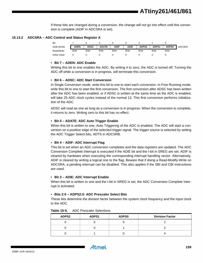
ATtiny261/461/861
If these bits are changed during a conversion, the change will not go into effect until this conver-sion is complete (ADIF in ADCSRA is set).
15.13.2 ADCSRA – ADC Control and Status Register A
• Bit 7 – ADEN: ADC Enable
Writing this bit to one enables the ADC. By writing it to zero, the ADC is turned off. Turning theADC off while a conversion is in progress, will terminate this conversion.
• Bit 6 – ADSC: ADC Start Conversion
In Single Conversion mode, write this bit to one to start each conversion. In Free Running mode,write this bit to one to start the first conversion. The first conversion after ADSC has been writtenafter the ADC has been enabled, or if ADSC is written at the same time as the ADC is enabled,will take 25 ADC clock cycles instead of the normal 13. This first conversion performs initializa-tion of the ADC.
ADSC will read as one as long as a conversion is in progress. When the conversion is complete,it returns to zero. Writing zero to this bit has no effect.
• Bit 5 – ADATE: ADC Auto Trigger Enable
When this bit is written to one, Auto Triggering of the ADC is enabled. The ADC will start a con-version on a positive edge of the selected trigger signal. The trigger source is selected by settingthe ADC Trigger Select bits, ADTS in ADCSRB.
• Bit 4 – ADIF: ADC Interrupt Flag
This bit is set when an ADC conversion completes and the data registers are updated. The ADCConversion Complete Interrupt is executed if the ADIE bit and the I-bit in SREG are set. ADIF iscleared by hardware when executing the corresponding interrupt handling vector. Alternatively,ADIF is cleared by writing a logical one to the flag. Beware that if doing a Read-Modify-Write onADCSRA, a pending interrupt can be disabled. This also applies if the SBI and CBI instructionsare used.
• Bit 3 – ADIE: ADC Interrupt Enable
When this bit is written to one and the I-bit in SREG is set, the ADC Conversion Complete Inter-rupt is activated.
• Bits 2:0 – ADPS2:0: ADC Prescaler Select Bits
These bits determine the division factor between the system clock frequency and the input clockto the ADC.
Bit 7 6 5 4 3 2 1 0
0x06 (0x26) ADEN ADSC ADATE ADIF ADIE ADPS2 ADPS1 ADPS0 ADCSRA
Read/Write R/W R/W R/W R/W R/W R/W R/W R/W
Initial Value 0 0 0 0 0 0 0 0
Table 15-5. ADC Prescaler Selections
ADPS2 ADPS1 ADPS0 Division Factor
0 0 0 2
0 0 1 2
0 1 0 4
1592588F–AVR–06/2013

15.13.3 ADCL and ADCH – The ADC Data Register
15.13.3.1 ADLAR = 0
15.13.3.2 ADLAR = 1
When an ADC conversion is complete, the result is found in these two registers.
When ADCL is read, the ADC Data Register is not updated until ADCH is read. Consequently, ifthe result is left adjusted and no more than 8-bit precision is required, it is sufficient to readADCH. Otherwise, ADCL must be read first, then ADCH.
The ADLAR bit in ADMUX, and the MUXn bits in ADMUX affect the way the result is read fromthe registers. If ADLAR is set, the result is left adjusted. If ADLAR is cleared (default), the resultis right adjusted.
• ADC9:0: ADC Conversion Result
These bits represent the result from the conversion, as detailed in “ADC Conversion Result” onpage 153.
0 1 1 8
1 0 0 16
1 0 1 32
1 1 0 64
1 1 1 128
Table 15-5. ADC Prescaler Selections (Continued)
ADPS2 ADPS1 ADPS0 Division Factor
Bit 15 14 13 12 11 10 9 8
0x05 (0x25) – – – – – – ADC9 ADC8 ADCH
0x04 (0x24) ADC7 ADC6 ADC5 ADC4 ADC3 ADC2 ADC1 ADC0 ADCL
7 6 5 4 3 2 1 0
Read/Write R R R R R R R R
R R R R R R R R
Initial Value 0 0 0 0 0 0 0 0
0 0 0 0 0 0 0 0
Bit 15 14 13 12 11 10 9 8
0x05 (0x25) ADC9 ADC8 ADC7 ADC6 ADC5 ADC4 ADC3 ADC2 ADCH
0x04 (0x24) ADC1 ADC0 – – – – – – ADCL
7 6 5 4 3 2 1 0
Read/Write R R R R R R R R
R R R R R R R R
Initial Value 0 0 0 0 0 0 0 0
0 0 0 0 0 0 0 0
1602588F–AVR–06/2013
ATtiny261/461/861

ATtiny261/461/861
15.13.4 ADCSRB – ADC Control and Status Register B
• Bit 7 – BIN: Bipolar Input Mode
The gain stage is working in the unipolar mode as default, but the bipolar mode can be selectedby writing the BIN bit in the ADCSRB register. In the unipolar mode only one-sided conversionsare supported and the voltage on the positive input must always be larger than the voltage onthe negative input. Otherwise the result is saturated to the voltage reference. In the bipolar modetwo-sided conversions are supported and the result is represented in the two’s complementform. In the unipolar mode the resolution is 10 bits and the bipolar mode the resolution is 9 bits +1 sign bit.
• Bit 6 – GSEL: Gain Select
The Gain Select bit selects the 32x gain instead of the 20x gain and the 8x gain instead of the 1xgain when the Gain Select bit is written to one.
• Bit 5 – Res: Reserved Bit
This bit is a reserv ed bit in the ATtiny261/461/861 and will always read as zero.
• Bit 4 – REFS2: Reference Selection Bit
These bit selects either the voltage reference of 1.1 V or 2.56 V for the ADC, as shown in Table15-3. If active channels are used, using AVCC or an external AREF higher than (AVCC - 1V) isnot recommended, as this will affect ADC accuracy. The internal voltage reference options maynot be used if an external voltage is being applied to the AREF pin.
• Bit 3 – MUX5: Analog Channel and Gain Selection Bit 5
The MUX5 bit is the MSB of the Analog Channel and Gain Selection bits. Refer to Table 15-4 fordetails. If this bit is changed during a conversion, the change will not go into effect until thisconversion is complete (ADIF in ADCSRA is set).
• Bits 2:0 – ADTS2:0: ADC Auto Trigger Source
If ADATE in ADCSRA is written to one, the value of these bits selects which source will triggeran ADC conversion. If ADATE is cleared, the ADTS2:0 settings will have no effect. A conversionwill be triggered by the rising edge of the selected Interrupt Flag. Note that switching from a trig-ger source that is cleared to a trigger source that is set, will generate a positive edge on thetrigger signal. If ADEN in ADCSRA is set, this will start a conversion. Switching to Free Runningmode (ADTS[2:0]=0) will not cause a trigger event, even if the ADC Interrupt Flag is set.
Bit 7 6 5 4 3 2 1 0
0x03 (0x23) BIN GSEL - REFS2 MUX5 ADTS2 ADTS1 ADTS0 ADCSRB
Read/Write R/W R/W R R/W R/W R/W R/W R/W
Initial Value 0 0 0 0 0 0 0 0
Table 15-6. ADC Auto Trigger Source Selections
ADTS2 ADTS1 ADTS0 Trigger Source
0 0 0 Free Running mode
0 0 1 Analog Comparator
0 1 0 External Interrupt Request 0
0 1 1 Timer/Counter0 Compare Match A
1 0 0 Timer/Counter0 Overflow
1612588F–AVR–06/2013

15.13.5 DIDR0 – Digital Input Disable Register 0
• Bits 7:4,2:0 – ADC6D:ADC0D: ADC6:0 Digital Input Disable
When this bit is written logic one, the digital input buffer on the corresponding ADC pin is dis-abled. The corresponding PIN register bit will always read as zero when this bit is set. When ananalog signal is applied to the ADC7:0 pin and the digital input from this pin is not needed, thisbit should be written logic one to reduce power consumption in the digital input buffer.
• Bit 3 – AREFD: AREF Digital Input Disable
When this bit is written logic one, the digital input buffer on the AREF pin is disabled. The corre-sponding PIN register bit will always read as zero when this bit is set. When an analog signal isapplied to the AREF pin and the digital input from this pin is not needed, this bit should be writtenlogic one to reduce power consumption in the digital input buffer.
15.13.6 DIDR1 – Digital Input Disable Register 1
• Bits 7:4 – ADC10D:ADC7D: ADC10:7 Digital Input Disable
When this bit is written logic one, the digital input buffer on the corresponding ADC pin is dis-abled. The corresponding PIN register bit will always read as zero when this bit is set. When ananalog signal is applied to the ADC10:7 pin and the digital input from this pin is not needed, thisbit should be written logic one to reduce power consumption in the digital input buffer.
1 0 1 Timer/Counter0 Compare Match B
1 1 0 Timer/Counter1 Overflow
1 1 1 Watchdog Interrupt Request
Table 15-6. ADC Auto Trigger Source Selections
ADTS2 ADTS1 ADTS0 Trigger Source
Bit 7 6 5 4 3 2 1 0
0x01 (0x21) ADC6D ADC5D ADC4D ADC3D AREFD ADC2D ADC1D ADC0D DIDR0
Read/Write R/W R/W R/W R/W R/W R/W R/W R/W
Initial Value 0 0 0 0 0 0 0 0
Bit 7 6 5 4 3 2 1 0
0x02 (0x22) ADC10D ADC9D ADC8D ADC7D - DIDR1
Read/Write R/W R/W R/W R/W R R R R
Initial Value 0 0 0 0 0 0 0 0
1622588F–AVR–06/2013
ATtiny261/461/861

ATtiny261/461/861
16. debugWIRE On-chip Debug System
16.1 Features• Complete Program Flow Control
• Emulates All On-chip Functions, Both Digital and Analog , except RESET Pin
• Real-time Operation
• Symbolic Debugging Support (Both at C and Assembler Source Level, or for Other HLLs)
• Unlimited Number of Program Break Points (Using Software Break Points)
• Non-intrusive Operation
• Electrical Characteristics Identical to Real Device
• Automatic Configuration System
• High-Speed Operation
• Programming of Non-volatile Memories
16.2 OverviewThe debugWIRE On-chip debug system uses a One-wire, bi-directional interface to control theprogram flow, execute AVR instructions in the CPU and to program the different non-volatilememories.
16.3 Physical InterfaceWhen the debugWIRE Enable (DWEN) Fuse is programmed and Lock bits are unprogrammed,the debugWIRE system within the target device is activated. The RESET port pin is configuredas a wire-AND (open-drain) bi-directional I/O pin with pull-up enabled and becomes the commu-nication gateway between target and emulator.
Figure 16-1 shows the schematic of a target MCU, with debugWIRE enabled, and the emulatorconnector. The system clock is not affected by debugWIRE and will always be the clock sourceselected by the CKSEL Fuses.
Figure 16-1. The debugWIRE Setup
dW
GND
dW(RESET)
VCC
1.8 - 5.5V
1632588F–AVR–06/2013

When designing a system where debugWIRE will be used, the following must be observed:
• Pull-Up resistor on the dW/(RESET) line must be in the range of 10k to 20 k. However, the pull-up resistor is optional.
• Connecting the RESET pin directly to VCC will not work.
• Capacitors inserted on the RESET pin must be disconnected when using debugWire.
• All external reset sources must be disconnected.
16.4 Software Break PointsdebugWIRE supports Program memory Break Points by the AVR Break instruction. Setting aBreak Point in AVR Studio® will insert a BREAK instruction in the Program memory. The instruc-tion replaced by the BREAK instruction will be stored. When program execution is continued, thestored instruction will be executed before continuing from the Program memory. A break can beinserted manually by putting the BREAK instruction in the program.
The Flash must be re-programmed each time a Break Point is changed. This is automaticallyhandled by AVR Studio through the debugWIRE interface. The use of Break Points will thereforereduce the Falsh Data retention. Devices used for debugging purposes should not be shipped toend customers.
16.5 Limitations of debugWIREThe debugWIRE communication pin (dW) is physically located on the same pin as ExternalReset (RESET). An External Reset source is therefore not supported when the debugWIRE isenabled.
The debugWIRE system accurately emulates all I/O functions when running at full speed, i.e.,when the program in the CPU is running. When the CPU is stopped, care must be taken whileaccessing some of the I/O Registers via the debugger (AVR Studio). See the debugWIRE docu-mentation for detailed description of the limitations.
The debugWIRE interface is asynchronous, which means that the debugger needs to synchro-nize to the system clock. If the system clock is changed by software (e.g. by writing CLKPS bits)communication via debugWIRE may fail. Also, clock frequencies below 100 kHz may causecommunication problems.
A programmed DWEN Fuse enables some parts of the clock system to be running in all sleepmodes. This will increase the power consumption while in sleep. Thus, the DWEN Fuse shouldbe disabled when debugWire is not used.
16.6 Register DescriptionThe following section describes the registers used with the debugWire.
16.6.1 DWDR – debugWire Data Register
The DWDR Register provides a communication channel from the running program in the MCUto the debugger. This register is only accessible by the debugWIRE and can therefore not beused as a general purpose register in the normal operations.
Bit 7 6 5 4 3 2 1 0
0x20 (0x40) DWDR[7:0] DWDR
Read/Write R/W R/W R/W R/W R/W R/W R/W R/W
Initial Value 0 0 0 0 0 0 0 0
1642588F–AVR–06/2013
ATtiny261/461/861

ATtiny261/461/861
17. Self-Programming the FlashThe device provides a Self-Programming mechanism for downloading and uploading programcode by the MCU itself. The Self-Programming can use any available data interface and associ-ated protocol to read code and write (program) that code into the Program memory. The SPMinstruction is disabled by default but it can be enabled by programming the SELFPRGEN fuse(to “0”).
The Program memory is updated in a page by page fashion. Before programming a page withthe data stored in the temporary page buffer, the page must be erased. The temporary page buf-fer is filled one word at a time using SPM and the buffer can be filled either before the PageErase command or between a Page Erase and a Page Write operation:
Alternative 1, fill the buffer before a Page Erase
• Fill temporary page buffer
• Perform a Page Erase
• Perform a Page Write
Alternative 2, fill the buffer after Page Erase
• Perform a Page Erase
• Fill temporary page buffer
• Perform a Page Write
If only a part of the page needs to be changed, the rest of the page must be stored (for examplein the temporary page buffer) before the erase, and then be re-written. When using alternative 1,the Boot Loader provides an effective Read-Modify-Write feature which allows the user softwareto first read the page, do the necessary changes, and then write back the modified data. If alter-native 2 is used, it is not possible to read the old data while loading since the page is alreadyerased. The temporary page buffer can be accessed in a random sequence. It is essential thatthe page address used in both the Page Erase and Page Write operation is addressing thesame page.
17.1 Performing Page Erase by SPMTo execute Page Erase, set up the address in the Z-pointer, write “00000011” to SPMCSR andexecute SPM within four clock cycles after writing SPMCSR. The data in R1 and R0 is ignored.The page address must be written to PCPAGE in the Z-register. Other bits in the Z-pointer willbe ignored during this operation.
Note: The CPU is halted during the Page Erase operation.
17.2 Filling the Temporary Buffer (Page Loading)To write an instruction word, set up the address in the Z-pointer and data in R1:R0, write“00000001” to SPMCSR and execute SPM within four clock cycles after writing SPMCSR. Thecontent of PCWORD in the Z-register is used to address the data in the temporary buffer. Thetemporary buffer will auto-erase after a Page Write operation or by writing the CTPB bit inSPMCSR. It is also erased after a system reset. Note that it is not possible to write more thanone time to each address without erasing the temporary buffer.
1652588F–AVR–06/2013

If the EEPROM is written in the middle of an SPM Page Load operation, all data loaded will belost.
17.3 Performing a Page WriteTo execute Page Write, set up the address in the Z-pointer, write “00000101” to SPMCSR andexecute SPM within four clock cycles after writing SPMCSR. The data in R1 and R0 is ignored.The page address must be written to PCPAGE. Other bits in the Z-pointer must be written tozero during this operation.
Note: The CPU is halted during the Page Write operation.
17.4 Addressing the Flash During Self-ProgrammingThe Z-pointer is used to address the SPM commands.
Since the Flash is organized in pages (see Table 18-7 on page 173), the Program Counter canbe treated as having two different sections. One section, consisting of the least significant bits, isaddressing the words within a page, while the most significant bits are addressing the pages.This is shown in Figure 17-1. Note that the Page Erase and Page Write operations areaddressed independently. Therefore it is of major importance that the software addresses thesame page in both the Page Erase and Page Write operation.
The LPM instruction uses the Z-pointer to store the address. Since this instruction addresses theFlash byte-by-byte, also the LSB (bit Z0) of the Z-pointer is used.
Figure 17-1. Addressing the Flash During SPM
Note: The different variables used in Figure 17-1 are listed in Table 18-7 on page 173.
Bit 15 14 13 12 11 10 9 8
ZH (R31) Z15 Z14 Z13 Z12 Z11 Z10 Z9 Z8
ZL (R30) Z7 Z6 Z5 Z4 Z3 Z2 Z1 Z0
7 6 5 4 3 2 1 0
PROGRAM MEMORY
0115
Z - REGISTER
BIT
0
ZPAGEMSB
WORD ADDRESSWITHIN A PAGE
PAGE ADDRESSWITHIN THE FLASH
ZPCMSB
INSTRUCTION WORD
PAGE PCWORD[PAGEMSB:0]:
00
01
02
PAGEEND
PAGE
PCWORDPCPAGE
PCMSB PAGEMSBPROGRAMCOUNTER
1662588F–AVR–06/2013
ATtiny261/461/861
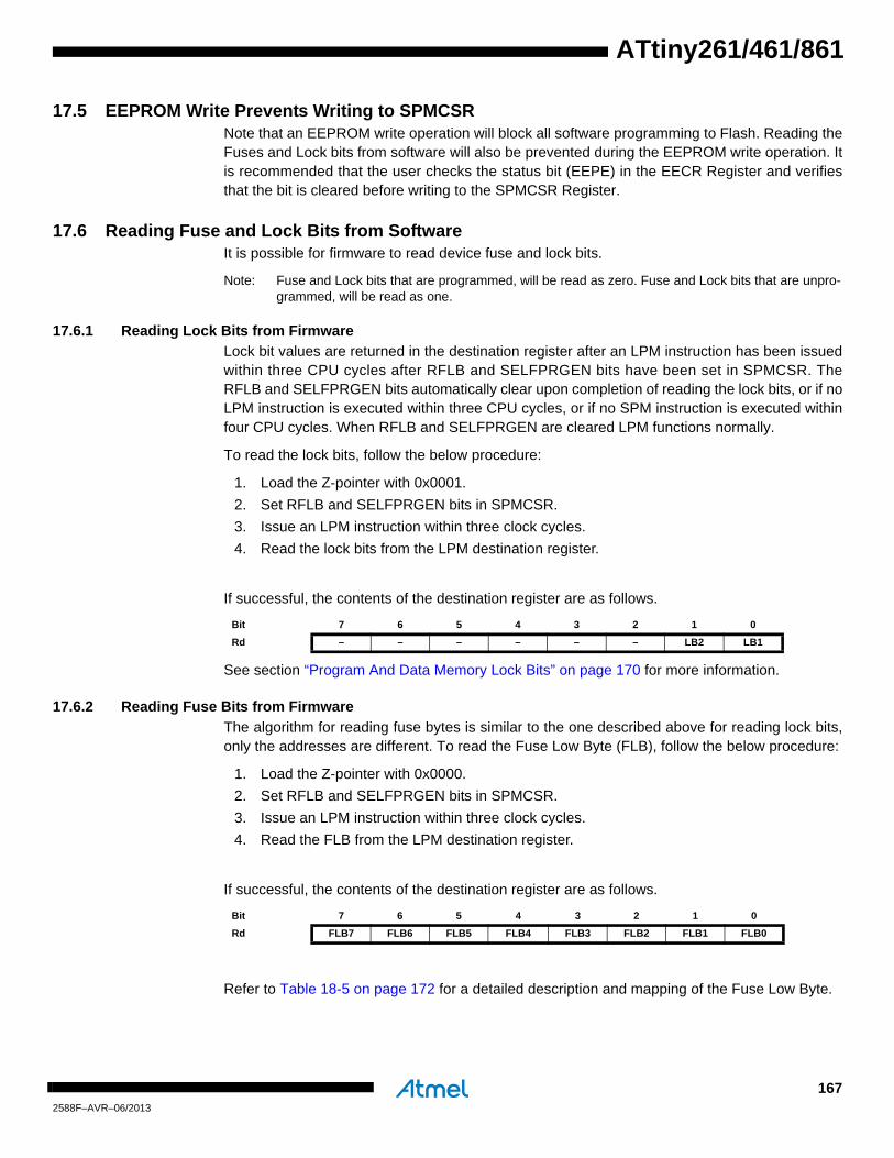
ATtiny261/461/861
17.5 EEPROM Write Prevents Writing to SPMCSRNote that an EEPROM write operation will block all software programming to Flash. Reading theFuses and Lock bits from software will also be prevented during the EEPROM write operation. Itis recommended that the user checks the status bit (EEPE) in the EECR Register and verifiesthat the bit is cleared before writing to the SPMCSR Register.
17.6 Reading Fuse and Lock Bits from SoftwareIt is possible for firmware to read device fuse and lock bits.
Note: Fuse and Lock bits that are programmed, will be read as zero. Fuse and Lock bits that are unpro-grammed, will be read as one.
17.6.1 Reading Lock Bits from Firmware
Lock bit values are returned in the destination register after an LPM instruction has been issuedwithin three CPU cycles after RFLB and SELFPRGEN bits have been set in SPMCSR. TheRFLB and SELFPRGEN bits automatically clear upon completion of reading the lock bits, or if noLPM instruction is executed within three CPU cycles, or if no SPM instruction is executed withinfour CPU cycles. When RFLB and SELFPRGEN are cleared LPM functions normally.
To read the lock bits, follow the below procedure:
1. Load the Z-pointer with 0x0001.
2. Set RFLB and SELFPRGEN bits in SPMCSR.
3. Issue an LPM instruction within three clock cycles.
4. Read the lock bits from the LPM destination register.
If successful, the contents of the destination register are as follows.
See section “Program And Data Memory Lock Bits” on page 170 for more information.
17.6.2 Reading Fuse Bits from Firmware
The algorithm for reading fuse bytes is similar to the one described above for reading lock bits,only the addresses are different. To read the Fuse Low Byte (FLB), follow the below procedure:
1. Load the Z-pointer with 0x0000.
2. Set RFLB and SELFPRGEN bits in SPMCSR.
3. Issue an LPM instruction within three clock cycles.
4. Read the FLB from the LPM destination register.
If successful, the contents of the destination register are as follows.
Refer to Table 18-5 on page 172 for a detailed description and mapping of the Fuse Low Byte.
Bit 7 6 5 4 3 2 1 0
Rd – – – – – – LB2 LB1
Bit 7 6 5 4 3 2 1 0
Rd FLB7 FLB6 FLB5 FLB4 FLB3 FLB2 FLB1 FLB0
1672588F–AVR–06/2013

To read the Fuse High Byte (FHB), simply replace the address in the Z-pointer with 0x0003 andrepeat the procedure above. If successful, the contents of the destination register are as follows.
Refer to Table 18-4 on page 171 for detailed description and mapping of the Fuse High Byte.
To read the Fuse Extended Byte (FEB), replace the address in the Z-pointer with 0x0002 andrepeat the previous procedure. If successful, the contents of the destination register are asfollows.
Refer to Table 18-3 on page 171 for detailed description and mapping of the Fuse ExtendedByte.
17.7 Preventing Flash CorruptionDuring periods of low VCC, the Flash program can be corrupted because the supply voltage istoo low for the CPU and the Flash to operate properly. These issues are the same as for boardlevel systems using the Flash, and the same design solutions should be applied.
A Flash program corruption can be caused by two situations when the voltage is too low. First, aregular write sequence to the Flash requires a minimum voltage to operate correctly. Secondly,the CPU itself can execute instructions incorrectly, if the supply voltage for executing instructionsis too low.
Flash corruption can easily be avoided by following these design recommendations (one issufficient):
1. Keep the AVR RESET active (low) during periods of insufficient power supply voltage. This can be done by enabling the internal Brown-out Detector (BOD) if the operating voltage matches the detection level. If not, an external low VCC reset protection circuit can be used. If a reset occurs while a write operation is in progress, the write operation will be completed provided that the power supply voltage is sufficient.
2. Keep the AVR core in Power-down sleep mode during periods of low VCC. This will pre-vent the CPU from attempting to decode and execute instructions, effectively protecting the SPMCSR Register and thus the Flash from unintentional writes.
17.8 Programming Time for Flash when Using SPMThe calibrated RC Oscillator is used to time Flash accesses. Table 17-1 shows the typical pro-gramming time for Flash accesses from the CPU.
Note: 1. Minimum and maximum programming time is per individual operation.
Bit 7 6 5 4 3 2 1 0
Rd FHB7 FHB6 FHB5 FHB4 FHB3 FHB2 FHB1 FHB0
Bit 7 6 5 4 3 2 1 0
Rd FEB7 FEB6 FEB5 FEB4 FEB3 FEB2 FEB1 FEB0
Table 17-1. SPM Programming Time(1)
Symbol Min Programming Time Max Programming Time
Flash write (Page Erase, Page Write, and write Lock bits by SPM)
3.7 ms 4.5 ms
1682588F–AVR–06/2013
ATtiny261/461/861

ATtiny261/461/861
17.9 Register Description
17.9.1 SPMCSR – Store Program Memory Control and Status Register
The Store Program Memory Control and Status Register contains the control bits needed to con-trol the Program memory operations.
• Bits 7:5 – Res: Reserved Bits
These bits are reserved and always read as zero.
• Bit 4 – CTPB: Clear Temporary Page Buffer
If the CTPB bit is written while filling the temporary page buffer, the temporary page buffer will becleared and the data will be lost.
• Bit 3 – RFLB: Read Fuse and Lock Bits
An LPM instruction within three cycles after RFLB and SPMEN are set in the SPMCSR Register,will read either the Lock bits or the Fuse bits (depending on Z0 in the Z-pointer) into the destina-tion register. See “EEPROM Write Prevents Writing to SPMCSR” on page 167 for details.
• Bit 2 – PGWRT: Page Write
If this bit is written to one at the same time as SPMEN, the next SPM instruction within four clockcycles executes Page Write, with the data stored in the temporary buffer. The page address istaken from the high part of the Z-pointer. The data in R1 and R0 are ignored. The PGWRT bitwill auto-clear upon completion of a Page Write, or if no SPM instruction is executed within fourclock cycles. The CPU is halted during the entire Page Write operation.
• Bit 1 – PGERS: Page Erase
If this bit is written to one at the same time as SPMEN, the next SPM instruction within four clockcycles executes Page Erase. The page address is taken from the high part of the Z-pointer. Thedata in R1 and R0 are ignored. The PGERS bit will auto-clear upon completion of a Page Erase,or if no SPM instruction is executed within four clock cycles. The CPU is halted during the entirePage Write operation.
• Bit 0 – SPMEN: Store Program Memory Enable
This bit enables the SPM instruction for the next four clock cycles. If written to one together witheither CTPB, RFLB, PGWRT, or PGERS, the following SPM instruction will have a specialmeaning, see description above. If only SPMEN is written, the following SPM instruction willstore the value in R1:R0 in the temporary page buffer addressed by the Z-pointer. The LSB ofthe Z-pointer is ignored. The SPMEN bit will auto-clear upon completion of an SPM instruction,or if no SPM instruction is executed within four clock cycles. During Page Erase and Page Write,the SPMEN bit remains high until the operation is completed.
Writing any other combination than “10001”, “01001”, “00101”, “00011” or “00001” in the lowerfive bits will have no effect.
Bit 7 6 5 4 3 2 1 0
0x37 (0x57) – – – CTPB RFLB PGWRT PGERS SPMEN SPMCSR
Read/Write R R R R/W R/W R/W R/W R/W
Initial Value 0 0 0 0 0 0 0 0
1692588F–AVR–06/2013

18. Memory ProgrammingThis section describes the different methods for programming ATtiny261/461/861 memories.
18.1 Program And Data Memory Lock BitsThe ATtiny261/461/861 provides two lock bits which can be left unprogrammed (“1”) or can beprogrammed (“0”) to obtain the additional security listed in Table 18-2. The lock bits can only beerased to “1” with the Chip Erase command.
The device has no separate boot loader section. The SPM instruction is enabled for the wholeFlash, if the SELFPROGEN fuse is programmed (“0”), otherwise it is disabled.
Program memory can be read out via the debugWIRE interface when the DWEN fuse is pro-grammed, even if lock bits are set. Thus, when lock bit security is required, debugWIRE shouldalways be disabled by clearing the DWEN fuse.
Note: “1” means unprogrammed, “0” means programmed.
Notes: 1. Program fuse bits before programming LB1 and LB2.
2. “1” means unprogrammed, “0” means programmed.
Lock bits can also be read by device firmware. See section “Reading Fuse and Lock Bits fromSoftware” on page 167.
Table 18-1. Lock Bit Byte
Lock Bit Byte Bit No Description Default Value
7 – 1 (unprogrammed)
6 – 1 (unprogrammed)
5 – 1 (unprogrammed)
4 – 1 (unprogrammed)
3 – 1 (unprogrammed)
2 – 1 (unprogrammed)
LB2 1 Lock bit 1 (unprogrammed)
LB1 0 Lock bit 1 (unprogrammed)
Table 18-2. Lock Bit Protection Modes.
Memory Lock Bits (1) (2) Protection Type
LB Mode LB2 LB1
1 1 1 No memory lock features enabled.
2 1 0Further programming of the Flash and EEPROM is disabled in High-voltage and Serial Programming mode. The Fuse bits are locked in both Serial and High-voltage Programming mode.(1)
3 0 0
Further programming and verification of the Flash and EEPROM is disabled in High-voltage and Serial Programming mode. The Fuse bits are locked in both Serial and High-voltage Programming mode.(1)
1702588F–AVR–06/2013
ATtiny261/461/861

ATtiny261/461/861
18.2 Fuse BytesThe ATtiny261/461/861 have three fuse bytes. Table 18-3, Table 18-4 and Table 18-5 describebriefly the functionality of all the fuses and how they are mapped into the fuse bytes. Note thatthe fuses are read as logical zero, “0”, if they are programmed.
Notes: 1. Enables SPM instruction. See “Self-Programming the Flash” on page 165.
Notes: 1. See “Alternate Functions of Port B” on page 66 for description of RSTDISBL and DWEN Fuses. After programming the RSTDISBL fuse, parallel programming must be used to change fuses and allow further programming.
2. DWEN must be unprogrammed when Lock Bit security is required. See “Program And Data Memory Lock Bits” on page 170.
3. The SPIEN Fuse is not accessible in SPI programming mode.
4. Programming this fues will disable the Watchdog Timer Interrupt. See “WDTCR – Watchdog Timer Control Register” on page 47 for details.
5. See Table 19-6 on page 191 for BODLEVEL Fuse decoding.
Table 18-3. Fuse Extended Byte
Fuse High Byte Bit No Description Default Value
7 - 1 (unprogrammed)
6 - 1 (unprogrammed)
5 - 1 (unprogrammed)
4 - 1 (unprogrammed)
3 - 1 (unprogrammed)
2 - 1 (unprogrammed)
1 - 1 (unprogrammed)
SELFPRGEN (1) 0 Self-Programming Enable 1 (unprogrammed)
Table 18-4. Fuse High Byte
Fuse High Byte Bit No Description Default Value
RSTDISBL (1) 7 External Reset disable 1 (unprogrammed)
DWEN (2) 6 DebugWIRE Enable 1 (unprogrammed)
SPIEN (3)) 6Enable Serial Program and Data Downloading
0 (programmed, SPI prog. enabled)
WDTON (4) 4 Watchdog Timer always on 1 (unprogrammed)
EESAVE 3EEPROM memory is preserved through the Chip Erase
1 (unprogrammed, EEPROM not preserved)
BODLEVEL2 (5) 2 Brown-out Detector trigger level 1 (unprogrammed)
BODLEVEL1 (5) 1 Brown-out Detector trigger level 1 (unprogrammed)
BODLEVEL0 (5) 0 Brown-out Detector trigger level 1 (unprogrammed)
1712588F–AVR–06/2013

Notes: 1. See “System Clock Prescaler” on page 31 for details.
2. Allows system clock to be output on pin. See “Clock Output Buffer” on page 32 for details.
3. The default value results in maximum start-up time for the default clock source. See Table 6-7 on page 28 for details.
4. The default setting results in internal RC Oscillator @ 8.0 MHz. See Table 6-6 on page 28 for details.
Note that fuse bits are locked if Lock Bit 1 (LB1) is programmed. Fuse bits should be pro-grammed before lock bits. The status of fuse bits is not affected by chip erase.
Fuse bits can also be read by device firmware. See section “Reading Fuse and Lock Bits fromSoftware” on page 167.
18.2.1 Latching of Fuses
Fuse values are latched when the device enters programming mode and changes to fuse valueshave no effect until the part leaves programming mode. This does not apply to the EESAVEFuse which will take effect once it is programmed. Fuses are also latched on power-up.
18.3 Signature BytesAll Atmel microcontrollers have a three-byte signature code which identifies the device. Thiscode can be read in both serial and High-voltage Programming mode, also when the device islocked. The three bytes reside in a separate address space. The ATtiny261/461/861signaturebytes are given in Table 18-6.
Table 18-5. Fuse Low Byte
Fuse Low Byte Bit No Description Default Value
CKDIV8 (1) 7 Divide clock by 8 0 (programmed)
CKOUT (2) 6 Clock Output Enable 1 (unprogrammed)
SUT1 5 Select start-up time 1 (unprogrammed) (3)
SUT0 4 Select start-up time 0 (programmed) (3)
CKSEL3 3 Select Clock source 0 (programmed) (4)
CKSEL2 2 Select Clock source 0 (programmed) (4)
CKSEL1 1 Select Clock source 1 (unprogrammed) (4)
CKSEL0 0 Select Clock source 0 (programmed) (4)
Table 18-6. Device ID
Parts
Signature Bytes Address
0x000 0x001 0x002
ATtiny261 0x1E 0x91 0x0C
ATtiny461 0x1E 0x92 0x08
ATtiny861 0x1E 0x93 0x0D
1722588F–AVR–06/2013
ATtiny261/461/861

ATtiny261/461/861
18.4 Calibration ByteSignature area of the ATtiny261/461/861 has one byte of calibration data for the internal RCOscillator. This byte resides in the high byte of address 0x000. During reset, this byte is auto-matically written into the OSCCAL Register to ensure correct frequency of the calibrated RCOscillator.
18.5 Page Size
18.6 Serial ProgrammingBoth the Flash and EEPROM memory arrays can be programmed using the serial SPI bus whileRESET is pulled to GND. The serial interface consists of pins SCK, MOSI (input) and MISO (out-put). See Figure 18-1.
Figure 18-1. Serial Programming and Verify
Note: If the device is clocked by the internal Oscillator, there is no need to connect a clock source to the CLKI pin.
Table 18-7. No. of Words in a Page and No. of Pages in the Flash
Device Flash Size Page Size PCWORD No. of Pages PCPAGE PCMSB
ATtiny261 1K words (2K bytes) 16 words PC[3:0] 64 PC[9:4] 9
ATtiny461 2K words (4K bytes) 32 words PC[4:0] 64 PC[10:5] 10
ATtiny861 4K words (8K bytes) 32 words PC[4:0] 128 PC[11:5] 11
Table 18-8. No. of Words in a Page and No. of Pages in the EEPROM
DeviceEEPROM
Size Page Size PCWORD No. of Pages PCPAGE EEAMSB
ATtiny261 128 bytes 4 bytes EEA[1:0] 32 EEA[6:2] 6
ATtiny461 256 bytes 4 bytes EEA[1:0] 64 EEA[7:2] 7
ATtiny861 512 bytes 4 bytes EEA[1:0] 128 EEA[8:2] 8
VCC
GND
SCK
MISO
MOSI
RESET
+1.8 - 5.5V
1732588F–AVR–06/2013

After RESET is set low, the Programming Enable instruction needs to be executed first beforeprogram/erase operations can be executed.
Note: In Table 18-9, above, the pin mapping for SPI programming is listed. Not all parts use the SPI pins dedicated for the internal SPI interface.
When programming the EEPROM, an auto-erase cycle is built into the self-timed programmingoperation (in the Serial mode ONLY) and there is no need to first execute the Chip Eraseinstruction. The Chip Erase operation turns the content of every memory location in both theProgram and EEPROM arrays into 0xFF.
Depending on CKSEL Fuses, a valid clock must be present. The minimum low and high periodsfor the serial clock (SCK) input are defined as follows:
• Low:> 2 CPU clock cycles for fck < 12 MHz, 3 CPU clock cycles for fck >= 12 MHz
• High:> 2 CPU clock cycles for fck < 12 MHz, 3 CPU clock cycles for fck >= 12 MHz
18.6.1 Serial Programming Algorithm
When writing serial data to the ATtiny261/461/861, data is clocked on the rising edge of SCK.When reading, data is clocked on the falling edge of SCK. See Figure 19-4 and Figure 19-5 fortiming details.
To program and verify the ATtiny261/461/861 in the Serial Programming mode, the followingsequence is recommended (see four byte instruction formats in Table 18-11):
1. Power-up sequence:Apply power between VCC and GND while RESET and SCK are set to “0”. In some sys-tems, the programmer can not guarantee that SCK is held low during power-up. In this case, RESET must be given a positive pulse after SCK has been set to '0'. The duration of the pulse must be at least tRST (the minimum pulse width on RESET pin, see Table 19-4 on page 190) plus two CPU clock cycles.
2. Wait for at least 20 ms and enable serial programming by sending the Programming Enable serial instruction to pin MOSI.
3. The serial programming instructions will not work if the communication is out of syn-chronization. When in sync. the second byte (0x53), will echo back when issuing the third byte of the Programming Enable instruction. Whether the echo is correct or not, all four bytes of the instruction must be transmitted. If the 0x53 did not echo back, give RESET a positive pulse and issue a new Programming Enable command.
4. The Flash is programmed one page at a time. The memory page is loaded one byte at a time by supplying the 5 LSB of the address and data together with the Load Program memory Page instruction. To ensure correct loading of the page, the data low byte must be loaded before data high byte is applied for a given address. The Program memory Page is stored by loading the Write Program memory Page instruction with the 6 MSB of the address. If polling (RDY/BSY) is not used, the user must wait at least tWD_FLASH before issuing the next page. (See Table 18-10.) Accessing the serial programming
Table 18-9. Pin Mapping Serial Programming
Symbol Pins I/O Description
MOSI PB0 I Serial Data in
MISO PB1 O Serial Data out
SCK PB2 I Serial Clock
1742588F–AVR–06/2013
ATtiny261/461/861

ATtiny261/461/861
interface before the Flash write operation completes can result in incorrect programming.
5. A: The EEPROM array is programmed one byte at a time by supplying the address and data together with the appropriate Write instruction. An EEPROM memory location is first automatically erased before new data is written. If polling (RDY/BSY) is not used, the user must wait at least tWD_EEPROM before issuing the next byte. (See Table 18-10.) In a chip erased device, no 0xFFs in the data file(s) need to be programmed.B: The EEPROM array is programmed one page at a time. The Memory page is loaded one byte at a time by supplying the 2 LSB of the address and data together with the Load EEPROM Memory Page instruction. The EEPROM Memory Page is stored by loading the Write EEPROM Memory Page Instruction with the 6 MSB of the address. When using EEPROM page access only byte locations loaded with the Load EEPROM Memory Page instruction is altered. The remaining locations remain unchanged. If poll-ing (RDY/BSY) is not used, the used must wait at least tWD_EEPROM before issuing the next page (See Table 18-8). In a chip erased device, no 0xFF in the data file(s) need to be programmed.
6. Any memory location can be verified by using the Read instruction which returns the content at the selected address at serial output MISO.
7. At the end of the programming session, RESET can be set high to commence normal operation.
8. Power-off sequence (if needed):Set RESET to “1”.Turn VCC power off.
18.6.2 Serial Programming Instruction set
The instruction set is described in Table 18-11 on page 176 and Figure 18-2 on page 177.
Table 18-10. Minimum Wait Delay Before Writing the Next Flash or EEPROM Location
Symbol Minimum Wait Delay
tWD_FLASH 4.5 ms
tWD_EEPROM 4.0 ms
tWD_ERASE 9.0 ms
tWD_FUSE 4.5 ms
1752588F–AVR–06/2013

Notes: 1. Not all instructions are applicable for all parts.
2. a = address
3. Bits are programmed ‘0’, unprogrammed ‘1’.
4. To ensure future compatibility, unused Fuses and Lock bits should be unprogrammed (‘1’) .
5. Refer to the correspondig section for Fuse and Lock bits, Calibration and Signature bytes and Page size.
6. Instructions accessing program memory use a word address. This address may be random within the page range.
7. See http://www.atmel.com/avr for Application Notes regarding programming and programmers.
Table 18-11. Serial Programming Instruction Set
Instruction/Operation
Instruction Format
Byte 1 Byte 2 Byte 3 Byte4
Programming Enable $AC $53 $00 $00
Chip Erase (Program Memory/EEPROM) $AC $80 $00 $00
Poll RDY/BSY $F0 $00 $00 data byte out
Load Instructions
Load Extended Address byte(1) $4D $00 Extended adr $00
Load Program Memory Page, High byte $48 adr MSB adr LSB high data byte in
Load Program Memory Page, Low byte $40 adr MSB adr LSB low data byte in
Load EEPROM Memory Page (page access) $C1 $00 0000 000aa data byte in
Read Instructions
Read Program Memory, High byte $28 adr MSB adr LSB high data byte out
Read Program Memory, Low byte $20 adr MSB adr LSB low data byte out
Read EEPROM Memory $A0 $00 00aa aaaa data byte out
Read Lock bits $58 $00 $00 data byte out
Read Signature Byte $30 $00 0000 000aa data byte out
Read Fuse bits $50 $00 $00 data byte out
Read Fuse High bits $58 $08 $00 data byte out
Read Extended Fuse Bits $50 $08 $00 data byte out
Read Calibration Byte $38 $00 $00 data byte out
Write Instructions(6)
Write Program Memory Page $4C adr MSB adr LSB $00
Write EEPROM Memory $C0 $00 00aa aaaa data byte in
Write EEPROM Memory Page (page access) $C2 $00 00aa aa00 $00
Write Lock bits $AC $E0 $00 data byte in
Write Fuse bits $AC $A0 $00 data byte in
Write Fuse High bits $AC $A8 $00 data byte in
Write Extended Fuse Bits $AC $A4 $00 data byte in
1762588F–AVR–06/2013
ATtiny261/461/861

ATtiny261/461/861
Figure 18-2. Serial Programming Instruction example
If the LSB in RDY/BSY data byte out is ‘1’, a programming operation is still pending. Wait untilthis bit returns ‘0’ before the next instruction is carried out.
Within the same page, the low data byte must be loaded prior to the high data byte.
After data is loaded to the page buffer, program the EEPROM page, see Figure 18-2 on page177.
18.7 Parallel Programming
This section describes how to parallel program and verify Flash Program memory, EEPROMData memory, Memory Lock bits, and Fuse bits. Pulses are assumed to be at least 250 ns inlength, unless otherwise noted.
18.7.1 Signal Names
In this section, some pins are referenced by signal names describing their functionality duringparallel programming, see Figure 18-3 and Table 18-12. Pins not described in the following tableare referenced by pin names.
Byte 1 Byte 2 Byte 3 Byte 4
Adr MSB Adr LSB
Bit 15 B 0
Serial Programming Instruction
Program Memory/EEPROM Memory
Page 0
Page 1
Page 2
Page N-1
Page Buffer
Write Program Memory Page/Write EEPROM Memory Page
Load Program Memory Page (High/Low Byte)/Load EEPROM Memory Page (page access)
Byte 1 Byte 2 Byte 3 Byte 4
Bit 15 B 0
Adr MSB Adr LSB
Page Offset
Page Number
Adrdr Mr MSSBA AAdrdr LS LSBSB
1772588F–AVR–06/2013

Figure 18-3. Parallel Programming.
Table 18-12. Pin Name Mapping
Signal Name in Programming Mode
Pin Name I/O Function
WR PB0 I Write Pulse (Active low).
XA0 PB1 I XTAL Action Bit 0
XA1/BS2 PB2 IXTAL Action Bit 1. Byte Select 2 (“0” selects low byte, “1” selects 2’nd high byte).
PAGEL/BS1 PB3 IByte Select 1 (“0” selects low byte, “1” selects high byte). Program Memory and EEPROM Data Page Load.
OE PB5 I Output Enable (Active low).
RDY/BSY PB6 O0: Device is busy programming, 1: Device is ready for new command.
DATA I/O PA7-PA0 I/O Bi-directional Data bus (Output when OE is low).
VCC
+5V
GND
XTAL1/PB4
PB6
PB5
PB0
PB3
PB1
PB2
PA7 - PA0 DATA
RESET +12 V
PAGEL/BS1
XA0
XA1/BS2
OE
RDY/BSY
WR
AVCC
+5V
1782588F–AVR–06/2013
ATtiny261/461/861

ATtiny261/461/861
The XA1/XA0 pins determine the action executed when the XTAL1 pin is given a positive pulse.The bit coding is shown in Table 18-14.
When pulsing WR or OE, the command loaded determines the action executed. The differentCommands are shown in Table 18-15.
18.7.2 Entering Programming Mode
The following algorithm puts the device in parallel programming mode:
1. Apply 4.5 - 5.5V between VCC and GND.
2. Set RESET to “0” and toggle XTAL1 at least six times.
3. Set Prog_enable pins listed in Table 18-13 on page 179 to “0000” and wait at least 100 ns.
4. Apply 11.5 - 12.5V to RESET. Any activity on Prog_enable pins within 100 ns after +12V has been applied to RESET, will cause the device to fail entering programming mode.
5. Wait at least 50 µs before sending a new command.
Table 18-13. Pin Values Used to Enter Programming Mode
Pin Symbol Value
PAGEL/BS1 Prog_enable[3] 0
XA1/BS2 Prog_enable[2] 0
XA0 Prog_enable[1] 0
WR Prog_enable[0] 0
Table 18-14. XA1 and XA0 Coding
XA1 XA0 Action when XTAL1 is Pulsed
0 0 Load Flash or EEPROM Address (High or low address byte determined by BS1).
0 1 Load Data (High or Low data byte for Flash determined by BS1).
1 0 Load Command
1 1 No Action, Idle
Table 18-15. Command Byte Bit Coding
Command Byte Command Executed
1000 0000 Chip Erase
0100 0000 Write Fuse bits
0010 0000 Write Lock bits
0001 0000 Write Flash
0001 0001 Write EEPROM
0000 1000 Read Signature Bytes and Calibration byte
0000 0100 Read Fuse and Lock bits
0000 0010 Read Flash
0000 0011 Read EEPROM
1792588F–AVR–06/2013
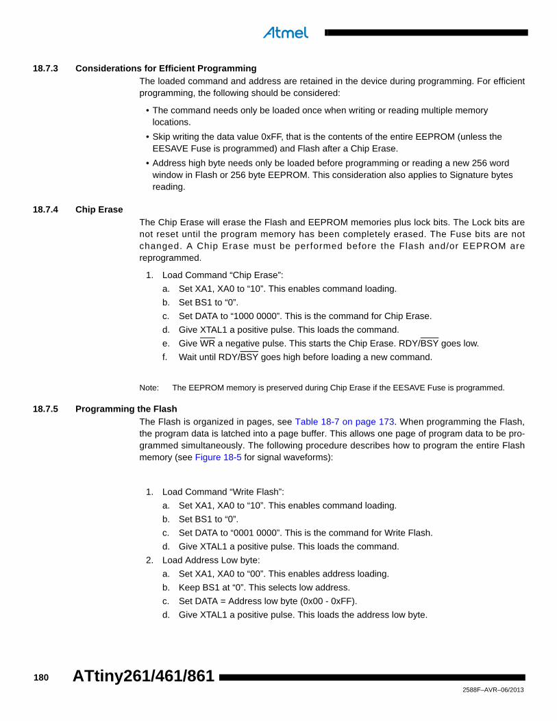
18.7.3 Considerations for Efficient Programming
The loaded command and address are retained in the device during programming. For efficientprogramming, the following should be considered:
• The command needs only be loaded once when writing or reading multiple memory locations.
• Skip writing the data value 0xFF, that is the contents of the entire EEPROM (unless the EESAVE Fuse is programmed) and Flash after a Chip Erase.
• Address high byte needs only be loaded before programming or reading a new 256 word window in Flash or 256 byte EEPROM. This consideration also applies to Signature bytes reading.
18.7.4 Chip Erase
The Chip Erase will erase the Flash and EEPROM memories plus lock bits. The Lock bits arenot reset until the program memory has been completely erased. The Fuse bits are notchanged. A Chip Erase must be performed before the Flash and/or EEPROM arereprogrammed.
1. Load Command “Chip Erase”:
a. Set XA1, XA0 to “10”. This enables command loading.
b. Set BS1 to “0”.
c. Set DATA to “1000 0000”. This is the command for Chip Erase.
d. Give XTAL1 a positive pulse. This loads the command.
e. Give WR a negative pulse. This starts the Chip Erase. RDY/BSY goes low.
f. Wait until RDY/BSY goes high before loading a new command.
Note: The EEPROM memory is preserved during Chip Erase if the EESAVE Fuse is programmed.
18.7.5 Programming the Flash
The Flash is organized in pages, see Table 18-7 on page 173. When programming the Flash,the program data is latched into a page buffer. This allows one page of program data to be pro-grammed simultaneously. The following procedure describes how to program the entire Flashmemory (see Figure 18-5 for signal waveforms):
1. Load Command “Write Flash”:
a. Set XA1, XA0 to “10”. This enables command loading.
b. Set BS1 to “0”.
c. Set DATA to “0001 0000”. This is the command for Write Flash.
d. Give XTAL1 a positive pulse. This loads the command.
2. Load Address Low byte:
a. Set XA1, XA0 to “00”. This enables address loading.
b. Keep BS1 at “0”. This selects low address.
c. Set DATA = Address low byte (0x00 - 0xFF).
d. Give XTAL1 a positive pulse. This loads the address low byte.
1802588F–AVR–06/2013
ATtiny261/461/861

ATtiny261/461/861
3. Load Data Low Byte:
a. Set XA1, XA0 to “01”. This enables data loading.
b. Set DATA = Data low byte (0x00 - 0xFF).
c. Give XTAL1 a positive pulse. This loads the data byte.
4. Load Data High Byte:
a. Set BS1 to “1”. This selects high data byte.
b. Keep XA1, XA0 at “01”. This enables data loading.
c. Set DATA = Data high byte (0x00 - 0xFF).
d. Give XTAL1 a positive pulse. This loads the data byte.
5. Repeat steps 2 to 4 until the entire buffer is filled or until all data within the page is loaded.
6. Load Address High byte:
a. Set XA1, XA0 to “00”. This enables address loading.
b. Set BS1 to “1”. This selects high address.
c. Set DATA = Address high byte (0x00 - 0xFF).
d. Give XTAL1 a positive pulse. This loads the address high byte.
7. Program Page:
a. Give WR a negative pulse. This starts programming of the entire page of data. RDY/BSY goes low.
b. Wait until RDY/BSY goes high.
8. Repeat steps 2 to 7 until the entire Flash is programmed or until all data has been programmed.
9. End Page Programming:
a. Set XA1, XA0 to “10”. This enables command loading.
b. Set DATA to “0000 0000”. This is the command for No Operation.
c. Give XTAL1 a positive pulse. This loads the command, and the internal write sig-nals are reset.
While the lower bits in the address are mapped to words within the page, the higher bits addressthe pages within the FLASH. This is illustrated in Figure 18-4. Note that if less than eight bits arerequired to address words in the page (pagesize < 256), the most significant bit(s) in the addresslow byte are used to address the page when performing a Page Write.
1812588F–AVR–06/2013

Figure 18-4. Addressing the Flash Which is Organized in Pages
Note: PCPAGE and PCWORD are listed in Table 18-7 on page 173.
In the figure below, “XX” means don’t care. The numbers in the figure refer to the programmingdescription above.
WR
Figure 18-5. Flash Programming Waveforms
18.7.6 Programming the EEPROM
The EEPROM is organized in pages, see Table 18-8 on page 173. When programming theEEPROM, the program data is latched into a page buffer. This allows one page of data to be
PROGRAM MEMORY
WORD ADDRESSWITHIN A PAGE
PAGE ADDRESSWITHIN THE FLASH
INSTRUCTION WORD
PAGE PCWORD[PAGEMSB:0]:
00
01
02
PAGEEND
PAGE
PCWORDPCPAGE
PCMSB PAGEMSBPROGRAMCOUNTER
0x10 ADDR. LOW DATA LOW ADDR. HIGHDATA HIGHDATA LOWADDR. LOWDATA HIGHDATA
XA1 / BS2
XA0
PAGEL / BS1
XTAL1
WR
RDY / BSY
RESET +12V
OE
XXX
1
STEP
7
5
6432432
8
0x00
9
1822588F–AVR–06/2013
ATtiny261/461/861

ATtiny261/461/861
programmed simultaneously. The programming algorithm for the EEPROM data memory is asfollows (refer to “Programming the Flash” on page 180 for details on Command, Address andData loading):
1. A: Load Command “0001 0001”.
2. G: Load Address High Byte (0x00 - 0xFF).
3. B: Load Address Low Byte (0x00 - 0xFF).
4. C: Load Data (0x00 - 0xFF).
5. E: Latch data (give PAGEL a positive pulse).
6. K: Repeat 3 through 5 until the entire buffer is filled.
7. L: Program EEPROM page
a. Set BS to “0”.
b. Give WR a negative pulse. This starts programming of the EEPROM page. RDY/BSY goes low.
c. Wait until to RDY/BSY goes high before programming the next page (See Figure 18-6 for signal waveforms).
Figure 18-6. Programming the EEPROM Waveforms
18.7.7 Reading the Flash
The algorithm for reading the Flash memory is as follows (refer to “Programming the Flash” onpage 180 for details on Command and Address loading):
1. A: Load Command “0000 0010”.
2. G: Load Address High Byte (0x00 - 0xFF).
3. B: Load Address Low Byte (0x00 - 0xFF).
4. Set OE to “0”, and BS1 to “0”. The Flash word low byte can now be read at DATA.
5. Set BS to “1”. The Flash word high byte can now be read at DATA.
6. Set OE to “1”.
RDY/BSY
WR
OE
RESET +12V
0x11 ADDR. HIGHDATA
ADDR. LOW DATA ADDR. LOW DATA XX
XA1/BS2
XA0
PAGEL/BS1
XTAL1
XX
A G B C E B C E L
K
1832588F–AVR–06/2013

18.7.8 Reading the EEPROM
The algorithm for reading the EEPROM memory is as follows (refer to “Programming the Flash”on page 180 for details on Command and Address loading):
1. A: Load Command “0000 0011”.
2. G: Load Address High Byte (0x00 - 0xFF).
3. B: Load Address Low Byte (0x00 - 0xFF).
4. Set OE to “0”, and BS1 to “0”. The EEPROM Data byte can now be read at DATA.
5. Set OE to “1”.
18.7.9 Programming the Fuse Low Bits
The algorithm for programming the Fuse Low bits is as follows (refer to “Programming the Flash”on page 180 for details on Command and Data loading):
1. A: Load Command “0100 0000”.
2. C: Load Data Low Byte. Bit n = “0” programs and bit n = “1” erases the Fuse bit.
3. Give WR a negative pulse and wait for RDY/BSY to go high.
18.7.10 Programming the Fuse High Bits
The algorithm for programming the Fuse High bits is as follows (refer to “Programming theFlash” on page 180 for details on Command and Data loading):
1. A: Load Command “0100 0000”.
2. C: Load Data Low Byte. Bit n = “0” programs and bit n = “1” erases the Fuse bit.
3. Set BS1 to “1” and BS2 to “0”. This selects high data byte.
4. Give WR a negative pulse and wait for RDY/BSY to go high.
5. Set BS1 to “0”. This selects low data byte.
18.7.11 Programming the Extended Fuse Bits
The algorithm for programming the Extended Fuse bits is as follows (refer to “Programming theFlash” on page 180 for details on Command and Data loading):
1. 1. A: Load Command “0100 0000”.
2. 2. C: Load Data Low Byte. Bit n = “0” programs and bit n = “1” erases the Fuse bit.
3. 3. Set BS1 to “0” and BS2 to “1”. This selects extended data byte.
4. 4. Give WR a negative pulse and wait for RDY/BSY to go high.
5. 5. Set BS2 to “0”. This selects low data byte.
1842588F–AVR–06/2013
ATtiny261/461/861

ATtiny261/461/861
Figure 18-7. Programming the FUSES Waveforms
18.7.12 Programming the Lock Bits
The algorithm for programming the Lock bits is as follows (refer to “Programming the Flash” onpage 180 for details on Command and Data loading):
1. A: Load Command “0010 0000”.
2. C: Load Data Low Byte. Bit n = “0” programs the Lock bit. If LB mode 3 is programmed (LB1 and LB2 is programmed), it is not possible to program the Boot Lock bits by any External Programming mode.
3. Give WR a negative pulse and wait for RDY/BSY to go high.
The Lock bits can only be cleared by executing Chip Erase.
18.7.13 Reading the Fuse and Lock Bits
The algorithm for reading the Fuse and Lock bits is as follows (refer to “Programming the Flash”on page 180 for details on Command loading):
1. A: Load Command “0000 0100”.
2. Set OE to “0”, BS2 to “0” and BS1 to “0”. The status of the Fuse Low bits can now be read at DATA (“0” means programmed).
3. Set OE to “0”, BS2 to “1” and BS1 to “1”. The status of the Fuse High bits can now be read at DATA (“0” means programmed).
4. Set OE to “0”, BS2 to “1”, and BS1 to “0”. The status of the Extended Fuse bits can now be read at DATA (“0” means programmed).
5. Set OE to “0”, BS2 to “0” and BS1 to “1”. The status of the Lock bits can now be read at DATA (“0” means programmed).
6. Set OE to “1”.
RDY/BSY
WR
OE
RESET +12V
0x40DATA
DATA XX
XA1/BS2
XA0
PAGEL/BS1
XTAL1
A C
0x40 DATA XX
A C
Write Fuse Low byte Write Fuse high byte
0x40 DATA XX
A C
Write Extended Fuse byte
1852588F–AVR–06/2013

Figure 18-8. Mapping Between BS1, BS2 and the Fuse and Lock Bits During Read
18.7.14 Reading the Signature Bytes
The algorithm for reading the Signature bytes is as follows (refer to “Programming the Flash” onpage 180 for details on Command and Address loading):
1. A: Load Command “0000 1000”.
2. B: Load Address Low Byte (0x00 - 0x02).
3. Set OE to “0”, and BS to “0”. The selected Signature byte can now be read at DATA.
4. Set OE to “1”.
18.7.15 Reading the Calibration Byte
The algorithm for reading the Calibration byte is as follows (refer to “Programming the Flash” onpage 180 for details on Command and Address loading):
1. A: Load Command “0000 1000”.
2. B: Load Address Low Byte, 0x00.
3. Set OE to “0”, and BS1 to “1”. The Calibration byte can now be read at DATA.
4. Set OE to “1”.
Lock Bits 0
1
BS2
Fuse High Byte
0
1
BS1
DATA
Fuse Low Byte 0
1
BS2
Extended Fuse Byte
1862588F–AVR–06/2013
ATtiny261/461/861
ATtiny261/461/861
19. Electrical Characteristics
19.1 Absolute Maximum Ratings*
19.2 DC Characteristics
Operating Temperature.................................. -55C to +125C *NOTICE: Stresses beyond those listed under “Absolute Maximum Ratings” may cause permanent dam-age to the device. This is a stress rating only and functional operation of the device at these or other conditions beyond those indicated in the operational sections of this specification is not implied. Exposure to absolute maximum rating conditions for extended periods may affect device reliability.
Storage Temperature ..................................... -65°C to +150°C
Voltage on any Pin except RESETwith respect to Ground ................................-0.5V to VCC+0.5V
Voltage on RESET with respect to Ground......-0.5V to +13.0V
Maximum Operating Voltage ............................................ 6.0V
DC Current per I/O Pin ............................................... 40.0 mA
DC Current VCC and GND Pins ................................ 200.0 mA
Table 19-1. DC Characteristics. TA = -40C to +85C, VCC = 1.8V to 5.5V (unless otherwise noted).
Symbol Parameter Condition Min Typ (1) Max Units
VIL Input Low-voltage
Except XTAL1 andRESET pins
-0.5 0.2VCC(3) V
XTAL1 pin,External Clock Selected
-0.5 0.1VCC(3) V
RESET pin -0.5 0.2VCC(3) V
RESET pin as I/O -0.5 0.2VCC(3) V
VIH Input High-voltage
Except XTAL1 andRESET pins
0.7VCC(2) VCC +0.5 V
XTAL1 pin,External Clock Selected
0.8VCC(2) VCC +0.5 V
RESET pin 0.9VCC(2) VCC +0.5 V
RESET pin as I/O 0.7VCC(2) VCC +0.5 V
VOLOutput Low Voltage (4)
(Except Reset pin) (6)IOL = 10 mA, VCC = 5VIOL = 5 mA, VCC = 3V
0.60.5
VV
VOHOutput High-voltage (5)
(Except Reset pin) (6)IOH = -10 mA, VCC = 5VIOH = -5 mA, VCC = 3V
4.32.5
VV
IILInput LeakageCurrent I/O Pin
Vcc = 5.5V, pin low(absolute value)
< 0.05 1 µA
IIHInput LeakageCurrent I/O Pin
Vcc = 5.5V, pin high(absolute value)
< 0.05 1 µA
RRST Reset Pull-up Resistor 30 60 k
RPU I/O Pin Pull-up Resistor 20 50 k
1872588F–AVR–06/2013

Notes: 1. Typical values at +25C.
2. “Min” means the lowest value where the pin is guaranteed to be read as high.
3. “Max” means the highest value where the pin is guaranteed to be read as low.
4. Although each I/O port can sink more than the test conditions (10 mA at VCC = 5V, 5 mA at VCC = 3V) under steady state conditions (non-transient), the sum of all IOL (for all ports) should not exceed 60 mA. If IOL exceeds the test conditions, VOL may exceed the related specification. Pins are not guaranteed to sink current greater than the listed test condition.
5. Although each I/O port can source more than the test conditions (10 mA at VCC = 5V, 5 mA at VCC = 3V) under steady state conditions (non-transient), the sum of all IOH (for all ports) should not exceed 60 mA. If IOH exceeds the test condition, VOH may exceed the related specification. Pins are not guaranteed to source current greater than the listed test condition.
6. The RESET pin must tolerate high voltages when entering and operating in programming modes and, as a consequence, has a weak drive strength as compared to regular I/O pins. See Figure 20-23, Figure 20-24, Figure 20-25, and Figure 20-26 (starting on page 209).
7. Values are with external clock using methods described in “Minimizing Power Consumption” on page 37. Power Reduction is enabled (PRR = 0xFF) and there is no I/O drive.
8. BOD Disabled.
19.3 SpeedThe maximum operating frequency of the device depends on VCC. As shown in Figure 19-1 andFigure 19-2, the maximum frequency vs. VCC relationship is linear between 1.8V < VCC < 2.7Vand between 2.7V < VCC < 4.5V.
Figure 19-1. Maximum Frequency vs. VCC (ATtiny261V/461V/861V)
ICC
Power Supply Current (7)
Active 1MHz, VCC = 2V 0.4 0.6 mA
Active 4MHz, VCC = 3V 2 3 mA
Active 8MHz, VCC = 5V 6 9 mA
Idle 1MHz, VCC = 2V 0.1 0.3 mA
Idle 4MHz, VCC = 3V 0.4 1 mA
Idle 8MHz, VCC = 5V 1.5 3 mA
Power-down mode (8)WDT enabled, VCC = 3V 4 10 µA
WDT disabled, VCC = 3V 0.15 2 µA
Table 19-1. DC Characteristics. TA = -40C to +85C, VCC = 1.8V to 5.5V (unless otherwise noted).
Symbol Parameter Condition Min Typ (1) Max Units
10 MHz
4 MHz
1.8V 2.7V 5.5V
Safe Operating Area
1882588F–AVR–06/2013
ATtiny261/461/861

ATtiny261/461/861
Figure 19-2. Maximum Frequency vs. VCC (ATtiny261/461/861)
19.4 Clock CharacteristicsIt is possible to manually calibrate the internal oscillator to be more accurate than default factorycalibration. Note that the oscillator frequency depends on temperature and voltage. Voltage andtemperature characteristics can be found in Figure 20-38 on page 217 and Figure 20-39 onpage 217.
Notes: 1. Accuracy of oscillator frequency at calibration point (fixed temperature and fixed voltage).
2. Voltage range for ATtiny261V/461V/861V.
3. Voltage range for ATtiny261/461/861.
Figure 19-3. External Clock Drive Waveforms
20 MHz
10 MHz
2.7V 4.5V 5.5V
Safe Operating Area
Table 19-2. Calibration Accuracy of Internal RC Oscillator
CalibrationMethod Target Frequency VCC Temperature
Accuracy at givenvoltage & temperature (1)
FactoryCalibration
8.0 MHz 3V 25C ±10%
UserCalibration
Fixed frequency within:
7.3 - 8.1 MHz
Fixed voltage within:1.8 - 5.5V(2)
2.7 - 5.5V(3)
Fixed temperature within:
-40C to +85C±1%
VIL1
VIH1
1892588F–AVR–06/2013

19.5 System and Reset Characteristics
Note: 1. Values are guidelines, only.
19.5.1 Power-On Reset
Notes: 1. Values are guidelines, only.
2. Threshold where device is released from reset when voltage is rising
3. The power-on reset will not work unless the supply voltage has been below VPOA
Table 19-3. External Clock Drive Characteristics
Symbol Parameter
VCC = 1.8 - 5.5V VCC = 2.7 - 5.5V VCC = 4.5 - 5.5V
UnitsMin. Max. Min. Max. Min. Max.
1/tCLCL Clock Frequency 0 4 0 10 0 20 MHz
tCLCL Clock Period 250 100 50 ns
tCHCX High Time 100 40 20 ns
tCLCX Low Time 100 40 20 ns
tCLCH Rise Time 2.0 1.6 0.5 s
tCHCL Fall Time 2.0 1.6 0.5 s
tCLCL Change in period from one clock cycle to the next 2 2 2 %
Table 19-4. Reset, Brown-out, and Internal Voltage Characteristics
Symbol Parameter Condition Min Typ Max Units
VRST RESET Pin Threshold Voltage (1) 0.2 VCC 0.9 VCC V
tRSTMinimum pulse width onRESET Pin (1) VCC = 3V 2.5 µs
VHYST Brown-out Detector Hysteresis (1) 50 mV
tBODMin Pulse Width onBrown-out Reset (1) 2 µs
VBGInternal bandgap referencevoltage
VCC = 2.7VTA = 25°C
1.0 1.1 1.2 V
tBGInternal bandgap referencestart-up time (1)
VCC = 5VTA = 25°C
40 70 µs
IBGInternal bandgap referencecurrent consumption (1)
VCC = 5VTA = 25°C
15 µA
Table 19-5. Characteristics of Power-On Reset. TA = -40 to +85C
Symbol Parameter Min(1) Typ(1) Max(1) Units
VPOR Release threshold of power-on reset (2) 0.7 1.0 1.4 V
VPOA Activation threshold of power-on reset (3) 0.05 0.9 1.3 V
SRON Power-on slope rate 0.01 4.5 V/ms
1902588F–AVR–06/2013
ATtiny261/461/861

ATtiny261/461/861
19.5.2 Brown-Out Detection
Note: 1. VBOT may be below nominal minimum operating voltage for some devices. For devices where this is the case, the device is tested down to VCC = VBOT during the production test. This guar-antees that a Brown-out Reset will occur before VCC drops to a voltage where correct operation of the microcontroller is no longer guaranteed.
Table 19-6. BODLEVEL Fuse Coding(1)
BODLEVEL[2:0] Fuses Min VBOT Typ VBOT Max VBOT Units
111 BOD Disabled
110 1.7 1.8 2.0
V101 2.5 2.7 2.9
100 4.1 4.3 4.5
0XX Reserved
1912588F–AVR–06/2013

19.6 ADC Characteristics
Note: 1. Values are guidelines, only.
2. VDIFF must be below VREF.
Table 19-7. ADC Characteristics, Single Ended Channels. T = -40C to +85C
Symbol Parameter Condition Min(1) Typ(1) Max(1) Units
Resolution 10 Bits
Absolute accuracy(Including INL, DNL, and Quantization, Gain and Offset Errors)
VREF = 4V, VCC = 4V,ADC clock = 200 kHz
2 LSB
VREF = 4V, VCC = 4V,ADC clock = 1 MHz
3 LSB
VREF = 4V, VCC = 4V,ADC clock = 200 kHz
Noise Reduction Mode1.5 LSB
VREF = 4V, VCC = 4V,ADC clock = 1 MHzNoise Reduction Mode
2.5 LSB
Integral Non-Linearity (INL)(Accuracy after Offset and Gain Calibration)
VREF = 4V, VCC = 4V,ADC clock = 200 kHz
1 LSB
Differential Non-linearity (DNL)VREF = 4V, VCC = 4V,ADC clock = 200 kHz
0.5 LSB
Gain ErrorVREF = 4V, VCC = 4V,ADC clock = 200 kHz
2.5 LSB
Offset ErrorVREF = 4V, VCC = 4V,ADC clock = 200 kHz
1.5 LSB
Conversion Time Free Running Conversion 13 260 µs
Clock Frequency 50 1000 kHz
AVCC Analog Supply Voltage VCC - 0.3 VCC + 0.3 V
AREF External Voltage Reference Single Ended Conversions 2.0 AVCC V
Differential Conversions 2.0 AVCC - 1.0 V
VIN Input VoltageSingle Ended Conversions GND VREF
Differential Conversions 0 AVCC (2) V
Input BandwidthSingle Ended Conversions 38.5
kHzDifferential Conversions 4
VINT
Internal 1.1V Reference 1.0 1.1 1.2 V
Internal 2.56V Reference (2) 2.3 2.56 2.8 V
RREF Reference Input Resistance 35 k
RAIN Analog Input Resistance 100 M
ADC Conversion Output 0 1023 LSB
1922588F–AVR–06/2013
ATtiny261/461/861
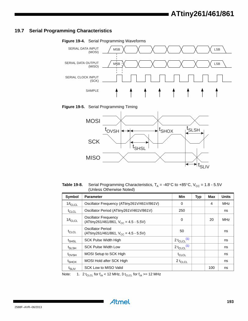
ATtiny261/461/861
19.7 Serial Programming Characteristics
Figure 19-4. Serial Programming Waveforms
Figure 19-5. Serial Programming Timing
Note: 1. 2 tCLCL for fck < 12 MHz, 3 tCLCL for fck >= 12 MHz
Table 19-8. Serial Programming Characteristics, TA = -40C to +85C, VCC = 1.8 - 5.5V (Unless Otherwise Noted)
Symbol Parameter Min Typ Max Units
1/tCLCL Oscillator Frequency (ATtiny261V/461V/861V) 0 4 MHz
tCLCL Oscillator Period (ATtiny261V/461V/861V) 250 ns
1/tCLCLOscillator Frequency(ATtiny261/461/861, VCC = 4.5 - 5.5V)
0 20 MHz
tCLCLOscillator Period(ATtiny261/461/861, VCC = 4.5 - 5.5V)
50 ns
tSHSL SCK Pulse Width High 2 tCLCL(1) ns
tSLSH SCK Pulse Width Low 2 tCLCL(1) ns
tOVSH MOSI Setup to SCK High tCLCL ns
tSHOX MOSI Hold after SCK High 2 tCLCL ns
tSLIV SCK Low to MISO Valid 100 ns
MSB
MSB
LSB
LSB
SERIAL CLOCK INPUT(SCK)
SERIAL DATA INPUT (MOSI)
(MISO)
SAMPLE
SERIAL DATA OUTPUT
MOSI
MISO
SCK
tOVSH
tSHSL
tSLSHtSHOX
tSLIV
1932588F–AVR–06/2013

19.8 Parallel Programming Characteristics
Figure 19-6. Parallel Programming Timing, Including some General Timing Requirements
Figure 19-7. Parallel Programming Timing, Loading Sequence with Timing Requirements
Note: The timing requirements shown in Figure 19-6 (i.e., tDVXH, tXHXL, and tXLDX) also apply to loading operation.
Data & Contol(DATA, XA0, XA1/BS2, PAGEL/BS1)
XTAL1tXHXL
tWLWH
tDVXH tXLDX
tPLWL
tWLRH
WR
RDY/BSY
tPLBXtBVPH
tXLWL
tWLBXtBVWL
WLRL
XTAL1
XLXHt
ADDR0 (Low Byte) DATA (Low Byte) DATA (High Byte) ADDR1 (Low Byte)DATA
PAGEL/BS1
XA0
XA1/BS2
LOAD ADDRESS(LOW BYTE)
LOAD DATA (LOW BYTE)
LOAD DATA(HIGH BYTE)
LOAD ADDRESS(LOW BYTE)
1942588F–AVR–06/2013
ATtiny261/461/861

ATtiny261/461/861
Figure 19-8. Parallel Programming Timing, Reading Sequence (within the Same Page) with Timing Requirements
Note: The timing requirements shown in Figure 19-6 (i.e., tDVXH, tXHXL, and tXLDX) also apply to reading operation.
XTAL1
OE
ADDR0 (Low Byte) DATA (Low Byte) DATA (High Byte) ADDR1 (Low Byte)DATA
PAGEL/BS1
XA0
XA1/BS2
LOAD ADDRESS(LOW BYTE)
READ DATA (LOW BYTE)
READ DATA(HIGH BYTE)
LOAD ADDRESS(LOW BYTE)
tBVDV
tOLDV
tXLOL
tOHDZ
Table 19-9. Parallel Programming Characteristics, VCC = 5V ± 10%
Symbol Parameter Min Typ Max Units
VPP Programming Enable Voltage 11.5 12.5 V
IPP Programming Enable Current 250 µA
tDVXH Data and Control Valid before XTAL1 High 67 ns
tXLXH XTAL1 Low to XTAL1 High 200 ns
tXHXL XTAL1 Pulse Width High 150 ns
tXLDX Data and Control Hold after XTAL1 Low 67 ns
tXLWL XTAL1 Low to WR Low 0 ns
tBVPH BS1 Valid before PAGEL High 67 ns
tPHPL PAGEL Pulse Width High 150 ns
tPLBX BS1 Hold after PAGEL Low 67 ns
tWLBX BS2/1 Hold after WR Low 67 ns
tPLWL PAGEL Low to WR Low 67 ns
tBVWL BS1 Valid to WR Low 67 ns
tWLWH WR Pulse Width Low 150 ns
tWLRL WR Low to RDY/BSY Low 0 1 µs
tWLRH WR Low to RDY/BSY High(1) 3.7 4.5 ms
tWLRH_CE WR Low to RDY/BSY High for Chip Erase(2) 7.5 9 ms
tXLOL XTAL1 Low to OE Low 0 ns
1952588F–AVR–06/2013

Notes: 1. tWLRH is valid for the Write Flash, Write EEPROM, Write Fuse bits and Write Lock bits commands.
2. tWLRH_CE is valid for the Chip Erase command.
tBVDV BS1 Valid to DATA valid 0 250 ns
tOLDV OE Low to DATA Valid 250 ns
tOHDZ OE High to DATA Tri-stated 250 ns
Table 19-9. Parallel Programming Characteristics, VCC = 5V ± 10% (Continued)
Symbol Parameter Min Typ Max Units
1962588F–AVR–06/2013
ATtiny261/461/861

ATtiny261/461/861
20. Typical CharacteristicsThe data contained in this section is largely based on simulations and characterization of similardevices in the same process and design methods. Thus, the data should be treated as indica-tions of how the part will behave.
The following charts show typical behavior. These figures are not tested during manufacturing.During characterisation devices are operated at frequencies higher than test limits but they arenot guaranteed to function properly at frequencies higher than the ordering code indicates.
All current consumption measurements are performed with all I/O pins configured as inputs andwith internal pull-ups enabled. Current consumption is a function of several factors such as oper-ating voltage, operating frequency, loading of I/O pins, switching rate of I/O pins, code executedand ambient temperature. The dominating factors are operating voltage and frequency.
A sine wave generator with rail-to-rail output is used as clock source but current consumption inPower-Down mode is independent of clock selection. The difference between current consump-tion in Power-Down mode with Watchdog Timer enabled and Power-Down mode with WatchdogTimer disabled represents the differential current drawn by the Watchdog Timer.
The current drawn from pins with a capacitive load may be estimated (for one pin) as follows:
where VCC = operating voltage, CL = load capacitance and fSW = average switching frequency ofI/O pin.
20.1 Supply Current of I/O modulesThe tables and formulas below can be used to calculate the additional current consumption forthe different I/O modules in Active and Idle mode. The enabling or disabling of the I/O modulesare controlled by the Power Reduction Register. See “PRR – Power Reduction Register” onpage 39 for details.
Table 20-2 below can be used for calculating typical current consumption for other supply volt-ages and frequencies than those mentioned in the Table 20-1 above.
ICP VCC CL fSW
Table 20-1. Additional Current Consumption for the different I/O modules (absolute values).
PRR bit
Typical numbers
VCC = 2V, f = 1MHz VCC = 3V, f = 4MHz VCC = 5V, f = 8MHz
PRTIM1 65 µA 423 µA 1787 µA
PRTIM0 7 µA 39 µA 165 µA
PRUSI 5 µA 25 µA 457 µA
PRADC 18 µA 111 µA 102 µA
1972588F–AVR–06/2013

It is possible to calculate the typical current consumption based on the numbers from Table 20-1for other VCC and frequency settings than listed in Table 20-2.
20.1.0.1 Example
Calculate the expected current consumption in idle mode with TIMER0, ADC, and USI enabledat VCC = 2.0V and F = 1MHz. From Table 20-2, third column, we see that we need to add 10%for the TIMER0, 27.3 % for the ADC, and 6.5 % for the USI module. Reading from Figure 20-6on page 201, we find that the idle current consumption is ~0,085 mA at VCC = 2.0V and F=1MHz.The total current consumption in idle mode with TIMER0, ADC, and USI enabled, gives:
20.2 Active Supply Current
Figure 20-1. Active Supply Current vs. Low Frequency (0.1 - 1.0 MHz)
Table 20-2. Additional Current Consumption (percentage) in Active and Idle mode.
PRR bit
Additional Current consumption compared to Active with external clock (see Figure 20-1 on page 198 and Figure 20-2 on page 199)
Additional Current consumption compared to Idle with external clock (see Figure 20-6 on page 201 and Figure 20-7 on page 201)
PRTIM1 26.9 % 103.7 %
PRTIM0 2.6 % 10.0 %
PRUSI 1.7 % 6.5 %
PRADC 7.1 % 27.3 %
ICCtotal 0.085mA 1 0.10 0.273 0.065+ + + 0.122mA
ACTIVE SUPPLY CURRENT vs. LOW FREQUENCY
0.1 - 1.0 MHZ
5.5 V
5.0 V
4.5 V
4.0 V
3.3 V
2.7 V
1.8 V
0
0,2
0,4
0,6
0,8
1
1,2
0 0,1 0,2 0,3 0,4 0,5 0,6 0,7 0,8 0,9 1
Frequency (MHz)
I CC
(mA
)
1982588F–AVR–06/2013
ATtiny261/461/861

ATtiny261/461/861
Figure 20-2. Active Supply Current vs. Frequency (1 - 20 MHz)
Figure 20-3. Active Supply Current vs. VCC (Internal RC Oscillator, 8 MHz)
ACTIVE SUPPLY CURRENT vs. FREQUENCY1 - 20 MHz
5.5 V
5.0 V
4.5 V
0
2
4
6
8
10
12
14
16
0 2 4 6 8 10 12 14 16 18 20
Frequency (MHz)
I CC (m
A)
1.8 V
2.7 V
3.3 V
4.0 V
ACTIVE SUPPLY CURRENT vs. VCC
INTERNAL RC OSCILLATOR, 8 MHz
85 ˚C25 ˚C
-40 ˚C
0
1
2
3
4
5
6
7
1,5 2 2,5 3 3,5 4 4,5 5 5,5
VCC (V)
I CC (m
A)
1992588F–AVR–06/2013

Figure 20-4. Active Supply Current vs. VCC (Internal RC Oscillator, 1 MHz)
Figure 20-5. Active Supply Current vs. VCC (Internal RC Oscillator, 128 kHz)
ACTIVE SUPPLY CURRENT vs. VCC
INTERNAL RC OSCILLATOR, 1 MHz
85 ˚C25 ˚C
-40 ˚C
0
0,2
0,4
0,6
0,8
1
1,2
1,4
1,6
1,5 2 2,5 3 3,5 4 4,5 5 5,5
VCC (V)
I CC (m
A)
ACTIVE SUPPLY CURRENT vs. VCC
INTERNAL RC OSCILLATOR, 128 kHz
85 ˚C
25 ˚C
-40 ˚C
0
0,05
0,1
0,15
0,2
0,25
0,3
1,5 2 2,5 3 3,5 4 4,5 5 5,5
VCC (V)
I CC (m
A)
2002588F–AVR–06/2013
ATtiny261/461/861

ATtiny261/461/861
20.3 Idle Supply Current
Figure 20-6. Idle Supply Current vs. Low Frequency (0.1 - 1.0 MHz)
Figure 20-7. Idle Supply Current vs. Frequency (1 - 20 MHz)
IDLE SUPPLY CURRENT vs. LOW FREQUENCY
0.1 - 1.0 MHz
5.5 V
5.0 V
4.5 V
4.0 V
3.3 V2.7 V
1.8 V
0
0,05
0,1
0,15
0,2
0,25
0,3
0 0,1 0,2 0,3 0,4 0,5 0,6 0,7 0,8 0,9 1
Frequency (MHz)
I CC (m
A)
IDLE SUPPLY CURRENT vs. FREQUENCY
1 - 20 MHz
5.5 V
5.0 V
4.5 V
0
0,5
1
1,5
2
2,5
3
3,5
4
4,5
0 2 4 6 8 10 12 14 16 18 20
Frequency (MHz)
I CC (m
A)
1.8 V
2.7 V
3.3 V
4.0 V
2012588F–AVR–06/2013

Figure 20-8. Idle Supply Current vs. VCC (Internal RC Oscillator, 8 MHz)
Figure 20-9. Idle Supply Current vs. VCC (Internal RC Oscillator, 1 MHz)
IDLE SUPPLY CURRENT vs. VCC
INTERNAL RC OSCILLATOR, 8 MHz
85 ˚C25 ˚C
-40 ˚C
0
0,5
1
1,5
2
2,5
1,5 2 2,5 3 3,5 4 4,5 5 5,5
VCC (V)
I CC (m
A)
IDLE SUPPLY CURRENT vs. VCC
INTERNAL RC OSCILLATOR, 1 MHz
85 ˚C
25 ˚C
-40 ˚C
0
0,1
0,2
0,3
0,4
0,5
0,6
0,7
1,5 2 2,5 3 3,5 4 4,5 5 5,5
VCC (V)
I CC (m
A)
2022588F–AVR–06/2013
ATtiny261/461/861

ATtiny261/461/861
Figure 20-10. Idle Supply Current vs. VCC (Internal RC Oscillator, 128 kHz)
20.4 Power-down Supply Current
Figure 20-11. Power-down Supply Current vs. VCC (Watchdog Timer Disabled)
IDLE SUPPLY CURRENT vs. VCC
INTERNAL RC OSCILLATOR, 128 kHz
85 ˚C
25 ˚C
-40 ˚C
0
0,02
0,04
0,06
0,08
0,1
0,12
0,14
0,16
0,18
0,2
1,5 2 2,5 3 3,5 4 4,5 5 5,5
VCC (V)
I CC (m
A)
POWER-DOWN SUPPLY CURRENT vs. VCC
WATCHDOG TIMER DISABLED
85 ˚C
25 ˚C-40 ˚C
0
0,2
0,4
0,6
0,8
1
1,2
1,4
1,6
1,5 2 2,5 3 3,5 4 4,5 5 5,5
VCC (V)
I CC (u
A)
2032588F–AVR–06/2013

Figure 20-12. Power-down Supply Current vs. VCC (Watchdog Timer Enabled)
20.5 Pin Pull-up
Figure 20-13. I/O Pin pull-up Resistor Current vs. Input Voltage (VCC = 1.8V)
POWER-DOWN SUPPLY CURRENT vs. VCC
WATCHDOG TIMER ENABLED
85 ˚C
25 ˚C
-40 ˚C
0
1
2
3
4
5
6
7
8
9
10
1,5 2 2,5 3 3,5 4 4,5 5 5,5
VCC (V)
I CC (u
A)
I/O PIN PULL-UP RESISTOR CURRENT vs. INPUT VOLTAGE
VCC = 1.8V
85 ˚C
25 ˚C
-40 ˚C0
10
20
30
40
50
60
0 0,2 0,4 0,6 0,8 1 1,2 1,4 1,6 1,8 2
VOP (V)
I OP (
uA
)
2042588F–AVR–06/2013
ATtiny261/461/861

ATtiny261/461/861
Figure 20-14. I/O Pin pull-up Resistor Current vs. Input Voltage (VCC = 2.7V)
Figure 20-15. I/O Pin pull-up Resistor Current vs. Input Voltage (VCC = 5V)
I/O PIN PULL-UP RESISTOR CURRENT vs. INPUT VOLTAGE
VCC = 2.7V
85 ˚C
25 ˚C
-40 ˚C0
10
20
30
40
50
60
70
80
90
0 0,5 1 1,5 2 2,5 3
VOP (V)
I OP (
uA
)
I/O PIN PULL-UP RESISTOR CURRENT vs. INPUT VOLTAGE
VCC = 5V
85 ˚C25 ˚C
-40 ˚C0
20
40
60
80
100
120
140
160
0 1 2 3 4 5 6
VOP (V)
I OP (
uA
)
2052588F–AVR–06/2013

Figure 20-16. Reset Pull-up Resistor Current vs. Reset Pin Voltage (VCC = 1.8V)
Figure 20-17. Reset Pull-up Resistor Current vs. Reset Pin Voltage (VCC = 2.7V)
RESET PULL-UP RESISTOR CURRENT vs. RESET PIN VOLTAGE
VCC = 1.8V
85 ˚C
25 ˚C
-40 ˚C
0
5
10
15
20
25
30
35
40
0 0,2 0,4 0,6 0,8 1 1,2 1,4 1,6 1,8 2
VRESET (V)
I RE
SE
T (u
A)
RESET PULL-UP RESISTOR CURRENT vs. RESET PIN VOLTAGE
VCC = 2.7V
85 ˚C
25 ˚C
-40 ˚C
0
10
20
30
40
50
60
70
0 0,5 1 1,5 2 2,5 3
VRESET (V)
I RE
SE
T (u
A)
2062588F–AVR–06/2013
ATtiny261/461/861

ATtiny261/461/861
Figure 20-18. Reset Pull-up Resistor Current vs. Reset Pin Voltage (VCC = 5V)
20.6 Pin Driver Strength
Figure 20-19. I/O Pin Output Voltage vs. Sink Current (VCC = 3V)
RESET PULL-UP RESISTOR CURRENT vs. RESET PIN VOLTAGE
VCC = 5V
85 ˚C
25 ˚C
-40 ˚C
0
20
40
60
80
100
120
0 1 2 3 4 5 6
VRESET (V)
I RE
SE
T (u
A)
I/O PIN OUTPUT VOLTAGE vs. SINK CURRENT
VCC = 3V
85 ˚C
25 ˚C
-40 ˚C
0
0,1
0,2
0,3
0,4
0,5
0,6
0,7
0,8
0,9
0 5 10 15 20 25
IOL (mA)
V OL (
V)
2072588F–AVR–06/2013

Figure 20-20. I/O Pin Output Voltage vs. Sink Current (VCC = 5V)
Figure 20-21. I/O Pin Output Voltage vs. Source Current (VCC = 3V)
I/O PIN OUTPUT VOLTAGE vs. SINK CURRENT
VCC = 5V
85 ˚C
25 ˚C
-40 ˚C
0
0,1
0,2
0,3
0,4
0,5
0,6
0 5 10 15 20 25
IOL (mA)
V OL (
V)
I/O PIN OUTPUT VOLTAGE vs. SOURCE CURRENT
VCC = 3V
85 ˚C
25 ˚C
-40 ˚C
1,5
1,7
1,9
2,1
2,3
2,5
2,7
2,9
3,1
0 5 10 15 20 25
IOH (mA)
V OH (V
)
2082588F–AVR–06/2013
ATtiny261/461/861

ATtiny261/461/861
Figure 20-22. I/O Pin Output Voltage vs. Source Current (VCC = 5V)
Figure 20-23. Reset Pin Output Voltage vs. Sink Current (VCC = 3V)
I/O PIN OUTPUT VOLTAGE vs. SOURCE CURRENT
VCC = 5V
85 ˚C
25 ˚C
-40 ˚C
4
4,2
4,4
4,6
4,8
5
0 5 10 15 20 25
IOH (mA)
VO
H (V
)
RESET AS I/O PIN OUTPUT VOLTAGE vs. SINK CURRENTVCC = 3V
-45 °C
0 °C
85 °C
0
0.5
1
1.5
0 0.5 1 1.5 2 2.5 3
IOL (mA)
VO
L (V
)
2092588F–AVR–06/2013

Figure 20-24. Reset Pin Output Voltage vs. Sink Current (VCC = 5V)
Figure 20-25. Reset Pin Output Voltage vs. Source Current (VCC = 3V)
RESET AS I/O PIN OUTPUT VOLTAGE vs. SINK CURRENTVCC = 5V
-45 °C
0 °C
85 °C
0
0.2
0.4
0.6
0.8
1
0 0.5 1 1.5 2 2.5 3
IOL (mA)
VO
L (V
)
RESET AS I/O PIN OUTPUT VOLTAGE vs. SOURCE CURRENTVCC = 3V
-45 °C25 °C85 °C
0
0.5
1
1.5
2
2.5
3
3.5
0 0.5 1 1.5 2
IOH (mA)
VO
H (
V)
2102588F–AVR–06/2013
ATtiny261/461/861
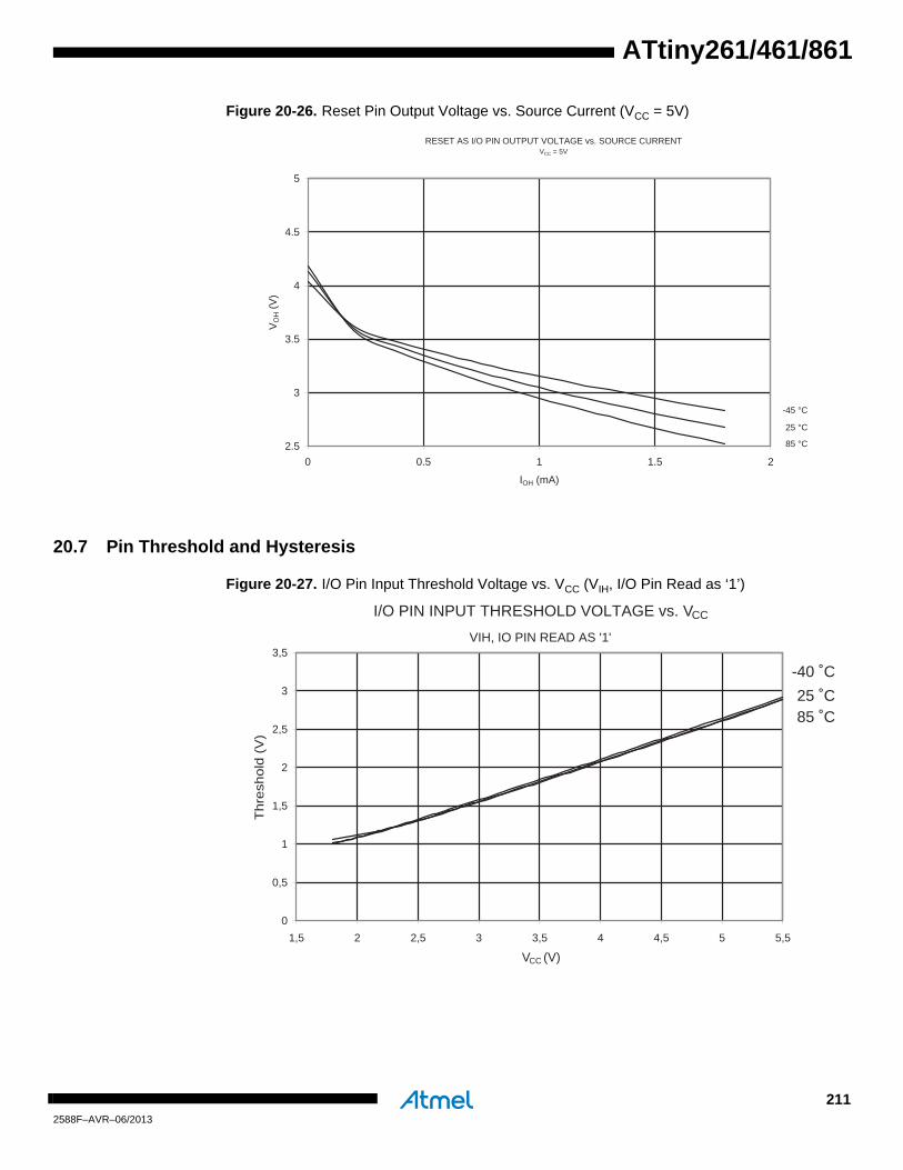
ATtiny261/461/861
Figure 20-26. Reset Pin Output Voltage vs. Source Current (VCC = 5V)
20.7 Pin Threshold and Hysteresis
Figure 20-27. I/O Pin Input Threshold Voltage vs. VCC (VIH, I/O Pin Read as ‘1’)
RESET AS I/O PIN OUTPUT VOLTAGE vs. SOURCE CURRENTVCC = 5V
-45 °C
25 °C
85 °C2.5
3
3.5
4
4.5
5
0 0.5 1 1.5 2
IOH (mA)
VO
H (
V)
I/O PIN INPUT THRESHOLD VOLTAGE vs. VCC
VIH, IO PIN READ AS '1'
85 ˚C25 ˚C
-40 ˚C
0
0,5
1
1,5
2
2,5
3
3,5
1,5 2 2,5 3 3,5 4 4,5 5 5,5
VCC (V)
Th
resh
old
(V
)
2112588F–AVR–06/2013

Figure 20-28. I/O Pin Input Threshold Voltage vs. VCC (VIL, I/O Pin Read as ‘0’)
Figure 20-29. I/O Pin Input Hysteresis vs. VCC
I/O PIN INPUT THRESHOLD VOLTAGE vs. VCC
VIL, IO PIN READ AS '0'
85 ˚C
25 ˚C
-40 ˚C
0
0,5
1
1,5
2
2,5
3
1,5 2 2,5 3 3,5 4 4,5 5 5,5
VCC (V)
Th
resh
old
(V
)
I/O PIN INPUT HYSTERESIS vs. VCC
85 °C25 °C
-40 °C
0
0,1
0,2
0,3
0,4
0,5
0,6
0,7
1,5 2 2,5 3 3,5 4 4,5 5 5,5
VCC (V)
Inp
ut H
yste
resi
s (V
)
2122588F–AVR–06/2013
ATtiny261/461/861
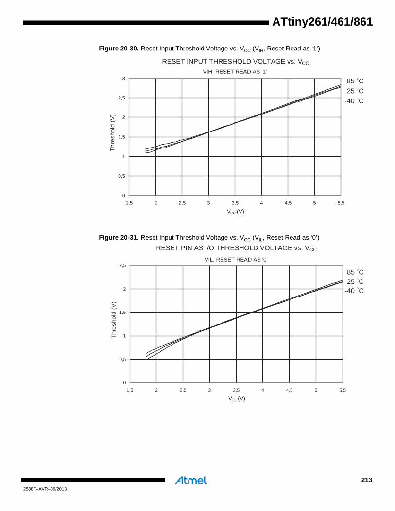
ATtiny261/461/861
Figure 20-30. Reset Input Threshold Voltage vs. VCC (VIH, Reset Read as ‘1’)
Figure 20-31. Reset Input Threshold Voltage vs. VCC (VIL, Reset Read as ‘0’)
RESET INPUT THRESHOLD VOLTAGE vs. VCC
VIH, RESET READ AS '1'
85 ˚C
25 ˚C
-40 ˚C
0
0,5
1
1,5
2
2,5
3
1,5 2 2,5 3 3,5 4 4,5 5 5,5
VCC (V)
Th
resh
old
(V
)
RESET PIN AS I/O THRESHOLD VOLTAGE vs. VCC
VIL, RESET READ AS '0'
85 ˚C25 ˚C
-40 ˚C
0
0,5
1
1,5
2
2,5
1,5 2 2,5 3 3,5 4 4,5 5 5,5
VCC (V)
Th
resh
old
(V
)
2132588F–AVR–06/2013
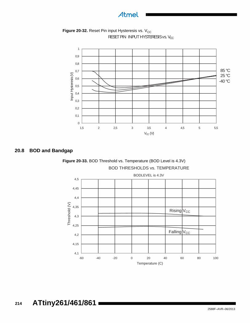
Figure 20-32. Reset Pin input Hysteresis vs. VCC
20.8 BOD and Bandgap
Figure 20-33. BOD Threshold vs. Temperature (BOD Level is 4.3V)
RESET PIN INPUT HYSTERESIS vs. VCC
85 °C25 °C
-40 °C
0
0,1
0,2
0,3
0,4
0,5
0,6
0,7
0,8
0,9
1
1,5 2 2,5 3 3,5 4 4,5 5 5,5
VCC (V)
Inpu
t Hys
tere
sis
(V)
BOD THRESHOLDS vs. TEMPERATURE
BODLEVEL is 4.3V
Rising VCC
Falling VCC
4,1
4,15
4,2
4,25
4,3
4,35
4,4
4,45
4,5
-60 -40 -20 0 20 40 60 80 100
Temperature (C)
Th
resh
old
(V
)
2142588F–AVR–06/2013
ATtiny261/461/861

ATtiny261/461/861
Figure 20-34. BOD Threshold vs. Temperature (BOD Level is 2.7V)
Figure 20-35. BOD Threshold vs. Temperature (BOD Level is 1.8V)
BOD THRESHOLDS vs. TEMPERATURE
BODLEVEL is 2.7V
Falling VCC
Rising VCC
2,5
2,55
2,6
2,65
2,7
2,75
2,8
2,85
2,9
-60 -40 -20 0 20 40 60 80 100
Temperature (C)
Th
resh
old
(V
)
BOD THRESHOLDS vs. TEMPERATURE
BODLEVEL is 1.8V
Rising VCC
Falling VCC
1,6
1,65
1,7
1,75
1,8
1,85
1,9
1,95
2
-60 -40 -20 0 20 40 60 80 100
Temperature (C)
Th
resh
old
(V
)
2152588F–AVR–06/2013

Figure 20-36. Bandgap Voltage vs. Supply Voltage (VCC).
20.9 Internal Oscillator Speed
Figure 20-37. Watchdog Oscillator Frequency vs. VCC
BANDGAP VOLTAGE vs. VCC
85 °C
25 °C
-40 °C
1.04
1.05
1.06
1.07
1.08
1.5 2 2.5 3 3.5 4 4.5 5 5.5
VCC ( V )
Ban
dgap
Vol
tage
( V
)
WATCHDOG OSCILLATOR FREQUENCY vs. VCC
85 ˚C
25 ˚C
-40 ˚C
0,118
0,12
0,122
0,124
0,126
0,128
0,13
0,132
0,134
0,136
0,138
1,5 2 2,5 3 3,5 4 4,5 5 5,5
VCC (V)
F RC (M
Hz)
2162588F–AVR–06/2013
ATtiny261/461/861
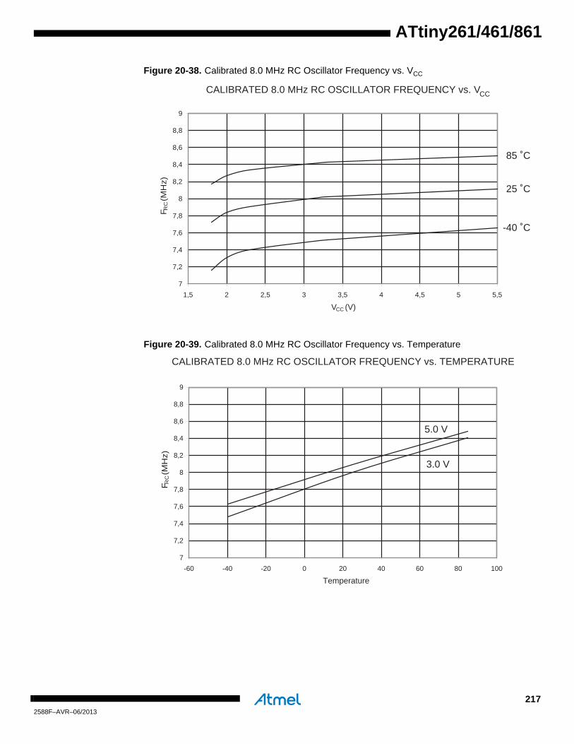
ATtiny261/461/861
Figure 20-38. Calibrated 8.0 MHz RC Oscillator Frequency vs. VCC
Figure 20-39. Calibrated 8.0 MHz RC Oscillator Frequency vs. Temperature
CALIBRATED 8.0 MHz RC OSCILLATOR FREQUENCY vs. VCC
85 ˚C
25 ˚C
-40 ˚C
7
7,2
7,4
7,6
7,8
8
8,2
8,4
8,6
8,8
9
1,5 2 2,5 3 3,5 4 4,5 5 5,5
VCC (V)
F RC (M
Hz)
CALIBRATED 8.0 MHz RC OSCILLATOR FREQUENCY vs. TEMPERATURE
5.0 V
3.0 V
7
7,2
7,4
7,6
7,8
8
8,2
8,4
8,6
8,8
9
-60 -40 -20 0 20 40 60 80 100
Temperature
F RC (M
Hz)
2172588F–AVR–06/2013

Figure 20-40. Calibrated 8.0 MHz RC Oscillator Frequency vs. OSCCAL Value
20.10 Current Consumption of Peripheral Units
Figure 20-41. ADC Current vs. VCC (AREF = AVCC)
CALIBRATED 8.0 MHz RC OSCILLATOR FREQUENCY vs. OSCCAL VALUE
85 ˚C
25 ˚C
-40 ˚C
0
2
4
6
8
10
12
14
16
18
0 16 32 48 64 80 96 112 128 144 160 176 192 208 224 240 256
OSCCAL (X1)
F RC (M
Hz)
ADC CURRENT vs. VCC
AREF = AVCC
0
100
200
300
400
500
600
700
800
900
1000
1,5 2 2,5 3 3,5 4 4,5 5 5,5
VCC (V)
I CC (u
A)
25 ˚C
2182588F–AVR–06/2013
ATtiny261/461/861

ATtiny261/461/861
Figure 20-42. AREF External Reference Current vs. VCC
Figure 20-43. Analog Comparator vs. VCC
AREF EXTERNAL REFERENCE CURRENT vs. VCC
25 ˚C
0
30
60
90
120
150
180
1,5 2 2,5 3 3,5 4 4,5 5 5,5
VCC (V)
I CC (u
A)
ANALOG COMPARATOR vs. VCC
25 ˚C
0
20
40
60
80
100
120
140
160
1,5 2 2,5 3 3,5 4 4,5 5 5,5
VCC (V)
I CC (u
A)
2192588F–AVR–06/2013

Figure 20-44. Brownout Detector Current vs. VCC
Figure 20-45. Programming Current vs. VCC
BROWNOUT DETECTOR CURRENT vs. VCC
85 ˚C
25 ˚C
-40 ˚C
0
5
10
15
20
25
30
1,5 2 2,5 3 3,5 4 4,5 5 5,5
VCC (V)
I CC (u
A)
PROGRAMMING CURRENT vs. VCC
25 ˚C
0
2000
4000
6000
8000
10000
12000
14000
16000
1,5 2 2,5 3 3,5 4 4,5 5 5,5
VCC (V)
I CC (u
A)
2202588F–AVR–06/2013
ATtiny261/461/861

ATtiny261/461/861
Figure 20-46. Watchdog Timer Current vs. VCC
20.11 Current Consumption in Reset and Reset Pulsewidth
Figure 20-47. Reset Supply Current vs. Low Frequency (0.1 - 1.0 MHz, Excluding Current Through the Reset Pull-up)
WATCHDOG TIMER CURRENT vs. VCC
85 ˚C25 ˚C
-40 ˚C
0
1
2
3
4
5
6
7
8
9
10
1,5 2 2,5 3 3,5 4 4,5 5 5,5
VCC (V)
I CC (u
A)
RESET SUPPLY CURRENT vs. Low Frequency
0.1 - 1.0 MHz, EXCLUDING CURRENT THROUGH THE RESET PULL-UP
5.5 V
5.0 V
4.5 V
4.0 V
3.3 V
2.7 V
1.8 V
0
0,02
0,04
0,06
0,08
0,1
0,12
0,14
0 0,1 0,2 0,3 0,4 0,5 0,6 0,7 0,8 0,9 1
Frequency (MHz)
I CC
(mA
)
2212588F–AVR–06/2013

Figure 20-48. Reset Supply Current vs. Frequency (1 - 20 MHz, Excluding Current Through the Reset Pull-up)
Figure 20-49. Minimum Reset Pulse Width vs. VCC
RESET SUPPLY CURRENT vs. VCC
1 - 20 MHz, EXCLUDING CURRENT THROUGH THE RESET PULLUP
5.5 V
5.0 V
4.5 V
0
0,5
1
1,5
2
2,5
0 2 4 6 8 10 12 14 16 18 20
Frequency (MHz)
I CC (m
A)
1.8 V
2.7 V
3.3 V
4.0 V
MINIMUM RESET PULSE WIDTH vs. VCC
85 ˚C25 ˚C
-40 ˚C0
500
1000
1500
2000
2500
1,5 2 2,5 3 3,5 4 4,5 5 5,5
VCC (V)
Pu
lse
wid
th (ns)
2222588F–AVR–06/2013
ATtiny261/461/861

ATtiny261/461/861
21. Register SummaryAddress Name Bit 7 Bit 6 Bit 5 Bit 4 Bit 3 Bit 2 Bit 1 Bit 0 Page
0x3F (0x5F) SREG I T H S V N Z C page 8
0x3E (0x5E) SPH – – – – – SP10 SP9 SP8 page 11
0x3D (0x5D) SPL SP7 SP6 SP5 SP4 SP3 SP2 SP1 SP0 page 11
0x3C (0x5C) Reserved –
0x3B (0x5B) GIMSK INT1 INT0 PCIE1 PCIE0 – – – – page 52
0x3A (0x5A) GIFR INTF1 INTF0 PCIF – – – – – page 53
0x39 (0x59) TIMSK OCIE1D OCIE1A OCIE1B OCIE0A OCIE0B TOIE1 TOIE0 TICIE0 page 86, page 123
0x38 (0x58) TIFR OCF1D OCF1A OCF1B OCF0A OCF0B TOV1 TOV0 ICF0 page 87, page 123
0x37 (0x57) SPMCSR – – – CTPB RFLB PGWRT PGERS SPMEN page 169
0x36 (0x56) PRR PRTIM1 PRTIM0 PRUSI PRADC page 37
0x35 (0x55) MCUCR – PUD SE SM1 SM0 – ISC01 ISC00 page 39, page 69, page 52
0x34 (0x54) MCUSR – – – – WDRF BORF EXTRF PORF page 47,
0x33 (0x53) TCCR0B – – – TSM PSR0 CS02 CS01 CS00 page 85
0x32 (0x52) TCNT0L Timer/Counter0 Counter Register Low Byte page 85
0x31 (0x51) OSCCAL Oscillator Calibration Register page 32
0x30 (0x50) TCCR1A COM1A1 COM1A0 COM1B1 COM1B0 FOC1A FOC1B PWM1A PWM1B page 112
0x2F (0x4F) TCCR1B PWM1X PSR1 DTPS11 DTPS10 CS13 CS12 CS11 CS10 page 169
0x2E (0x4E) TCNT1 Timer/Counter1 Counter Register page 121
0x2D (0x4D) OCR1A Timer/Counter1 Output Compare Register A page 121
0x2C (0x4C) OCR1B Timer/Counter1 Output Compare Register B page 122
0x2B (0x4B) OCR1C Timer/Counter1 Output Compare Register C page 122
0x2A (0x4A) OCR1D Timer/Counter1 Output Compare Register D page 122
0x29 (0x49) PLLCSR LSM PCKE PLLE PLOCK page 120
0x28 (0x48) CLKPR CLKPCE CLKPS3 CLKPS2 CLKPS1 CLKPS0 page 32
0x27 (0x47) TCCR1C COM1A1S COM1A0S COM1B1S COM1B0S COM1D1 COM1D0 FOC1D PWM1D page 117
0x26 (0x46) TCCR1D FPIE1 FPEN1 FPNC1 FPES1 FPAC1 FPF1 WGM11 WGM10 page 118
0x25 (0x45) TC1H TC19 TC18 page 121
0x24 (0x44) DT1 DT1H3 DT1H2 DT1H1 DT1H0 DT1L3 DT1L2 DT1L1 DT1L0 page 124
0x23 (0x43) PCMSK0 PCINT7 PCINT6 PCINT5 PCINT4 PCINT3 PCINT2 PCINT1 PCINT0 page 54
0x22 (0x42) PCMSK1 PCINT15 PCINT14 PCINT13 PCINT12 PCINT11 PCINT10 PCINT9 PCINT8 page 54
0x21 (0x41) WDTCR WDIF WDIE WDP3 WDCE WDE WDP2 WDP1 WDP0 page 47
0x20 (0x40) DWDR DWDR[7:0] page 37
0x1F (0x3F) EEARH EEAR8 page 20
0x1E (0x3E) EEARL EEAR7 EEAR6 EEAR5 EEAR4 EEAR3 EEAR2 EEAR1 EEAR0 page 21
0x1D (0x3D) EEDR EEPROM Data Register page 21
0x1C (0x3C) EECR – – EEPM1 EEPM0 EERIE EEMPE EEPE EERE page 21
0x1B (0x3B) PORTA PORTA7 PORTA6 PORTA5 PORTA4 PORTA3 PORTA2 PORTA1 PORTA0 page 69
0x1A (0x3A) DDRA DDA7 DDA6 DDA5 DDA4 DDA3 DDA2 DDA1 DDA0 page 69
0x19 (0x39) PINA PINA7 PINA6 PINA5 PINA4 PINA3 PINA2 PINA1 PINA0 page 70
0x18 (0x38) PORTB PORTB7 PORTB6 PORTB5 PORTB4 PORTB3 PORTB2 PORTB1 PORTB0 page 70
0x17 (0x37) DDRB DDB7 DDB6 DDB5 DDB4 DDB3 DDB2 DDB1 DDB0 page 70
0x16 (0x36) PINB PINB7 PINB6 PINB5 PINB4 PINB3 PINB2 PINB1 PINB0 page 70
0x15 (0x35) TCCR0A TCW0 ICEN0 ICNC0 ICES0 ACIC0 CTC0 page 84
0x14 (0x34) TCNT0H Timer/Counter0 Counter Register High Byte page 86
0x13 (0x33) OCR0A Timer/Counter0 Output Compare Register A page 86
0x12 (0x32) OCR0B Timer/Counter0 Output Compare Register B page 86
0x11 (0x31) USIPP USIPOS page 136
0x10 (0x30) USIBR USI Buffer Register page 133
0x0F (0x2F) USIDR USI Data Register page 132
0x0E (0x2E) USISR USISIF USIOIF USIPF USIDC USICNT3 USICNT2 USICNT1 USICNT0 page 133
0x0D (0x2D) USICR USISIE USIOIE USIWM1 USIWM0 USICS1 USICS0 USICLK USITC page 134
0x0C (0x2C) GPIOR2 General Purpose I/O Register 2 page 22
0x0B (0x2B) GPIOR1 General Purpose I/O Register 1 page 23
0x0A (0x2A) GPIOR0 General Purpose I/O Register 0 page 23
0x09 (0x29) ACSRB HSEL HLEV ACM2 ACM1 ACM0 page 140
0x08 (0x28) ACSRA ACD ACBG ACO ACI ACIE ACME ACIS1 ACIS0 page 139
0x07 (0x27) ADMUX REFS1 REFS0 ADLAR MUX4 MUX3 MUX2 MUX1 MUX0 page 155
0x06 (0x26) ADCSRA ADEN ADSC ADATE ADIF ADIE ADPS2 ADPS1 ADPS0 page 159
0x05 (0x25) ADCH ADC Data Register High Byte page 160
0x04 (0x24) ADCL ADC Data Register Low Byte page 160
0x03 (0x23) ADCSRB BIN GSEL REFS2 MUX5 ADTS2 ADTS1 ADTS0 page 161
0x02 (0x22) DIDR1 ADC10D ADC9D ADC8D ADC7D page 162
0x01 (0x21) DIDR0 ADC6D ADC5D ADC4D ADC3D AREFD ADC2D ADC1D ADC0D page 162
0x00 (0x20) TCCR1E – - OC1OE5 OC1OE4 OC1OE3 OC1OE2 OC1OE1 OC1OE0 page 119
2232588F–AVR–06/2013

Note: 1. For compatibility with future devices, reserved bits should be written to zero if accessed. Reserved I/O memory addresses should never be written.
2. I/O Registers within the address range 0x00 - 0x1F are directly bit-accessible using the SBI and CBI instructions. In these registers, the value of single bits can be checked by using the SBIS and SBIC instructions.
3. Some of the Status Flags are cleared by writing a logical one to them. Note that, unlike most other AVRs, the CBI and SBI instructions will only operation the specified bit, and can therefore be used on registers containing such Status Flags. The CBI and SBI instructions work with registers 0x00 to 0x1F only.
2242588F–AVR–06/2013
ATtiny261/461/861

ATtiny261/461/861
22. Instruction Set SummaryMnemonics Operands Description Operation Flags #Clocks
ARITHMETIC AND LOGIC INSTRUCTIONS
ADD Rd, Rr Add two Registers Rd Rd + Rr Z,C,N,V,H 1
ADC Rd, Rr Add with Carry two Registers Rd Rd + Rr + C Z,C,N,V,H 1
ADIW Rdl,K Add Immediate to Word Rdh:Rdl Rdh:Rdl + K Z,C,N,V,S 2
SUB Rd, Rr Subtract two Registers Rd Rd - Rr Z,C,N,V,H 1
SUBI Rd, K Subtract Constant from Register Rd Rd - K Z,C,N,V,H 1
SBC Rd, Rr Subtract with Carry two Registers Rd Rd - Rr - C Z,C,N,V,H 1
SBCI Rd, K Subtract with Carry Constant from Reg. Rd Rd - K - C Z,C,N,V,H 1
SBIW Rdl,K Subtract Immediate from Word Rdh:Rdl Rdh:Rdl - K Z,C,N,V,S 2
AND Rd, Rr Logical AND Registers Rd Rd Rr Z,N,V 1
ANDI Rd, K Logical AND Register and Constant Rd Rd K Z,N,V 1
OR Rd, Rr Logical OR Registers Rd Rd v Rr Z,N,V 1
ORI Rd, K Logical OR Register and Constant Rd Rd v K Z,N,V 1
EOR Rd, Rr Exclusive OR Registers Rd Rd Rr Z,N,V 1
COM Rd One’s Complement Rd 0xFF Rd Z,C,N,V 1
NEG Rd Two’s Complement Rd 0x00 Rd Z,C,N,V,H 1
SBR Rd,K Set Bit(s) in Register Rd Rd v K Z,N,V 1
CBR Rd,K Clear Bit(s) in Register Rd Rd (0xFF - K) Z,N,V 1
INC Rd Increment Rd Rd + 1 Z,N,V 1
DEC Rd Decrement Rd Rd 1 Z,N,V 1
TST Rd Test for Zero or Minus Rd Rd Rd Z,N,V 1
CLR Rd Clear Register Rd Rd Rd Z,N,V 1
SER Rd Set Register Rd 0xFF None 1
BRANCH INSTRUCTIONS
RJMP k Relative Jump PC PC + k + 1 None 2
IJMP Indirect Jump to (Z) PC Z None 2
RCALL k Relative Subroutine Call PC PC + k + 1 None 3
ICALL Indirect Call to (Z) PC Z None 3
RET Subroutine Return PC STACK None 4
RETI Interrupt Return PC STACK I 4
CPSE Rd,Rr Compare, Skip if Equal if (Rd = Rr) PC PC + 2 or 3 None 1/2/3
CP Rd,Rr Compare Rd Rr Z, N,V,C,H 1
CPC Rd,Rr Compare with Carry Rd Rr C Z, N,V,C,H 1
CPI Rd,K Compare Register with Immediate Rd K Z, N,V,C,H 1
SBRC Rr, b Skip if Bit in Register Cleared if (Rr(b)=0) PC PC + 2 or 3 None 1/2/3
SBRS Rr, b Skip if Bit in Register is Set if (Rr(b)=1) PC PC + 2 or 3 None 1/2/3
SBIC P, b Skip if Bit in I/O Register Cleared if (P(b)=0) PC PC + 2 or 3 None 1/2/3
SBIS P, b Skip if Bit in I/O Register is Set if (P(b)=1) PC PC + 2 or 3 None 1/2/3
BRBS s, k Branch if Status Flag Set if (SREG(s) = 1) then PCPC+k + 1 None 1/2
BRBC s, k Branch if Status Flag Cleared if (SREG(s) = 0) then PCPC+k + 1 None 1/2
BREQ k Branch if Equal if (Z = 1) then PC PC + k + 1 None 1/2
BRNE k Branch if Not Equal if (Z = 0) then PC PC + k + 1 None 1/2
BRCS k Branch if Carry Set if (C = 1) then PC PC + k + 1 None 1/2
BRCC k Branch if Carry Cleared if (C = 0) then PC PC + k + 1 None 1/2
BRSH k Branch if Same or Higher if (C = 0) then PC PC + k + 1 None 1/2
BRLO k Branch if Lower if (C = 1) then PC PC + k + 1 None 1/2
BRMI k Branch if Minus if (N = 1) then PC PC + k + 1 None 1/2
BRPL k Branch if Plus if (N = 0) then PC PC + k + 1 None 1/2
BRGE k Branch if Greater or Equal, Signed if (N V= 0) then PC PC + k + 1 None 1/2
BRLT k Branch if Less Than Zero, Signed if (N V= 1) then PC PC + k + 1 None 1/2
BRHS k Branch if Half Carry Flag Set if (H = 1) then PC PC + k + 1 None 1/2
BRHC k Branch if Half Carry Flag Cleared if (H = 0) then PC PC + k + 1 None 1/2
BRTS k Branch if T Flag Set if (T = 1) then PC PC + k + 1 None 1/2
BRTC k Branch if T Flag Cleared if (T = 0) then PC PC + k + 1 None 1/2
BRVS k Branch if Overflow Flag is Set if (V = 1) then PC PC + k + 1 None 1/2
BRVC k Branch if Overflow Flag is Cleared if (V = 0) then PC PC + k + 1 None 1/2
BRIE k Branch if Interrupt Enabled if ( I = 1) then PC PC + k + 1 None 1/2
BRID k Branch if Interrupt Disabled if ( I = 0) then PC PC + k + 1 None 1/2
BIT AND BIT-TEST INSTRUCTIONS
SBI P,b Set Bit in I/O Register I/O(P,b) 1 None 2
CBI P,b Clear Bit in I/O Register I/O(P,b) 0 None 2
LSL Rd Logical Shift Left Rd(n+1) Rd(n), Rd(0) 0 Z,C,N,V 1
LSR Rd Logical Shift Right Rd(n) Rd(n+1), Rd(7) 0 Z,C,N,V 1
ROL Rd Rotate Left Through Carry Rd(0)C,Rd(n+1) Rd(n),CRd(7) Z,C,N,V 1
ROR Rd Rotate Right Through Carry Rd(7)C,Rd(n) Rd(n+1),CRd(0) Z,C,N,V 1
2252588F–AVR–06/2013

ASR Rd Arithmetic Shift Right Rd(n) Rd(n+1), n=0..6 Z,C,N,V 1
SWAP Rd Swap Nibbles Rd(3..0)Rd(7..4),Rd(7..4)Rd(3..0) None 1
BSET s Flag Set SREG(s) 1 SREG(s) 1
BCLR s Flag Clear SREG(s) 0 SREG(s) 1
BST Rr, b Bit Store from Register to T T Rr(b) T 1
BLD Rd, b Bit load from T to Register Rd(b) T None 1
SEC Set Carry C 1 C 1
CLC Clear Carry C 0 C 1
SEN Set Negative Flag N 1 N 1
CLN Clear Negative Flag N 0 N 1
SEZ Set Zero Flag Z 1 Z 1
CLZ Clear Zero Flag Z 0 Z 1
SEI Global Interrupt Enable I 1 I 1
CLI Global Interrupt Disable I 0 I 1
SES Set Signed Test Flag S 1 S 1
CLS Clear Signed Test Flag S 0 S 1
SEV Set Twos Complement Overflow. V 1 V 1
CLV Clear Twos Complement Overflow V 0 V 1
SET Set T in SREG T 1 T 1
CLT Clear T in SREG T 0 T 1
SEH Set Half Carry Flag in SREG H 1 H 1
CLH Clear Half Carry Flag in SREG H 0 H 1
DATA TRANSFER INSTRUCTIONS
MOV Rd, Rr Move Between Registers Rd Rr None 1
MOVW Rd, Rr Copy Register Word Rd+1:Rd Rr+1:Rr None 1
LDI Rd, K Load Immediate Rd K None 1
LD Rd, X Load Indirect Rd (X) None 2
LD Rd, X+ Load Indirect and Post-Inc. Rd (X), X X + 1 None 2
LD Rd, - X Load Indirect and Pre-Dec. X X - 1, Rd (X) None 2
LD Rd, Y Load Indirect Rd (Y) None 2
LD Rd, Y+ Load Indirect and Post-Inc. Rd (Y), Y Y + 1 None 2
LD Rd, - Y Load Indirect and Pre-Dec. Y Y - 1, Rd (Y) None 2
LDD Rd,Y+q Load Indirect with Displacement Rd (Y + q) None 2
LD Rd, Z Load Indirect Rd (Z) None 2
LD Rd, Z+ Load Indirect and Post-Inc. Rd (Z), Z Z+1 None 2
LD Rd, -Z Load Indirect and Pre-Dec. Z Z - 1, Rd (Z) None 2
LDD Rd, Z+q Load Indirect with Displacement Rd (Z + q) None 2
LDS Rd, k Load Direct from SRAM Rd (k) None 2
ST X, Rr Store Indirect (X) Rr None 2
ST X+, Rr Store Indirect and Post-Inc. (X) Rr, X X + 1 None 2
ST - X, Rr Store Indirect and Pre-Dec. X X - 1, (X) Rr None 2
ST Y, Rr Store Indirect (Y) Rr None 2
ST Y+, Rr Store Indirect and Post-Inc. (Y) Rr, Y Y + 1 None 2
ST - Y, Rr Store Indirect and Pre-Dec. Y Y - 1, (Y) Rr None 2
STD Y+q,Rr Store Indirect with Displacement (Y + q) Rr None 2
ST Z, Rr Store Indirect (Z) Rr None 2
ST Z+, Rr Store Indirect and Post-Inc. (Z) Rr, Z Z + 1 None 2
ST -Z, Rr Store Indirect and Pre-Dec. Z Z - 1, (Z) Rr None 2
STD Z+q,Rr Store Indirect with Displacement (Z + q) Rr None 2
STS k, Rr Store Direct to SRAM (k) Rr None 2
LPM Load Program Memory R0 (Z) None 3
LPM Rd, Z Load Program Memory Rd (Z) None 3
LPM Rd, Z+ Load Program Memory and Post-Inc Rd (Z), Z Z+1 None 3
SPM Store Program Memory (z) R1:R0 None
IN Rd, P In Port Rd P None 1
OUT P, Rr Out Port P Rr None 1
PUSH Rr Push Register on Stack STACK Rr None 2
POP Rd Pop Register from Stack Rd STACK None 2
MCU CONTROL INSTRUCTIONS
NOP No Operation None 1
SLEEP Sleep (see specific descr. for Sleep function) None 1
WDR Watchdog Reset (see specific descr. for WDR/Timer) None 1
BREAK Break For On-chip Debug Only None N/A
Mnemonics Operands Description Operation Flags #Clocks
2262588F–AVR–06/2013
ATtiny261/461/861

ATtiny261/461/861
23. Ordering Information
Notes: 1. These devices can also be supplied in wafer form. Please contact your local Atmel sales office for detailed ordering informa-tion and minimum quantities.
2. All packages are Pb-free, halide-free and fully green and they comply with the European directive for Restriction of Hazard-ous Substances (RoHS).
3. For Speed vs. VCC, see Figure 19.3 on page 188.
4. Code indicators:
– U: matte tin
– R: tape & reel
5. Mature devices, replaced by ATtiny261A.
23.1 ATtiny261 - Mature
Speed (MHz)(3) Power Supply (V) Ordering Code(4)(5) Package(2) Operational Range
10 1.8 - 5.5
ATtiny261V-10MUATtiny261V-10MURATtiny261V-10PUATtiny261V-10SUATtiny261V-10SUR
32M1-A32M1-A20P320S220S2
Industrial(-40C to +85C)(1)
20 2.7 - 5.5
ATtiny261-20MUATtiny261-20MURATtiny261-20PUATtiny261-20SUATtiny261-20SUR
32M1-A32M1-A20P320S220S2
Industrial(-40C to +85C)(1)
2272588F–AVR–06/2013

Package Type
32M1-A 32-pad, 5 x 5 x 1.0 mm Body, Lead Pitch 0.50 mm, Micro Lead Frame Package (MLF)
20P3 20-lead, 0.300" Wide, Plastic Dual Inline Package (PDIP)
20S2 20-lead, 0.300" Wide, Plastic Gull Wing Smal Outline Package (SOIC)
2282588F–AVR–06/2013
ATtiny261/461/861
ATtiny261/461/861
Notes: 1. These devices can also be supplied in wafer form. Please contact your local Atmel sales office for detailed ordering informa-tion and minimum quantities.
2. All packages are Pb-free, halide-free and fully green and they comply with the European directive for Restriction of Hazard-ous Substances (RoHS).
3. For Speed vs. VCC, see Figure 19.3 on page 188.
4. Code indicators:
– U: matte tin
– R: tape & reel
23.2 ATtiny461
Speed (MHz)(3) Power Supply (V) Ordering Code(4) Package(2) Operational Range
10 1.8 - 5.5
ATtiny461V-10MUATtiny461V-10MURATtiny461V-10PUATtiny461V-10SUATtiny461V-10SUR
32M1-A32M1-A20P320S220S2
Industrial(-40C to +85C)(1)
20 2.7 - 5.5
ATtiny461-20MUATtiny461-20MURATtiny461-20PUATtiny461-20SUATtiny461-20SUR
32M1-A32M1-A20P320S220S2
Industrial(-40C to +85C)(1)
Package Type
32M1-A 32-pad, 5 x 5 x 1.0 mm Body, Lead Pitch 0.50 mm, Micro Lead Frame Package (MLF)
20P3 20-lead, 0.300" Wide, Plastic Dual Inline Package (PDIP)
20S2 20-lead, 0.300" Wide, Plastic Gull Wing Smal Outline Package (SOIC)
2292588F–AVR–06/2013

Notes: 1. These devices can also be supplied in wafer form. Please contact your local Atmel sales office for detailed ordering informa-tion and minimum quantities.
2. All packages are Pb-free, halide-free and fully green and they comply with the European directive for Restriction of Hazard-ous Substances (RoHS).
3. For Speed vs. VCC, see Figure 19.3 on page 188.
4. Code indicators:
– U: matte tin
– R: tape & reel
23.3 ATtiny861
Speed (MHz)(3) Power Supply (V) Ordering Code(4) Package(2) Operational Range
10 1.8 - 5.5
ATtiny861V-10MUATtiny861V-10MURATtiny861V-10PUATtiny861V-10SUATtiny861V-10SUR
32M1-A32M1-A20P320S220S2
Industrial(-40C to +85C)(1)
20 2.7 - 5.5
ATtiny861-20MUATtiny861-20MURATtiny861-20PUATtiny861-20SUATtiny861-20SUR
32M1-A32M1-A20P320S220S2
Industrial(-40C to +85C)(1)
Package Type
32M1-A 32-pad, 5 x 5 x 1.0 mm Body, Lead Pitch 0.50 mm, Micro Lead Frame Package (MLF)
20P3 20-lead, 0.300" Wide, Plastic Dual Inline Package (PDIP)
20S2 20-lead, 0.300" Wide, Plastic Gull Wing Smal Outline Package (SOIC)
2302588F–AVR–06/2013
ATtiny261/461/861

ATtiny261/461/861
24. Packaging Information
24.1 32M1-A
2325 Orchard Parkway San Jose, CA 95131
TITLE DRAWING NO.
R
REV. 32M1-A, 32-pad, 5 x 5 x 1.0 mm Body, Lead Pitch 0.50 mm, D32M1-A
8/19/04
3.10 mm Exposed Pad, Micro Lead Frame Package (MLF)
COMMON DIMENSIONS(Unit of Measure = mm)
SYMBOL MIN NOM MAX NOTE
D1
D
E1 E
eb
A3A2
A1 A
D2
E2
0.08 C
L
1
2
3
P
P
01
2
3
A 0.80 0.90 1.00
A1 – 0.02 0.05
A2 – 0.65 1.00
A3 0.20 REF
b 0.18 0.23 0.30
D 5.00 BSC
D1 4.75 BSC
D2 2.95 3.10 3.25
E 5.00 BSC
E1 4.75BSC
E2 2.95 3.10 3.25
e 0.50 BSC
L 0.30 0.40 0.50
P – – 0.60
– – 12o
Note: JEDEC Standard MO-220, Fig. 2 (Anvil Singulation), VHHD-2.
TOP VIEW
SIDE VIEW
BOTTOM VIEW
0
Pin 1 ID
Pin #1 Notch (0.20 R)
K 0.20 – –
K
K
2312588F–AVR–06/2013

24.2 20P3
2322588F–AVR–06/2013
ATtiny261/461/861

ATtiny261/461/861
24.3 20S2
2332588F–AVR–06/2013

25. Errata
25.1 Errata ATtiny261The revision letter in this section refers to the revision of the ATtiny261 device.
25.1.1 Rev A
No known errata.
25.2 Errata ATtiny461The revision letter in this section refers to the revision of the ATtiny461 device.
25.2.1 Rev B
Yield improvement. No known errata.
25.2.2 Rev A
No known errata.
25.3 Errata ATtiny861The revision letter in this section refers to the revision of the ATtiny861 device.
25.3.1 Rev B
No known errata.
25.3.2 Rev A
Not sampled.
2342588F–AVR–06/2013
ATtiny261/461/861

ATtiny261/461/861
26. Datasheet Revision HistoryPlease note that the referring page numbers in this section refer to the complete document.
26.1 Rev. 2588F – 06/131. ATtiny261 changed status to “Mature”.
26.2 Rev. 2588E – 08/101. Added tape and reel in “Ordering Information” on page 227.
2. Clarified Section 6.4 “Clock Output Buffer” on page 32.
3. Removed text "Not recommended for new designs" from cover page.
26.3 Rev. 2588D – 06/101. Removed “Preliminary” from cover page.
2. Added clarification before Table 6-10, “Capacitance for Low-Frequency Crystal Oscilla-tor,” on page 29.
3. Updated Figure 15-1 “Analog to Digital Converter Block Schematic” on page 143, changed INTERNAL 1.18V REFERENCE to 1.1V.
4. Updated Table 18-8, “No. of Words in a Page and No. of Pages in the EEPROM,” on page 173, No. of Pages from 64 to 32 for ATtiny261.
5. Adjusted notes in Table 19-1, “DC Characteristics. TA = -40°C to +85°C, VCC = 1.8V to 5.5V (unless otherwise noted).,” on page 187.
26.4 Rev. 2588C – 10/091. Updated document template. Re-arranged some sections.
2. Changed device status to "Not Recommended for New Designs".
3. Added Sections:
– “Data Retention” on page 6
– “Clock Sources” on page 25
– “Low Level Interrupt” on page 51
– “Prescaling and Conversion Timing” on page 145
– “Clock speed considerations” on page 131
4. Updated Sections:
– “Code Examples” on page 6
– “High-Frequency PLL Clock” on page 26
– “Normal Mode” on page 99
– “Features” on page 142
– “Temperature Measurement” on page 154
– “Limitations of debugWIRE” on page 164
– Step 1. on page 174
– “Programming the Flash” on page 180
– “System and Reset Characteristics” on page 190
5. Added Figures:
– “Flash Programming Waveforms” on page 182
2352588F–AVR–06/2013

– “Reset Pin Output Voltage vs. Sink Current (VCC = 3V)” on page 209
– “Reset Pin Output Voltage vs. Sink Current (VCC = 3V)” on page 209
– “Reset Pin Output Voltage vs. Sink Current (VCC = 3V)” on page 209
– “Reset Pin Output Voltage vs. Sink Current (VCC = 3V)” on page 209
– “Bandgap Voltage vs. Supply Voltage (VCC).” on page 216
6. Updated Figures:
– “Block Diagram” on page 4
– “Clock Distribution” on page 24
7. Added Table:
– “Capacitance for Low-Frequency Crystal Oscillator” on page 29
8. Updated Tables:
– “Start-up Times for the Internal Calibrated RC Oscillator Clock Selection” on page 28
– “Start-up Times for the 128 kHz Internal Oscillator” on page 29
– “Active Clock Domains and Wake-up Sources in Different Sleep Modes” on page 36
– “Serial Programming Characteristics, TA = -40°C to +85°C, VCC = 1.8 - 5.5V (Unless Otherwise Noted)” on page 193
9. Updated Register Descriptions:
– “TCCR1A – Timer/Counter1 Control Register A” on page 112
– “TCCR1C – Timer/Counter1 Control Register C” on page 117
– “ADMUX – ADC Multiplexer Selection Register” on page 155
10. Updated assembly program example in section “Write” on page 17.
11. Updated “DC Characteristics. TA = -40°C to +85°C, VCC = 1.8V to 5.5V (unless other-wise noted).” on page 187.
26.5 Rev. 2588B – 11/061. Updated “Ordering Information” on page 227.
2. Updated “Packaging Information” on page 231.
26.6 Rev. 2588A – 10/061. Initial Revision.
2362588F–AVR–06/2013
ATtiny261/461/861
ATtiny261/461/861
Table of Contents
Features ..................................................................................................... 1
1 Pin Configurations ................................................................................... 2
1.1 Pin Descriptions .................................................................................................3
2 Overview ................................................................................................... 4
2.1 Block Diagram ...................................................................................................4
3 About ......................................................................................................... 6
3.1 Resources .........................................................................................................6
3.2 Code Examples .................................................................................................6
3.3 Data Retention ...................................................................................................6
3.4 Disclaimer ..........................................................................................................6
4 CPU Core .................................................................................................. 7
4.1 Architectural Overview .......................................................................................7
4.2 ALU – Arithmetic Logic Unit ...............................................................................8
4.3 Status Register ..................................................................................................8
4.4 General Purpose Register File ........................................................................10
4.5 Stack Pointer ...................................................................................................11
4.6 Instruction Execution Timing ...........................................................................11
4.7 Reset and Interrupt Handling ...........................................................................12
5 Memories ................................................................................................ 15
5.1 In-System Re-programmable Flash Program Memory ....................................15
5.2 SRAM Data Memory ........................................................................................15
5.3 EEPROM Data Memory ..................................................................................16
5.4 I/O Memory ......................................................................................................20
5.5 Register Description ........................................................................................20
6 Clock System ......................................................................................... 24
6.1 Clock Subsystems ...........................................................................................24
6.2 Clock Sources .................................................................................................25
6.3 System Clock Prescaler ..................................................................................31
6.4 Clock Output Buffer .........................................................................................32
6.5 Register Description ........................................................................................32
7 Power Management and Sleep Modes ................................................. 36
7.1 Sleep Modes ....................................................................................................36
i2588F–AVR–06/2013

7.2 Power Reduction Register ...............................................................................37
7.3 Minimizing Power Consumption ......................................................................37
7.4 Register Description ........................................................................................39
8 System Control and Reset .................................................................... 41
8.1 Reset Sources .................................................................................................42
8.2 Internal Voltage Reference ..............................................................................44
8.3 Watchdog Timer ..............................................................................................44
8.4 Register Description ........................................................................................47
9 Interrupts ................................................................................................ 50
9.1 Interrupt Vectors ..............................................................................................50
9.2 External Interrupts ...........................................................................................51
9.3 Register Description ........................................................................................52
10 I/O Ports .................................................................................................. 55
10.1 Ports as General Digital I/O .............................................................................56
10.2 Alternate Port Functions ..................................................................................60
10.3 Register Description ........................................................................................69
11 Timer/Counter0 ...................................................................................... 71
11.1 Features ..........................................................................................................71
11.2 Overview ..........................................................................................................71
11.3 Clock Sources .................................................................................................72
11.4 Counter Unit ....................................................................................................74
11.5 Input Capture Unit ...........................................................................................75
11.6 Output Compare Unit .......................................................................................76
11.7 Modes of Operation .........................................................................................77
11.8 Timer/Counter Timing Diagrams .....................................................................79
11.9 Accessing Registers in 16-bit Mode ................................................................80
11.10 Register Description ........................................................................................84
12 Timer/Counter1 ...................................................................................... 89
12.1 Features ..........................................................................................................89
12.2 Overview ..........................................................................................................89
12.3 Clock Sources .................................................................................................92
12.4 Counter Unit ....................................................................................................93
12.5 Output Compare Unit .......................................................................................94
12.6 Dead Time Generator ......................................................................................96
ii2588F–AVR–06/2013
ATtiny261/461/861

ATtiny261/461/861
12.7 Compare Match Output Unit ............................................................................97
12.8 Modes of Operation .........................................................................................99
12.9 Timer/Counter Timing Diagrams ...................................................................106
12.10 Fault Protection Unit ......................................................................................107
12.11 Accessing 10-Bit Registers ............................................................................108
12.12 Register Description ......................................................................................112
13 USI – Universal Serial Interface .......................................................... 125
13.1 Features ........................................................................................................125
13.2 Overview ........................................................................................................125
13.3 Functional Descriptions .................................................................................126
13.4 Alternative USI Usage ...................................................................................132
13.5 Register Descriptions ....................................................................................132
14 AC – Analog Comparator .................................................................... 137
14.1 Analog Comparator Multiplexed Input ...........................................................137
14.2 Register Description ......................................................................................139
15 ADC – Analog to Digital Converter ..................................................... 142
15.1 Features ........................................................................................................142
15.2 Overview ........................................................................................................142
15.3 Operation .......................................................................................................143
15.4 Starting a Conversion ....................................................................................144
15.5 Prescaling and Conversion Timing ................................................................145
15.6 Changing Channel or Reference Selection ...................................................148
15.7 ADC Noise Canceler .....................................................................................149
15.8 Analog Input Circuitry ....................................................................................150
15.9 Noise Canceling Techniques .........................................................................150
15.10 ADC Accuracy Definitions .............................................................................151
15.11 ADC Conversion Result .................................................................................153
15.12 Temperature Measurement ...........................................................................154
15.13 Register Description ......................................................................................155
16 debugWIRE On-chip Debug System .................................................. 163
16.1 Features ........................................................................................................163
16.2 Overview ........................................................................................................163
16.3 Physical Interface ..........................................................................................163
16.4 Software Break Points ...................................................................................164
16.5 Limitations of debugWIRE .............................................................................164
iii2588F–AVR–06/2013

16.6 Register Description ......................................................................................164
17 Self-Programming the Flash ............................................................... 165
17.1 Performing Page Erase by SPM ....................................................................165
17.2 Filling the Temporary Buffer (Page Loading) .................................................165
17.3 Performing a Page Write ...............................................................................166
17.4 Addressing the Flash During Self-Programming ...........................................166
17.5 EEPROM Write Prevents Writing to SPMCSR ..............................................167
17.6 Reading Fuse and Lock Bits from Software ..................................................167
17.7 Preventing Flash Corruption ..........................................................................168
17.8 Programming Time for Flash when Using SPM ............................................168
17.9 Register Description ......................................................................................169
18 Memory Programming ......................................................................... 170
18.1 Program And Data Memory Lock Bits ...........................................................170
18.2 Fuse Bytes .....................................................................................................171
18.3 Signature Bytes .............................................................................................172
18.4 Calibration Byte .............................................................................................173
18.5 Page Size ......................................................................................................173
18.6 Serial Programming .......................................................................................173
18.7 Parallel Programming ....................................................................................177
19 Electrical Characteristics .................................................................... 187
19.1 Absolute Maximum Ratings* .........................................................................187
19.2 DC Characteristics .........................................................................................187
19.3 Speed ............................................................................................................188
19.4 Clock Characteristics .....................................................................................189
19.5 System and Reset Characteristics ................................................................190
19.6 ADC Characteristics ......................................................................................192
19.7 Serial Programming Characteristics ..............................................................193
19.8 Parallel Programming Characteristics ...........................................................194
20 Typical Characteristics ........................................................................ 197
20.1 Supply Current of I/O modules ......................................................................197
20.2 Active Supply Current ....................................................................................198
20.3 Idle Supply Current ........................................................................................201
20.4 Power-down Supply Current ..........................................................................203
20.5 Pin Pull-up .....................................................................................................204
20.6 Pin Driver Strength ........................................................................................207
iv2588F–AVR–06/2013
ATtiny261/461/861

ATtiny261/461/861
20.7 Pin Threshold and Hysteresis ........................................................................211
20.8 BOD and Bandgap ........................................................................................214
20.9 Internal Oscillator Speed ...............................................................................216
20.10 Current Consumption of Peripheral Units ......................................................218
20.11 Current Consumption in Reset and Reset Pulsewidth ..................................221
21 Register Summary ............................................................................... 223
22 Instruction Set Summary .................................................................... 225
23 Ordering Information ........................................................................... 227
23.1 ATtiny261 - Mature ........................................................................................227
23.2 ATtiny461 ......................................................................................................229
23.3 ATtiny861 ......................................................................................................230
24 Packaging Information ........................................................................ 231
24.1 32M1-A ..........................................................................................................231
24.2 20P3 ..............................................................................................................232
24.3 20S2 ..............................................................................................................233
25 Errata ..................................................................................................... 234
25.1 Errata ATtiny261 ............................................................................................234
25.2 Errata ATtiny461 ............................................................................................234
25.3 Errata ATtiny861 ............................................................................................234
26 Datasheet Revision History ................................................................ 235
26.1 Rev. 2588F – 06/13 .......................................................................................235
26.2 Rev. 2588E – 08/10 .......................................................................................235
26.3 Rev. 2588D – 06/10 .......................................................................................235
26.4 Rev. 2588C – 10/09 .......................................................................................235
26.5 Rev. 2588B – 11/06 .......................................................................................236
26.6 Rev. 2588A – 10/06 .......................................................................................236
Table of Contents....................................................................................... i
v2588F–AVR–06/2013

Atmel Corporation
1600 Technology Drive
San Jose, CA 95110
USA
Tel: (+1) (408) 441-0311
Fax: (+1) (408) 487-2600
www.atmel.com
Atmel Asia Limited
Unit 01-5 & 16, 19F
BEA Tower, Millennium City 5
418 Kwun Tong Roa
Kwun Tong, Kowloon
HONG KONG
Tel: (+852) 2245-6100
Fax: (+852) 2722-1369
Atmel Munich GmbH
Business Campus
Parkring 4
D-85748 Garching b. Munich
GERMANY
Tel: (+49) 89-31970-0
Fax: (+49) 89-3194621
Atmel Japan G.K.
16F Shin-Osaki Kangyo Bldg
1-6-4 Osaki, Shinagawa-ku
Tokyo 141-0032
JAPAN
Tel: (+81) (3) 6417-0300
Fax: (+81) (3) 6417-0370
© 2013 Atmel Corporation. All rights reserved. / Rev.: 2588F–AVR–06/2013
Disclaimer: The information in this document is provided in connection with Atmel products. No license, express or implied, by estoppel or otherwise, to any intellectual property right is granted by this document or in connection with the sale of Atmel products. EXCEPT AS SET FORTH IN THE ATMEL TERMS AND CONDITIONS OF SALES LOCATED ON THE ATMEL WEBSITE, ATMEL ASSUMES NO LIABILITY WHATSOEVER AND DISCLAIMS ANY EXPRESS, IMPLIED OR STATUTORY WARRANTY RELATING TO ITS PRODUCTS INCLUDING, BUT NOT LIMITED TO, THE IMPLIED WARRANTY OF MERCHANTABILITY, FITNESS FOR A PARTICULAR PURPOSE, OR NON-INFRINGEMENT. IN NO EVENT SHALL ATMEL BE LIABLE FOR ANY DIRECT, INDIRECT, CONSEQUENTIAL, PUNITIVE, SPECIAL OR INCIDENTAL DAMAGES (INCLUDING, WITHOUT LIMITATION, DAMAGES FOR LOSS AND PROFITS, BUSINESS INTERRUPTION, OR LOSS OF INFORMATION) ARISING OUT OF THE USE OR INABILITY TO USE THIS DOCUMENT, EVEN IF ATMEL HAS BEEN ADVISED OF THE POSSIBILITY OF SUCH DAMAGES. Atmel makes no representations or warranties with respect to the accuracy or completeness of the contents of this document and reserves the right to make changes to specifications and products descriptions at any time without notice. Atmel does not make any commitment to update the information contained herein. Unless specifically provided otherwise, Atmel products are not suitable for, and shall not be used in,
Atmel®, Atmel logo and combinations thereof, Enabling Unlimited Possibilities®, AVR® and others are registered trademarks or trademarks of Atmel Corporation or its subsidiaries. Other terms and product names may be trademarks of others.
2588F–AVR–06/2013
automotive applications. Atmel products are not intended, authorized, or warranted for use as components in applications intended to support or sustain life.