8051 core specification. outlines introduction introduction architecture architecture operation...
TRANSCRIPT
8051 Core 8051 Core SpecificationSpecification
OutlinesOutlines
IntroductionIntroduction ArchitectureArchitecture OperationOperation RegistersRegisters
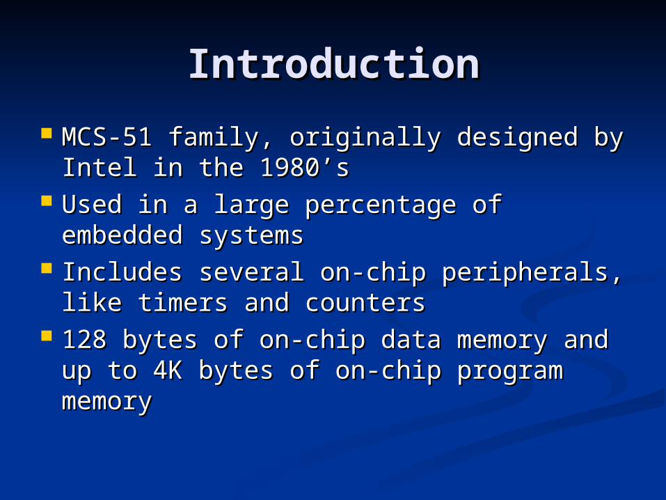
IntroductionIntroduction
MCS-51 family, originally designed by MCS-51 family, originally designed by Intel in the 1980’sIntel in the 1980’s
Used in a large percentage of Used in a large percentage of embedded systemsembedded systems
Includes several on-chip peripherals, Includes several on-chip peripherals, like timers and counterslike timers and counters
128 bytes of on-chip data memory and 128 bytes of on-chip data memory and up to 4K bytes of on-chip program up to 4K bytes of on-chip program memorymemory
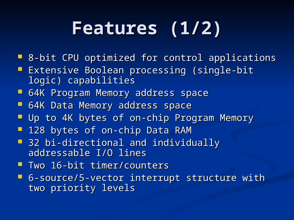
Features (1/2)Features (1/2) 8-bit CPU optimized for control applications8-bit CPU optimized for control applications Extensive Boolean processing (single-bit logic) Extensive Boolean processing (single-bit logic)
capabilitiescapabilities 64K Program Memory address space64K Program Memory address space 64K Data Memory address space64K Data Memory address space Up to 4K bytes of on-chip Program MemoryUp to 4K bytes of on-chip Program Memory 128 bytes of on-chip Data RAM128 bytes of on-chip Data RAM 32 bi-directional and individually addressable I/O 32 bi-directional and individually addressable I/O
lineslines Two 16-bit timer/countersTwo 16-bit timer/counters 6-source/5-vector interrupt structure with two 6-source/5-vector interrupt structure with two
priority levelspriority levels
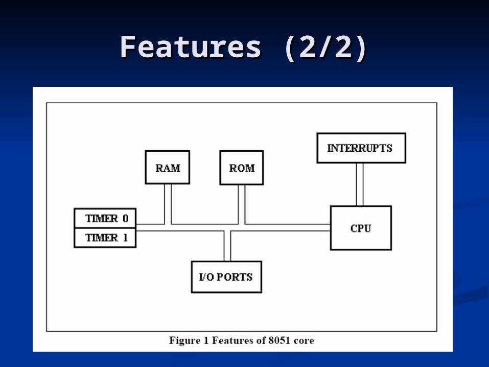
Features (2/2)Features (2/2)
OutlinesOutlines
IntroductionIntroduction ArchitectureArchitecture OperationOperation RegistersRegisters
Architecture Architecture
Memory OrganizationMemory Organization CPU ClockCPU Clock Interrupt StructureInterrupt Structure Port StructuresPort Structures Timer/CountersTimer/Counters ResetReset
Memory Organization Memory Organization (1/3)(1/3)
Logical separation of program and data Logical separation of program and data memorymemory Separate address spaces for Program (ROM) and Separate address spaces for Program (ROM) and
Data (RAM) MemoryData (RAM) Memory Allow Data Memory to be accessed by 8-bit Allow Data Memory to be accessed by 8-bit
addresses quickly and manipulated by 8-bit CPUaddresses quickly and manipulated by 8-bit CPU Program MemoryProgram Memory
Only be read, not written toOnly be read, not written to The address space is 16-bit, so maximum of 64K The address space is 16-bit, so maximum of 64K
bytesbytes Up to 4K bytes can be on-chip (internal) of 8051 coreUp to 4K bytes can be on-chip (internal) of 8051 core PSEN (Program Store Enable) is used for access to PSEN (Program Store Enable) is used for access to
external Program Memoryexternal Program Memory
Memory Organization (2/3)Memory Organization (2/3) Data MemoryData Memory
Includes 128 bytes of on-chip Data Memory whIncludes 128 bytes of on-chip Data Memory which are more easily accessible directly by its inich are more easily accessible directly by its instructions structions
There is also a number of Special Function ReThere is also a number of Special Function Registers (SFRs)gisters (SFRs)
Internal Data Memory contains four banks of Internal Data Memory contains four banks of eight registers and a special 32-byte long segmeight registers and a special 32-byte long segment which is bit addressable by 8051 bit-instrucent which is bit addressable by 8051 bit-instructionstions
External memory of maximum 64K bytes is acExternal memory of maximum 64K bytes is accessible by “movx”cessible by “movx”
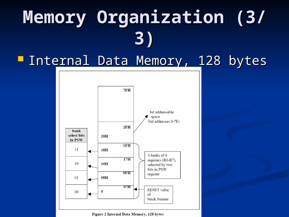
Memory Organization (3/3)Memory Organization (3/3) Internal Data Memory, 128 bytesInternal Data Memory, 128 bytes
CPU ClockCPU Clock
8051 microcontroller has a clock 8051 microcontroller has a clock input pininput pin
Interrupt StructureInterrupt Structure
The 8051 provides 4 interrupt The 8051 provides 4 interrupt sourcessources Two external interruptsTwo external interrupts Two timer interruptsTwo timer interrupts
Additional description follows in Additional description follows in Operations chapterOperations chapter
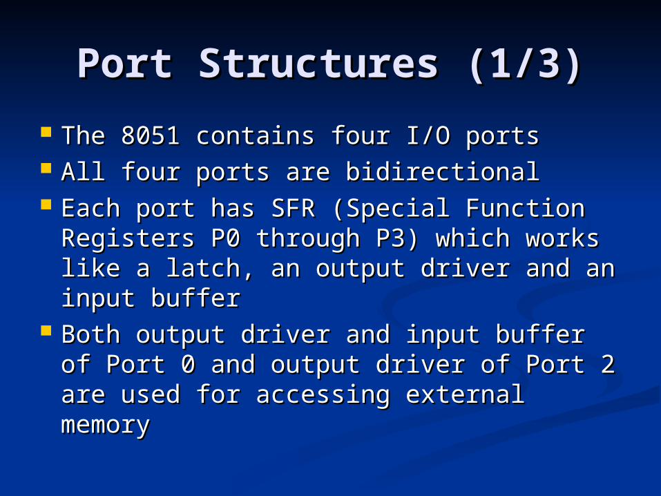
Port Structures (1/3)Port Structures (1/3)
The 8051 contains four I/O portsThe 8051 contains four I/O ports All four ports are bidirectionalAll four ports are bidirectional Each port has SFR (Special Function Each port has SFR (Special Function
Registers P0 through P3) which works Registers P0 through P3) which works like a latch, an output driver and an like a latch, an output driver and an input bufferinput buffer
Both output driver and input buffer of Both output driver and input buffer of Port 0 and output driver of Port 2 are Port 0 and output driver of Port 2 are used for accessing external memoryused for accessing external memory
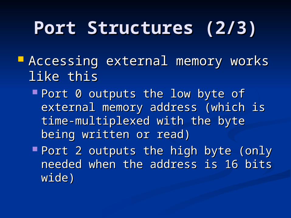
Port Structures (2/3)Port Structures (2/3) Accessing external memory works Accessing external memory works
like thislike this Port 0 outputs the low byte of external Port 0 outputs the low byte of external
memory address (which is time-memory address (which is time-multiplexed with the byte being written multiplexed with the byte being written or read)or read)
Port 2 outputs the high byte (only Port 2 outputs the high byte (only needed when the address is 16 bits needed when the address is 16 bits wide)wide)
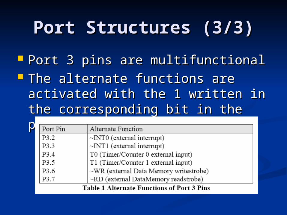
Port Structures (3/3)Port Structures (3/3) Port 3 pins are multifunctionalPort 3 pins are multifunctional The alternate functions are activated The alternate functions are activated
with the 1 written in the with the 1 written in the corresponding bit in the port SFRcorresponding bit in the port SFR
Read-Modify-Write Read-Modify-Write Feature (1/2)Feature (1/2)
When reading a port some When reading a port some instructions read the latch and instructions read the latch and others read the pinothers read the pin
The instructions that read the latch The instructions that read the latch rather than the pin are the ones that rather than the pin are the ones that read a value (possibly change it), an read a value (possibly change it), an then rewrite it to the latch are called then rewrite it to the latch are called “read-modify-write” instructions“read-modify-write” instructions
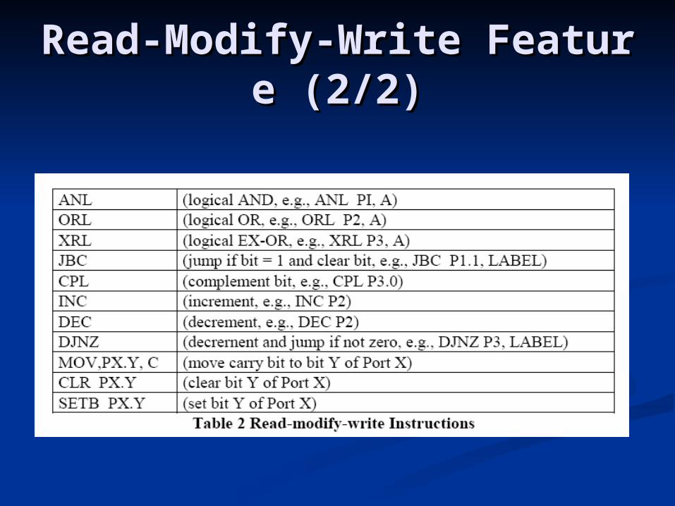
Read-Modify-Write Feature Read-Modify-Write Feature (2/2)(2/2)
Timer/CountersTimer/Counters
The 8051 has two 16-bit The 8051 has two 16-bit Timer/Counter registersTimer/Counter registers Timer 0 Timer 0 Timer 1Timer 1
Both can work either as timers or Both can work either as timers or event countersevent counters
Both have four different operating Both have four different operating modes from which to select (all modes modes from which to select (all modes are described in Operations chapter)are described in Operations chapter)
ResetReset
The reset input is the RST pinThe reset input is the RST pin
OutlinesOutlines
IntroductionIntroduction ArchitectureArchitecture OperationOperation RegistersRegisters
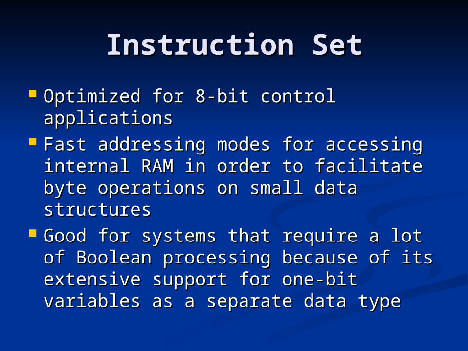
Instruction SetInstruction Set
Optimized for 8-bit control applicationsOptimized for 8-bit control applications Fast addressing modes for accessing Fast addressing modes for accessing
internal RAM in order to facilitate byte internal RAM in order to facilitate byte operations on small data structuresoperations on small data structures
Good for systems that require a lot of Good for systems that require a lot of Boolean processing because of its Boolean processing because of its extensive support for one-bit variables extensive support for one-bit variables as a separate data typeas a separate data type
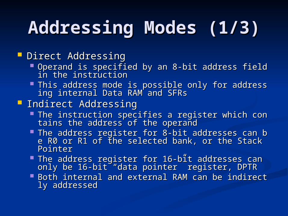
Addressing Modes (1/3)Addressing Modes (1/3) Direct AddressingDirect Addressing
Operand is specified by an 8-bit address field in the Operand is specified by an 8-bit address field in the instructioninstruction
This address mode is possible only for addressing iThis address mode is possible only for addressing internal Data RAM and SFRsnternal Data RAM and SFRs
Indirect AddressingIndirect Addressing The instruction specifies a register which contains The instruction specifies a register which contains
the address of the operandthe address of the operand The address register for 8-bit addresses can be R0 oThe address register for 8-bit addresses can be R0 o
r R1 of the selected bank, or the Stack Pointerr R1 of the selected bank, or the Stack Pointer The address register for 16-bit addresses can only bThe address register for 16-bit addresses can only b
e 16-bit “data pointer” register, DPTRe 16-bit “data pointer” register, DPTR Both internal and external RAM can be indirectly aBoth internal and external RAM can be indirectly a
ddressedddressed
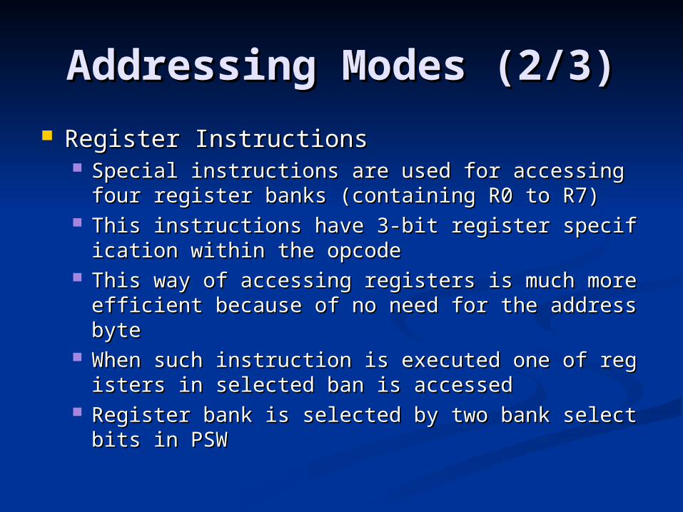
Addressing Modes (2/3)Addressing Modes (2/3) Register InstructionsRegister Instructions
Special instructions are used for accessing four rSpecial instructions are used for accessing four register banks (containing R0 to R7)egister banks (containing R0 to R7)
This instructions have 3-bit register specification This instructions have 3-bit register specification within the opcodewithin the opcode
This way of accessing registers is much more effiThis way of accessing registers is much more efficient because of no need for the address bytecient because of no need for the address byte
When such instruction is executed one of registeWhen such instruction is executed one of registers in selected ban is accessedrs in selected ban is accessed
Register bank is selected by two bank select bits iRegister bank is selected by two bank select bits in PSWn PSW
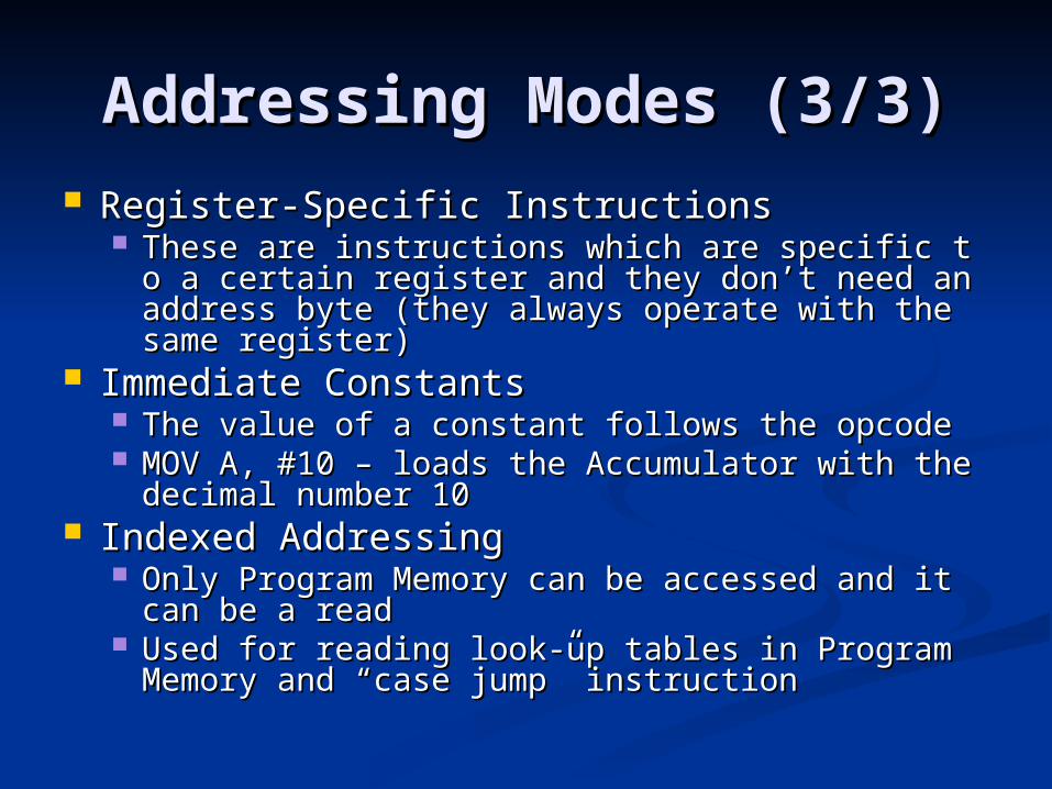
Addressing Modes (3/3)Addressing Modes (3/3) Register-Specific InstructionsRegister-Specific Instructions
These are instructions which are specific to a cerThese are instructions which are specific to a certain register and they don’t need an address byttain register and they don’t need an address byte (they always operate with the same register)e (they always operate with the same register)
Immediate ConstantsImmediate Constants The value of a constant follows the opcodeThe value of a constant follows the opcode MOV A, #10 – loads the Accumulator with the decMOV A, #10 – loads the Accumulator with the dec
imal number 10imal number 10 Indexed AddressingIndexed Addressing
Only Program Memory can be accessed and it caOnly Program Memory can be accessed and it can be a readn be a read
Used for reading look-up tables in Program MemUsed for reading look-up tables in Program Memory and “case jump” instructionory and “case jump” instruction
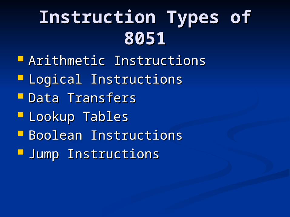
Instruction Types of Instruction Types of 80518051
Arithmetic InstructionsArithmetic Instructions Logical InstructionsLogical Instructions Data TransfersData Transfers Lookup TablesLookup Tables Boolean InstructionsBoolean Instructions Jump InstructionsJump Instructions
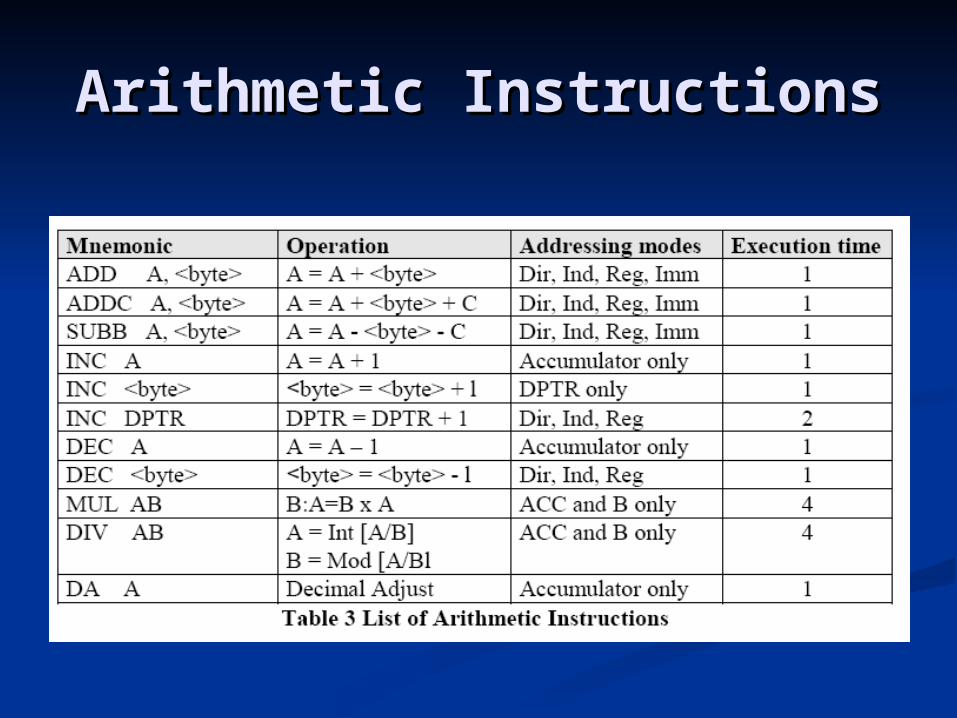
Arithmetic InstructionsArithmetic Instructions
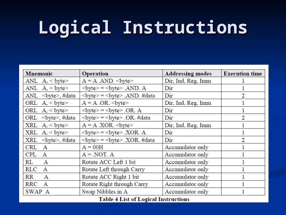
Logical InstructionsLogical Instructions
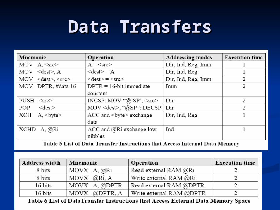
Data TransfersData Transfers
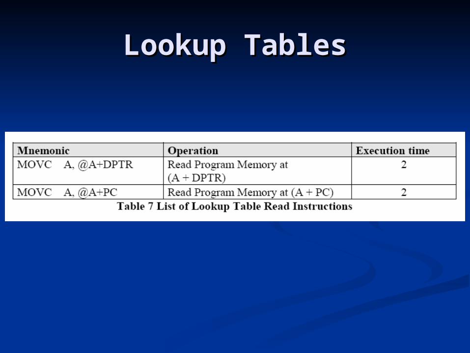
Lookup TablesLookup Tables
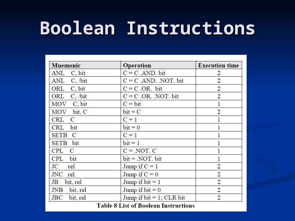
Boolean InstructionsBoolean Instructions
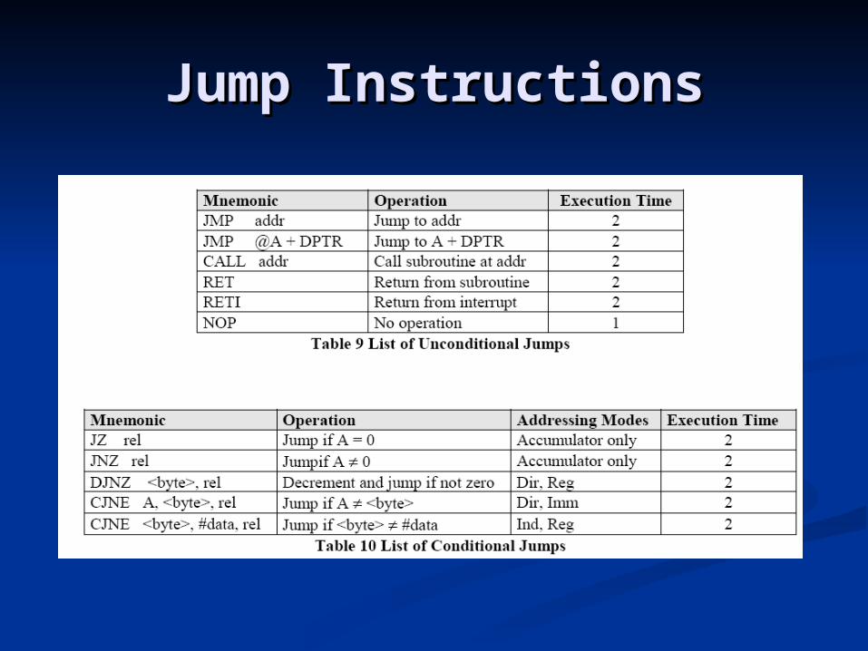
Jump InstructionsJump Instructions
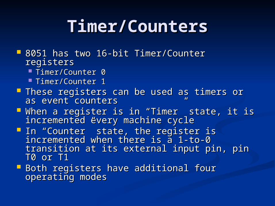
Timer/CountersTimer/Counters 8051 has two 16-bit Timer/Counter registers8051 has two 16-bit Timer/Counter registers
Timer/Counter 0Timer/Counter 0 Timer/Counter 1Timer/Counter 1
These registers can be used as timers or as These registers can be used as timers or as event countersevent counters
When a register is in “Timer” state, it is When a register is in “Timer” state, it is incremented every machine cycleincremented every machine cycle
In “Counter” state, the register is In “Counter” state, the register is incremented when there is a 1-to-0 incremented when there is a 1-to-0 transition at its external input pin, pin T0 or transition at its external input pin, pin T0 or T1T1
Both registers have additional four operating Both registers have additional four operating modesmodes
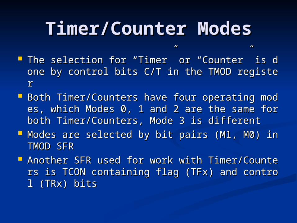
Timer/Counter ModesTimer/Counter Modes
The selection for “Timer” or “Counter” is The selection for “Timer” or “Counter” is done by control bits C/T in the TMOD registerdone by control bits C/T in the TMOD register
Both Timer/Counters have four operating moBoth Timer/Counters have four operating modes, which Modes 0, 1 and 2 are the same for des, which Modes 0, 1 and 2 are the same for both Timer/Counters, Mode 3 is differentboth Timer/Counters, Mode 3 is different
Modes are selected by bit pairs (M1, M0) in TModes are selected by bit pairs (M1, M0) in TMOD SFRMOD SFR
Another SFR used for work with Timer/CountAnother SFR used for work with Timer/Counters is TCON containing flag (TFx) and control ers is TCON containing flag (TFx) and control (TRx) bits(TRx) bits
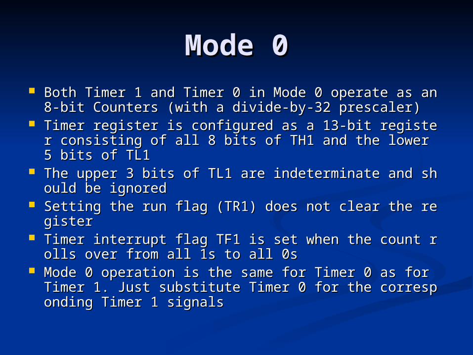
Mode 0Mode 0 Both Timer 1 and Timer 0 in Mode 0 operate as an Both Timer 1 and Timer 0 in Mode 0 operate as an
8-bit Counters (with a divide-by-32 prescaler)8-bit Counters (with a divide-by-32 prescaler) Timer register is configured as a 13-bit register consTimer register is configured as a 13-bit register cons
isting of all 8 bits of TH1 and the lower 5 bits of TL1isting of all 8 bits of TH1 and the lower 5 bits of TL1 The upper 3 bits of TL1 are indeterminate and shoulThe upper 3 bits of TL1 are indeterminate and shoul
d be ignoredd be ignored Setting the run flag (TR1) does not clear the registerSetting the run flag (TR1) does not clear the register Timer interrupt flag TF1 is set when the count rolls Timer interrupt flag TF1 is set when the count rolls
over from all 1s to all 0sover from all 1s to all 0s Mode 0 operation is the same for Timer 0 as for TimMode 0 operation is the same for Timer 0 as for Tim
er 1. Just substitute Timer 0 for the corresponding Ter 1. Just substitute Timer 0 for the corresponding Timer 1 signals imer 1 signals
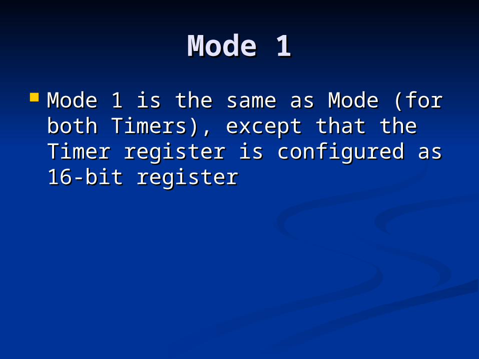
Mode 1Mode 1
Mode 1 is the same as Mode (for Mode 1 is the same as Mode (for both Timers), except that the Timer both Timers), except that the Timer register is configured as 16-bit register is configured as 16-bit registerregister
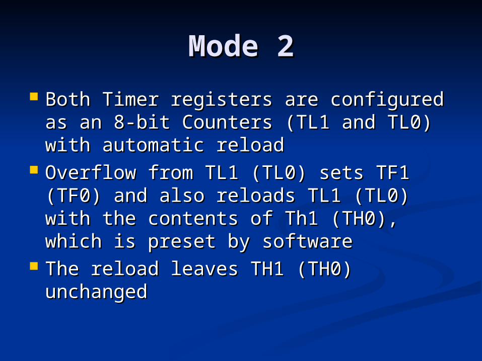
Mode 2Mode 2
Both Timer registers are configured Both Timer registers are configured as an 8-bit Counters (TL1 and TL0) as an 8-bit Counters (TL1 and TL0) with automatic reloadwith automatic reload
Overflow from TL1 (TL0) sets TF1 Overflow from TL1 (TL0) sets TF1 (TF0) and also reloads TL1 (TL0) (TF0) and also reloads TL1 (TL0) with the contents of Th1 (TH0), with the contents of Th1 (TH0), which is preset by softwarewhich is preset by software
The reload leaves TH1 (TH0) The reload leaves TH1 (TH0) unchangedunchanged
Mode 3Mode 3 Mode 3 is different for Timer 1 and Timer 0Mode 3 is different for Timer 1 and Timer 0 Timer 1 just holds its count. It operates the same as Timer 1 just holds its count. It operates the same as
when TR1 is set to 0when TR1 is set to 0 For Timer 0 is different, TL0 and TH0 of Timer 0 are For Timer 0 is different, TL0 and TH0 of Timer 0 are
established as two separate countersestablished as two separate counters TL0 uses Timer 0 control bits for its work: C/T, TL0 uses Timer 0 control bits for its work: C/T,
GATE, TR0, ~INT0, and TF0GATE, TR0, ~INT0, and TF0 TH0 is locked into a timer function (counting TH0 is locked into a timer function (counting
machine cycles) and takes over the use of TR1 and machine cycles) and takes over the use of TR1 and TF1 from Timer 1. TH0 is now actually in control of TF1 from Timer 1. TH0 is now actually in control of “Timer 1” interrupt“Timer 1” interrupt
Mode 3 is provided for applications that require an Mode 3 is provided for applications that require an extra 8-bit timer or counterextra 8-bit timer or counter With Timer 0, 8051 looks like it has three Timer/CountersWith Timer 0, 8051 looks like it has three Timer/Counters When Timer 0 in Mode 3, Timer 1 can be turned on and off When Timer 0 in Mode 3, Timer 1 can be turned on and off
by switching it out of and into its own Mode 3, or can still by switching it out of and into its own Mode 3, or can still be used in any application not requiring an interruptbe used in any application not requiring an interrupt
Interrupt (1/3)Interrupt (1/3)
8051 provides 4 interrupt sources8051 provides 4 interrupt sources 2 external interrupts2 external interrupts 2 timer interrupts2 timer interrupts
They are controlled via two SFRs, IE and They are controlled via two SFRs, IE and IPIP
Each interrupt source can be individuallEach interrupt source can be individually enabled or disabled by setting or cleariy enabled or disabled by setting or clearing a bit in IE (Interrupt Enable). IE also eng a bit in IE (Interrupt Enable). IE also exists a global disable bit, which can be clxists a global disable bit, which can be cleared to disable all interrupts at onceeared to disable all interrupts at once
Interrupt (2/3)Interrupt (2/3) Each interrupt source can also be individually Each interrupt source can also be individually
set to one of two priority levels by setting or set to one of two priority levels by setting or clearing a bit in IP (Interrupt Priority)clearing a bit in IP (Interrupt Priority)
A low-priority interrupt can be interrupted by A low-priority interrupt can be interrupted by high-priority interrupt, but not by another high-priority interrupt, but not by another low-priority onelow-priority one
A high-priority interrupt can’t be interrupted A high-priority interrupt can’t be interrupted by any other interrupt sourceby any other interrupt source
If interrupt requests of the same priority level If interrupt requests of the same priority level are received simultaneously, an internal are received simultaneously, an internal polling sequence determines which request is polling sequence determines which request is serviced, so within each priority lever there is serviced, so within each priority lever there is a second priority structurea second priority structure
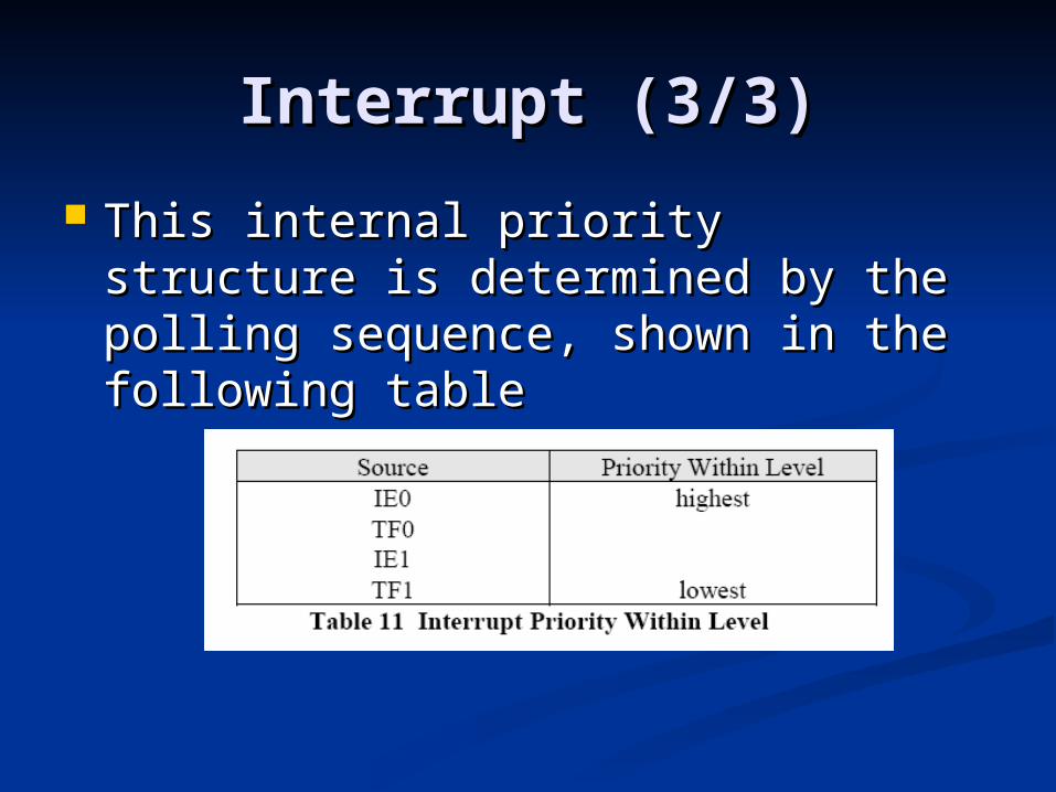
Interrupt (3/3)Interrupt (3/3) This internal priority structure is This internal priority structure is
determined by the polling sequence, determined by the polling sequence, shown in the following tableshown in the following table
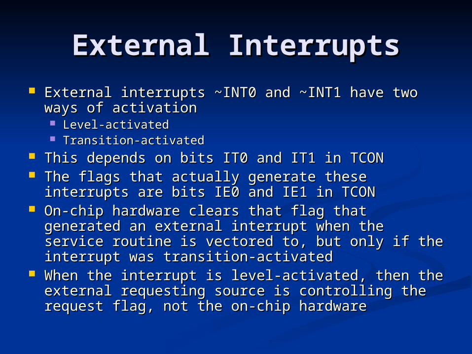
External InterruptsExternal Interrupts External interrupts ~INT0 and ~INT1 have two External interrupts ~INT0 and ~INT1 have two
ways of activationways of activation Level-activatedLevel-activated Transition-activatedTransition-activated
This depends on bits IT0 and IT1 in TCONThis depends on bits IT0 and IT1 in TCON The flags that actually generate these interrupts are The flags that actually generate these interrupts are
bits IE0 and IE1 in TCONbits IE0 and IE1 in TCON On-chip hardware clears that flag that generated an On-chip hardware clears that flag that generated an
external interrupt when the service routine is external interrupt when the service routine is vectored to, but only if the interrupt was transition-vectored to, but only if the interrupt was transition-activatedactivated
When the interrupt is level-activated, then the When the interrupt is level-activated, then the external requesting source is controlling the request external requesting source is controlling the request flag, not the on-chip hardwareflag, not the on-chip hardware
Timer 0 and Timer 1 Timer 0 and Timer 1 InterruptsInterrupts
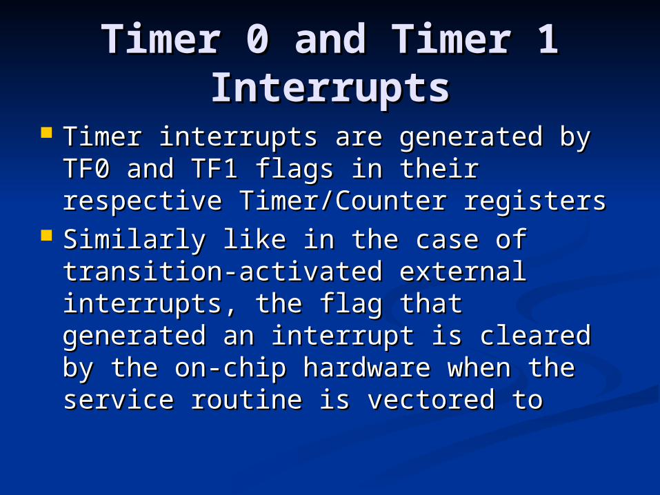
Timer interrupts are generated by Timer interrupts are generated by TF0 and TF1 flags in their respective TF0 and TF1 flags in their respective Timer/Counter registersTimer/Counter registers
Similarly like in the case of Similarly like in the case of transition-activated external transition-activated external interrupts, the flag that generated interrupts, the flag that generated an interrupt is cleared by the on-an interrupt is cleared by the on-chip hardware when the service chip hardware when the service routine is vectored toroutine is vectored to
Handling of Interrupts Handling of Interrupts (1/5)(1/5)
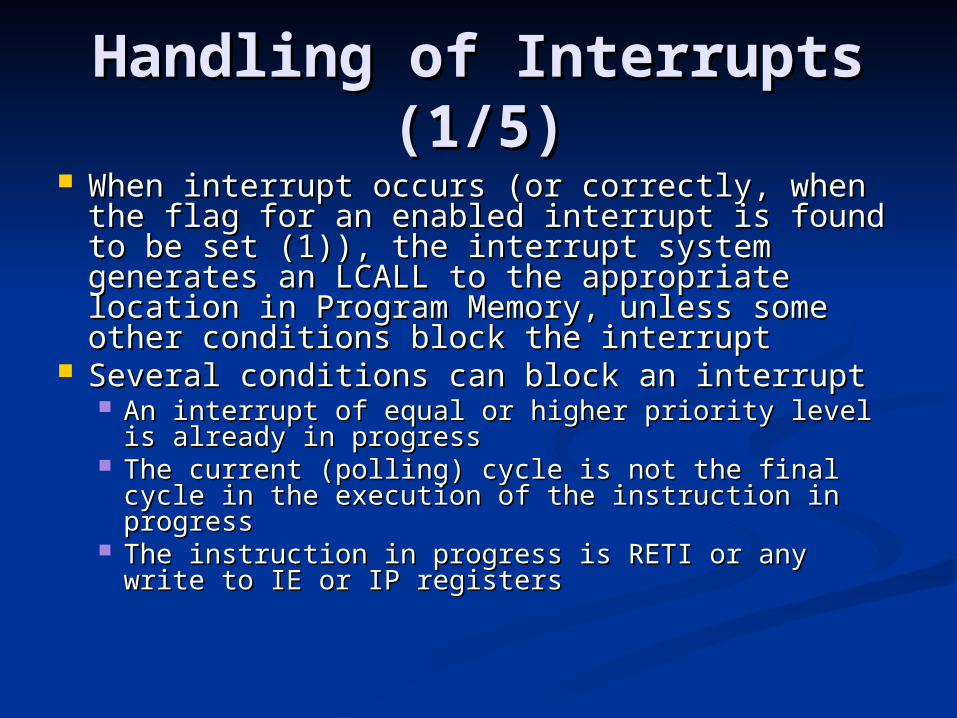
When interrupt occurs (or correctly, when When interrupt occurs (or correctly, when the flag for an enabled interrupt is found the flag for an enabled interrupt is found to be set (1)), the interrupt system to be set (1)), the interrupt system generates an LCALL to the appropriate generates an LCALL to the appropriate location in Program Memory, unless some location in Program Memory, unless some other conditions block the interruptother conditions block the interrupt
Several conditions can block an interruptSeveral conditions can block an interrupt An interrupt of equal or higher priority level is An interrupt of equal or higher priority level is
already in progressalready in progress The current (polling) cycle is not the final cycle The current (polling) cycle is not the final cycle
in the execution of the instruction in progressin the execution of the instruction in progress The instruction in progress is RETI or any The instruction in progress is RETI or any
write to IE or IP registerswrite to IE or IP registers
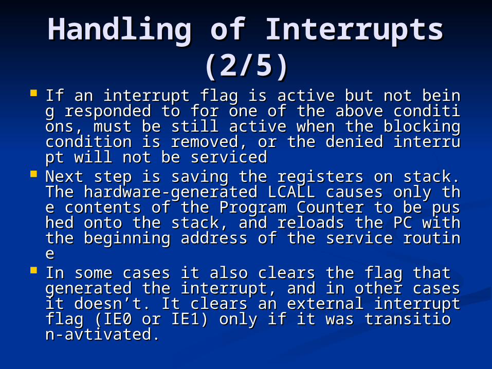
Handling of Interrupts (2/5)Handling of Interrupts (2/5) If an interrupt flag is active but not being resIf an interrupt flag is active but not being res
ponded to for one of the above conditions, ponded to for one of the above conditions, must be still active when the blocking conditmust be still active when the blocking condition is removed, or the denied interrupt will ion is removed, or the denied interrupt will not be servicednot be serviced
Next step is saving the registers on stack. ThNext step is saving the registers on stack. The hardware-generated LCALL causes only the hardware-generated LCALL causes only the contents of the Program Counter to be puse contents of the Program Counter to be pushed onto the stack, and reloads the PC with thed onto the stack, and reloads the PC with the beginning address of the service routinehe beginning address of the service routine
In some cases it also clears the flag that geneIn some cases it also clears the flag that generated the interrupt, and in other cases it doerated the interrupt, and in other cases it doesn’t. It clears an external interrupt flag (IE0 sn’t. It clears an external interrupt flag (IE0 or IE1) only if it was transition-avtivated.or IE1) only if it was transition-avtivated.
Handling of Interrupts (3/5)Handling of Interrupts (3/5) Having only PC be automatically saved gives Having only PC be automatically saved gives
programmer more freedom to decide how programmer more freedom to decide how much time to spend saving other registers. much time to spend saving other registers. Programmer must also be more careful with Programmer must also be more careful with proper selection, which register to saveproper selection, which register to save
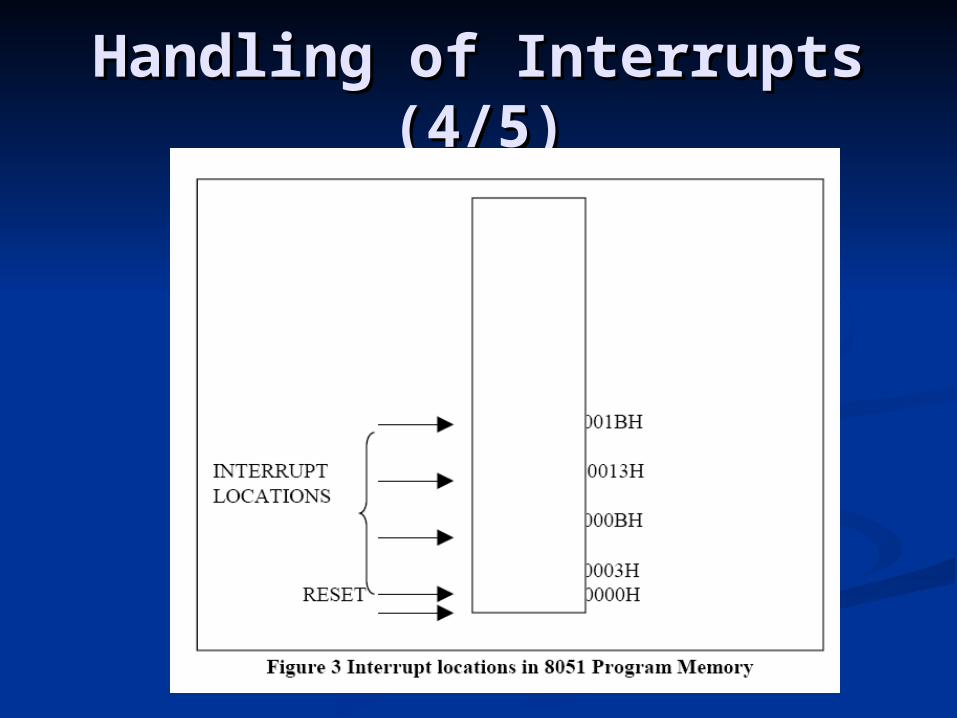
The service routine for each interrupt begins The service routine for each interrupt begins at a fixed location. The interrupt locations are at a fixed location. The interrupt locations are spaced at 8-byte interval, beginning at 0003H spaced at 8-byte interval, beginning at 0003H for External Interrupt 0, 000BH for Timer 0, for External Interrupt 0, 000BH for Timer 0, 0013H for External Interrupt 1 and 001BH 0013H for External Interrupt 1 and 001BH for Timer 1, shown in the following tablesfor Timer 1, shown in the following tables
Handling of Interrupts (4/5)Handling of Interrupts (4/5)
Handling of Interrupts (5/5)Handling of Interrupts (5/5) Execution of service routine continues from Execution of service routine continues from
that location until the end, that is until it that location until the end, that is until it encounters RETI.encounters RETI.
RETI instruction does two thingsRETI instruction does two things It informs the processor that this interrupt routine is It informs the processor that this interrupt routine is
finishedfinished Secondly, reloads the PC from the top bytes from the Secondly, reloads the PC from the top bytes from the
stackstack Similar result could be accomplished with RET, Similar result could be accomplished with RET,
with the distinction that the interrupt control with the distinction that the interrupt control system would be thinking an interrupt was still system would be thinking an interrupt was still in progressin progress
ResetReset The reset input is RST pinThe reset input is RST pin To accomplish a reset the RST pin must be held high for To accomplish a reset the RST pin must be held high for
at least two machine cyclesat least two machine cycles In the response on the RST signal, CPU generates an inteIn the response on the RST signal, CPU generates an inte
rnal resetrnal reset The external reset signal is asynchronous to the internal The external reset signal is asynchronous to the internal
clockclock In the internal reset algorithm, 0s are written to all the SIn the internal reset algorithm, 0s are written to all the S
FRs except the port latches and Stack PointerFRs except the port latches and Stack Pointer The port latches are initialized to FFH and Stack Pointer The port latches are initialized to FFH and Stack Pointer
to 07Hto 07H Driving ALE and PSEN pins to 0 while reset is active coulDriving ALE and PSEN pins to 0 while reset is active coul
d cause the device to go into an indeterminate stated cause the device to go into an indeterminate state The internal RAM is not affected by reset. On power up tThe internal RAM is not affected by reset. On power up t
he RAM content is indeterminatehe RAM content is indeterminate
OutlinesOutlines
IntroductionIntroduction ArchitectureArchitecture OperationOperation RegistersRegisters
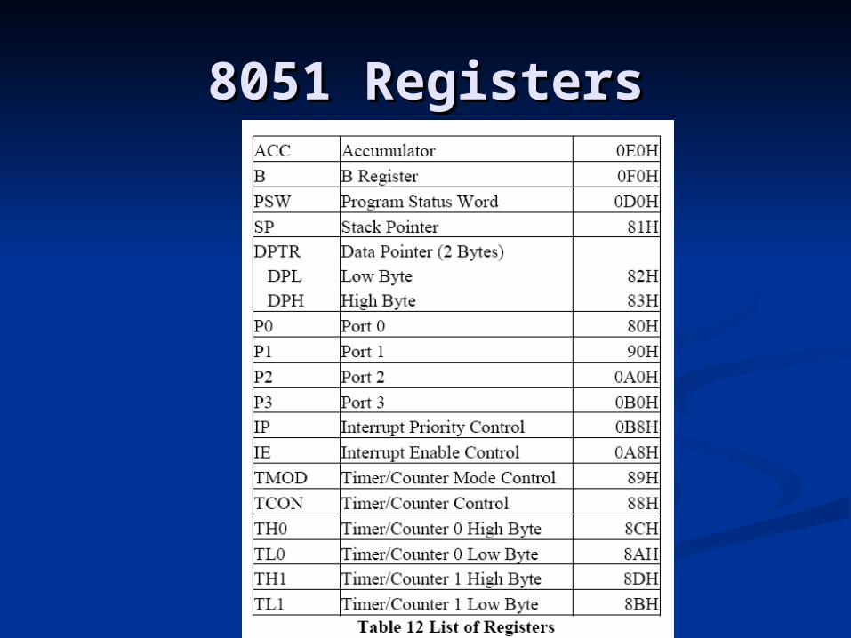
8051 Registers8051 Registers
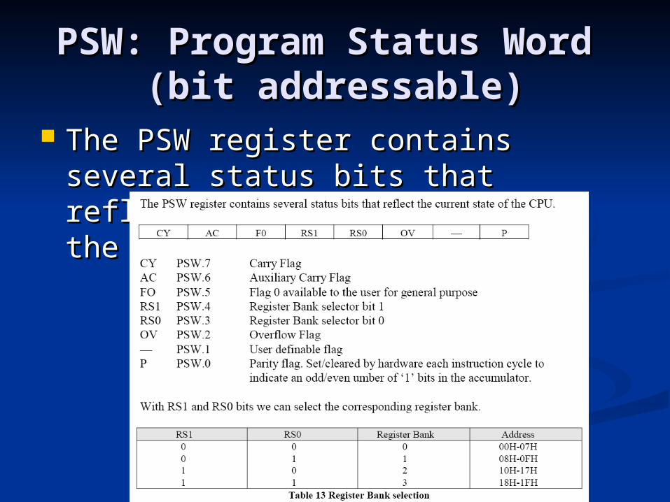
PSW: Program Status Word PSW: Program Status Word (bit addressable)(bit addressable)
The PSW register contains several The PSW register contains several status bits that reflect the current status bits that reflect the current state of the CPUstate of the CPU
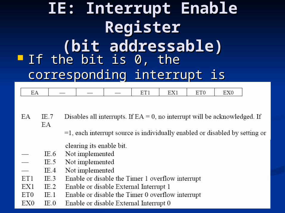
IE: Interrupt Enable IE: Interrupt Enable RegisterRegister
(bit addressable)(bit addressable) If the bit is 0, the corresponding If the bit is 0, the corresponding
interrupt is disabled. Otherwise, the interrupt is disabled. Otherwise, the interrupt is enabled.interrupt is enabled.
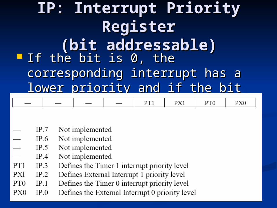
IP: Interrupt Priority IP: Interrupt Priority RegisterRegister
(bit addressable)(bit addressable) If the bit is 0, the corresponding If the bit is 0, the corresponding
interrupt has a lower priority and if interrupt has a lower priority and if the bit is 1, the interrupt has a the bit is 1, the interrupt has a higher priorityhigher priority
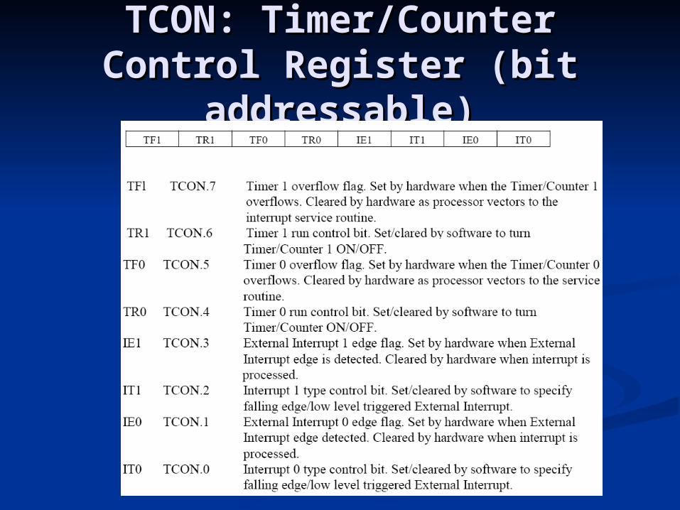
TCON: Timer/Counter TCON: Timer/Counter Control Register (bit Control Register (bit
addressable)addressable)
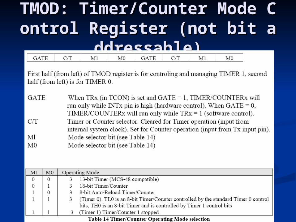
TMOD: Timer/Counter Mode CTMOD: Timer/Counter Mode Control Register (not bit addressontrol Register (not bit address
able)able)