8085 tengu - 8085 projects€¦ · summary...
TRANSCRIPT

8085 TENGU
EC-316 MICROPROCESSORS LABELECTRONICS AND COMMUNICATION DEPARTMENT
NETAJI SUBHAS INSTITUTE OF TECHNOLOGYDELHI UNIVERSITY
DHRUV KHARE 53/EC/13&
ISHA CHAUDHRY 65/EC/132ND JUNE 2016

SUMMARY8085 Tengu is a toy which responds to sound waves and sings along with them. It isbased on the 8085 microprocessor. The sound is sent as an input via an audioamplifier which amplifies the waves. The amplified waves are then passed through aclipping diode to generate a square wave. This square wave is forwarded to 8254which is a Programmable Interval Timer and counts the frequency of the inputwave.This frequency value is processed by 8085 and depending on the frequency aface is depicted on the LED matrix. This is device is quite an attraction for children.
JUSTIFICATIONWe had planned to make a very different project but Prof. D.V. Gadre encouraged usto make 8085 Tengu. At first we were daunted by the challenge since it is a projectalready made both by our seniors and sir himself. However, after thorough study werealized it would be an interesting project to work on and hence continued to work onit.
This project has taught us the value of electronics and how small independent partscan be brought together to create something special.
This experience has been wonderful and we have learnt how to be patient and howto work together without getting on each others nerves. We have also learnt theimportance of time management and self belief.

ACKNOWLEDGEMENTWe are extremely grateful to Prof. D.V. Gadre for encouraging us throughoutthe entire process of making this project. Without his guidance we wouldn’thave been able to accomplish this project. We are also grateful toMrs.Sangeeta Gadre for giving us more ideas and Mr. Akash Gupta for hisconstant guidance and help. A very special thanks to our parents and ourfriends especially Gaurav Tyagi, Arun Kumar, Anshuman Mishra, Gaurav Kumar,Anirudh Rustagi, and Ishaan Kubba for helping us throughout.

TABLE OF CONTENTS
S NO. TOPIC
1 SUMMARY
2 JUSTIFICATION
3 ACKNOWLEDGEMENT
4. MATERIAL REQUIRED
5. A LOOK INTO THE SCHEMATIC
6. A LOOK INTO SCHEMATIC OF THE LED MATRIX
7. MAIN BLOCK DIAGRAM
8. THE AUDIO AMPLIFIER
9. THE 8254
10. THE 8085
11. LED MATRIX
12. RAM AND ROM
13. DECODING CIRCUIT
14. THE TRANSISTOR ARRAYS
15. THE LATCHES
16. PROJECT FILES
17. THE CODE
18. TESTING THE BOARD
19. PROBLEMS FACED
20. CONCLUSION
21. BIBLIOGRAPHY

MATERIAL REQUIRED
S NO. NAME OF COMPONENT
1. RESISTORS
2. CAPACITORS
3. 8085
4. 8253/54
5. LATCHES- 74573N
6. DECODER-74138N
7. TRANSISTOR ARRAY (UDN2981A &ULN2803A)
8. 8K EEPROM
9. 8K RAM
10. GREEN LEDS AND RED LEDS
11. SMD MICRO USB PORT
12. EEPROM PROGRAMMER
13. SLIDE SWITCH
14. PUSHBUTTONs
15. BERG STRIP
16. NAND GATE 7400
17. NOT GATE 7404

LOOK INTO THE SCHEMATIC

A LOOK INTO THE SCHEMATICOF THE LED MATRIX

THE AUDIO AMPLIFIER

THE 8254
The 8254 is a programmable interval timer. It has 3 16-bit (down) countersthat can operate independently in any of the 6 modes. In our project wehave used all three for different purposes.
The first counter, COUNTER 0 is used to read the frequency of the audioinput being received from the audio amplifier. The output of the audioamplifier acts like a clock to COUNTER 0. COUNTER 0 operating in mode1 counts down from 4E20 (equivalent to 20,000 in decimal) at thenegative edge of the square wave audio input. The value in this counteris latched continuously and is read after every 1 second and we get theaverage frequency of the input audio waves in that 1 second. We usethis value to display various faces.
The second and third counter ie. COUNTER 1 and COUNTER 2 operate inmode 2. These 2 counters are used together to generate the 1 secondinterrupt to pin RST 7.5 of 8085 and to reset the count of COUNTER 0 to20,000. The 1 second interrupt is generated to request 8085 to read thelatched value of COUNTER 0. The counter latch command is used in themain program to continuously latch the value, and this value is saved inthe RAM for future use during ISR.
Since only A7 is being used to select the chip, and A1 and A0 are beingused to select the 3 counters and control word register of 8254therefore we have the addresses as:
COUNTER 0 80H
COUNTER 1 81H
COUNTER 2 82H
CONTROL WORD REGISTER 83H

THE 8085
The brain of our circuit- microprocessor 8085. The condensor mic provides the input.The audio amplification circuit amplifies the input audio waves, and a zener diode isused to clip these waves to form square waves. The 8254 counts the frequency of thissquare wave and also helps in interrupting 8085.
The 8085 on receiving the interrupt jumps to the ISR to service the request. Here it readsthe latched value of COUNTER 0 from the RAM. After making comparisons anddetermining the range in which the input frequency lies it displays different faces on theLED MATRIX.
In the main program the 8085 multiplexes the desired values to display a face. In theprocess of multiplexing we first send the column values (in-order to select a particularcolumn) and then we send the values to light up multiple LEDs in that column.
Eg: Suppose we have to light the THE 2ND LED of the 1ST row on the board the codewould be as follows
MVI A , 10H 7 T statesSTA, A000H 13T statesMVI A , 02H 7 T statesSTA ,8000H 13T states
It is very important to note that in our matrix we have conducted column multiplexingie. We select one column and switch its LEDs ON and then move to the next column andso on. At a particular instant of time, any LED of one particular column only will light up.
Since there are 8 columns , we are actually dividing the face into 8 parts. In-order to seethe complete face we need to switch between the columns really fast to meet thepersistence of vision, ie we need to display all the columns within 1/16th of a second.Thisis very easy since the clock frequency is 2Mhz.
The time duration to execute the above 4 commands is = (7+13+7+13)*(0.5us)= 20usThe time duration to switch off the LEDs to prevent generation of Ghost LEDs= 20usTime delays= 1656us ( 1 time delay after switching the LEDs on and 1 after switchingthem off. This is done to remove ghost LEDs)Total time between two columns= 1696us or 1.6ms

THE LED MATRIX
One can easily choose whether to take up column multiplexing or row multiplexing depending onthe LED matrix design. We have done column multiplexing.
To light up one red LED we need a current of approximately 15-20mA. Since we are changing thecolumns so fast it is almost as if we are powering all the rows at the same time therefore weneed higher amount of current.
To ensure that the right amount current flows in the LEDs we use the following formula:R = ( V - VLED)/ (8*IMIN )Here V is the power supply voltage in our case 5V
VLED is the voltage drop across the LED approxiamtely 1.7VIMIN is the minimum current we need across the LEDs.
We have taken IMIN to be 4mA. Therefore R=100 ohm. The peak current at any point of timewould be 32mA.

THE RAM AND ROM
RAM or Random Access Memory is used basically to store data while running theprogram. We can both read and write data into it. In our project we have usedthe RAM majorly to store the latched values of the COUNTER 0 of 8254. Thismemory is volatile. When the power is turned off, all its contents are destroyed.
ROM or Read Only Memory is the main memory of the brain 8085. 8085 fetchesinstructions saved sequentially in the ROM. Saved on the ROM is the entireprogram that the 8085 has to execute. We can only read from the ROM once it isconnected to the board.We have used EEPROM which is Electrically ErasableProgrammable Read Only Memory, since the information stored in this memorycan be altered using electrical signals. Unlike RAM its contents do not getdestroyed when power is turned off and to write data into it we need anEEPROM programmer.
RAM and ROM come in various sizes. We have chosen 8K ROM and 8K RAM. Ourwork could have been easily accomplished by 2K ROM and 2K RAM but to be onthe safe side we took a larger memory. A larger memory leads to slightvariations only in the interfacing circuitry rest of the connections remain thesame.

THE DECODING CIRCUIT
The decoding circuit is basically used to enable the RAM,ROM and the I/O devices atthe right time.
A decoder identifies each combination at its input and decodes it into its binaryequivalent. It is commonly used in interfacing I/O peripherals and memory. Decodersare also in-built in memory chip to select specific registers in it.
In our project we have used 3x8 decoder(in-order to accommodate any future changeas well).
Address lines A15, A14 and,A13 have been used as input to decoder 74138
A15 A14 A13 LOGIC
0 0 0 ROM ENABLE
0 1 0 RAM ENABLE
1 0 0 LED ROW ENABLE
1 0 1 LED COLUMN ENABLE
The decoder circuit can be replaced by use of logic gates.

THE TRANSISTOR ARRAYS
8085 can not source or sink currents required by the LEDs hence we needdriver ICs. Therefore we make use of UDN2981A and ULN2803A driver ICs forthe LED MATRIX.
UDN2981A is an 8- channel source driver. It is an PNP transistor array.
ULN2803A is an 8-channel Darlington Array. It is used for sinking the current.

THE LATCHES
LATCH 2 and LATCH 3 are being usedto latch the data of the column androws respectively.(The notationsmay seem ambiguous but latch 2 isconnected to LEDROW to send in thecontrol word in the form of a rowarray in order to select a particularcolumn.) These are required so thatthe LED MATRIX only displays thevalues we need to display and notnot all values that are present on thebidirectional data bus.
LATCH 2 is enabled when
A15 A14 A13 - 1 0 0IO/M- is LOWWR- is LOW
LATCH 3 is enabled when
A15 A14 A13 - 1 0 1IO/M- is LOWWR- is LOW
LATCH 1 is being used to latch the values of A0-A7. The lower order address bus of 8085 uP ismultiplexed with the data bus. In executing an instruction, in earlier part of the machine cycle AD0-AD7 are used as low-order address lines. During the latter part of the cycle, these lines are used asdata bus.Hence we need the latch. This latch is enabled by ALE pin of 8085. ALE is a positive goingpulse generated every time the 8085 begins an operation.
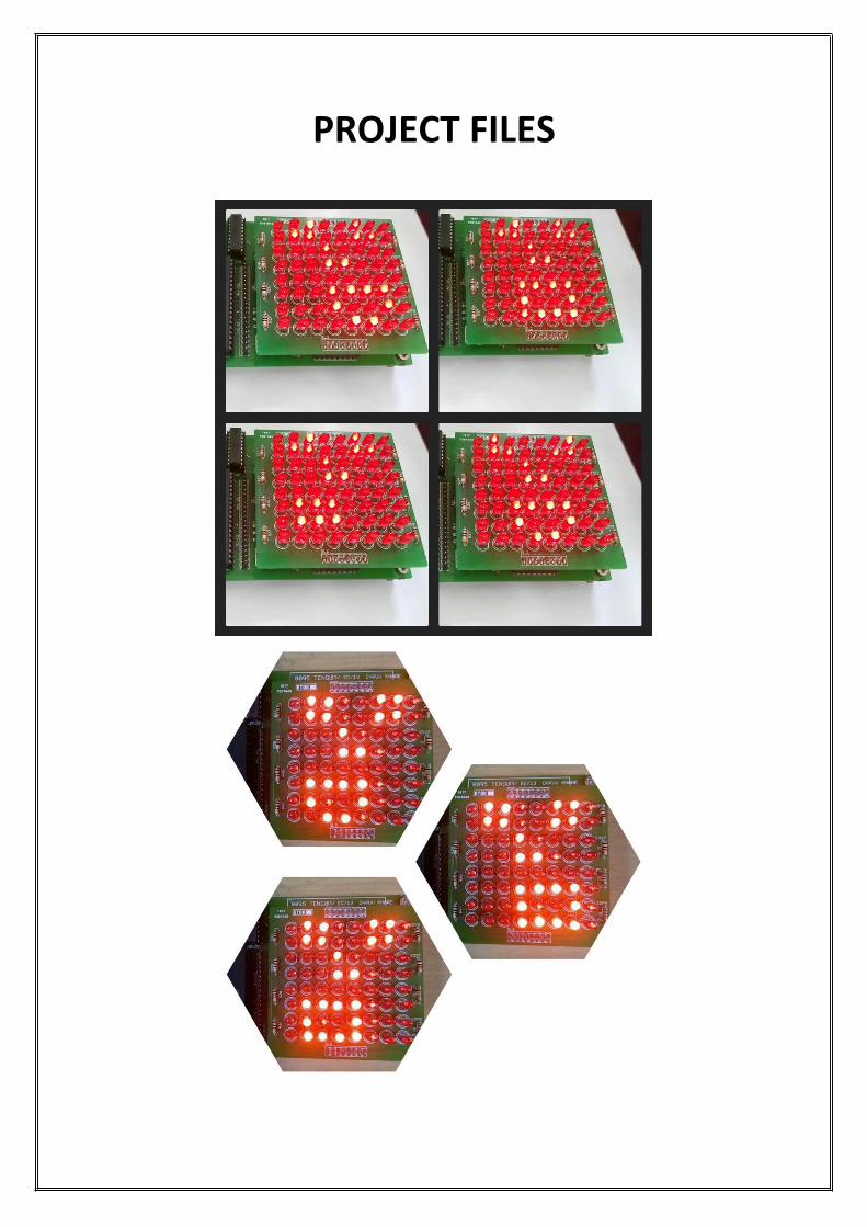
PROJECT FILES

THE CODE.ORG 0000H
JMP 0040H.ORG 003CHJMP 0500H.ORG 0040HLXI SP,05000HMVI A,00BHSIMEILXI H,01000HMOV A,HSTA 04502HMOV A,LSTA 04503HMVI A,032HOUT 083HMVI A,020HOUT 080HMVI A,04EHOUT 080HMVI A,074HOUT 083HMVI A,050HOUT 081HMVI A,0C3HOUT 081HMVI A,094HOUT 083HMVI A,028HOUT 082H
LOOP3: MVI B,008HLDA 04502HMOV H,ALDA 04503HMOV L,A
LOOP: MOV A,MSTA 08000HINX HMOV A,MSTA 0A000HINX HCALL DELAYMVI A,00HSTA 08000HMVI A,00HSTA 0A000HCALL DELAYMVI A,0D2H ;LATCHING FROM COUNTER 0OUT 083HIN 080HSTA 04500Hxra aIN 80HSTA 04501HDCR BJNZ LOOPJMP LOOP3.ORG 0500HLDA 04501H ;ISRCPI 04BH ;FACE3 CHECKJNC LOCA3CPI 04AH ;FACE4 CHECKJNC LOCA4CPI 049H ;FACE5 CHECKJNC LOCA5

CPI 048H ;FACE6 CHECKJNC LOCA6CPI 047H ;FACE7 CHECKJNC LOCA7CPI 046H ;FACE8 CHECKJNC LOCA8CPI 045H ;FACE9 CHECKJNC LOCA9CPI 044H ;FACE10 CHECKJNC LOCA10CPI 043H ;FACE11 CHECKJNC LOCA11CPI 042H ;FACE12 CHECKJNC LOCA12CPI 041H ;FACE13 CHECKJNC LOCA13CPI 040H ;FACE14 CHECKJNC LOCA14CPI 03FH ;FACE15 CHECKJNC LOCA15CPI 03EH ;FACE16 CHECKJNC LOCA1CPI 03DH ;FACE17 CHECKJNC LOCA2CPI 03CH ;FACE18 CHECKJNC LOCA3CPI 03BH ;FACE19 CHECKJNC LOCA4CPI 03AH ;FACE20 CHECKJNC LOCA5CPI 039H ;FACE21 CHECKJNC LOCA6CPI 038H ;FACE22 CHECKJNC LOCA7CPI 037H ;FACE23 CHECKJNC LOCA8CPI 036H ;FACE24 CHECKJNC LOCA9CPI 035H ;FACE25 CHECKJNC LOCA10CPI 034H ;FACE26 CHECKJNC LOCA11CPI 033H ;FACE27 CHECKJNC LOCA12CPI 032H ;FACE28 CHECKJNC LOCA13CPI 031H ;FACE29 CHECKJNC LOCA14CPI 030H ;FACE30 CHECKJNC LOCA15CPI 02FH ;FACE31 CHECKJNC LOCA1CPI 02EH ;FACE32 CHECKJNC LOCA2CPI 02DH ;FACE33 CHECKJNC LOCA3CPI 02CH ;FACE34 CHECKJNC LOCA4CPI 02BH ;FACE35 CHECKJNC LOCA5CPI 02AH ;FACE36 CHECKJNC LOCA6CPI 029H ;FACE37 CHECKJNC LOCA7CPI 028H ;FACE38 CHECKJNC LOCA8CPI 027H ;FACE39 CHECKJNC LOCA9CPI 026H ;FACE40 CHECKJNC LOCA10

CPI 025H ;FACE41 CHECKJNC LOCA11CPI 024H ;FACE42 CHECKJNC LOCA12CPI 023H ;FACE43 CHECKJNC LOCA13CPI 022H ;FACE44 CHECKJNC LOCA14CPI 021H ;FACE45 CHECKJNC LOCA15CPI 020H ;FACE46 CHECKJNC LOCA1CPI 01FH ;FACE47 CHECKJNC LOCA2CPI 01EH ;FACE48 CHECKJNC LOCA3CPI 01DH ;FACE49 CHECKJNC LOCA4CPI 01CH ;FACE50 CHECKJNC LOCA5CPI 01BH ;FACE51 CHECKJNC LOCA6CPI 01AH ;FACE52 CHECKJNC LOCA7CPI 019H ;FACE53 CHECKJNC LOCA8CPI 018H ;FACE54 CHECKJNC LOCA9CPI 017H ;FACE55 CHECKJNC LOCA10CPI 016H ;FACE56 CHECKJNC LOCA11CPI 015H ;FACE57 CHECKJNC LOCA12CPI 014H ;FACE58 CHECKJNC LOCA13CPI 013H ;FACE59 CHECKJNC LOCA14CPI 012H ;FACE60 CHECKJNC LOCA15CPI 011H ;FACE61 CHECKJNC LOCA1CPI 010H ;FACE62 CHECKJNC LOCA2CPI 00FH ;FACE63 CHECKJNC LOCA3CPI 00EH ;FACE64 CHECKJNC LOCA4CPI 00DH ;FACE65 CHECKJNC LOCA5CPI 00CH ;FACE66 CHECKJNC LOCA6CPI 00BH ;FACE67 CHECKJNC LOCA7CPI 00AH ;FACE68 CHECKJNC LOCA8CPI 009H ;FACE69 CHECKJNC LOCA9CPI 008H ;FACE70 CHECKJNC LOCA10CPI 007H ;FACE71 CHECKJNC LOCA11CPI 006H ;FACE72 CHECKJNC LOCA12CPI 005H ;FACE73 CHECKJNC LOCA13CPI 004H ;FACE74 CHECKJNC LOCA14CPI 003H ;FACE75 CHECKJNC LOCA15

MVI A,000HSTA 04503H
LOCA: EIRET
LOCA1: MVI A,00HSTA 04503HJMP LOCA
LOCA2: MVI A,010HSTA 04503HJMP LOCA
LOCA3: MVI A,020HSTA 04503HJMP LOCA
LOCA4: MVI A,030HSTA 04503HJMP LOCA
LOCA5: MVI A,040HSTA 04503HJMP LOCA
LOCA6: MVI A,050HSTA 04503HJMP LOCA
LOCA7: MVI A,060HSTA 04503HJMP LOCA
LOCA8: MVI A,070HSTA 04503HJMP LOCA
LOCA9: MVI A,080HSTA 04503HJMP LOCA
LOCA10: MVI A,090HSTA 04503HJMP LOCA
LOCA11: MVI A,0A0HSTA 04503HJMP LOCA
LOCA12: MVI A,0B0HSTA 04503HJMP LOCA
LOCA13: MVI A,0C0HSTA 04503HJMP LOCA
LOCA14: MVI A,0D0HSTA 04503HJMP LOCA
LOCA15: MVI A,0E0HSTA 04503HJMP LOCA.ORG 0750H
DELAY: LXI D,00045HLOOP2: DCX D
MOV A,EORA DJNZ LOOP2RET.ORG 1000H
LOOKUP: .db 001H,000H,002H,002H,004H,0E3H,008H,0ACH,010H,0A8H,020H,0E3H,040H,002H,080H,000H.db 001H,000H,002H,003H,004H,062H,008H,0ACH,010H,0A8H,020H,062H,040H,003H,080H,000H.db 001H,000H,002H,002H,004H,063H,008H,06CH,010H,068H,020H,063H,040H,002H,080H,000H.db 001H,000H,002H,003H,004H,002H,008H,06CH,010H,068H,020H,062H,040H,003H,080H,000H.db 001H,000H,002H,002H,004H,003H,008H,06CH,010H,0A8H,020H,0A3H,040H,062H,080H,000H.db 001H,000H,002H,003H,004H,002H,008H,0ECH,010H,0A8H,020H,0A2H,040H,0E3H,080H,000H.db 001H,000H,002H,062H,004H,063H,008H,06CH,010H,008H,020H,003H,040H,002H,080H,000H.db 001H,000H,002H,063H,004H,0A2H,008H,0ACH,010H,068H,020H,002H,040H,003H,080H,000H.db 001H,000H,002H,0E2H,004H,0A3H,008H,0ACH,010H,0E8H,020H,003H,040H,002H,080H,000H.db 001H,000H,002H,003H,004H,002H,008H,0ECH,010H,068H,020H,022H,040H,003H,080H,000H.db 001H,000H,002H,002H,004H,023H,008H,06CH,010H,0E8H,020H,003H,040H,002H,080H,000H.db 001H,000H,002H,003H,004H,062H,008H,06CH,010H,068H,020H,002H,040H,003H,080H,000H.db 001H,000H,002H,002H,004H,003H,008H,06CH,010H,068H,020H,063H,040H,002H,080H,000H

.db 001H,000H,002H,003H,004H,002H,008H,0ECH,010H,0A8H,020H,062H,040H,003H,080H,000H
.db 001H,000H,002H,002H,004H,063H,008H,0ACH,010H,0E8H,020H,003H,040H,002H,080H,000H;FACE1: 001H,000H,002H,003H,004H,0E3H,008H,0ACH,010H,0A8H,020H,0E3H,040H,003H,080H,000H;FACE2: 001H,000H,002H,003H,004H,063H,008H,0ACH,010H,0A8H,020H,063H,040H,003H,080H,000H;FACE3 001H,000H,002H,003H,004H,063H,008H,06CH,010H,068H,020H,063H,040H,003H,080H,000H;FACE4 001H,000H,002H,003H,004H,003H,008H,06CH,010H,068H,020H,063H,040H,003H,080H,000H;FACE5 001H,000H,002H,003H,004H,003H,008H,06CH,010H,0A8H,020H,0A3H,040H,063H,080H,000H;FACE6 001H,000H,002H,003H,004H,003H,008H,0ECH,010H,0A8H,020H,0A3H,040H,0E3H,080H,000H;FACE7 001H,000H,002H,063H,004H,063H,008H,06CH,010H,008H,020H,003H,040H,003H,080H,000H;FACE8 001H,000H,002H,063H,004H,0A3H,008H,0ACH,010H,068H,020H,003H,040H,003H,080H,000H;FACE9 001H,000H,002H,0E3H,004H,0A3H,008H,0ACH,010H,0E8H,020H,003H,040H,003H,080H,000H;FACE10 001H,000H,002H,003H,004H,003H,008H,0ECH,010H,068H,020H,023H,040H,003H,080H,000H;FACE11 001H,000H,002H,003H,004H,023H,008H,06CH,010H,0E8H,020H,003H,040H,003H,080H,000H;FACE12 001H,000H,002H,003H,004H,063H,008H,06CH,010H,068H,020H,003H,040H,003H,080H,000H;FACE13 001H,000H,002H,003H,004H,003H,008H,06CH,010H,068H,020H,063H,040H,003H,080H,000H;FACE14 001H,000H,002H,003H,004H,003H,008H,0ECH,010H,0A8H,020H,063H,040H,003H,080H,000H;FACE15 001H,000H,002H,003H,004H,063H,008H,0ACH,010H,0E8H,020H,003H,040H,003H,080H,000H.END

TESTING THE BOARD
Testing is an integral part of the final project completeion. We hence took the followingmeasures: Checked all connections using a multimeter Checked all control signals on the oscilloscope. Checked all signals according to the timing diagrams of 8085 instruction set. Checked the functioning of audio amplifier section on the oscilloscope. Checked the functioning of 8254 on the oscilloscope. Segregated working LEDs using multimeter and then soldered them. Tested the SID-SOD program. Tested the inputs and output of latches for any discrepancies.
PROBLEMS FACED
DELAY TO PCB MANUFACTURER: The PCB manufacturers delay in delivering our boardled to quite some lag in getting started with the work.
DELAY DUE TO A LOGICAL MISTAKE: There was no problem with the audio amplifier or8254 or the LED matrix. However we ignored the WR- control signal to enable latch 2and latch 3 assuming that since the output to the LED matrix is memory mapped, IO/M-control signal should be enough to do the job. This trivial mistake led to addresses A0-A7 getting printed on the LED matrix which gave us unfavorable results. This was simplydue to the fact that the desired data was on the data bus only when both IO/M- andWR- were low. After changing all the ICs, and removing extra ICs we tried to debug theproblem and finally found it. The problem was solved by making some externalconnections.
GHOST LEDs: When we were displaying the face on the LED matrix due to multiplexingsome random LEDs were lighting up with very low intensities. Slight changes in thecode solved the problem. We basically, sent the desired data and after some delay,removed the data, and then switched to the next row.

CONCLUSIONWe succeeded in finishing our project though with some delay but with amazingresults. 8085 Tengu responds to audio input and sings along with it. In our versionwe have created 15 different faces spaced at 255 Hz and have repeated the facesafter every 15 frequency bands. The face changes after every 1 second. We hadtaken up column multiplexing to display the face and it refreshes after approximately12.8 ms.

BIBLIOGRAPHY Ramesh S. Gaonkar: “Microprocessor Architecture, Programming, and applications with
the 8085” Dhananjay V. Gadre and Nehul Malhotra:“Tiny AVR microcontroller projects for the Evil
Genius” www.alldatasheet.com www.alldatasheet.com/datasheet-pdf/pdf/1208 -UDN2981A www.alldatasheet.com/datasheet-pdf/pdf/22762/STICROELECTRONICS/LM358.html www.alldatasheet.com/datasheet-pdf/pdf/66099/INTEL/8254.html www.alldatasheet.com/datasheet-pdf/pdf/51038/FAIRCHILD/74138.html www.sparkfun.com http://learn.sparkfun.com/tutorials/integrated-circuits/all

MAIN BLOCK DIAGRAM