8237-dma controller - nepal engineering collegenec.edu.np/faculty/pramodg/8237_dma.pdfslide 9 of 14...
TRANSCRIPT
Slide 1 of 14
8237-DMA Controller
27 December 2016 Pramod Ghimire
Slide 2 of 14
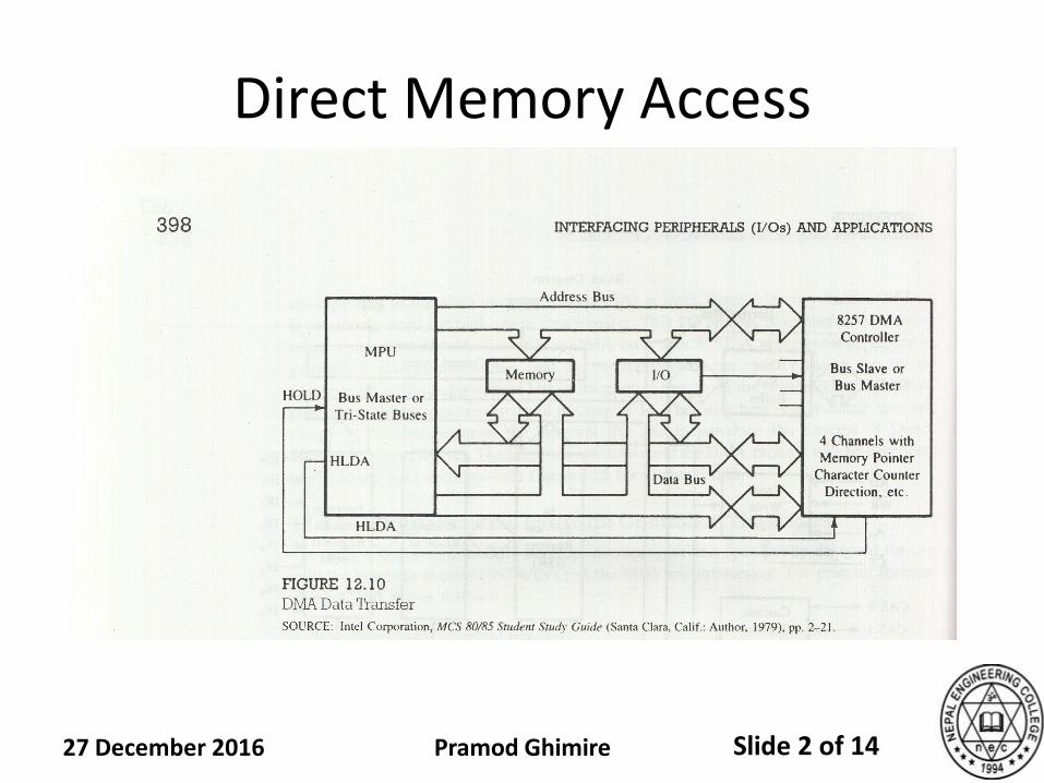
Direct Memory Access
27 December 2016 Pramod Ghimire
Slide 3 of 14
DMA Operation
Direct Memory Access (DMA) is an I/O technique commonly
used for high-speed data transfer; for example , data transfer
between memory and a floppy disk.
In DMA, µP releases the control of the buses to a device called
a DMA controller. The controller manages data transfer
between memory and a peripheral under its control, thus
bypassing the MPU
It introduces two new signals HOLD (pin 39) and HLDA (pin
38) (Hold acknowledge)
27 December 2016 Pramod Ghimire
Slide 4 of 14
HOLD
This is an active high input signal
Pin number 39
The processor relinquishes (gives up) the buses in the
following machine cycle once the MPU receives the HOLD
request
All buses are tri-stated and HLDA (Hold Acknowledge) signal
is sent out
MPU regains the control of the buses after HOLD goes low
27 December 2016 Pramod Ghimire
Slide 5 of 14
HLDA
This is an active high output signal
Pin number 38
It indicates that the MPU is giving up the control of the buses
27 December 2016 Pramod Ghimire

Slide 6 of 14
DMA Controller Essentials
The DMA controller should have
I. A data bus
II. An address bus
III. Read/Write control signals, and
IV. Control signals to disable its role as a peripheral and to
enable its role as a peripheral
(Note that DMA controller is a processor capable only of
copying data at high speed from one location to another
location)
27 December 2016 Pramod Ghimire
Slide 7 of 14
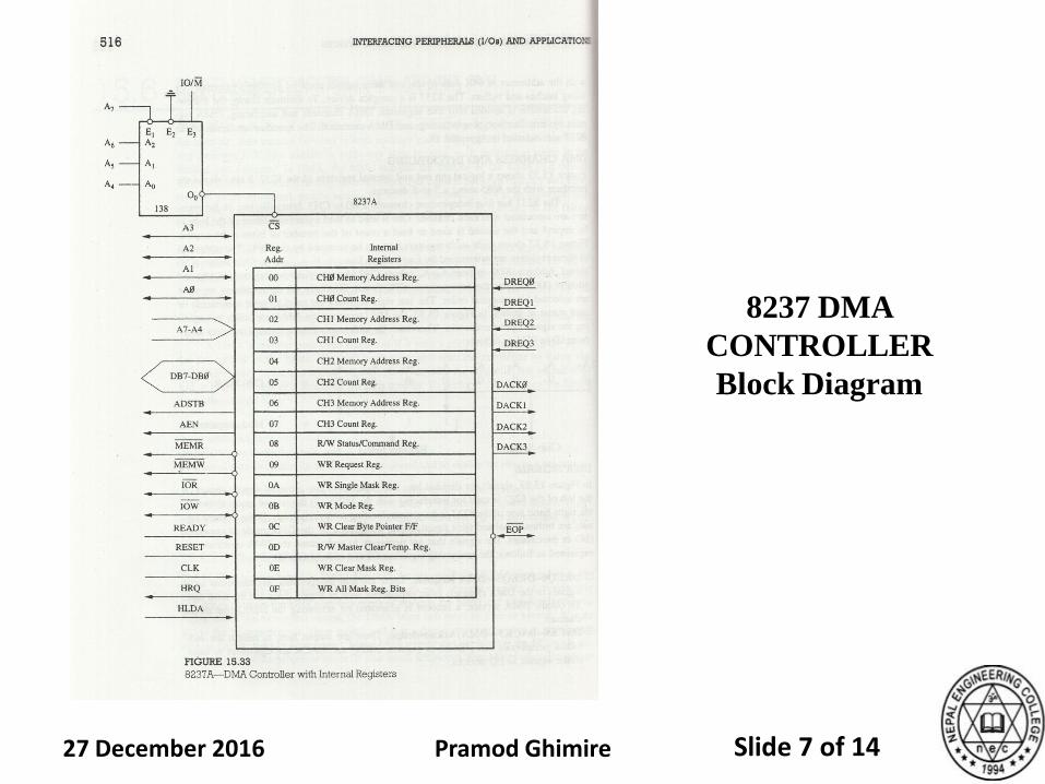
8237 DMA
CONTROLLER
Block Diagram
27 December 2016 Pramod Ghimire
Slide 8 of 14
Features
8237 is a programmable Direct Memory Access controller
(DMA) housed in a 40-pin package
It has four independent channels with each channel capable of
transferring 64K bytes
It must interface with MPU and a peripheral device
It is an I/O device to MPU
It is a data transfer processor to peripheral device
Many of its signals that are input in the I/O mode become
outputs in the processor mode
27 December 2016 Pramod Ghimire
Slide 9 of 14
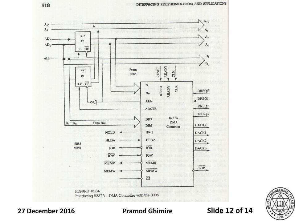
Description
The block diagram shows a logical pin out and internal registers of the 8237. It also shows the interface with the 8085 using a 3-to-8 decoder
8237 has four independent channels CH0-CH3. Two 16-bit registers are internally associated with each channel
These registers are determined by A3-A0 and the chip select line (CS)
The 8237 signals are divided into two groups:
1) signals on left (used to communicate with MPU)
2) signals on right (used to communicate with peripheral)
Some of these signals are bidirectional and are determined by the DMA mode of operation (I/O or processor mode)
27 December 2016 Pramod Ghimire
Slide 10 of 14
DMA Signals
To obtain DMA service , a request is generated by activating
the DREQ line of the channel
DACK are output lines to inform the individual peripherals
that DMA is granted. DREQ and DACK are eqvt to handshake
signals in I/O devices
AEN and ADSTB-Address Enable and Address Strobe are
used to latch a high-order byte to generate a 16-bit address
After receiving the HRQ (Hold request), the MPU completes
the bus cycle in process and issues the HLDA (Hold
Acknowledgement) signal
27 December 2016 Pramod Ghimire
Slide 11 of 14
System Interface
When a transfer begins, the DMA places the low-order byte on
the address bus and high-order byte on the data bus
Then 8237 asserts AEN (Address Enable) and ADSTB
(Address Strobe)
Theses two signals are used to latch the high-order byte from
the data bus and 8237 places the 16-bit address on the system
bus
27 December 2016 Pramod Ghimire
Slide 12 of 14 27 December 2016 Pramod Ghimire
Slide 13 of 14
NEXT CLASS
Serial Communication
(Chapter 16)
27 December 2016 Pramod Ghimire
Slide 14 of 14
THANK YOU
27 December 2016 Pramod Ghimire