8255 i/o programming - github pages•code assembly language instructions to read and write data to...
TRANSCRIPT

The x86 PC
Assembly Language, Design, and Interfacing
By Muhammad Ali Mazidi, Janice Gillespie Mazidi and Danny Causey
© 2010, 2003, 2000, 1998 Pearson Higher Education, Inc.
Pearson Prentice Hall - Upper Saddle River, NJ 07458
Chapter ELEVEN
8255 I/O PROGRAMMING

The x86 PC
Assembly Language, Design, and Interfacing
By Muhammad Ali Mazidi, Janice Gillespie Mazidi and Danny Causey
© 2010, 2003, 2000, 1998 Pearson Higher Education, Inc.
Pearson Prentice Hall - Upper Saddle River, NJ 07458
OBJECTIVES this chapter enables the student to:
• Code Assembly language instructions to read
and write data to and from I/O ports.
• Diagram the design of peripheral I/O using the
74LS373 output latch and the 74LS244 input buffer.
• Describe the I/O address map of x86 PCs.
• List the differences in memory-mapped I/O versus
peripheral I/O.
• Describe the purpose of the 8255 programmable
peripheral interface chip.

The x86 PC
Assembly Language, Design, and Interfacing
By Muhammad Ali Mazidi, Janice Gillespie Mazidi and Danny Causey
© 2010, 2003, 2000, 1998 Pearson Higher Education, Inc.
Pearson Prentice Hall - Upper Saddle River, NJ 07458
11.1: 8088 INPUT/OUTPUT INSTRUCTIONS
• All x86 processors, 8088 to Pentium®, can access
external devices called ports using I/O instructions.
– Memory can contain both Instructions and data.
– I/O ports contain data only
• Two instructions: “OUT” and “IN” send data from the
accumulator (AL or AX) to ports or bring data from
ports into the accumulator.
• 8088 I/O operation is applicable to all x86 CPUs.
– The 8-bit port uses the D0–D7 data bus for I/O devices.

The x86 PC
Assembly Language, Design, and Interfacing
By Muhammad Ali Mazidi, Janice Gillespie Mazidi and Danny Causey
© 2010, 2003, 2000, 1998 Pearson Higher Education, Inc.
Pearson Prentice Hall - Upper Saddle River, NJ 07458
11.1: 8088 INPUT/OUTPUT INSTRUCTIONS 8-bit data ports
• Register AL is used as the source/destination
for IN/OUT instructions.
– To input or output data from any other registers,
the data must first be moved to the AL register.
• Instructions OUT and IN have the following formats:
The x86 PC
Assembly Language, Design, and Interfacing
By Muhammad Ali Mazidi, Janice Gillespie Mazidi and Danny Causey
© 2010, 2003, 2000, 1998 Pearson Higher Education, Inc.
Pearson Prentice Hall - Upper Saddle River, NJ 07458
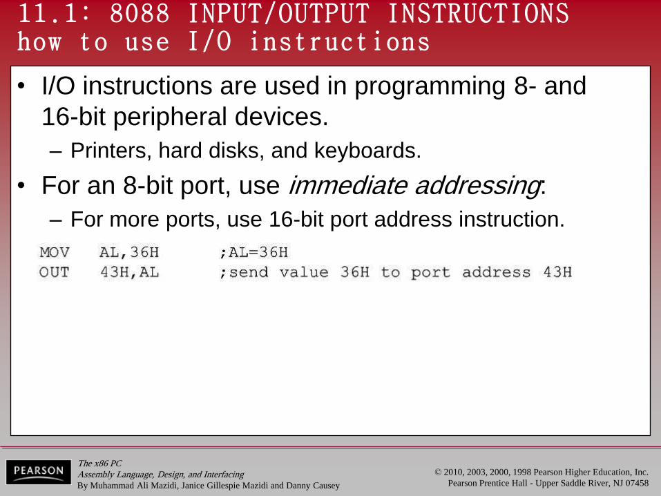
11.1: 8088 INPUT/OUTPUT INSTRUCTIONS how to use I/O instructions
• I/O instructions are used in programming 8- and
16-bit peripheral devices.
– Printers, hard disks, and keyboards.
• For an 8-bit port, use immediate addressing:
– For more ports, use 16-bit port address instruction.

The x86 PC
Assembly Language, Design, and Interfacing
By Muhammad Ali Mazidi, Janice Gillespie Mazidi and Danny Causey
© 2010, 2003, 2000, 1998 Pearson Higher Education, Inc.
Pearson Prentice Hall - Upper Saddle River, NJ 07458
11.1: 8088 INPUT/OUTPUT INSTRUCTIONS how to use I/O instructions
• 16-bit port address instruction using register indirect addressing mode with register DX.
– This program toggles port address 300H continuously.
– Only DX can be used for 16-bit I/O addresses.
– Use register AL for 8-bit data.

The x86 PC
Assembly Language, Design, and Interfacing
By Muhammad Ali Mazidi, Janice Gillespie Mazidi and Danny Causey
© 2010, 2003, 2000, 1998 Pearson Higher Education, Inc.
Pearson Prentice Hall - Upper Saddle River, NJ 07458
11.1: 8088 INPUT/OUTPUT INSTRUCTIONS how to use I/O instructions
Example 11-1 shows decision making
based on the data that was input.

The x86 PC
Assembly Language, Design, and Interfacing
By Muhammad Ali Mazidi, Janice Gillespie Mazidi and Danny Causey
© 2010, 2003, 2000, 1998 Pearson Higher Education, Inc.
Pearson Prentice Hall - Upper Saddle River, NJ 07458
11.2: I/O ADDRESS DECODING AND DESIGN
• The concept of address bus decoding for I/O
instructions is exactly the same as for memory.
– 1. The control signals IOR and IOW are used along
with the decoder.
– 2. For an 8-bit port address, A0–A7 is decoded.
– 3. If the port address is 16-bit (using DX), A0–A15
is decoded.

The x86 PC
Assembly Language, Design, and Interfacing
By Muhammad Ali Mazidi, Janice Gillespie Mazidi and Danny Causey
© 2010, 2003, 2000, 1998 Pearson Higher Education, Inc.
Pearson Prentice Hall - Upper Saddle River, NJ 07458
11.2: I/O ADDRESS DECODING AND DESIGN using 74LS373 in an output port design
• 74LS373 can be used as a
latching system for simple
I/O ports.
– Pin OC must be grounded.
Figure 11-1 74LS373 D Latch

The x86 PC
Assembly Language, Design, and Interfacing
By Muhammad Ali Mazidi, Janice Gillespie Mazidi and Danny Causey
© 2010, 2003, 2000, 1998 Pearson Higher Education, Inc.
Pearson Prentice Hall - Upper Saddle River, NJ 07458
11.2: I/O ADDRESS DECODING AND DESIGN using 74LS373 in an output port design
Figure 11-2 Design
for “OUT 99H, AL”.
• For an output latch, it is common to AND the output
of the address decoder with control signal IOW.
– To provide the latching action.

The x86 PC
Assembly Language, Design, and Interfacing
By Muhammad Ali Mazidi, Janice Gillespie Mazidi and Danny Causey
© 2010, 2003, 2000, 1998 Pearson Higher Education, Inc.
Pearson Prentice Hall - Upper Saddle River, NJ 07458
11.2: I/O ADDRESS DECODING AND DESIGN using 74LS373 in an output port design
Figure 11-3 Design for
Output Port Address 31H.

The x86 PC
Assembly Language, Design, and Interfacing
By Muhammad Ali Mazidi, Janice Gillespie Mazidi and Danny Causey
© 2010, 2003, 2000, 1998 Pearson Higher Education, Inc.
Pearson Prentice Hall - Upper Saddle River, NJ 07458
11.2: I/O ADDRESS DECODING AND DESIGN IN port design using 74LS244
• 74LS244 is widely used for buffering and providing
high driving capability for unidirectional buses.
Figure 11-5 Design for “IN AL, 9FH”
The address decoder & the IOR
control signal together activate
the tri-state input.

The x86 PC
Assembly Language, Design, and Interfacing
By Muhammad Ali Mazidi, Janice Gillespie Mazidi and Danny Causey
© 2010, 2003, 2000, 1998 Pearson Higher Education, Inc.
Pearson Prentice Hall - Upper Saddle River, NJ 07458
11.2: I/O ADDRESS DECODING AND DESIGN memory-mapped I/O
• Some processors do not have IN & OUT instructions,
but use Memory-mapped I/O.
– A memory location is assigned as an input or output port.
– Instructions access memory locations to access I/O ports.
• Instead of IN and OUT instructions.
– The entire 20-bit address, A0–A19, must be decoded.
• The DS register must be loaded prior to accessing
memory-mapped I/O.
– In memory-mapped I/O interfacing, control signals
MEMR and MEMW are used.
• Memory I/O ports can number as high as 220 (1,048,576).

The x86 PC
Assembly Language, Design, and Interfacing
By Muhammad Ali Mazidi, Janice Gillespie Mazidi and Danny Causey
© 2010, 2003, 2000, 1998 Pearson Higher Education, Inc.
Pearson Prentice Hall - Upper Saddle River, NJ 07458
11.2: I/O ADDRESS DECODING AND DESIGN memory-mapped I/O
• Some processors do not have IN & OUT instructions,
but use Memory-mapped I/O.
– Memory-mapped I/O can perform arithmetic & logic
operations on I/O data directly without first moving them
into the accumulator.
– Memory-mapped I/O uses memory address space, which
could lead to memory space fragmentation.
The x86 PC
Assembly Language, Design, and Interfacing
By Muhammad Ali Mazidi, Janice Gillespie Mazidi and Danny Causey
© 2010, 2003, 2000, 1998 Pearson Higher Education, Inc.
Pearson Prentice Hall - Upper Saddle River, NJ 07458
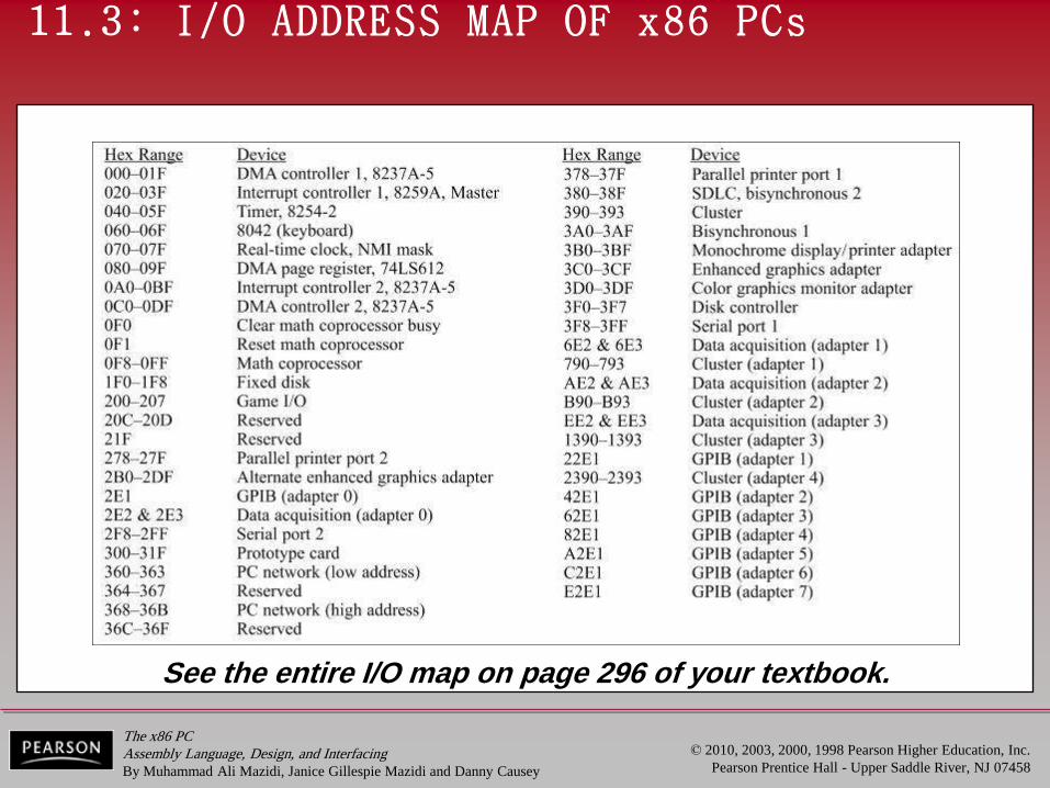
See the entire I/O map on page 296 of your textbook.
11.3: I/O ADDRESS MAP OF x86 PCs

The x86 PC
Assembly Language, Design, and Interfacing
By Muhammad Ali Mazidi, Janice Gillespie Mazidi and Danny Causey
© 2010, 2003, 2000, 1998 Pearson Higher Education, Inc.
Pearson Prentice Hall - Upper Saddle River, NJ 07458
11.3: I/O ADDRESS MAP OF x86 PCs absolute vs. linear address decoding
• In decoding addresses, either all or a selected
number of them are decoded.
– In absolute decoding, all address lines are decoded.
– If only selected address pins are decoded, it is called
linear select decoding.
• Linear select is cheaper, but creates aliases, the
same port with multiple addresses.
– If you see a large gap in the I/O address map of the x86
PC, it is due to the address aliases of the original PC.
The x86 PC
Assembly Language, Design, and Interfacing
By Muhammad Ali Mazidi, Janice Gillespie Mazidi and Danny Causey
© 2010, 2003, 2000, 1998 Pearson Higher Education, Inc.
Pearson Prentice Hall - Upper Saddle River, NJ 07458
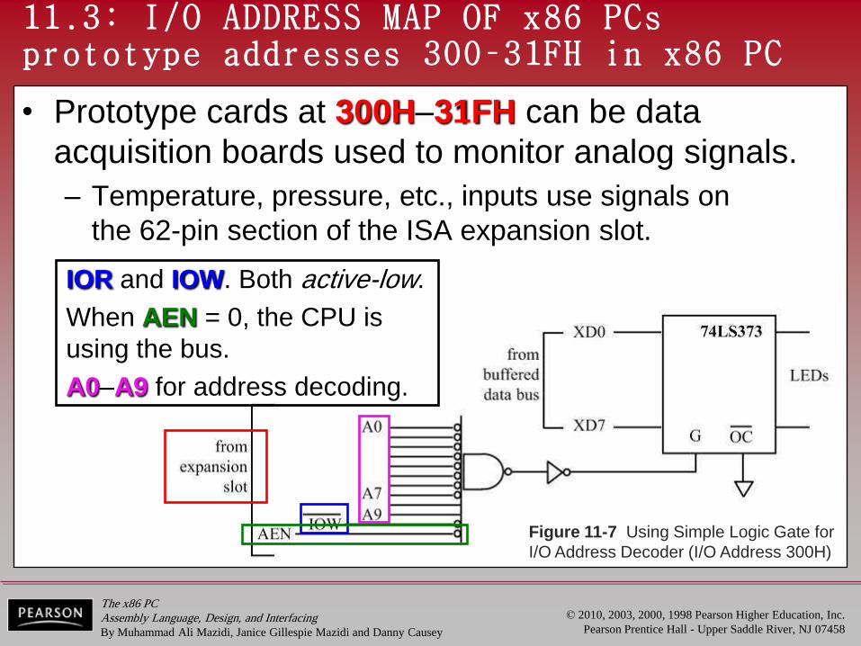
11.3: I/O ADDRESS MAP OF x86 PCs prototype addresses 300–31FH in x86 PC
• Prototype cards at 300H–31FH can be data
acquisition boards used to monitor analog signals.
– Temperature, pressure, etc., inputs use signals on
the 62-pin section of the ISA expansion slot.
Figure 11-7 Using Simple Logic Gate for
I/O Address Decoder (I/O Address 300H)
IOR and IOW. Both active-low.
When AEN = 0, the CPU is
using the bus.
A0–A9 for address decoding.

The x86 PC
Assembly Language, Design, and Interfacing
By Muhammad Ali Mazidi, Janice Gillespie Mazidi and Danny Causey
© 2010, 2003, 2000, 1998 Pearson Higher Education, Inc.
Pearson Prentice Hall - Upper Saddle River, NJ 07458
11.3: I/O ADDRESS MAP OF x86 PCs 74LS138 as a decoder
• NANDs, inverters, and 74LS138 chips for decoders
can be applied to I/O address decoding.
Figure 11-8 74S138 Decoder

The x86 PC
Assembly Language, Design, and Interfacing
By Muhammad Ali Mazidi, Janice Gillespie Mazidi and Danny Causey
© 2010, 2003, 2000, 1998 Pearson Higher Education, Inc.
Pearson Prentice Hall - Upper Saddle River, NJ 07458
11.3: I/O ADDRESS MAP OF x86 PCs 74LS138 as IBM PC I/O address decoder
– A0 to A4 go to individual peripheral input addresses.
– A5, A6, & A7 handle output selection of outputs Y0 to Y7.
– Pins A8, A9, & AEN all must be low to enable 74LS138.
• AEN is low only when the x86 is in control of the system bus.
Figure 11-10 PC/XT Port Address Coding
See table 11-2 on page 298 of your textbook.

The x86 PC
Assembly Language, Design, and Interfacing
By Muhammad Ali Mazidi, Janice Gillespie Mazidi and Danny Causey
© 2010, 2003, 2000, 1998 Pearson Higher Education, Inc.
Pearson Prentice Hall - Upper Saddle River, NJ 07458
Figure 11-11 8255 PPI Chip
11.4: PROGRAMMING & INTERFACING THE 8255
• The 8255 is a widely used
40-pin, DIP I/O chip.
– It has three separately accessible
programmed ports, A, B & C.
– Each port can be programmed
to be input or output.
– Ports can also be changed
dynamically.
These 8-bit
ports can
be all input
or all output.
Port A (PA0–PA7)
Port B (PB0–PB7)
Port C (PC0–PC7)

The x86 PC
Assembly Language, Design, and Interfacing
By Muhammad Ali Mazidi, Janice Gillespie Mazidi and Danny Causey
© 2010, 2003, 2000, 1998 Pearson Higher Education, Inc.
Pearson Prentice Hall - Upper Saddle River, NJ 07458
Figure 11-12 8255 Control
Word Format (I/O Mode)
11.4: PROGRAMMING & INTERFACING THE 8255 mode selection of the 8255A
• 8255 ports can be programmed in various modes. – The simple I/O mode, Mode 0, is most widely used.
Any of the ports
A, B, CL & CU
are programmable
as input or output.
All bits are out
or all are in.
No control of
individual bits

The x86 PC
Assembly Language, Design, and Interfacing
By Muhammad Ali Mazidi, Janice Gillespie Mazidi and Danny Causey
© 2010, 2003, 2000, 1998 Pearson Higher Education, Inc.
Pearson Prentice Hall - Upper Saddle River, NJ 07458
ENDS ; ELEVEN