a 1280x960 3.75um pixel cmos imager with triple exposure … workshops/2009 workshop/2009...
TRANSCRIPT
A 1280x960 3.75um pixel CMOS imager
with Triple Exposure HDR Johannes Solhusvik1, Sohrab Yaghmai1, Arthur Kimmels1, Christian
Stephansen1, Alf Storm1, Jenny Olsson1, Anders Rosnes1, Tore
Martinussen1, Trygve Willassen1, Per Olaf Pahr1, Siri Eikedal1, Steve
Shaw2, Ranjit Bhamra2, Sergey Velichko3, Dan Pates3, Sachin Datar3,
Scott Smith3, Lingtao Jiang3, Dave Wing3 , Ajaya Chilumula3 1Aptina Imaging, Oslo, Norway, 2Aptina Imaging, Bracknell, UK
3Aptina Imaging, San Jose, CA, USA
A triple exposure 20-bit output high dynamic range (HDR)
CMOS imager with sub 2e- rms noise floor is presented. The
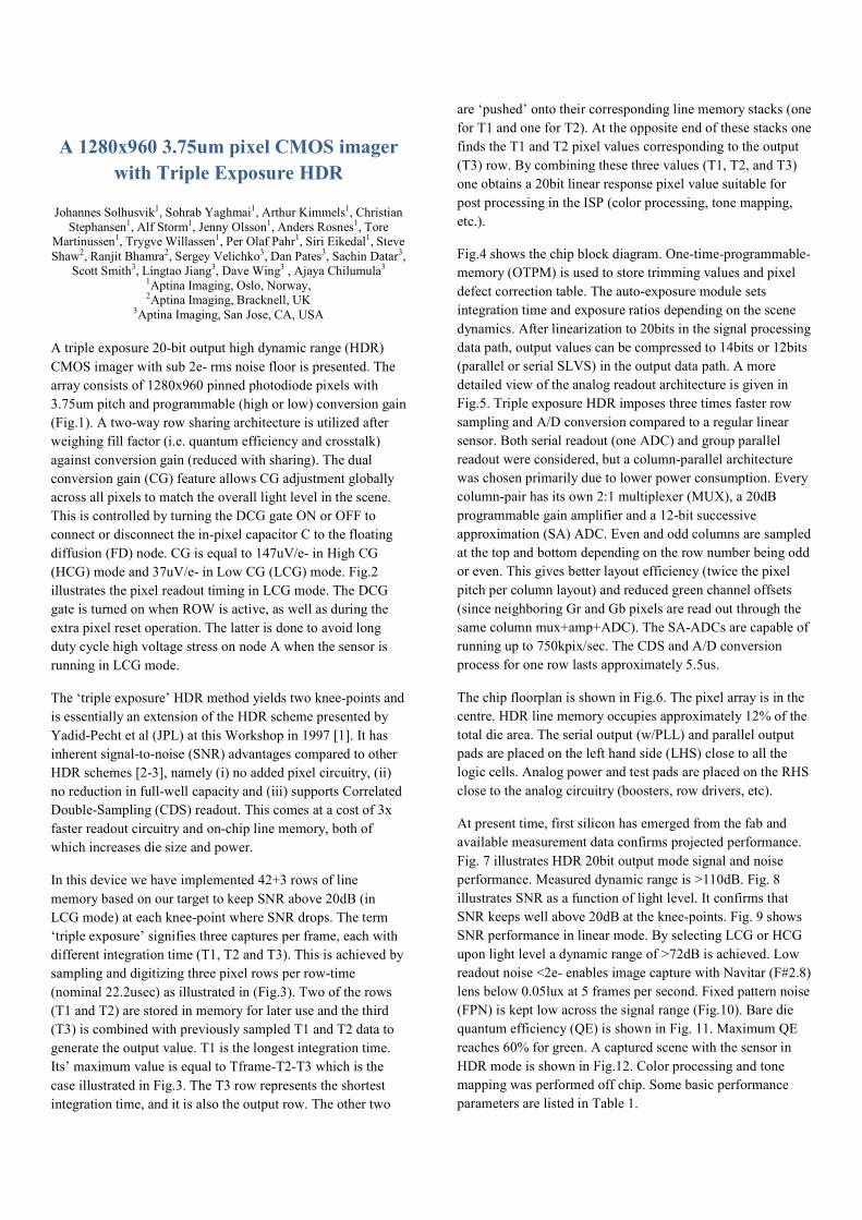
array consists of 1280x960 pinned photodiode pixels with
3.75um pitch and programmable (high or low) conversion gain
(Fig.1). A two-way row sharing architecture is utilized after
weighing fill factor (i.e. quantum efficiency and crosstalk)
against conversion gain (reduced with sharing). The dual
conversion gain (CG) feature allows CG adjustment globally
across all pixels to match the overall light level in the scene.
This is controlled by turning the DCG gate ON or OFF to
connect or disconnect the in-pixel capacitor C to the floating
diffusion (FD) node. CG is equal to 147uV/e- in High CG
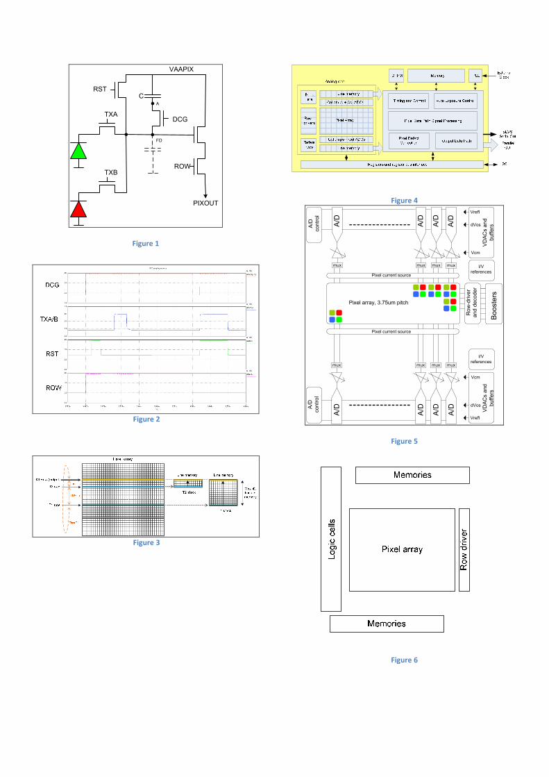
(HCG) mode and 37uV/e- in Low CG (LCG) mode. Fig.2
illustrates the pixel readout timing in LCG mode. The DCG
gate is turned on when ROW is active, as well as during the
extra pixel reset operation. The latter is done to avoid long
duty cycle high voltage stress on node A when the sensor is
running in LCG mode.
The ‘triple exposure’ HDR method yields two knee-points and
is essentially an extension of the HDR scheme presented by
Yadid-Pecht et al (JPL) at this Workshop in 1997 [1]. It has
inherent signal-to-noise (SNR) advantages compared to other
HDR schemes [2-3], namely (i) no added pixel circuitry, (ii)
no reduction in full-well capacity and (iii) supports Correlated
Double-Sampling (CDS) readout. This comes at a cost of 3x
faster readout circuitry and on-chip line memory, both of
which increases die size and power.
In this device we have implemented 42+3 rows of line
memory based on our target to keep SNR above 20dB (in
LCG mode) at each knee-point where SNR drops. The term
‘triple exposure’ signifies three captures per frame, each with
different integration time (T1, T2 and T3). This is achieved by
sampling and digitizing three pixel rows per row-time
(nominal 22.2usec) as illustrated in (Fig.3). Two of the rows
(T1 and T2) are stored in memory for later use and the third
(T3) is combined with previously sampled T1 and T2 data to
generate the output value. T1 is the longest integration time.
Its’ maximum value is equal to Tframe-T2-T3 which is the
case illustrated in Fig.3. The T3 row represents the shortest
integration time, and it is also the output row. The other two
are ‘pushed’ onto their corresponding line memory stacks (one
for T1 and one for T2). At the opposite end of these stacks one
finds the T1 and T2 pixel values corresponding to the output
(T3) row. By combining these three values (T1, T2, and T3)
one obtains a 20bit linear response pixel value suitable for
post processing in the ISP (color processing, tone mapping,
etc.).
Fig.4 shows the chip block diagram. One-time-programmable-
memory (OTPM) is used to store trimming values and pixel
defect correction table. The auto-exposure module sets
integration time and exposure ratios depending on the scene
dynamics. After linearization to 20bits in the signal processing
data path, output values can be compressed to 14bits or 12bits
(parallel or serial SLVS) in the output data path. A more
detailed view of the analog readout architecture is given in
Fig.5. Triple exposure HDR imposes three times faster row
sampling and A/D conversion compared to a regular linear
sensor. Both serial readout (one ADC) and group parallel
readout were considered, but a column-parallel architecture
was chosen primarily due to lower power consumption. Every
column-pair has its own 2:1 multiplexer (MUX), a 20dB
programmable gain amplifier and a 12-bit successive
approximation (SA) ADC. Even and odd columns are sampled
at the top and bottom depending on the row number being odd
or even. This gives better layout efficiency (twice the pixel
pitch per column layout) and reduced green channel offsets
(since neighboring Gr and Gb pixels are read out through the
same column mux+amp+ADC). The SA-ADCs are capable of
running up to 750kpix/sec. The CDS and A/D conversion
process for one row lasts approximately 5.5us.
The chip floorplan is shown in Fig.6. The pixel array is in the
centre. HDR line memory occupies approximately 12% of the
total die area. The serial output (w/PLL) and parallel output
pads are placed on the left hand side (LHS) close to all the
logic cells. Analog power and test pads are placed on the RHS
close to the analog circuitry (boosters, row drivers, etc).
At present time, first silicon has emerged from the fab and
available measurement data confirms projected performance.
Fig. 7 illustrates HDR 20bit output mode signal and noise
performance. Measured dynamic range is >110dB. Fig. 8
illustrates SNR as a function of light level. It confirms that
SNR keeps well above 20dB at the knee-points. Fig. 9 shows
SNR performance in linear mode. By selecting LCG or HCG
upon light level a dynamic range of >72dB is achieved. Low
readout noise <2e- enables image capture with Navitar (F#2.8)
lens below 0.05lux at 5 frames per second. Fixed pattern noise
(FPN) is kept low across the signal range (Fig.10). Bare die
quantum efficiency (QE) is shown in Fig. 11. Maximum QE
reaches 60% for green. A captured scene with the sensor in
HDR mode is shown in Fig.12. Color processing and tone
mapping was performed off chip. Some basic performance
parameters are listed in Table 1.
RSTC
DCGTXA
ROW
PIXOUT
VAAPIX
TXB
A
FD
Figure 1
Figure 2
Figure 3
Figure 4
Pixel array, 3.75um pitch
I/V
references
Vref1
dVos
Vcm
Vref1
dVos
Vcm
Pixel current source
A/D
mux
A/D
mux
A/D
mux
A/D
mux
A/D
mux
A/D
mux
A/D
mux
A/D
control
A/D
control
Pixel current source
I/V
references
Boosters
Row-driver
and decoder
VDACs and
buffers
VDACs and
buffersA/D
mux
Figure 5
Figure 6
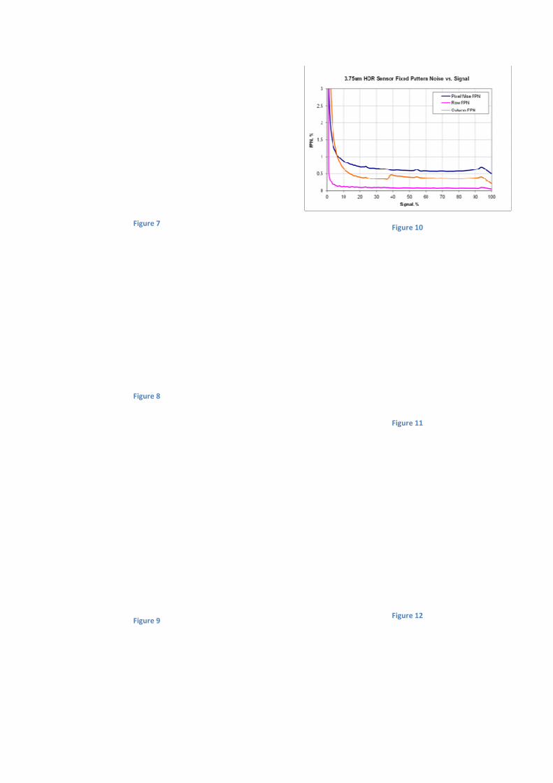
Figure 7
Figure 8
Figure 9
Figure 10
Figure 11
Figure 12
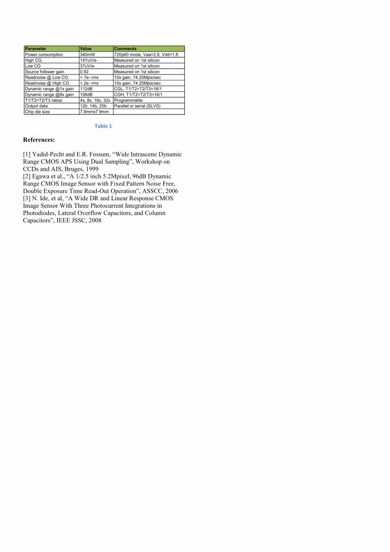
Table 1
References:
[1] Yadid-Pecht and E.R. Fossum, “Wide Intrascene Dynamic
Range CMOS APS Using Dual Sampling”, Workshop on
CCDs and AIS, Bruges, 1999
[2] Egawa et al., “A 1/2.5 inch 5.2Mpixel, 96dB Dynamic
Range CMOS Image Sensor with Fixed Pattern Noise Free,
Double Exposure Time Read-Out Operation”, ASSCC, 2006
[3] N. Ide, et al, “A Wide DR and Linear Response CMOS
Image Sensor With Three Photocurrent Integrations in
Photodiodes, Lateral Overflow Capacitors, and Column
Capacitors”, IEEE JSSC, 2008
Parameter Value Comments
Power consumption 340mW 720p60 mode, Vaa=2.8, Vdd=1.8
High CG 147uV/e- Measured on 1st silicon
Low CG 37uV/e- Measured on 1st silicon
Source follower gain 0.92 Measured on 1st silicon
Readnoise @ Low CG < 7e- rms 10x gain, 74.25Mpix/sec
Readnoise @ High CG < 2e- rms 10x gain, 74.25Mpix/sec
Dynamic range @1x gain 112dB CGL, T1/T2=T2/T3=16/1
Dynamic range @8x gain 106dB CGH, T1/T2=T2/T3=16/1
T1/T2=T2/T3 ratios 4x, 8x, 16x, 32x Programmable
Output data 12b, 14b, 20b Parallel or serial (SLVS)
Chip die size 7.9mmx7.9mm