a 14-bit, 80 msps a/d converter ad6645
TRANSCRIPT

a
Information furnished by Analog Devices is believed to be accurate andreliable. However, no responsibility is assumed by Analog Devices for itsuse, nor for any infringements of patents or other rights of third parties thatmay result from its use. No license is granted by implication or otherwiseunder any patent or patent rights of Analog Devices.
One Technology Way, P.O. Box 9106, Norwood, MA 02062-9106, U.S.A.
Tel: 781/329-4700 www.analog.com
Fax: 781/326-8703 © Analog Devices, Inc., 2002
AD6645
14-Bit, 80 MSPSA/D Converter
REV. 0
FEATURES
80 MSPS Guaranteed Sample Rate
SNR = 75 dB, fIN 15 MHz @ 80 MSPS
SNR = 72 dB, fIN 200 MHz @ 80 MSPS
SFDR = 89 dBc, fIN 70 MHz @ 80 MSPS
100 dB Multitone SFDR
IF Sampling to 200 MHz
Sampling Jitter 0.1 ps
1.5 W Power Dissipation
Differential Analog Inputs
Pin-Compatible to AD6644
Two’s Complement Digital Output Format
3.3 V CMOS-Compatible
DataReady for Output Latching
APPLICATIONS
Multichannel, Multimode Receivers
Base Station Infrastructure
AMPS, IS-136, CDMA, GSM, WCDMA
Single Channel Digital Receivers
Antenna Array Processing
Communications Instrumentation
Radar, Infrared Imaging
Instrumentation
PRODUCT DESCRIPTIONThe AD6645 is a high-speed, high-performance, monolithic14-bit analog-to-digital converter. All necessary functions,including track-and-hold (T/H) and reference, are included onthe chip to provide a complete conversion solution. The AD6645provides CMOS-compatible digital outputs. It is the fourth
generation in a wideband ADC family, preceded by theAD9042 (12-bit, 41 MSPS), the AD6640 (12-bit, 65 MSPS,IF sampling), and the AD6644 (14-bit, 40 MSPS/65 MSPS).
Designed for multichannel, multimode receivers, the AD6645 ispart of Analog Device’s SoftCell™ transceiver chipset. TheAD6645 maintains 100 dB multitone, spurious-free dynamicrange (SFDR) through the second Nyquist band. This break-through performance eases the burden placed on multimodedigital receivers (software radios) that are typically limited bythe ADC. Noise performance is exceptional; typical signal-to-noise ratio is 74.5 dB through the first Nyquist band.
The AD6645 is built on Analog Devices’ high-speed complemen-tary bipolar process (XFCB) and uses an innovative, multipasscircuit architecture. Units are available in a thermally enhanced 52-lead PowerQuad 4® (LQFP_ED) specified from –40∞C to +85∞C.
PRODUCT HIGHLIGHTS1. IF Sampling
The AD6645 maintains outstanding ac performance up toinput frequencies of 200 MHz. Suitable for multicarrier 3Gwideband cellular IF sampling receivers.
2. Pin CompatibilityThe ADC has the same footprint and pin layout as theAD6644, 14-Bit 40 MSPS/65 MSPS ADC.
3. SFDR Performance and OversamplingMultitone SFDR performance of –100 dBc can reduce therequirements of high-end RF components and allows the useof receive signal processors such as the AD6620 or AD6624/AD6624A.
FUNCTIONAL BLOCK DIAGRAM
5
A1 TH2 A2 TH4 ADC3TH5TH3TH1
DAC1 ADC2 DAC2ADC1 6
AIN
AIN
VREF
ENCODE
ENCODE
AVCC DVCC
GND DMID OVR DRY D13MSB
D12 D11 D10 D9 D8 D7 D6 D5 D4 D3 D2 D1 D0LSB
INTERNALTIMING
5
DIGITAL ERROR CORRECTION LOGIC
AD6645
2.4V
SoftCell is a trademark of Analog Devices, Inc.PowerQuad 4 is a registered trademark of Amkor Technology, Inc.

REV. 0–2–
AD6645DC SPECIFICATIONS
AD6645ASQ-80Parameter Temp Test Level Min Typ Max Unit
RESOLUTION 14 Bits
ACCURACYNo Missing Codes Full II GuaranteedOffset Error Full II –10 +1.2 +10 mVGain Error Full II –10 0 +10 % FSDifferential Nonlinearity (DNL) Full II –1.0 ± 0.25 +1.5 LSBIntegral Nonlinearity (INL) Full V ± 0.5 LSB
TEMPERATURE DRIFTOffset Error Full V 1.5 ppm/∞CGain Error Full V 48 ppm/∞C
POWER SUPPLY REJECTION (PSRR) 25∞C V ± 1.0 mV/V
REFERENCE OUT (VREF)1 Full V 2.4 V
ANALOG INPUTS (AIN, AIN)Differential Input Voltage Range Full V 2.2 V p-pDifferential Input Resistance Full V 1 kWDifferential Input Capacitance 25∞C V 1.5 pF
POWER SUPPLYSupply Voltages
AVCC Full II 4.75 5.0 5.25 VDVCC Full II 3.0 3.3 3.6 V
Supply CurrentI AVCC (AVCC = 5.0 V) Full II 275 320 mAI DVCC (DVCC = 3.3 V) Full II 32 45 mA
Rise Time2
AVCC Full IV TBD ms
POWER CONSUMPTION Full II 1.5 1.75 W
NOTES1VREF is provided for setting the common-mode offset of a differential amplifier such as the AD8138 when a dc-coupled analog input is required. VREF should bebuffered if used to drive additional circuit functions.2Specified for dc supplies with linear rise-time characteristics. The use of dc supplies with linear rise-times of <45 ms is highly recommended.
Specifications subject to change without notice
DIGITAL SPECIFICATIONSAD6645ASQ-80
Parameter (Conditions) Temp Test Level Min Typ Max Unit
ENCODE INPUTS (ENC, ENC)Differential Input Voltage1 Full IV 0.4 V p-pDifferential Input Resistance 25∞C V 10 kWDifferential Input Capacitance 25∞C V 2.5 pF
LOGIC OUTPUTS (D13–D0, DRY, OVR2)Logic Compatibility CMOSLogic “1” Voltage (DVCC = 3.3 V)3 Full II 2.85 DVCC – 0.2 VLogic “0” Voltage (DVCC = 3.3 V)3 Full II 0.2 0.5 VOutput Coding Two’s ComplementDMID Full V DVCC/2 V
NOTES1All ac specifications tested by driving ENCODE and ENCODE differentially.2The functionality of the Over-Range bit is specified for a temperature range of 25∞C to 85∞C only.3Digital output logic levels: DVCC = 3.3 V, CLOAD = 10 pF. Capacitive loads >10 pF will degrade performance.
Specifications subject to change without notice.
(AVCC = 5 V, DVCC = 3.3 V; TMIN = –40�C, TMAX = +85�C, unless otherwise noted.)
(AVCC = 5 V, DVCC = 3.3 V; TMIN = –40�C, TMAX = +85�C, unless otherwise noted.)
–SPECIFICATIONS
REV. 0 –3–
AD6645
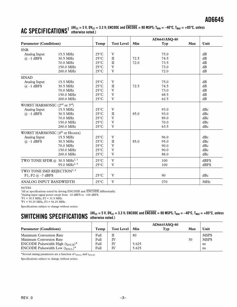
AC SPECIFICATIONS1
AD6645ASQ-80Parameter (Conditions) Temp Test Level Min Typ Max Unit
SNRAnalog Input 15.5 MHz 25∞C V 75.0 dB@ –1 dBFS 30.5 MHz 25∞C II 72.5 74.5 dB
70.0 MHz 25∞C II 72.0 73.5 dB150.0 MHz 25∞C V 73.0 dB200.0 MHz 25∞C V 72.0 dB
SINADAnalog Input 15.5 MHz 25∞C V 75.0 dB@ –1 dBFS 30.5 MHz 25∞C II 72.5 74.5 dB
70.0 MHz 25∞C V 73.0 dB150.0 MHz 25∞C V 68.5 dB200.0 MHz 25∞C V 62.5 dB
WORST HARMONIC (2nd or 3rd)Analog Input 15.5 MHz 25∞C V 93.0 dBc@ –1 dBFS 30.5 MHz 25∞C II 85.0 93.0 dBc
70.0 MHz 25∞C V 89.0 dBc150.0 MHz 25∞C V 70.0 dBc200.0 MHz 25∞C V 63.5 dBc
WORST HARMONIC (4th or HIGHER)Analog Input 15.5 MHz 25∞C V 96.0 dBc@ –1 dBFS 30.5 MHz 25∞C II 85.0 95.0 dBc
70.0 MHz 25∞C V 90.0 dBc150.0 MHz 25∞C V 90.0 dBc200.0 MHz 25∞C V 88.0 dBc
TWO TONE SFDR @ 30.5 MHz2, 3 25∞C V 100 dBFS55.0 MHz2, 4 25∞C V 100 dBFS
TWO TONE IMD REJECTION3, 4
F1, F2 @ –7 dBFS 25∞C V 90 dBc
ANALOG INPUT BANDWIDTH 25∞C V 270 MHz
NOTES1All ac specifications tested by driving ENCODE and ENCODE differentially.2Analog input signal power swept from –10 dBFS to –100 dBFS.3F1 = 30.5 MHz, F2 = 31.5 MHz.4F1 = 55.25 MHz, F2 = 56.25 MHz.
Specifications subject to change without notice.
SWITCHING SPECIFICATIONSAD6645ASQ-80
Parameter (Conditions) Temp Test Level Min Typ Max Unit
Maximum Conversion Rate Full II 80 MSPSMinimum Conversion Rate Full IV 30 MSPSENCODE Pulsewidth High (tENCH)* Full IV 5.625 nsENCODE Pulsewidth Low (tENCL)* Full IV 5.625 ns
*Several timing parameters are a function of tENCL and tENCH.
Specifications subject to change without notice.
(AVCC = 5 V, DVCC = 3.3 V; ENCODE and ENCODE = 80 MSPS; TMIN = –40�C, TMAX = +85�C, unlessotherwise noted.)
(AVCC = 5 V, DVCC = 3.3 V; ENCODE and ENCODE = 80 MSPS; TMIN = –40�C, TMAX = +85�C, unlessotherwise noted.)
REV. 0
AD6645
–4–
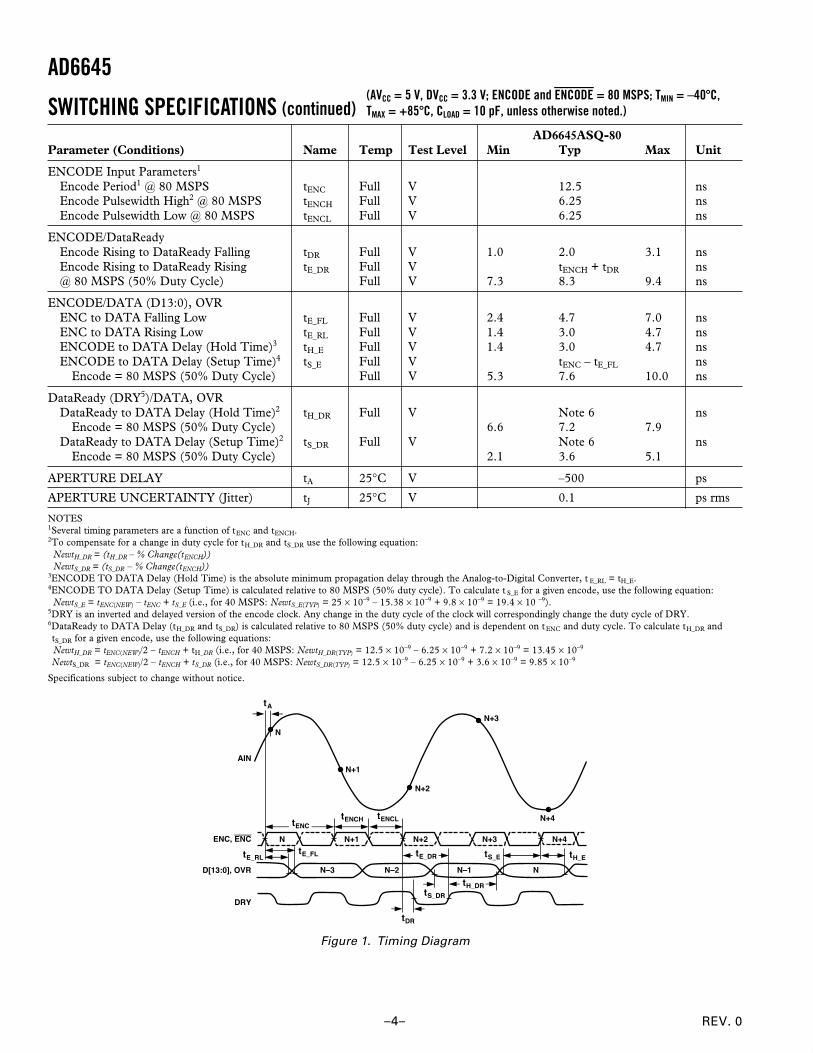
SWITCHING SPECIFICATIONS (continued) AD6645ASQ-80
Parameter (Conditions) Name Temp Test Level Min Typ Max Unit
ENCODE Input Parameters1
Encode Period1 @ 80 MSPS tENC Full V 12.5 nsEncode Pulsewidth High2 @ 80 MSPS tENCH Full V 6.25 nsEncode Pulsewidth Low @ 80 MSPS tENCL Full V 6.25 ns
ENCODE/DataReadyEncode Rising to DataReady Falling tDR Full V 1.0 2.0 3.1 nsEncode Rising to DataReady Rising tE_DR Full V tENCH + tDR ns@ 80 MSPS (50% Duty Cycle) Full V 7.3 8.3 9.4 ns
ENCODE/DATA (D13:0), OVRENC to DATA Falling Low tE_FL Full V 2.4 4.7 7.0 nsENC to DATA Rising Low tE_RL Full V 1.4 3.0 4.7 nsENCODE to DATA Delay (Hold Time)3 tH_E Full V 1.4 3.0 4.7 nsENCODE to DATA Delay (Setup Time)4 tS_E Full V tENC – tE_FL ns
Encode = 80 MSPS (50% Duty Cycle) Full V 5.3 7.6 10.0 ns
DataReady (DRY5)/DATA, OVRDataReady to DATA Delay (Hold Time)2 tH_DR Full V Note 6 ns
Encode = 80 MSPS (50% Duty Cycle) 6.6 7.2 7.9DataReady to DATA Delay (Setup Time)2 tS_DR Full V Note 6 ns
Encode = 80 MSPS (50% Duty Cycle) 2.1 3.6 5.1
APERTURE DELAY tA 25∞C V –500 ps
APERTURE UNCERTAINTY (Jitter) tJ 25∞C V 0.1 ps rms
NOTES1Several timing parameters are a function of tENC and tENCH.2To compensate for a change in duty cycle for tH_DR and tS_DR use the following equation: NewtH_DR = (tH_DR – % Change(tENCH)) NewtS_DR = (tS_DR – % Change(tENCH))3ENCODE TO DATA Delay (Hold Time) is the absolute minimum propagation delay through the Analog-to-Digital Converter, t E_RL = tH_E.4ENCODE TO DATA Delay (Setup Time) is calculated relative to 80 MSPS (50% duty cycle). To calculate t S_E for a given encode, use the following equation: NewtS_E = tENC(NEW) – tENC + tS_E (i.e., for 40 MSPS: NewtS_E(TYP) = 25 ¥ 10–9 – 15.38 ¥ 10–9 + 9.8 ¥ 10–9 = 19.4 ¥ 10 –9).5DRY is an inverted and delayed version of the encode clock. Any change in the duty cycle of the clock will correspondingly change the duty cycle of DRY.6DataReady to DATA Delay (tH_DR and tS_DR) is calculated relative to 80 MSPS (50% duty cycle) and is dependent on tENC and duty cycle. To calculate tH_DR andtS_DR for a given encode, use the following equations:
NewtH_DR = tENC(NEW)/2 – tENCH + tH_DR (i.e., for 40 MSPS: NewtH_DR(TYP) = 12.5 ¥ 10–9 – 6.25 ¥ 10–9 + 7.2 ¥ 10–9 = 13.45 ¥ 10–9
NewtS_DR = tENC(NEW)/2 – tENCH + tS_DR (i.e., for 40 MSPS: NewtS_DR(TYP) = 12.5 ¥ 10–9 – 6.25 ¥ 10–9 + 3.6 ¥ 10–9 = 9.85 ¥ 10–9
Specifications subject to change without notice.
tS_DR
tA
AIN
N
N+1
N+2
N+3
N+4 tENC tENCH tENCL
tE_FL tE_RL tE_DR tS_E tH_E
tDR
tH_DR
N N+1 N+2 N+3 N+4
NN�1N�2N�3
ENC, ENC
D[13:0], OVR
DRY
Figure 1. Timing Diagram
(AVCC = 5 V, DVCC = 3.3 V; ENCODE and ENCODE = 80 MSPS; TMIN = –40�C,TMAX = +85�C, CLOAD = 10 pF, unless otherwise noted.)
REV. 0 –5–
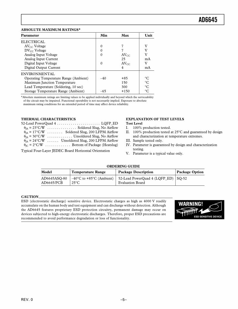
AD6645ABSOLUTE MAXIMUM RATINGS*
Parameter Min Max Unit
ELECTRICALAVCC Voltage 0 7 VDVCC Voltage 0 7 VAnalog Input Voltage 0 AVCC VAnalog Input Current 25 mADigital Input Voltage 0 AVCC VDigital Output Current 4 mA
ENVIRONMENTALOperating Temperature Range (Ambient) –40 +85 ∞CMaximum Junction Temperature 150 ∞CLead Temperature (Soldering, 10 sec) 300 ∞CStorage Temperature Range (Ambient) –65 +150 ∞C
THERMAL CHARACTERISTICS52-Lead PowerQuad 4 . . . . . . . . . . . . . . . . . . . . . . LQFP_ED �JA = 23∞C/W . . . . . . . . . . . . . . . Soldered Slug, No Airflow �JA = 17∞C/W . . . . . . . . Soldered Slug, 200 LFPM Airflow �JA = 30∞C/W . . . . . . . . . . . . . Unsoldered Slug, No Airflow �JA = 24∞C/W . . . . . . Unsoldered Slug, 200 LFPM Airflow �JC = 2∞C/W . . . . . . . . . . . . . Bottom of Package (Heatslug)
Typical Four-Layer JEDEC Board Horizontal Orientation
CAUTIONESD (electrostatic discharge) sensitive device. Electrostatic charges as high as 4000 V readilyaccumulate on the human body and test equipment and can discharge without detection. Althoughthe AD6645 features proprietary ESD protection circuitry, permanent damage may occur ondevices subjected to high-energy electrostatic discharges. Therefore, proper ESD precautions arerecommended to avoid performance degradation or loss of functionality.
WARNING!
ESD SENSITIVE DEVICE
EXPLANATION OF TEST LEVELSTest LevelI. 100% production tested.II. 100% production tested at 25∞C and guaranteed by design
and characterization at temperature extremes.III. Sample tested only.IV. Parameter is guaranteed by design and characterization
testing.V. Parameter is a typical value only.
*Absolute maximum ratings are limiting values to be applied individually and beyond which the serviceabilityof the circuit may be impaired. Functional operability is not necessarily implied. Exposure to absolutemaximum rating conditions for an extended period of time may affect device reliability.
ORDERING GUIDE
Model Temperature Range Package Description Package Option
AD6645ASQ-80 –40∞C to +85∞C (Ambient) 52-Lead PowerQuad 4 (LQFP_ED) SQ-52AD6645/PCB 25∞C Evaluation Board

REV. 0
AD6645
–6–
PIN CONFIGURATION
52 51 50 49 48 43 42 41 4047 46 45 44
14 15 16 17 18 19 20 21 22 23 24 25 26
1
2
3
4
5
6
7
8
9
10
11
13
12
PIN 1IDENTIFIER
TOP VIEW(Not to Scale)
39
38
37
36
35
34
33
32
31
30
29
28
27
AD6645
AV
CC
GN
D
AV
CC
GN
D
AV
CC
GN
D
GN
D
AV
CC
GN
D C2
GN
D
AV
CC
DR
YD
13 (
MS
B)
D12
D11
D10
D9
D8
D7
DV
CC
GN
D
D5
D4
DVCCGND
VREF
GND
ENC
ENC
GND
AVCCAVCCGND
AIN
AIN
GND
D3
D2
D1
D0 (LSB)
DMID
GND
DVCCOVR
DNC
AVCCGND
AVCCGND
C1
D6
DNC = DO NOT CONNECT
PIN FUNCTION DESCRIPTIONS
Pin No. Mnemonic Function
1, 33, 43 DVCC 3.3 V Power Supply (Digital) Output Stage Only
2, 4, 7, 10, 13, GND Ground15, 17, 19, 21,23, 25, 27, 29,34, 42
3 VREF 2.4 V Reference. Bypass to ground with a 0.1 mF microwave chip capacitor.
5 ENC Encode Input. Conversion initiated on rising edge.
6 ENC Complement of ENC, Differential Input
8, 9, 14, 16, 18, AVCC 5 V Analog Power Supply22, 26, 28, 30
11 AIN Analog Input
12 AIN Complement of AIN, Differential Analog Input
20 C1 Internal Voltage Reference. Bypass to ground with a 0.1 mF chip capacitor.
24 C2 Internal Voltage Reference. Bypass to ground with a 0.1 mF chip capacitor.
31 DNC Do not connect this pin.
32 OVR* Over-Range Bit. A logic-level high indicates analog input exceeds ± FS.
35 DMID Output Data Voltage Midpoint. Approximately equal to (DVCC)/2.
36 D0 (LSB) Digital Output Bit (Least Significant Bit); Two’s Complement
37–41, 44–50 D1–D5, D6–D12 Digital Output Bits in Two’s Complement
51 D13 (MSB) Digital Output Bit (Most Significant Bit); Two’s Complement
52 DRY DataReady Output
*The functionality of the Over-Range bit is specified for a temperature range of 25∞C to 85∞C only.

REV. 0 –7–
AD6645DEFINITIONS OF SPECIFICATIONSAnalog BandwidthThe analog input frequency at which the spectral power of thefundamental frequency (as determined by the FFT analysis) isreduced by 3 dB.
Aperture DelayThe delay between the 50% point of the rising edge of theENCODE command and the instant at which the analog inputis sampled.
Aperture Uncertainty (Jitter)The sample-to-sample variation in aperture delay.
Differential Analog Input Resistance, Differential AnalogInput Capacitance, and Differential Analog Input ImpedanceThe real and complex impedances measured at each analoginput port. The resistance is measured statically and the capaci-tance and differential input impedances are measured with anetwork analyzer.
Differential Analog Input Voltage RangeThe peak-to-peak differential voltage that must be applied tothe converter to generate a full-scale response. Peak differentialvoltage is computed by observing the voltage on a single pin andsubtracting the voltage from the other pin, which is 180 degreesout of phase. Peak-to-peak differential is computed by rotatingthe inputs phase 180 degrees and taking the peak measurementagain. Then the difference is computed between both peakmeasurements.
Differential NonlinearityThe deviation of any code width from an ideal 1 LSB step.
Encode Pulsewidth/Duty CyclePulsewidth high is the minimum amount of time that theENCODE pulse should be left in Logic “1” state to achieverated performance; pulsewidth low is the minimum timeENCODE pulse should be left in low state. See timing implica-tions of changing tENCH in text. At a given clock rate, thesespecs define an acceptable ENCODE duty cycle.
Full-Scale Input PowerExpressed in dBm. Computed using the following equation:
Power
VZ
Full Scale
Full Scale rms
Input=
È
Î
ÍÍÍÍÍ
ù
û
úúúúú
100 001
2
log| |
.
Harmonic Distortion, 2nd
The ratio of the rms signal amplitude to the rms value of thesecond harmonic component, reported in dBc.
Harmonic Distortion, 3rd
The ratio of the rms signal amplitude to the rms value of thethird harmonic component, reported in dBc.
Integral NonlinearityThe deviation of the transfer function from a reference linemeasured in fractions of 1 LSB using a “best straight line”determined by a least square curve fit.
Minimum Conversion RateThe encode rate at which the SNR of the lowest analogsignal frequency drops by no more than 3 dB below theguaranteed limit.
Maximum Conversion RateThe encode rate at which parametric testing is performed.
Noise (For Any Range Within the ADC)
V ZNOISE
FS SNR SignaldBm dBc dBFS
= ¥ ¥-Ê
ËÁ��̄
| | .–
0 001 10 10
Where Z is the input impedance, FS is the full scale of the devicefor the frequency in question; SNR is the value for the particularinput level; and Signal is the signal level within the ADC reportedin dB below full scale. This value includes both thermal andquantization noise.
Output Propagation DelayThe delay between a differential crossing of ENCODE andENCODE and the time when all output data bits are withinvalid logic levels.
Power Supply Rejection RatioThe ratio of a change in input offset voltage to a change in powersupply voltage.
Power Supply Rise TimeThe time from when the dc supply is initiated, until the supplyoutput reaches the minimum specified operating voltage for theADC. The dc level is measured at supply pin(s) of the ADC.
Signal-to-Noise-and-Distortion (SINAD)The ratio of the rms signal amplitude (set 1 dB below full scale)to the rms value of the sum of all other spectral components,including harmonics but excluding dc.
Signal-to-Noise Ratio (without Harmonics)The ratio of the rms signal amplitude (set at 1 dB below fullscale) to the rms value of the sum of all other spectral compo-nents, excluding the first five harmonics and dc.
Spurious-Free Dynamic Range (SFDR)The ratio of the rms signal amplitude to the rms value of the peakspurious spectral component. The peak spurious componentmay or may not be a harmonic. May be reported in dBc (i.e.,degrades as signal level is lowered) or dBFS (always relatedback to converter full scale).
Two Tone Intermodulation Distortion RejectionThe ratio of the rms value of either input tone to the rms value ofthe worst third order intermodulation product; reported in dBc.
Two Tone SFDRThe ratio of the rms value of either input tone to the rms valueof the peak spurious component. The peak spurious componentmay or may not be an IMD product. May be reported in dBc(i.e., degrades as signal level is lowered) or in dBFS (alwaysrelated back to converter full scale).
Worst Other SpurThe ratio of the rms signal amplitude to the rms value of theworst spurious component (excluding the second and thirdharmonic) reported in dBc.
REV. 0
AD6645
–8–
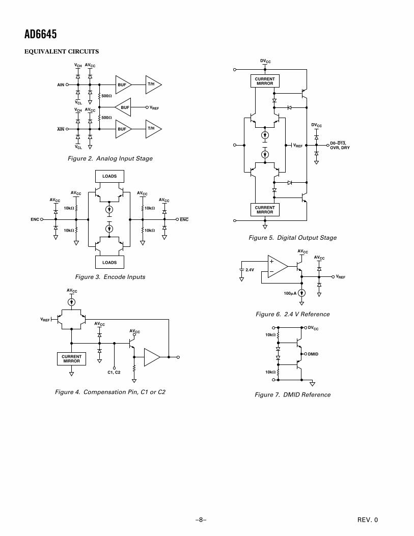
EQUIVALENT CIRCUITS
BUF T/H
BUF
BUF T/H
VCH AVCC
500�
VCL
AIN
VCH AVCC
VCL
AIN
500�
VREF
Figure 2. Analog Input Stage
LOADS
LOADS
10k�
10k�
10k�
10k�
ENCENC
AVCC
AVCC
AVCC
AVCC
Figure 3. Encode Inputs
AVCC
CURRENTMIRROR
VREF
AVCC
AVCC
C1, C2
Figure 4. Compensation Pin, C1 or C2
CURRENTMIRROR
CURRENTMIRROR
VREFD0�D13,OVR, DRY
DVCC
DVCC
Figure 5. Digital Output Stage
AVCC
AVCC
VREF
100�A
2.4V
Figure 6. 2.4 V Reference
10k�
DMID
10k�
DVCC
Figure 7. DMID Reference
REV. 0 –9–
AD6645
FREQUENCY � MHz
�1300 5 10 15 20 25 30 35 40
�120
�110
�100
�90
�80
�70
�60
�50
�40
�30
�20
�10
0ENCODE = 80MSPSAIN = 2.2MHz @ �1dBFSSNR = 75.0dBSFDR = 93.0dBc
dB
FS
2
65
4
3
TPC 1. Single Tone @ 2.2 MHz
FREQUENCY � MHz
�1300 5 10 15 20 25 30 35 40
�120
�110
�100
�90
�80
�70
�60
�50
�40
�30
�20
�10
0
dB
FS
26
5
4
3
ENCODE = 80MSPSAIN = 15.5MHz @ �1dBFSSNR = 75.0dBSFDR = 93.0dBc
TPC 2. Single Tone @ 15.5 MHz
FREQUENCY � MHz
�1300 5 10 15 20 25 30 35 40
�120
�110
�100
�90
�80
�70
�60
�50
�40
�30
�20
�10
0ENCODE = 80MSPSAIN = 29.5MHz @ �1dBFSSNR = 74.5dBSFDR = 93.0dBc
dB
FS
2
6
5
4
3
TPC 3. Single Tone @ 29.5 MHz
Typical Performance Characteristics–
FREQUENCY � MHz
�1300 5 10 15 20 25 30 35 40
�120
�110
�100
�90
�80
�70
�60
�50
�40
�30
�20
�10
0ENCODE = 80MSPSAIN = 69.1MHz @ �1dBFSSNR = 73.5dBSFDR = 89.0dBc
dB
FS
2
6 54
3
TPC 4. Single Tone @ 69.1 MHz
FREQUENCY � MHz
�1300 5 10 15 20 25 30 35 40
�120
�110
�100
�90
�80
�70
�60
�50
�40
�30
�20
�10
0
dB
FS
2
6
54
3
ENCODE = 80MSPSAIN = 150MHz @ �1dBFSSNR = 73.0dBSFDR = 70.0dBc
TPC 5. Single Tone @ 150 MHz
FREQUENCY � MHz
�1300 5 10 15 20 25 30 35 40
�120
�110
�100
�90
�80
�70
�60
�50
�40
�30
�20
�10
0
dB
FS
2
6 54
3
ENCODE = 80MSPSAIN = 200MHz @ �1dBFSSNR = 72.0dBSFDR = 64.0dBc
TPC 6. Single Tone @ 200 MHz

REV. 0
AD6645
–10–
FREQUENCY � MHz
SN
R �
dB
0 10 20 30 40 50 60 70
ENCODE = 80MSPS @ AIN = �1dBFSTEMP = �40 C, +25 C, +85 C
72.0
72.5
73.0
73.5
74.0
74.5
75.0
75.5
T = +25 C
T = +85 C
T = �40 C
TPC 7. Noise vs. Analog Frequency
ANALOG INPUT FREQUENCY � MHz
WO
RS
T C
AS
E H
AR
MO
NIC
� d
Bc
0 10 20 30 40 50 60 70
ENCODE = 80MSPS @ AIN = �1dBFSTEMP = �40 C, +25 C, +85 C
80
82
84
86
88
90
92
94
T = +25 C
T = �40 C, +85 C
TPC 8. Harmonics vs. Analog Frequency
ANALOG FREQUENCY � MHz
SN
R �
dB
0 20 8040 10060
ENCODE = 80MSPS @ AIN = �1dBFSTEMP = 25 C
70
71
72
73
74
75
76
120 140 160 180 200
TPC 9. Noise vs. Analog Frequency (IF)
ANALOG FREQUENCY � MHz
HA
RM
ON
ICS
� d
Bc
0 20 8040 10060
ENCODE = 80MSPS @ AIN = �1dBFSTEMP = 25 C
60
65
120 140 160 180 200
70
80
90
100
75
85
95
WORST OTHER SPUR
HARMONICS (2ND, 3RD)
TPC 10. Harmonics vs. Analog Frequency (IF)
ANALOG INPUT POWER LEVEL � dBFS
WO
RS
T C
AS
E S
PU
RIO
US
� d
BF
S A
ND
dB
c
0�90
10
20
30
40
50
60
70
80
90
100
110
�80 �70 �60 �50 �40 �30 �20
ENCODE = 80MSPSAIN = 30.5MHz
dBc
SFDR = 90dBREFERENCE LINE
120
dBFS
�10 0
TPC 11. Single Tone SFDR @ 30.5 MHz
ANALOG INPUT POWER LEVEL � dBFS
WO
RS
T C
AS
E S
PU
RIO
US
� d
BF
S A
ND
dB
c
0�90
10
20
30
40
50
60
70
80
90
100
110
�80 �70 �60 �50 �40 �30 �20
ENCODE = 80MSPSAIN = 69.1MHz
dBc
SFDR = 90dBREFERENCE LINE
120
dBFS
�10 0
TPC 12. Single Tone SFDR @ 69.1 MHz
REV. 0 –11–
AD6645ENCODE = 80MSPSAIN = 30.5MHz,31.5MHz (�7dBFS)NO DITHER
FREQUENCY � MHz
�1300 5 10 15 20 25 30 35 40
�120
�110
�100
�90
�80
�70
�60
�50
�40
�30
�20
�10
0d
BF
S
2F1+F2
F1+F2
F2�F1
2F2+F1
2F1�F2
2F2�F1
TPC 13. Two Tones @ 30.5 MHz and 31.5 MHz
INPUT POWER LEVEL � F1 = F2 dBFS
WO
RS
T C
AS
E S
PU
RIO
US
� d
BF
S A
ND
dB
c
0�77
10
20
30
40
50
60
70
80
90
100
110
�67 �57 �47 �37 �27 �17 �7
ENCODE = 80MSPSF1 = 30.5MHzF2 = 31.5MHz
dBc
dBFS
SFDR = 90dBREFERENCE LINE
TPC 14. Two Tone SFDR @ 30.5 MHz and 31.5 MHz
ENCODE FREQUENCY � MHz
SN
R, W
OR
ST
CA
SE
SP
UR
IOU
S �
dB
AN
D d
Bc
1565
70
80
90
30 45 60 75 90 105
WORST SPUR @ AIN = 2.2MHz
SNR @ AIN = 2.2MHz75
85
95
100
TPC 15. SNR, Worst Spurious vs. Encode @ 2.2 MHz
2F2�F1
ENCODE = 80MSPSAIN = 55.25MHz,56.25MHz (�7dBFS)NO DITHER
FREQUENCY � MHz
�1300 5 10 15 20 25 30 35 40
�120
�110
�100
�90
�80
�70
�60
�50
�40
�30
�20
�10
0
dB
FS 2
F1+F2
F1+F2
F2�F1
2F2+F1
2F1�F2
TPC 16. Two Tone SFDR @ 55.25 MHz and 56.25 MHz
�77 �67 �57 �47 �37 �27 �17 �7INPUT POWER LEVEL � F1 = F2 dBFS
WO
RS
T C
AS
E S
PU
RIO
US
� d
BF
S A
ND
dB
c
0
10
20
30
40
50
60
70
80
90
100
110
ENCODE = 80MSPSF1 = 55.25MHzF2 = 56.25MHz
dBc
dBFS
SFDR = 90dBREFERENCE LINE
TPC 17. Two Tone SFDR @ 55.25 MHz and 56.25 MHz
ENCODE FREQUENCY � MHz
SN
R, W
OR
ST
CA
SE
SP
UR
IOU
S �
dB
AN
D d
Bc
1565
70
80
90
30 45 60 75 90 105
WORST SPUR @ AIN = 69.1MHz
SNR @ AIN = 69.1MHz75
85
95
TPC 18. SNR, Worst Spurious vs. Encode @ 69.1 MHz

REV. 0
AD6645
–12–
FREQUENCY � MHz0
�130
�120
�110
�100
�90
�80
�70
�60
�50
�40
�30
�20
�10
0
5 10 15 20 25 30 35 40
53
2
64
dB
FS
ENCODE = 80.0MSPSAIN = 30.5MHz @ �29.5 dBFSNO DITHER
TPC 19. 1 M FFT without Dither
ANALOG INPUT LEVEL
900
10
20
30
40
50
60
70
80
90
100
110
80 70 60 50 40 30 20 10 0dBFS
ENCODE = 80.0MSPSAIN = 30.5MHzNO DITHER
SFDR = 90 dBREFERENCE LINEW
OR
ST
-CA
SE
SP
UR
IOU
S d
Bc
TPC 20. SFDR without Dither
FREQUENCY � MHz
�1300 5 10 15 20 25 30 35 40
�120
�110
�100
�90
�80
�70
�60
�50
�40
�30
�20
�10
0
dB
FS
26
5
4
3
ENCODE = 76.8MSPSAIN = 69.1MHz @�1dBFSSNR = 73.5dBSFDR = 89.0dBc
TPC 21. Single Tone 69.1 MHz: Encode = 76.8 MSPS
FREQUENCY � MHz
�1300 5 10 15 20 25 30 35 40
�120
�110
�100
�90
�80
�70
�60
�50
�40
�30
�20
�10
0
5 3
2
6
4
dB
FS
ENCODE = 80.0MSPSAIN = 30.5MHz @ �29.5dBFSWITH DITHER @ �19.2 dBm
TPC 22. 1 M FFT with Dither
ANALOG INPUT LEVEL
�900
10
20
30
40
50
60
70
80
90
100
110
�80 �70 �60 �50 �40 �30 �20 �10 0dBFS
ENCODE = 80.0MSPSAIN = 30.5MHzWITH DITHER @ �19.2 dBm
SFDR = 90 dBREFERENCE LINE
SFDR = 100 dBREFERENCE LINE
WO
RS
T-C
AS
E S
PU
RIO
US
dB
c
TPC 23. SFDR with Dither
FREQUENCY � MHz
�1300 5 10 15 20 25 30 35 40
�120
�110
�100
�90
�80
�70
�60
�50
�40
�30
�20
�10
0
dB
FS
2 6 543
ENCODE = 76.8MSPSAIN = WCDMA @ 69.1MHz
TPC 24. WCDMA Tone 69.1 MHz: Encode = 76.8 MSPS

REV. 0 –13–
AD6645
FREQUENCY � MHz
�1300 5 10 15 20 25 30 35 40
�120
�110
�100
�90
�80
�70
�60
�50
�40
�30
�20
�10
0d
BF
SENCODE = 76.8MSPSAIN = 2WCDMA @ 59.6MHz
TPC 25. 2 WCDMA Carriers @ AIN = 59.6 MHz:Encode = 76.8 MSPS
FREQUENCY � MHz0 2.5 5.0 7.5 10.0 12.5 15.0 17.5 20.0 22.5 25.0 27.5 30.0
�130
�120
�110
�100
�90
�80
�70
�60
�50
�40
�30
�20
�10
0ENCODE = 61.44MSPSAIN = 4WCDMA @ 46.08MHz
dB
FS
TPC 26. 4 WCDMA Carriers @ AIN = 46.08 MHz:Encode = 61.44 MSPS
6 5 4 2 3
FREQUENCY � MHz
�1300
�120
�110
�100
�90
�80
�70
�60
�50
�40
�30
�20
�10
0
5 10 15 20 25 30 35 40
ENCODE = 76.8MSPSAIN = WCDMA @ 140MHz
dB
FS
TPC 27. WCDMA Tone 140 MHz: Encode = 76.8 MSPS
�130
�120
�110
�100
�90
�80
�70
�60
�50
�40
�30
�20
�10
0
2 3 6 4 5
ENCODE = 61.44MSPSAIN = WCDMA @ 190MHz
dB
FS
FREQUENCY � MHz0 2.5 5.0 7.5 10.0 12.5 15.0 17.5 20.0 22.5 25.0 27.5 30.0
TPC 28. WCDMA Tone 190 MHz: Encode = 61.44 MSPS
REV. 0
AD6645
–14–
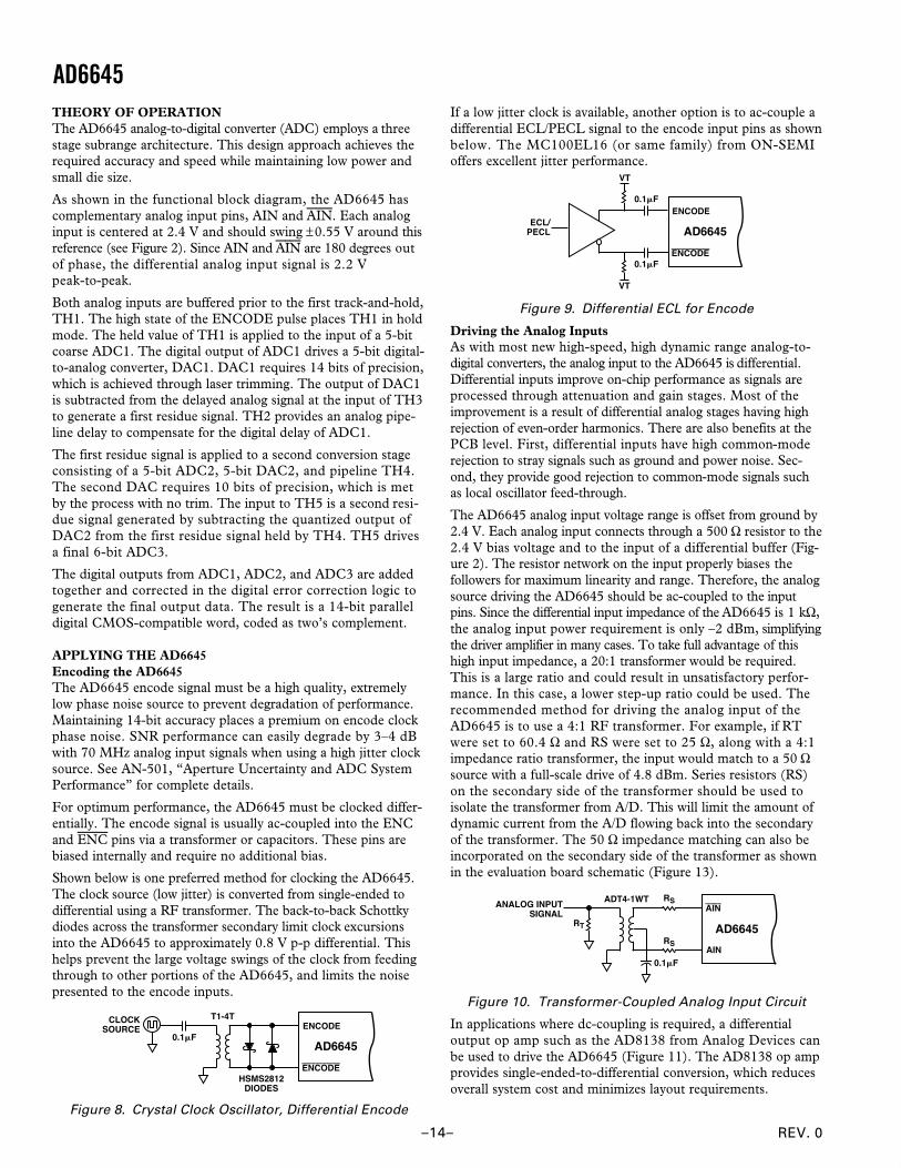
THEORY OF OPERATIONThe AD6645 analog-to-digital converter (ADC) employs a threestage subrange architecture. This design approach achieves therequired accuracy and speed while maintaining low power andsmall die size.
As shown in the functional block diagram, the AD6645 hascomplementary analog input pins, AIN and AIN. Each analoginput is centered at 2.4 V and should swing ± 0.55 V around thisreference (see Figure 2). Since AIN and AIN are 180 degrees outof phase, the differential analog input signal is 2.2 Vpeak-to-peak.
Both analog inputs are buffered prior to the first track-and-hold,TH1. The high state of the ENCODE pulse places TH1 in holdmode. The held value of TH1 is applied to the input of a 5-bitcoarse ADC1. The digital output of ADC1 drives a 5-bit digital-to-analog converter, DAC1. DAC1 requires 14 bits of precision,which is achieved through laser trimming. The output of DAC1is subtracted from the delayed analog signal at the input of TH3to generate a first residue signal. TH2 provides an analog pipe-line delay to compensate for the digital delay of ADC1.
The first residue signal is applied to a second conversion stageconsisting of a 5-bit ADC2, 5-bit DAC2, and pipeline TH4.The second DAC requires 10 bits of precision, which is metby the process with no trim. The input to TH5 is a second resi-due signal generated by subtracting the quantized output ofDAC2 from the first residue signal held by TH4. TH5 drivesa final 6-bit ADC3.
The digital outputs from ADC1, ADC2, and ADC3 are addedtogether and corrected in the digital error correction logic togenerate the final output data. The result is a 14-bit paralleldigital CMOS-compatible word, coded as two’s complement.
APPLYING THE AD6645Encoding the AD6645The AD6645 encode signal must be a high quality, extremelylow phase noise source to prevent degradation of performance.Maintaining 14-bit accuracy places a premium on encode clockphase noise. SNR performance can easily degrade by 3–4 dBwith 70 MHz analog input signals when using a high jitter clocksource. See AN-501, “Aperture Uncertainty and ADC SystemPerformance” for complete details.
For optimum performance, the AD6645 must be clocked differ-entially. The encode signal is usually ac-coupled into the ENCand ENC pins via a transformer or capacitors. These pins arebiased internally and require no additional bias.
Shown below is one preferred method for clocking the AD6645.The clock source (low jitter) is converted from single-ended todifferential using a RF transformer. The back-to-back Schottkydiodes across the transformer secondary limit clock excursionsinto the AD6645 to approximately 0.8 V p-p differential. Thishelps prevent the large voltage swings of the clock from feedingthrough to other portions of the AD6645, and limits the noisepresented to the encode inputs.
ENCODE
ENCODE
0.1�F
T1-4T
HSMS2812DIODES
AD6645
CLOCKSOURCE
Figure 8. Crystal Clock Oscillator, Differential Encode
If a low jitter clock is available, another option is to ac-couple adifferential ECL/PECL signal to the encode input pins as shownbelow. The MC100EL16 (or same family) from ON-SEMIoffers excellent jitter performance.
ENCODE
ENCODE
AD6645
VT
VT
0.1�F
0.1�F
ECL/PECL
Figure 9. Differential ECL for Encode
Driving the Analog InputsAs with most new high-speed, high dynamic range analog-to-digital converters, the analog input to the AD6645 is differential.Differential inputs improve on-chip performance as signals areprocessed through attenuation and gain stages. Most of theimprovement is a result of differential analog stages having highrejection of even-order harmonics. There are also benefits at thePCB level. First, differential inputs have high common-moderejection to stray signals such as ground and power noise. Sec-ond, they provide good rejection to common-mode signals suchas local oscillator feed-through.
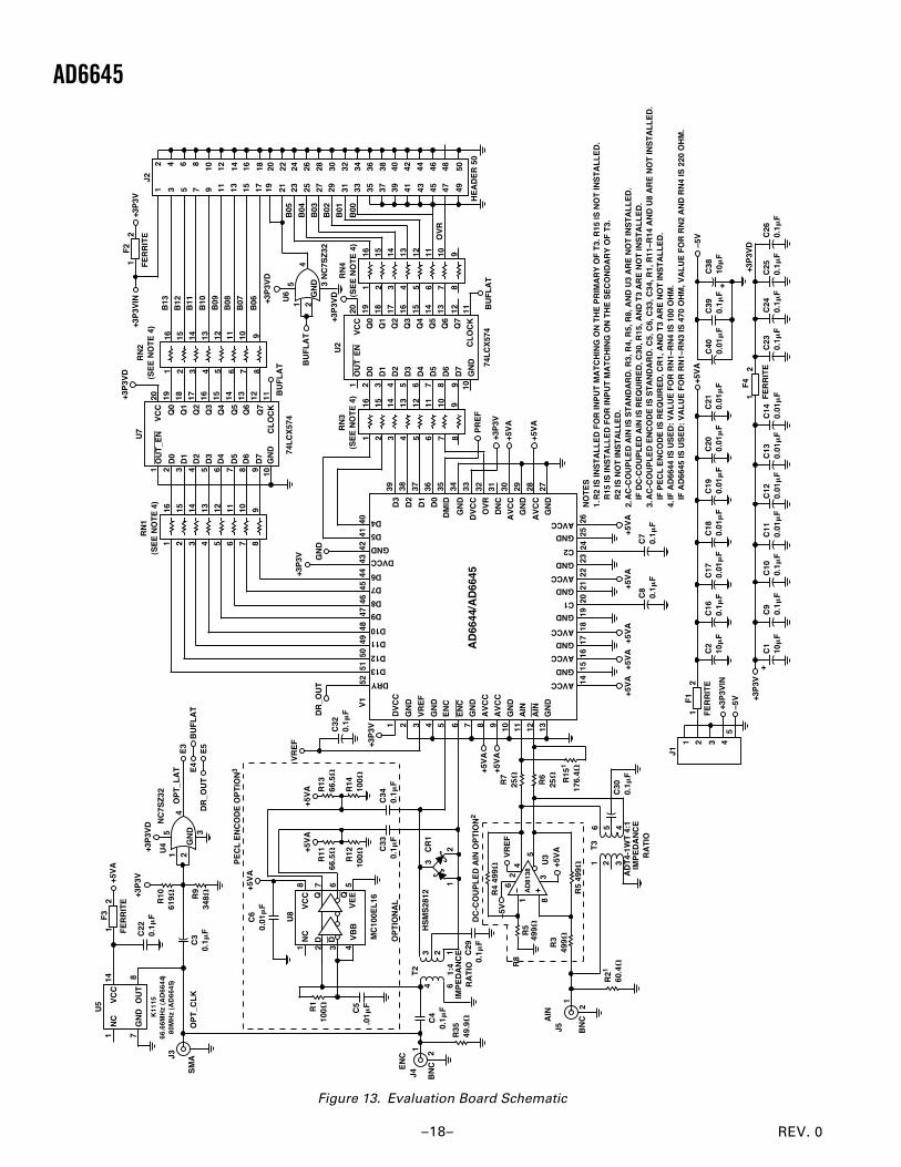
The AD6645 analog input voltage range is offset from ground by2.4 V. Each analog input connects through a 500 W resistor to the2.4 V bias voltage and to the input of a differential buffer (Fig-ure 2). The resistor network on the input properly biases thefollowers for maximum linearity and range. Therefore, the analogsource driving the AD6645 should be ac-coupled to the inputpins. Since the differential input impedance of the AD6645 is 1 kW,the analog input power requirement is only –2 dBm, simplifyingthe driver amplifier in many cases. To take full advantage of thishigh input impedance, a 20:1 transformer would be required.This is a large ratio and could result in unsatisfactory perfor-mance. In this case, a lower step-up ratio could be used. Therecommended method for driving the analog input of theAD6645 is to use a 4:1 RF transformer. For example, if RTwere set to 60.4 W and RS were set to 25 W, along with a 4:1impedance ratio transformer, the input would match to a 50 Wsource with a full-scale drive of 4.8 dBm. Series resistors (RS)on the secondary side of the transformer should be used toisolate the transformer from A/D. This will limit the amount ofdynamic current from the A/D flowing back into the secondaryof the transformer. The 50 W impedance matching can also beincorporated on the secondary side of the transformer as shownin the evaluation board schematic (Figure 13).
AIN
AINADT4-1WT
AD6645
ANALOG INPUTSIGNAL
0.1�F
RT
RS
RS
Figure 10. Transformer-Coupled Analog Input Circuit
In applications where dc-coupling is required, a differentialoutput op amp such as the AD8138 from Analog Devices canbe used to drive the AD6645 (Figure 11). The AD8138 op ampprovides single-ended-to-differential conversion, which reducesoverall system cost and minimizes layout requirements.

REV. 0 –15–
AD6645
AD6645AIN
AIN
VREF
AD8138VOCM
5V
499�
499�
499�
499�
25�
25�
CF
VIN
CF
DIGITALOUTPUTS
Figure 11. DC-Coupled Analog Input Circuit
Power SuppliesCare should be taken when selecting a power source. The use oflinear dc supplies with rise-times of <45 ms is highly recom-mended. Switching supplies tend to have radiated componentsthat may be “received” by the AD6645. Each of the powersupply pins should be decoupled as closely to the package aspossible using 0.1 mF chip capacitors.
The AD6645 has separate digital and analog power supply pins.The analog supplies are denoted AVCC and the digital supplypins are denoted DVCC. Although analog and digital suppliesmay be tied together, best performance is achieved when thesupplies are separate. This is because the fast digital outputswings can couple switching current back into the analog supplies.Note that AVCC must be held within 5% of 5 V. The AD6645 isspecified for DVCC = 3.3 V as this is a common supply fordigital ASICS.
Digital OutputsCare must be taken when designing the data receivers for the AD6645.It is recommended that the digital outputs drive a series resistorfollowed by a gate such as the 74LCX574. To minimize capaci-tive loading, there should only be one gate on each output pin.An example of this is shown in the evaluation board schematicshown in Figure 13. The digital outputs of the AD6645 have aconstant output slew rate of 1 V/ns. A typical CMOS gate combinedwith a PCB trace will have a load of approximately 10 pF. There-fore, as each bit switches 10 mA 10 1 1pF V ns¥ ∏( ) ofdynamic current per bit will flow in or out of the device. A full-scale transition can cause up to 140 mA (14 bits ¥ 10 mA/bit) ofcurrent to flow through the output stages. The series resistorsshould be placed as close to the AD6645 as possible to limit theamount of current that can flow into the output stage. Theseswitching currents are confined between ground and the DVCCpin. Standard TTL gates should be avoided since they can appre-ciably add to the dynamic switching currents of the AD6645. Itshould be noted that extra capacitive loading will increase out-put timing and invalidate timing specifications. Digital outputtiming is guaranteed for output loads up to 10 pF.
Digital output states for given analog input levels are shown in Table I.
GroundingFor optimum performance, it is highly recommended that a com-mon ground be utilized between the analog and digital powerplanes. The primary concern with splitting grounds is that dynamiccurrents may be forced to travel significant distances in the sys-tem before recombining back at the common source ground. Thiscan result in a large and undesirable ground loop. The mostcommon place for this to occur is on the digital outputs of theADC. Ground loops can contribute to digital noise being coupledback onto the ADC front end. This can manifest itself as eitherharmonic spurs, or very high order spurious products that cancause excessive spikes on the noise floor. This noise coupling isless likely to occur at lower clock speeds since the digital noise hasmore time to settle between samples. In general, splitting theanalog and digital grounds can frequently contribute to undesir-able EMI-RFI and should therefore be avoided.
Conversely, if not properly implemented, common grounding canactually impose additional noise issues since the digital groundcurrents are riding on top of the analog ground currents in closeproximity to the ADC input. To minimize the potential fornoise coupling further, it is highly recommended that multipleground return traces/vias be placed such that the digital outputcurrents do not flow back towards the analog front end, but arerouted quickly away from the ADC. This does not require asplit in the ground plane and can be accomplished by simplyplacing substantial ground connections directly back to thesupply at a point between the analog front end and the digitaloutputs. The judicious use of ceramic chip capacitors betweenthe power supply and ground planes will also help suppressdigital noise. The layout should incorporate enough bulk capacitanceto supply the peak current requirements during switching periods.
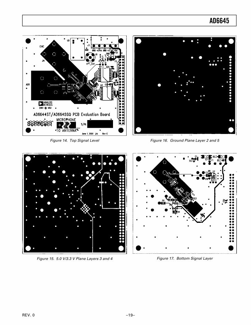
Layout InformationThe schematic of the evaluation board (Figure 13) represents atypical implementation of the AD6645. A multilayer board isrecommended to achieve best results. It is highly recommendedthat high quality, ceramic chip capacitors be used to decoupleeach supply pin to ground directly at the device. The pinout ofthe AD6645 facilitates ease of use in the implementation ofhigh-frequency, high-resolution design practices. All of the digitaloutputs are segregated to two sides of the chip, with the inputs onthe opposite side for isolation purposes.
Care should be taken when routing the digital output traces. Toprevent coupling through the digital outputs into the analogportion of the AD6645, minimal capacitive loading should beplaced on these outputs. It is recommended that a fan-out ofonly one gate should be used for all AD6645 digital outputs.
The layout of the encode circuit is equally critical. Any noisereceived on this circuitry will result in corruption in the digitiza-tion process and lower overall performance. The encode clockmust be isolated from the digital outputs and the analog inputs.
Table I. Two’s Complement Output Coding
AIN AIN Output OutputLevel Level State Code
VREF + 0.55 V VREF – 0.55 V Positive FS 01 1111 1111 1111VREF VREF Midscale 00…0/11…1VREF – 0.55 V VREF + 0.55 V Negative FS 10 0000 0000 0000

REV. 0
AD6645
–16–
Jitter ConsiderationsThe signal-to-noise ratio (SNR) for an ADC can be predicted.When normalized to ADC codes, the above equation accuratelypredicts the SNR based on three terms. These are jitter, averageDNL error, and thermal noise. Each of these terms contributesto the noise within the converter.
FANALOG = analog input frequencytj rms = rms jitter of the encode (rms sum of encode source andinternal encode circuitry)� = average DNL of the ADC (typically 0.41 LSB)n = number of bits in the ADCVNOISE rms = V rms thermal noise referred to the analog input ofthe ADC (typically 0.9 LSB rms)
For a 14-bit analog-to-digital converter, like the AD6645, aperturejitter can greatly affect the SNR performance as the analogfrequency is increased. The chart below shows a family of curvesthat demonstrate the expected SNR performance of the AD6645 asjitter increases. The chart is derived from the above equation.
For a complete discussion of aperture jitter, please consultAN-501, “Aperture Uncertainty and ADC System Performance.”
JITTER � ps
550 0.1
SN
R �
dB
FS
60
65
70
75
80
0.2 0.3 0.4 0.5 0.6
AIN = 110MHz
AIN = 150MHz
AIN = 190MHz
AIN = 30MHz
AIN = 70MHz
Figure 12. Jitter vs. SNR
SNR F tV
j rms nN
n= - ¥ ¥( ) ++Ê
ËÁ��̄ +
¥ ¥ÊËÁ
��̄
È
ÎÍÍ
ù
ûúú
1 76 20 212
2 22
22 2
1
2
. log p eANALOG
OISE rms
REV. 0 –17–
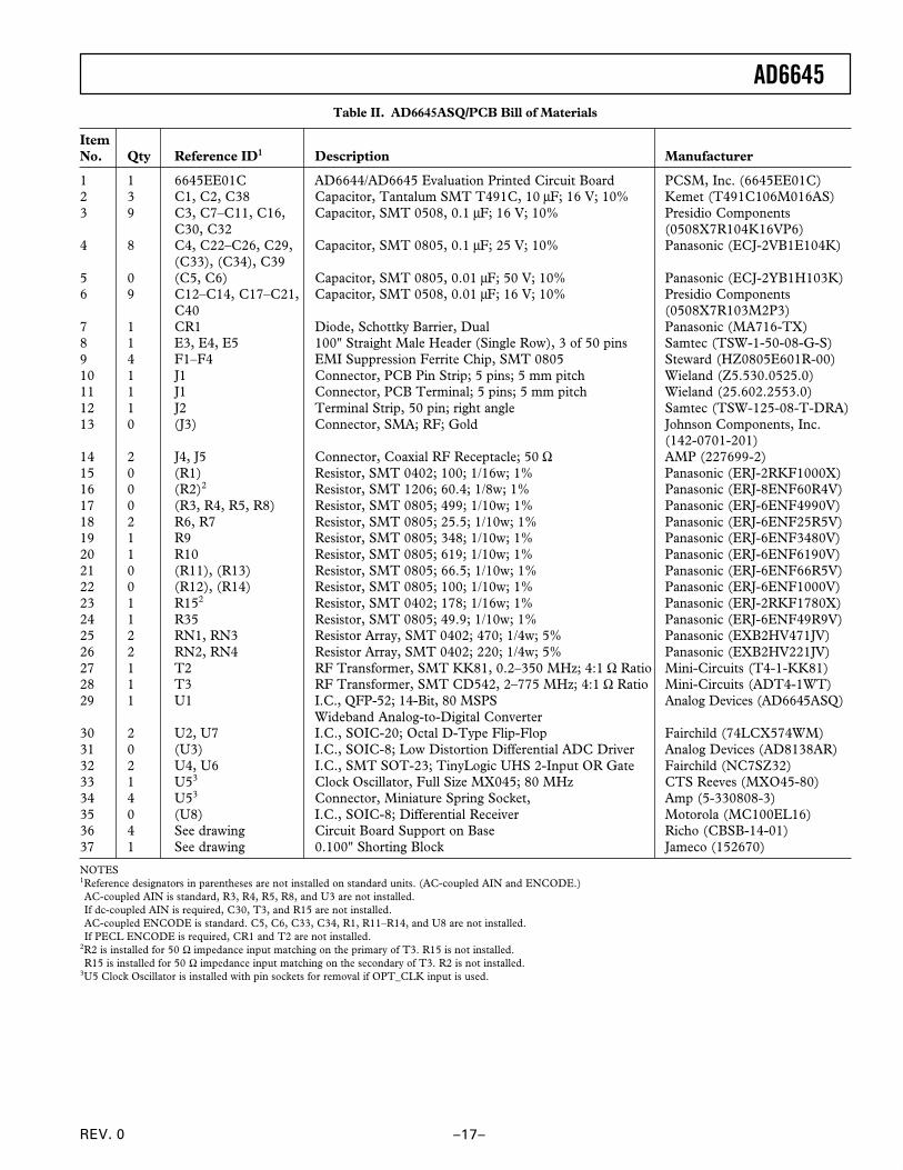
AD6645Table II. AD6645ASQ/PCB Bill of Materials
ItemNo. Qty Reference ID1 Description Manufacturer
1 1 6645EE01C AD6644/AD6645 Evaluation Printed Circuit Board PCSM, Inc. (6645EE01C)2 3 C1, C2, C38 Capacitor, Tantalum SMT T491C, 10 mF; 16 V; 10% Kemet (T491C106M016AS)3 9 C3, C7–C11, C16, Capacitor, SMT 0508, 0.1 mF; 16 V; 10% Presidio Components
C30, C32 (0508X7R104K16VP6)4 8 C4, C22–C26, C29, Capacitor, SMT 0805, 0.1 mF; 25 V; 10% Panasonic (ECJ-2VB1E104K)
(C33), (C34), C395 0 (C5, C6) Capacitor, SMT 0805, 0.01 mF; 50 V; 10% Panasonic (ECJ-2YB1H103K)6 9 C12–C14, C17–C21, Capacitor, SMT 0508, 0.01 mF; 16 V; 10% Presidio Components
C40 (0508X7R103M2P3)7 1 CR1 Diode, Schottky Barrier, Dual Panasonic (MA716-TX)8 1 E3, E4, E5 100" Straight Male Header (Single Row), 3 of 50 pins Samtec (TSW-1-50-08-G-S)9 4 F1–F4 EMI Suppression Ferrite Chip, SMT 0805 Steward (HZ0805E601R-00)10 1 J1 Connector, PCB Pin Strip; 5 pins; 5 mm pitch Wieland (Z5.530.0525.0)11 1 J1 Connector, PCB Terminal; 5 pins; 5 mm pitch Wieland (25.602.2553.0)12 1 J2 Terminal Strip, 50 pin; right angle Samtec (TSW-125-08-T-DRA)13 0 (J3) Connector, SMA; RF; Gold Johnson Components, Inc.
(142-0701-201)14 2 J4, J5 Connector, Coaxial RF Receptacle; 50 W AMP (227699-2)15 0 (R1) Resistor, SMT 0402; 100; 1/16w; 1% Panasonic (ERJ-2RKF1000X)16 0 (R2)2 Resistor, SMT 1206; 60.4; 1/8w; 1% Panasonic (ERJ-8ENF60R4V)17 0 (R3, R4, R5, R8) Resistor, SMT 0805; 499; 1/10w; 1% Panasonic (ERJ-6ENF4990V)18 2 R6, R7 Resistor, SMT 0805; 25.5; 1/10w; 1% Panasonic (ERJ-6ENF25R5V)19 1 R9 Resistor, SMT 0805; 348; 1/10w; 1% Panasonic (ERJ-6ENF3480V)20 1 R10 Resistor, SMT 0805; 619; 1/10w; 1% Panasonic (ERJ-6ENF6190V)21 0 (R11), (R13) Resistor, SMT 0805; 66.5; 1/10w; 1% Panasonic (ERJ-6ENF66R5V)22 0 (R12), (R14) Resistor, SMT 0805; 100; 1/10w; 1% Panasonic (ERJ-6ENF1000V)23 1 R152 Resistor, SMT 0402; 178; 1/16w; 1% Panasonic (ERJ-2RKF1780X)24 1 R35 Resistor, SMT 0805; 49.9; 1/10w; 1% Panasonic (ERJ-6ENF49R9V)25 2 RN1, RN3 Resistor Array, SMT 0402; 470; 1/4w; 5% Panasonic (EXB2HV471JV)26 2 RN2, RN4 Resistor Array, SMT 0402; 220; 1/4w; 5% Panasonic (EXB2HV221JV)27 1 T2 RF Transformer, SMT KK81, 0.2–350 MHz; 4:1 W Ratio Mini-Circuits (T4-1-KK81)28 1 T3 RF Transformer, SMT CD542, 2–775 MHz; 4:1 W Ratio Mini-Circuits (ADT4-1WT)29 1 U1 I.C., QFP-52; 14-Bit, 80 MSPS Analog Devices (AD6645ASQ)
Wideband Analog-to-Digital Converter30 2 U2, U7 I.C., SOIC-20; Octal D-Type Flip-Flop Fairchild (74LCX574WM)31 0 (U3) I.C., SOIC-8; Low Distortion Differential ADC Driver Analog Devices (AD8138AR)32 2 U4, U6 I.C., SMT SOT-23; TinyLogic UHS 2-Input OR Gate Fairchild (NC7SZ32)33 1 U53 Clock Oscillator, Full Size MX045; 80 MHz CTS Reeves (MXO45-80)34 4 U53 Connector, Miniature Spring Socket, Amp (5-330808-3)35 0 (U8) I.C., SOIC-8; Differential Receiver Motorola (MC100EL16)36 4 See drawing Circuit Board Support on Base Richo (CBSB-14-01)37 1 See drawing 0.100" Shorting Block Jameco (152670)
NOTES1Reference designators in parentheses are not installed on standard units. (AC-coupled AIN and ENCODE.)AC-coupled AIN is standard, R3, R4, R5, R8, and U3 are not installed.If dc-coupled AIN is required, C30, T3, and R15 are not installed.AC-coupled ENCODE is standard. C5, C6, C33, C34, R1, R11–R14, and U8 are not installed.If PECL ENCODE is required, CR1 and T2 are not installed.
2R2 is installed for 50 W impedance input matching on the primary of T3. R15 is not installed.R15 is installed for 50 W impedance input matching on the secondary of T3. R2 is not installed.
3U5 Clock Oscillator is installed with pin sockets for removal if OPT_CLK input is used.
REV. 0
AD6645
–18–
1 2
3
45
1 2 3 4 5 6 7 8 9 10 11 13
1415
1617
1819
2021
2223
2425
26
27282930313233343536373839
40
12
4142
4344
4546
4748
4950
5152
1 2 3 4 5 6 7 8910111213141516
RN
3(S
EE
NO
TE
4)
1 2 3 4 5 6 7 8910111213141516
1 2 3 4 5 6 7 8 9 1011121314151617181920
U2
GN
DC
LO
CK
OU
T E
N
D0
D1
D2
D3
D4
D5
D6
D7
VC
C
Q0
Q1
Q2
Q3
Q4
Q5
Q6
Q7
1 2 3 4 5 6 7 8 9 1011121314151617181920
U7
GN
DC
LO
CK
OU
T_E
N
D0
D1
D2
D3
D4
D5
D6
D7
VC
C
Q0
Q1
Q2
Q3
Q4
Q5
Q6
Q7
1 2 3 4 5 6 7 8910111213141516
RN
1(S
EE
NO
TE
4)
1 2 3 4 5 6 7 8910111213141516
12
34
5 7 9 11 13 15 17 19 21 23 25 27 29 31 33 35 37 39 41 43 45 47 49
6 8
10 12 14 16 18 20 22 24 26 28 30 32 34 36 38 40 42 44 46 48 50
R2
IS IN
ST
AL
LE
D F
OR
INP
UT
MA
TC
HIN
G O
N T
HE
PR
IMA
RY
OF
T3.
R15
IS N
OT
INS
TA
LL
ED
.R
15 IS
INS
TA
LL
ED
FO
R IN
PU
T M
AT
CH
ING
ON
TH
E S
EC
ON
DA
RY
OF
T3.
R2
IS N
OT
INS
TA
LL
ED
.A
C-C
OU
PL
ED
AIN
IS S
TA
ND
AR
D. R
3, R
4, R
5, R
8, A
ND
U3
AR
E N
OT
INS
TA
LL
ED
.IF
DC
-CO
UP
LE
D A
IN IS
RE
QU
IRE
D, C
30, R
15, A
ND
T3
AR
E N
OT
INS
TA
LL
ED
.A
C-C
OU
PL
ED
EN
CO
DE
IS S
TA
ND
AR
D. C
5, C
6, C
33, C
34, R
1, R
11�R
14 A
ND
U8
AR
E N
OT
INS
TA
LL
ED
.IF
PE
CL
EN
CO
DE
IS R
EQ
UIR
ED
, CR
1, A
ND
T3
AR
E N
OT
INS
TA
LL
ED
.IF
AD
6644
IS U
SE
D:
VA
LU
E F
OR
RN
1�R
N4
IS 1
00 O
HM
.IF
AD
6645
IS U
SE
D:
VA
LU
E F
OR
RN
1�R
N3
IS 4
70 O
HM
, VA
LU
E F
OR
RN
2 A
ND
RN
4 IS
220
OH
M.
NO
TE
S1. 2. 3. 4.
AD
6644
/AD
6645
GN
D
VR
EF
GN
DE
NC
EN
C
GN
D
AV
CC
AV
CC
GN
D
AIN
AIN
GN
D
DV
CC
AVCC
GND
GND
GND
C1
C2
AVCC
AVCC
GND
AVCC
GND
GND
AVCC
D3
D2
D1
D0
DM
ID
GN
D
DV
CC
OV
R
AV
CC
DN
C
GN
D
AV
CC
GN
D
DRY
D13
D12
D11
D10
D9
D8
D7
D6
DVCC
GND
D5
D4
DC
-CO
UP
LE
D A
IN O
PT
ION
2
12
1 2
3
4
5
GN
DB
UF
LA
T
U6
BU
FL
AT
FE
RR
ITE
12
F2
+3P
3VIN
+3P
3VJ2
+3P
3VD
1 2 3 4
12
J1
+3P
3VIN
�5V
5
F1
C2
10�
FC
160.
1�F
C17
0.01
�F
C18
0.01
�F
C19
0.01
�F
C20
0.01
�F
C21
0.01
�F
C40
0.01
�F
C39
0.1�
FC
3810
�F
12
+3P
3VC
110
�F
C9
0.1�
FC
100.
1�F
C11
0.01
�F
C12
0.01
�F
C13
0.01
�F
C14
0.01
�F
C23
0.1�
FC
240.
1�F
C25
0.1�
FC
260.
1�F
+5V
A+5
VA
+5V
A+5
VA
+5V
A
C8
0.1�
FC
70.
1�F
+5V
A
+5V
A
+3P
3V
PR
EF
GN
D
+3P
3V
DR
_OU
T
+3P
3VC32
0.1�
F
VR
EF
+5V
A
+5V
A
RN
4(S
EE
NO
TE
4)
R7
25�
R6
25� R15
1
176.
4�
1 2 3
6 5 4
T3
IMP
ED
AN
CE
RA
TIO
AD
T4-
1WT
4:1
C30
0.1�
F
R21
60.4
�
1
2
J5A
IN
1 832
64
5A
D81
38
R4
499�
VR
EF
�5V
U3
+5V
A
R5
499�
R3
499�
R5
499�
C29
0.1�
F
T2
IMP
ED
AN
CE
RA
TIO
1:4
3 2 1
4 61
2
3C
R1
C4
0.1�
F
1 2
EN
CJ4
R35
49.9
�
R13
66.5
�
R14
100�
C34
0.1�
FC
330.
1�F
R11
66.5
�
R12
100�
+5V
A+5
VA
1 2 3 4
8 7 6 5
NC VB
B
VC
C
VE
E
U8
+5V
AC
60.
01�
F
R1
100� C
5.0
1�F
PE
CL
EN
CO
DE
OP
TIO
N3
GN
D
FE
RR
ITE
+5V
A
C22
0.1�
F
VC
C
OU
T
NC
GN
DU5
C3
0.1�
F
E3
E5
E4
BU
FL
AT
DR
_OU
T
+3P
3VD
U4
R10
619� R
934
8�
114
78
K11
1566
.66M
Hz
(AD
6644
)80
MH
z (A
D66
45)
OP
T_C
LK
J3
BU
FL
AT
NC
7SZ
32
BN
C
BN
C
+3P
3VD
+3P
3VD
NC
7SZ
32
MC
100E
L16
74L
CX
574
FE
RR
ITE
FE
RR
ITE
+5V
A�5
V
+
+
SM
A
+3P
3V
OP
T_L
AT
V1
R8
QQD D O
PT
ION
AL
HS
MS
2812
HE
AD
ER
50
74L
CX
574
B06
B07
B08
B09
B10
B11
B12
B13
B00
B01
B02
B03
B04
B05
OV
R
+3P
3VD
F3
F4
RN
2(S
EE
NO
TE
4)
Figure 13. Evaluation Board Schematic
REV. 0 –19–
AD6645
Figure 14. Top Signal Level
Figure 15. 5.0 V/3.3 V Plane Layers 3 and 4
Figure 16. Ground Plane Layer 2 and 5
Figure 17. Bottom Signal Layer

REV. 0–20–
C02
647–
0–2/
02(0
)P
RIN
TE
D IN
U.S
.A.
AD6645OUTLINE DIMENSIONS
Dimensions shown in millimeters and (inches).
52-Lead PowerQuad 4 (LQFP_ED)(SQ-52)
0.65 (0.026) 0.38 (0.015)0.32 (0.013)0.22 (0.009)
12.00 (0.472) SQ
10.20 (0.402)10.00 (0.394) SQ9.80 (0.386)
TOP VIEW(PINS DOWN)
4052
1
14
13
26
27
39
7.80 (0.307)
1.60(0.063)
MAX
VIEW ASEATINGPLANE
0.75 (0.030)0.60 (0.024)0.45 (0.018)
0.15 (0.006)0.05 (0.002)
VIEW A
0.10 (0.004)COPLANARITY
1.45 (0.057)1.40 (0.055)1.35 (0.053)
40 52
1
14
13
26
27
39
EXPOSEDHEATSINK
(CENTERED)
2.35 (0.093)2.20 (0.087)2.05 (0.081)
(4 PLCS)
6.00 (0.236)5.90 (0.232)5.80 (0.228)
6.00 (0.236)5.90 (0.232)5.80 (0.228)
2.65 (0.104)2.50 (0.098)2.35 (0.093)
(4 PLCS)
BOTTOM VIEW(PINS UP)
CONTROLLING DIMENSIONS ARE IN MILLIMETERS; INCH DIMENSIONS (IN PARENTHESES) ARE ROUNDED-OFF MILLIMETEREQUIVALENTS FOR REFERENCE ONLY AND ARE NOT APPROPRIATE FOR USE IN DESIGN.
THE AD6645 POWERQUAD 4 (LQFP_ED) HAS A THERMALLY AND ELECTRICALLY CONDUCTIVE HEAT SLUG EXPOSED ON THEBOTTOM OF THE PACKAGE WHICH CAN BE UTILIZED FOR ENHANCED THERMAL MANAGEMENT. IT IS RECOMMENDED THATNO UNMASKED ACTIVE PCB TRACES OR VIAS BE LOCATED UNDER THE PACKAGE THAT COULD COME INTO CONTACT WITHTHE GROUNDED HEAT SLUG. ALTHOUGH NOT A REQUIREMENT FOR SPECIFIED OPERATION, SOLDERING THE SLUG TO AGROUND PLANE WITH SUFFICIENT THERMAL CAPACITY WILL REDUCE THE JUNCTION TEMPERATURE OF THE DEVICE. THISMAY PROVE BENEFICIAL IN HIGH RELIABILITY APPLICATIONS WHERE LOWER JUNCTION TEMPERATURES TYPICALLY CONTRIBUTETO INCREASED SEMICONDUCTOR RELIABILITY.