a 1.4g samples/sec comb filter design for...
TRANSCRIPT
A 1.4G SAMPLES/SEC COMB FILTER DESIGN FOR THE DECIMATION OF SIGMA-DELTA MODULATOR
OUTPUTDaeik M. Kim, Martin A. Brooke
Georgia Institute of TechnologyAtlanta, Georgia 30332, USA
ABSTRACTA new architecture of high-speed comb filter is proposed and simulated. The proposed architecture takes advantage of the concept of a carry-save adder and minimizes the carry propagation optimally time. It has a highly modular architecture and can be used for any order and any word length of comb filter. The simulation of the proposed filter can process 1.4G samples/sec when it is designed with using a 0.18um standard CMOS process., whose The chip area is 360um by 140um. The same architecture can run up at to 120M samples/sec with using a 1.5um CMOS process and takes 3360u by 1630um as in a chip area. Also Aa discussion and suggestions on related the common comb filter algorithm is also presented.
1. INTRODUCTION
There hasve been much progresses in the designing of high-speed analog-to-digital conversion circuitry, using both with direct flash concept multi-bit converters architechtures and sigma-delta converters architectures [1][2]. Most of multi-bit direct converters have 6-bits resolution and have a wide and fixed input range of input, which would makes the implementations suffer from limited differential resolution if the application needs are not very well defined before the circuit is fabricated [1][3][4]. And these implementations are not attractive for down sampling for higher bit resolution since the gain obtained by over-sampling is only 3dB SNR per over-sampling ratio of two [5]. The It is well known that sigma-delta conversion schemes has make good use of benefit on over-sampling since by it shapinges the spectrum of the quantization noise and moveings the noise to higher frequenciesy [5]. Also itWhat is less well recognized is that sigma-delta converters offers very flexible resolution capabilities, with resolution set by the digital signal processing that follows the modulator. Thus, more differential resolution for signals that with has small unknown input range,range can be superior to other converter types. such as optical input, through biasing.
However, Tthe down sampling of theis sigma-delta modulated stream for later digital signal processing has been a speed bottleneck for high-speed sigma-delta analog-to-digital converters. Many dedicated researchers have made progresses in digital signal processing and system implementation, and Luh proposed an attractive solution with comb filter implementation with modular architecture [5]~[8]. The approach taken by Luh has limitation in that an accumulator cell has an additional carry-saving register, which constrains
the order of the filter with the word length. Also the carry-saving design causes the sampling circuit to be equipped with clock compensation circuit, which adds the complexity of the system, and the design also reduces the maximum operating speed since it allows carry propagation through several adders in a cell [8].
This paper proposes a fully modular comb filter implementation with minimized carry propagation. The characteristics of comb filter are presented in Section 2. The modular design of integrator cell and the logic minimization are discussed in Section 3 and 4. The architecture and the simulation result come in Section 5 and 6. The traditional idea of comb filter is discussed with a suggestion in Section 7. And the Section 8 concludes the paper.
2. COMB FILTER CHARACTERISTICS
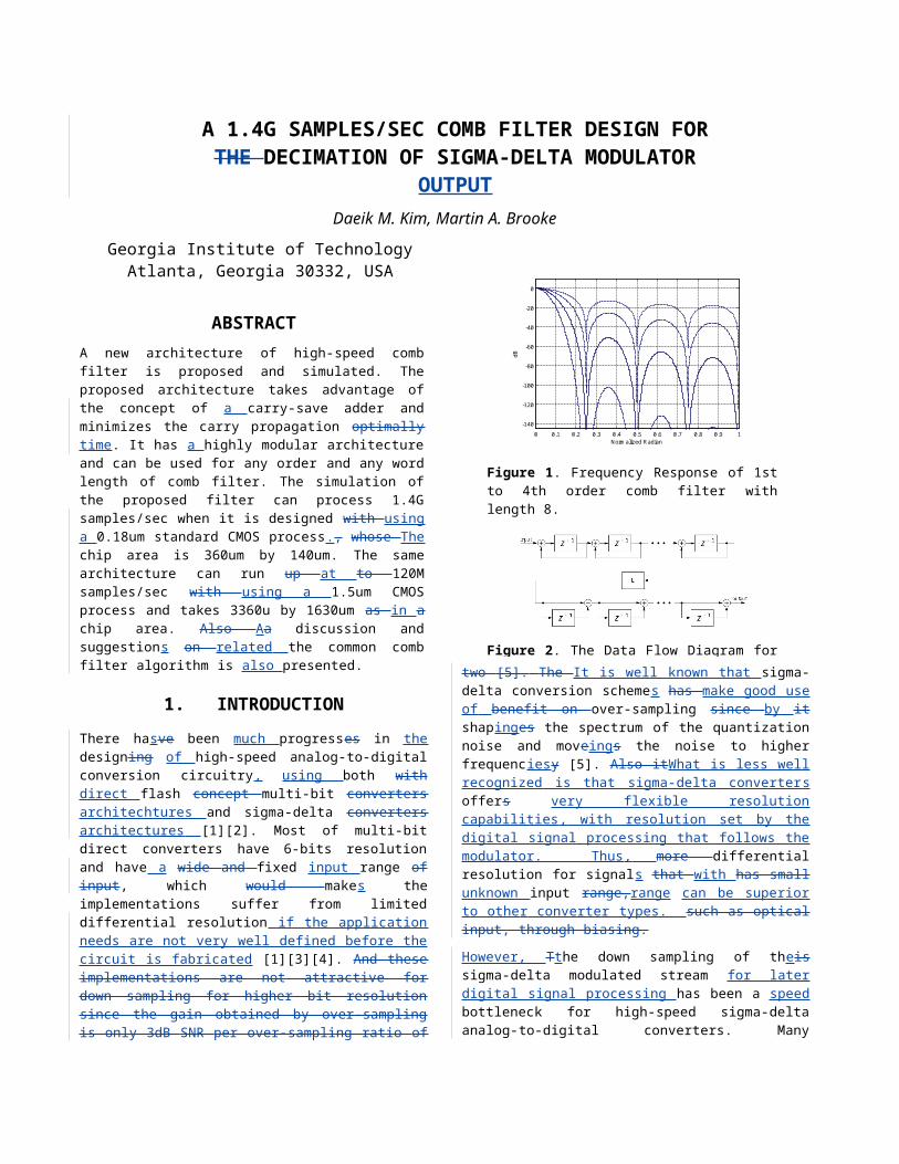
The comb filter was proposed as a down sampling filter for sigma-delta converter due to its simple operation and, linear phase characteristic [5][6]. Figure 1 shows the frequency response of the filter and the attenuation in stop band is good even though the attenuation over the cut-off frequency is not
0 0.1 0.2 0.3 0.4 0.5 0.6 0.7 0.8 0.9 1
-140
-120
-100
-80
-60
-40
-20
0
Normalized Radian
dB
Figure 1. Frequency Response of 1st to 4th order comb filter with length 8.
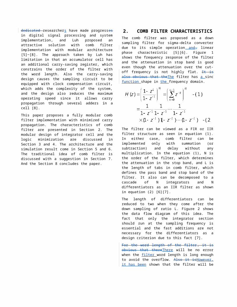
Figure 2. The Data Flow Diagram for the Comb Filter with Down Sampling.
highly flat. It is also obvious that theThe filter has a sinc function shape in the frequency domain.
The filter can be viewed as a FIR or IIR filter structure as seen in equation (1). In either case, comb filter can be implemented only with summation (or subtraction) and delay without any multiplication. In the equation (1), N is the order of the filter, which determines the attenuation in the stop band, and L is the length of tabs in comb filter, which defines the pass band and stop band of the filter. It also can be decomposed to a cascade of N integrators and N differentiators as an IIR filter as shown in equation (2) [6][7].
The length of differentiators can be reduced to two when they come after the down sampling of ratio L. Figure 2 shows the
data flow diagram of this idea. The fact that only the integrator section should run at the sampling frequency is essential and the fast additions are not necessary for the differentiators as a design criterion due to this fact [7].
For the word length of the filter, it is obvious that thereThere will be no error when the filter word length is long enough to avoid the overflow. Also it isHowever, it has been shown that the filter will be functional, if the arithmetic is modular, regardless of the overflow [6].
3. MODULAR CELL DESIGN
The carry save adder can be useful for multi-operand addition especially for the addition of multiplication. What this operation makes expensive is the carry propagation chain goes through the adders at the final stage and the number of operands. The order of this addition algorithm will be
, when n is the word length, the bits used for a value, and k is the number of operands.
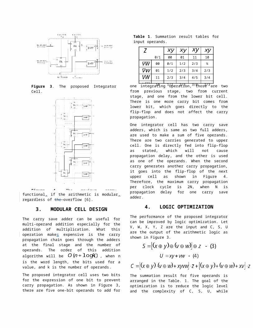
The proposed integrator cell uses two bits for the expression of one bit to prevent carry propagation. As shown in Figure 3, there are five one-bit operands to add for one integrating operation, those are two from previous stage, two from current stage, and one from the lower bit cell. There is one more carry bit comes from lower bit, which goes directly to the flip-flop and does not affect the carry propagation.
One integrator cell has two carry save adders, which is same as two full adders, are used to make a sum of five operands. There are two carries generated to upper cell. One is directly fed into flip-flop as stated, which will not cause propagation delay, and the other is used as one of the operands. When the second carry generates another carry propagation, it goes into the flip-flop of the next upper cell as shown in Figure 4. Therefore, the maximum carry propagation per clock cycle is 2N, when N is propagation delay for one carry save adder.
4. LOGIC OPTIMIZATION
The performance of the proposed integrator can be improved by logic optimization. Let V, W, X, Y, Z are the input and C, S, U are the output of the arithmetic logic as shown in Figure 3.
Figure 3. The proposed Integrator Cell.
Figure 4. The maximum carry propagation path.
Table 1. Summation result tables for input operands.
0/1 00 01 11 10
00 0/1 1/2 2/3 ½
01 1/2 2/3 3/4 2/3
11 2/3 3/4 4/5 3/4
10 1/2 2/3 3/4 2/3
The summation result for five operands is arranged in the Table. 1. The goal of the optimization is to reduce the logic level and the complexity of C, S, U, while maintaining the independence of U from input Z. A set of solution is given in the equation (3), (4), (5) among many possible solutions.
An observation shows that the optimization reduces the normal addition operation by one XOR gate level. The AOI or OAI CMOS logic can be useful in implementation of the solution. Since the equation (3) and (5) has common products of XOR, the logic can be simplified by sharing those products.
5. ARCHITECTURE
The integrator cells can be arranged in a regular layout as shown in Figure 5. The width of the filter, the number of the cells aligned vertically, in Figure 5 and Figure 6, determines the word length, the bits used for a value in the system. The depth of the filter, the number of the cells arranged horizontally, in Figure 5 and Figure 6, determines the order of the filter, N in the equation (1). A block includes capital “I” denotes an integrator, a block with “D” is a differentiator, and a block with “L” is a down sampling circuit with ratio of L, the same L in the equation (1).
The outputs of the integrator are down sampled every L clock cycle and the number format used by integrator is transformed to 2’s complement integer using ripple carry adder since there is enough time for carry propagation after the down sampling. Also all the differentiators are implemented with ripple carry adder. There is an assumption that carry propagation time in differentiation block is less than L times the maximum carry propagation in integration block in this design. This assumption is verified in Section 6. If this assumption is not hold for longer word length, the concept used in the design of the integrator can be applied for the differentiator to prevent carry propagation, which will make the differentiator block take as much chip area as integration block.
6. SIMULATION
The proposed filter architecture wais implemented with 0.18um standard CMOS process rules and the Figure 7 shows the complete layout with functional area description. The word length of the this filter is 16 bits, the order of the filter is 4, and the length of the comb filter is 8. The chip area is 360um by 140um.
A circuit extraction is performed with parasitic capacitance using cadence toolset. The extracted circuit is simulated
Figure 5. The connection diagram of integrator cells.
Figure 6. The outline of the layout for entire system.
Figure 7. The complete layout of the filter.
0 0.02 0.04 0.06 0.08 0.1 0.12-30
-20
-10
0
10
Normalized radian frequency before down sampling
Nor
mal
ized
dB
0 0.02 0.04 0.06 0.08 0.1 0.12-30
-20
-10
0
10
Normalized radian frequency before down sampling
Nor
mal
ized
dB
0 0.02 0.04 0.06 0.08 0.1 0.12-30
-20
-10
0
10
Normalized radian frequency before down sampling
Nor
mal
ized
dB
Figure 8. The output spectrum of comb filter with compared to the spectrum of the pseudo random noise input (top). The comparison of the output spectrum to that of a numerical simulation (center). The comparison of the output spectrum to ideal filter response (bottom).
converted the netlist for in Star Hspice and simulated with pseudo random noise input. The device models is were obtained through MOSIS [ref]. For the verification of the design, samples were taken at the output and the internal nodes in every clock cycle and the voltage values are converted to digital zero or one. A MATLAB script is used for the numerical and functional verification with digitized value from internal nodes and output. Every process stage of integrator and differentiator was examined with the script.
It The simulations shows that the maximum operating frequency of the design is 1.4G samples/sec. The top plot of Figure 8 shows the spectrum of the output of filter when the input to the filter is two thousands bits of pseudo random noise. The spectrum shows that the circuit is working as to the characteristics of the designed comb filter. Also the second part of Figure 8 compares the spectrum of the filter output with the a numerical simulation made by in MATLAB when the input is the same pseudo random sequence. The lower frequency spectrums of both are matching very well and there is’s only a little small deviation, which ist thought to beprobably caused by the limited word length of the filter output. The last plot of Figure 8 compares the output to the ideal response. Also the design is implemented with 1.5um standard CMOS process to show that the maximum operating frequency is 120MHz with 3360u by 1630um chip area.
7. DISCUSSION
It can be noticed in the Figure 8 that the attenuation at the sampling frequency after down sampling, the (1/L of the normalized radian before the down sampling scale), is less than 20dB even though the filter has quite a high order. ThisIt is caused by the fact that down sampling with ratio of L happens between the integrator and the differentiator as shown in Figure 2.
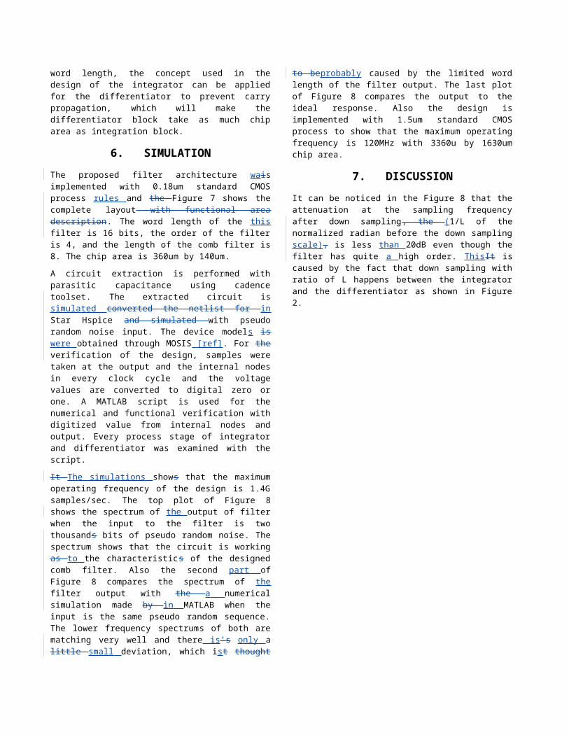
In If case that the a down sampling ratio lower than L is preferred to avoid alias and to take advantage of attenuation over stop band of the filter, L can be reduced to L/2 as in the Figure 2. To support this, the differentiator should have two delays inside it instead of one as shown in Figure 10. It This may cause the carry propagation in differentiation stage is to be too long to fit in L/2 times a clock cycle. If this happens, the differentiator should be designed in the way that the integrator is has been designed in this paper, which will increase the chip area as mentioned in section 5. The frequency response of L and L/2 down sampling is compare in Figure 11. It can be said that L/2 down sampling gives better attenuation since the 1 st
lobe of the comb filter is much lower than the attenuation
provided by the L down sampling case for all order of comb filter.
An implementation of a L/2 concept comb filter is was done with the same 0.18um CMOS process with the a comb filter length of 8. The simulation showed that the maximum operating frequency is still 1.4GHz. The chip area is 380um by 140um, where the additional registers increase size by 20um in one direction. The simulation result is shown in Figure 12.
8. CONCLUSION
Thise paper presentsed the an idea on thea modular integration cells that minimizes the carry propagation of the adder for the comb filter operation. Theseis modular cells were used to
Figure 10. The suggested dataflow diagram for avoiding alias
0 0.02 0.04 0.06 0.08 0.1 0.12-60
-40
-20
0
Normalized Radian
dB
0 0.05 0.1 0.15 0.2 0.25-60
-40
-20
0
Normalized Radian
dB
Figure 11. The comparison of frequency response of L (top) and L/2 (bottom) down sampling with 1st to 4th order comb filter when L=8.
0 0.05 0.1 0.15 0.2 0.25-30
-20
-10
0
10
Normalized radian frequency before down sampling
Nor
mal
ized
dB
0 0.05 0.1 0.15 0.2 0.25-30
-20
-10
0
10
Normalized radian frequency before down sampling
Nor
mal
ized
dB
0 0.05 0.1 0.15 0.2 0.25-30
-20
-10
0
10
Normalized radian frequency before down sampling
Nor
mal
ized
dB
Figure 12. The frequency spectrum of input and output (top). The comparison of the spectrum of the filter output and the numerical simulation (center). The comparison with the ideal response (bottom).
implement simulate implementation of a comb filter with using a 0.18um CMOS process. The maximum operating frequency of the filter was 1.4GHz. Also a down sampling scheme was proposed to improve attenuation and alias of the traditional comb filter implementation.
9. REFERENCES[1] P. Scholtens, M. Vertregt, “A 6b 1.6Gsample/s Flash ADC
in 0.18um CMOS using Averaging Termination,” International Solid-State Circuits Conf erence , 2002, Digest of Technical Papers, Vol. 2, pp. 128-129, 168, 434-435, 456-467.
[2] S. Jaganathan, D. Mensa, T. Mathew, Y. Betser, S. Krishnan, Y. Wei, D. Scott, M. Urteaga, M. Rodwell, “An 18 GHz continuous time sigma delta modulator implemented in InP transferred substrate HBT technology,” 22nd Annual GaAs IC Symposium , 2000, pp. 251-254.
[3] M. Choi, A. A. Abidi, “A 6-b 1.3-Gsample/s A/D Converter in 0.35-um CMOS,” IEEE Journal of Solid-State Circuits, Vol. 36, No. 12, December, pp. 1847–1858, 2001.
[4] C. Donovan, M. P. Flynn, “A “Digital” 6-bit ADC in 0.25-um CMOS,” IEEE Journal of Solid-State Circuits, Vol. 37, No. 3, March, Pp.432-437, 2002.
[5] J. C. Candy, “Decimation for Sigma Delta Modulation,” IEEE Transactions on Communications, Vol. COM-34, No. 1, January, pp.72-76, 1986.
[6] S. Chu, C. S. Burrus, “Multirate Filter Designs Using Comb Filters,” IEEE Transactions on Circuits and Systems, Vol. CAS-31, No. 11, November, pp. 913-924, 1984.
[7] E. Dijkstra, O Nys., C. Piguet, M. Degrauwe, “On the use of Modulo Artithmetic Comb Filters in Sigma Delta Modulators,” Pr o c eedings of the IEEE International Conference on Acoustics, Speech, and Signal Processing, 1988, vol. 4, pp. 2001-2004.
[8] L. Luh, J. Choma, J. Draper, H. Chiueh, “A High-Speed Digital Comb Filter for Sigma-Delta Analog-to-Digital Conversion,” 42nd Midwest Symposium on Circuits and Systems, 2000, vol. 1, pp356 –359.