a 16-b 10msample/s split-interleaved analog to digital ... · a 16-b 10msample/s split-interleaved...
TRANSCRIPT
A 16-b 10Msample/s Split-Interleaved Analog to Digital
Converter
by
Rosamaria Croughwell
A Thesis
Submitted to the Faculty
of the
WORCESTER POLYTECHNIC INSTITUTE
in partial fulfillment of the
Degree of Master of Science
in
Electrical Engineering
August 2007
Approved:
Professor John A. McNeill
Thesis Advisor
Professor Andrew Klein Professor Richard Vaz
Committee Member Committee Member
2
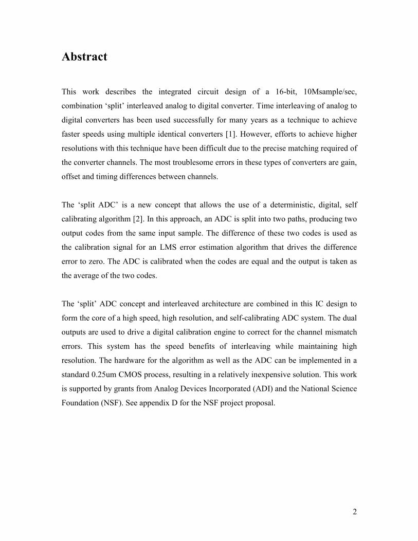
Abstract
This work describes the integrated circuit design of a 16-bit, 10Msample/sec,
combination ‘split’ interleaved analog to digital converter. Time interleaving of analog to
digital converters has been used successfully for many years as a technique to achieve
faster speeds using multiple identical converters [1]. However, efforts to achieve higher
resolutions with this technique have been difficult due to the precise matching required of
the converter channels. The most troublesome errors in these types of converters are gain,
offset and timing differences between channels.
The ‘split ADC’ is a new concept that allows the use of a deterministic, digital, self
calibrating algorithm [2]. In this approach, an ADC is split into two paths, producing two
output codes from the same input sample. The difference of these two codes is used as
the calibration signal for an LMS error estimation algorithm that drives the difference
error to zero. The ADC is calibrated when the codes are equal and the output is taken as
the average of the two codes.
The ‘split’ ADC concept and interleaved architecture are combined in this IC design to
form the core of a high speed, high resolution, and self-calibrating ADC system. The dual
outputs are used to drive a digital calibration engine to correct for the channel mismatch
errors. This system has the speed benefits of interleaving while maintaining high
resolution. The hardware for the algorithm as well as the ADC can be implemented in a
standard 0.25um CMOS process, resulting in a relatively inexpensive solution. This work
is supported by grants from Analog Devices Incorporated (ADI) and the National Science
Foundation (NSF). See appendix D for the NSF project proposal.

3
Acknowledgements
This accomplishment could not have been achieved without the help and support of my
colleagues, family and friends.
First and foremost I would like to thank Professor John McNeill for providing me with
this incredible opportunity. His guidance, support and generosity have made this
academic experience more fun and exciting than I could have imagined. His sense of
humor is an inspiration demonstrating that it is possible to succeed without taking
yourself too seriously.
I would also like to thank Chris David for helping me to understand and use his
calibration algorithm.
Thanks also to the folks in the Precision Nyquist Group at ADI. In particular, I would like
to thank Michael Coln for his advice and mentoring, Gary Carreau for invaluable help
with circuit and layout details and Bruce Amazeen for help with package parasitic
modeling. Most of all, I am grateful to the layout folks: Suhe Gong for getting it started,
Lynn Violette for managing and overseeing it, Dominic Mai for pitching in with the pad
ring, and special thanks to Andrew Shaw who picked this project up as a trainee and
proved himself a natural at this.
Last, but by all means, not least, I want to thank my family and friends. Thanks to my
husband Mike for support, encouragement and patience every step of the way, to my
children Sarah and Jack just for being the great kids that they are and helping out with my
other responsibilities, and to my friends for being there for me.
4
TABLE OF CONTENTS
Abstract ………………………………………………………… 2
Acknowledgements ..…………………………………………… 3
Table of Contents ..…………………………………………..… 4
List of Figures and Tables …………………………………….. 7
1 Introduction ………………………………………………….. 9
2 Background …………………………………………………. 12
2.1 Interleaved ADC Architecture …………………………… 12
2.1.1 Theory of Operation ………………………….… 12
2.1.2 Error Sources for Interleaved Structures ……….…. 13
2.1.2.1 Gain Errors …………………………… 17
2.1.2.2 Timing Errors ………………………… 18
2.1.2.3 Offset Errors ………………………….. 19
2.1.3 Reducing Interleaving Errors ……………………. 20
2.2 Split ADC and Digital Calibration ………………………... 22
2.3 Split-Interleaved ADC Architecture ……………………..... 23
2.3.1 ADC Operation ………………………………... 23
2.3.2 Calibration algorithm …………………………… 24
3 SPLINTA Circuit Design ……………………….……….….. 28
3.1 Overview ……………………….…………………..….. 28
3.1.1 Functional Block Diagram ….……….……….….. 28
3.1.2 SPLINTA I/O Overview ….……….………...….. 29
3.1.3 SPLINTA Operation ….……….…..……......….. 30

5
3.1.4 SPLINTA Timing …..……....……………..… 33
3.1.5 Core ADC Operation ….……….…..……...…. 35
3.1.5.1 SAR ADC Review …….…..……...… 35
3.1.5.2 Charge Redistribution ADC ..……....… 36
3.1.5.3 AD7621 Overview ..……....………… 38
3.1.5.4 AD7621 Timing …..……....………… 39
3.2 SPLINTA Circuit Details …..……....…………….....… 40
3.2.1 Top Level Schematic Diagram ……………...… 40
3.2.1.1 System Noise Issues.……....………… 42
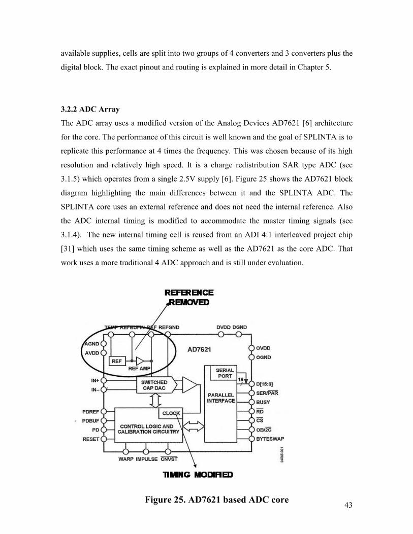
3.2.2 ADC Array …..……....………..……….....… 43
3.2.3 SPLINTA Master Timing Cell …..………......... 44
3.2.4 Digital Block …..………................................ 45
3.2.5 Padring …..………........................................ 46
4 Simulation Results …..………............................................ 48
4.1 Simulation Test Circuit …..………............................... 48
4.2 Functional Simulations …..………............................... 49
4.3 Transistor Level Simulations with Bond Wire Parasitics …. 51
4.3.1 Transistor Level Simulations ............................ 52
4.3.2 Reference Pin Parasitic Simulations ................... 54
4.3.3 Supply Pin Parasitic Simulations ....................... 58
4.4 MATLAB Correction Algorithm ................................... 59
5 Physical Layout and Packaging ...................................... 64
5.1 Physical Layout .......................................................... 64
5.2 Pad Layout ................................................................ 66
5.3 Power Supply Partitioning ........................................... 68
5.3.1 Analog Supplies ............................................ 68
5.3.2 Output Driver Supplies ................................... 68
6
5.3.3 Internal Digital Supply ............................... 69
5.4 SPLINTA Package and Pin List ................................ 69
6 Conclusions ................................................................... 71
6.1 Future Work .......................................................... 72
References ........................................................................ 74
Appendix A Linearity Calibration ....................... 78
Appendix B Evaluation ......................................... 84
Appendix C MATLAB Programs ........................ 86
Appendix D NSF Proposal .................................... 97
7
List of Figures and Tables
Figure 1: 2:1 Interleaving Example ……………………………………………….…… 12
Figure 2: Voltage Errors due to Non-idealities …………….………………….....…… 13
Figure 3: Effect of Input Frequency on Image Spur ...............................................….... 15
Figure 4: Gain-Timing Tradeoff for Image Spur .....................................................….... 16
Figure 5: 4:1 Interleaved ADC with Error Sources Modeled ………………….....…… 17
Figure 6: Output Spectrum of 4:1 Interleaved ADC with Gain Error .....................….... 18
Figure 7: Output Spectrum of 4:1 Interleaved ADC with Timing Error .................….... 19
Figure 8: Output Spectrum of 4:1 Interleaved ADC Simulation with Offset Errors …... 20
Table 1: Comparison of Previous Work ..................................................................….... 21
Figure 9: Split ADC ....................................…………………..……………………...... 22
Figure 10: 2:1 Split-Interleaved Example ...............................................................….... 24
Figure: 11: Error Model ..........................................................................................….... 25
Figure 12: Correction Algorithm ............................................................................….... 27
Figure 13: Functional Block Diagram ............................…………………………….... 29
Table 2: SPLINTA Specifications ..........................................................................….... 30
Figure 14: Simplified Conversion Start Circuit ......................................................….... 31
Figure 15: Simplified SPLINTA Digital Interleaving Circuit ................................….... 32
Figure 16: Valid Data Timing .................................................................................….... 33
Figure 17: Simplified SPLINTA Timing Block Diagram ......................................….... 34
Figure 18: SPLINTA Timing ......................................…………………………….…... 35
Figure 19: SAR ADC Block Diagram ....................................................................….... 36
Figure 20: 3-bit Charge Redistribution DAC .........................................................….... 37
Figure 21: 3-bit Charge Redistribution Example ....................................................….... 38
Figure 22: Simplified AD7621 Architecture ..........................................................….... 39
Table 3: Output Codes ............................................................................................….... 39
Figure 23: SAR Cycle .............................................................................................….... 40
Figure 24: SPLINTA Top Level Schematic Diagram ............................................….... 41
Figure 25: AD7621 Based ADC Core ....................................................................….... 43
Figure 26: Master Timing Block ............................................................................….... 45

8
Figure 27: SPLINTA Digital Block ....................................................................….... 46
Figure 28: PADRING .........................................................................................….... 47
Figure 29: Simulation Test Circuit .....................................................................….... 49
Figure 30: Functional Simulation .......................................................................….... 50
Figure 31: Functional Simulation – 1000 bits ...................................................….... 51
Figure 32: Modeling Level for SPLINTA ADC ................................................….... 52
Figure 33: Flow for Transistor Level Simulation Convergence .………………….... 53
Table 4: Comparison of Simulation Times and Level of Circuit Complexity .……... 54
Figure 34: Bond Wire Model .……………………………………………………..... 54
Figure 35: Original 80-pin SPLINTA Design .…………………………………….... 55
Figure 36: Simulations on Original 80-pin SPLINTA Design with
and without Parasitics .………………………………………………...... 56
Figure 37: Simulation on Original 80-pin SPLINTA Design Reference
tied in Groups of Three .…………………………………………........ .. 57
Figure 38: Separately Pinned Out References ………………………….……........ .. 57
Figure 39: 100-pin Package Simulation Results …………………………..…........ .. 58
Figure 40: Model for MATLAB Calibration ………………………………........... .. 60
Figure 41: Block Diagram for Interleave Simulation with Mismatch Errors ............. 61
Table 5: Induced Error Values .................................................................................... 61
Figure 42: MATLAB Calibration Results .................................................................. 62
Figure 43: MATLAB Convergence ............................................................................ 63
Figure 44: SPLINTA LAYOUT ................................................................................. 65
Figure 45: Chip Pinout ................................................................................................ 67
Table 6: Supply Pads and Connections ....................................................................... 68
Figure 46: SPLINTA Package ..................................................................................... 69
Table 7: Pin List for SPLINTA ................................................................................... 70
9
1 Introduction
The goal for this work was to develop an integrated circuit design for an interleaved ADC
architecture that utilizes the ‘split’ ADC concept [2]. This IC will form the core ADC to
be used with a calibration scheme to achieve 16 bits of resolution at 10Msamples/sec.
High resolution as well as low latency is required in order to be amenable to applications
such as medical imaging, instrumentation and closed loop control systems. Traditional
SAR type converters are popular choices for these types of applications however, they are
currently near or at their speed limit of 4Msamples/s [3, 4]. The ADC design presented
in this thesis is an initial step in breaking through that speed barrier, paving the way for
new advances in these applications. The interleaved architecture together with the ‘split
ADC’ concept provides dual high speed outputs which can be used by an all digital
calibration algorithm to correct for the channel imperfections resulting in a high-speed,
high-resolution ADC system.
Interleaving is a technique introduced over 25 years ago and used to increase the speed of
A/D converters. This method increases ADC throughput without the need for expensive
higher speed process technologies [1]. Existing ADC architectures can be reused with
minimal modifications to build an interleaved system. In general, N converters operate at
a conversion rate of 1/N of a master system clock, each taking turns sampling the input at
equally spaced intervals. The output of each converter is multiplexed to a single system
output producing one seamless code at N times the frequency of any single converter.
Ideally, the resolution of an individual ADC would be preserved. This has proved to be
impossible due to the physical limitations of fabricating perfectly matched converters.
Offset, gain and timing mismatches plague these types of systems causing frequency
domain spurs that reduce the spurious free dynamic range (SFDR), degrading the

10
effective resolution.
A ‘split’ ADC, introduced in 2005, uses the technique of essentially having two ADC’s
simultaneously converting the same sample; producing two output codes [2]. If the
converters were perfectly matched, the two codes would be identical. The difference
between the output codes represents the mismatch and is used as an error signal for the
digital calibration algorithm, which uses an iterative LMS process to drive the errors to
zero. The final output is the average of the two corrected outputs. Since the output is
taken as the average, the ADCs can be physically split in half with minimal impact on
analog area, bandwidth and noise. This technique was used successfully to calibrate the
gain parameter on a 1MSPS, 16-bit cyclic ADC [2]. Appendix D is the NSF proposal
written by Dr. John McNeill which details the ‘split ADC’ concept and project idea.
Combining both the interleaved and split ideas allows this chip flexibility to be used with
a calibration algorithm that corrects for the channel to channel errors of the interleaving,
using the same principles as in the previous work [2, 5]. Unlike the previous work, the
algorithm is more complex because the correction is done for three parameters (offset,
gain, and timing) instead of the single gain parameter. The split is also more complex, as
each ADC in the interleaved array is split and an extra converter is needed in order to
record the errors between all possible pair combinations. For an N:1 interleaved ADC,
2N+1 ADCs are required.
The ADCs were not physically split in this work in order to minimize risk to the main
goal of high resolution at high speed. The core ADC used in this chip is a reused mature
SAR ADC architecture [6] with minimal modifications. While the area benefit is not
realized in this version, a 3dB SNR benefit is expected due to the averaging of the two
corrected outputs [2, 7].
This thesis is organized into six chapters. Chapter 2 provides more detailed background
on the interleaved architecture, the combination split-interleaved ADC architecture and
the digital calibration. Chapter 3 describes the detailed operation and design of the chip
and chapter 4 contains simulation results. Chapter 5 is a description of the physical

11
design of the chip. Lastly chapter 6 outlines the conclusions and future work
recommendations. There are also four appendices. Appendix A describes the linearity
calibration. A schematic diagram for evaluation is shown in Appendix B. Appendix C
contains the MATLAB code used for the time, offset and gain correction. Lastly,
Appendix D is the NSF proposal written by Dr. John McNeill.

12
2 Background
2.1 Interleaved ADC Architecture
2.1.1 Theory of Operation
Time interleaving ADCs is a fairly simple technique for achieving high conversion
speeds. The idea is to use multiple, moderate speed, ADC’s in parallel and combine the
digital outputs to produce a single high-speed output. Figure 1 [5] illustrates the operation
for a simple 2:1 interleaving example. Each ADC samples the same input signal at a rate
of fs/2. ADC1 samples the input at tS1, ADC2 then samples at tS2, 1/fs later while ADC1 is
still working. ADC1 finishes its tS1 conversion sometime between tS2 and tS3 and is ready
for the next sample at tS3. Similarly ADC2 will finish its tS2 conversion in time for tS4.
The two ADC outputs are multiplexed to produce an output code at a rate of fs, twice that
of a single ADC.
ADC1
ADC2
fs/2
fs/2
tS1 tS2 tS3 tS4 tS5
ADC1
ADC2
fs/2
fs/2
tS1 tS2 tS3 tS4 tS5
Figure 1. 2:1 Interleaving Example
13
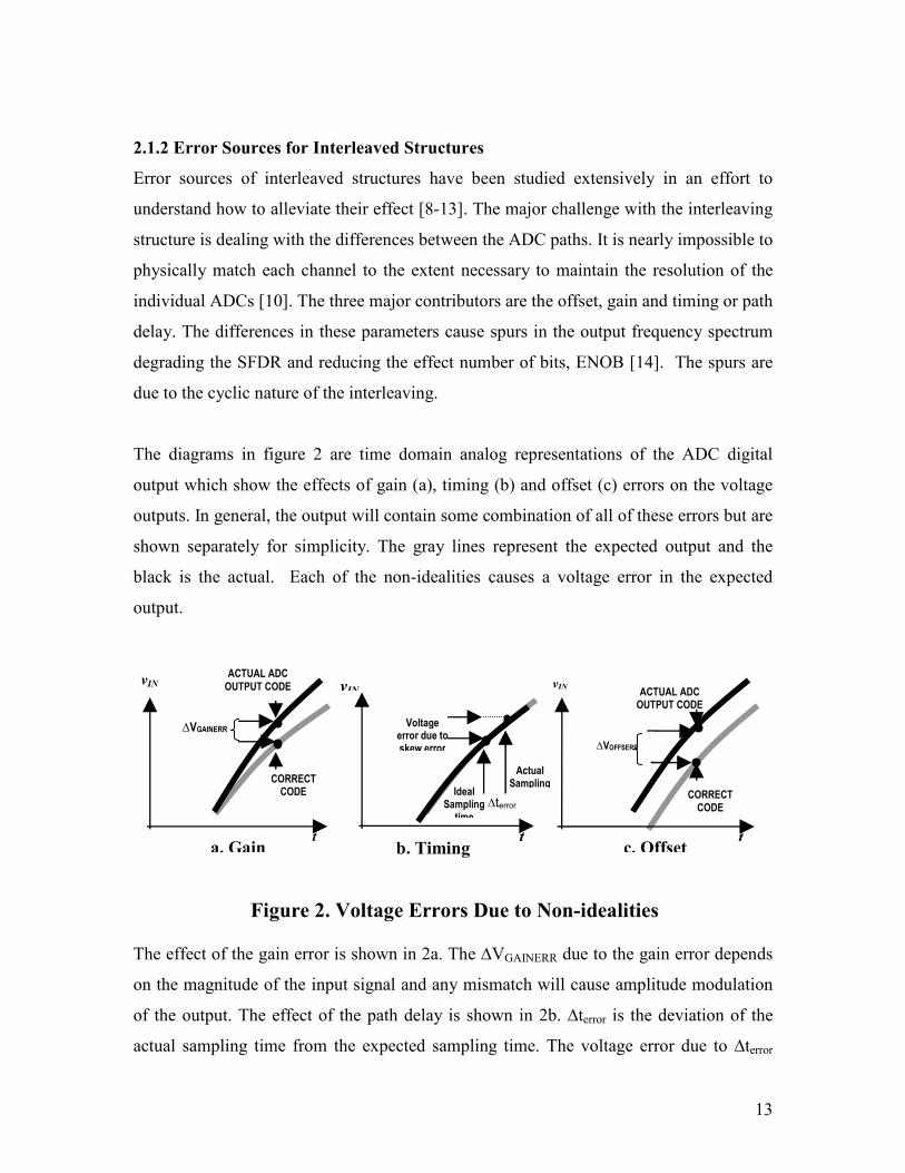
2.1.2 Error Sources for Interleaved Structures
Error sources of interleaved structures have been studied extensively in an effort to
understand how to alleviate their effect [8-13]. The major challenge with the interleaving
structure is dealing with the differences between the ADC paths. It is nearly impossible to
physically match each channel to the extent necessary to maintain the resolution of the
individual ADCs [10]. The three major contributors are the offset, gain and timing or path
delay. The differences in these parameters cause spurs in the output frequency spectrum
degrading the SFDR and reducing the effect number of bits, ENOB [14]. The spurs are
due to the cyclic nature of the interleaving.
The diagrams in figure 2 are time domain analog representations of the ADC digital
output which show the effects of gain (a), timing (b) and offset (c) errors on the voltage
outputs. In general, the output will contain some combination of all of these errors but are
shown separately for simplicity. The gray lines represent the expected output and the
black is the actual. Each of the non-idealities causes a voltage error in the expected
output.
The effect of the gain error is shown in 2a. The ∆VGAINERR due to the gain error depends
on the magnitude of the input signal and any mismatch will cause amplitude modulation
of the output. The effect of the path delay is shown in 2b. ∆terror is the deviation of the
actual sampling time from the expected sampling time. The voltage error due to ∆terror
∆VGAINERR
CORRECT CODE
vIN
t
ACTUAL ADC
OUTPUT CODE
Voltage error due to skew error
vIN
t
Ideal Sampling
time
Actual Sampling
∆terror
∆VOFFSERR
CORRECT CODE
ACTUAL ADC OUTPUT CODE
vIN
t a. Gain b. Timing c. Offset
Figure 2. Voltage Errors Due to Non-idealities

14
depends on the frequency of the input signal. These mismatches will cause phase
modulation. Both gain and timing errors contribute to image spurs at multiples of the
sampling frequency, fs. The converter offset in figure 2c, is a constant voltage error that
does not depend on the input signal. Mismatched offsets cause single tone spurs at
multiples of fs. For a 4:1 interleaved ADC, image spurs will occur at fs/2 - fin, and fs/4 +/-
fin, where fin is the frequency of the input. The offset tones occur at fs/4 and fs/2.
A simple method to relate the size of the errors to the magnitude of the spurs is presented
in [10]. The design equations used for determining the image spurs are given in (1)-(4).
=
2log20 error
GAIN
GSpurIMAGE (1)
scalefull
GAINERRerror
V
VG
∆= (2)
=
2log20 error
PHASESpurIMAGEθ
(3)
errorinerror tf ∆= πθ 2 (4)
These equations can be used to estimate the spur levels given the expected matching. For
example, if the gain accuracy is only expected to match within 0.2%, the spur level can
be expected to be -60dB according to (1).
The effect of the timing errors on the level of the spur depends on the frequency of the
input signal. Equations (3) and (4) are used to calculate the magnitude of a spur due to a
timing mismatch of ∆terror=30ps and is plotted as a function of the input frequency in
figure 3. As the frequency increases, the error becomes more significant as it becomes a
larger portion of the period.

15
Image Spur Magnitude with terror = 30ps
-130.00
-120.00
-110.00
-100.00
-90.00
-80.00
-70.00
-60.00
0.00 1.00 2.00 3.00 4.00 5.00 6.00
Fin [MHz]
Spur [dB]
If both gain and phase difference errors are present, the RMS value of both gives the total
magnitude for the image spurs as given in equation (5).
+
=
22
22log20 errorerror
total
GSpurIMAGE
θ (5)
System level and physical limitations will determine the matching tradeoffs between gain
and timing. Figure 4 shows the combined effect of these mismatches for a 100 kHz and 1
MHz input signal with an image spur of -60dB. For example, if an SDFR of -60dB needs
to be maintained for this frequency range of up to 1MHz and 0.1% gain matching is
expected then, according to figure 4, the path delays need to match to better than 300ps.
The plot illustrates the tradeoffs. Anything below the curve will meet spec, anything
above it will fail.
Figure 3. Effect of Input Frequency on Image Spur

16
The equation for the offset spur is given in (6). In this example, a spur level of -60dB
means that the offsets need to match within 0.1% of the full scale voltage.
∆=
scalefull
OFFSERR
V
VSpurOffset log20 (6)
Gerror (or ∆VGAINERR), θerror (or ∆terror) and ∆VOFFSERR represent the error differences
between each ADC in the system. If the gain error of each ADC is identical, the gain
error difference is zero and will not cause a spur, likewise with the phase and offset
errors.
The block diagram in Figure 5 was used to simulate these effects. Voltage sources are
added to simulate the gain and offset errors. The offsets are modeled by a voltage
VOFFSERRx in the input path to each ADC. The gain error is modeled by the voltage
VGAINERRx in the path of the reference, which sets the full scale voltage. The phase errors
are modeled by placing a time delay, tdelayx in the path of the conversion start pulses.
Gain - Timing Tradeoff for fSFDR=-60dB
0.0000
0.0500
0.1000
0.1500
0.2000
0.2500
0 100 200 300 400 500 600 700 800 900 1000
terror [ps]
Gerror [%
]fin=100kHz
fin=1MHz
Figure 4. Gain-Timing Tradeoff for Image Spurs

17
The values for Gerror, θerror and VOFFSERR are the combined errors, due to each channel,
which appears at DOUTA. Simulation examples of each error effect are described in the
following sections.
2.1.2.1 Gain Error
The effect of mismatched gain was simulated using the model in figure 5. The input to
the ADC is a 2V peak, 140.625 KHz sine wave. The reference voltage, VREFERENCE, is
2.048V and sets the full scale voltage, Vfull scale. The sampling rate, fs, is 12MHz. The
voltages VOFFSERRx, and the delays tdelayx, are set to zero and a gain error is introduced by
intentionally mismatching the reference voltage to each ADC. Figure 6 is the output
frequency spectrum of the analog voltage equivalent of DOUTA, referred to the input.
The spurs that are generated degrade the SFDR to -61dB. This corresponds to a gain error
of 0.18% according to equation (1).
Figure 5. 4:1 Interleaved ADC with Error Sources Modeled

18
The actual values used for VGAINERRx are listed in figure 6. These are arbitrarily selected
to have better than 0.2% matching relative to the mean gain error. This result is slightly
better than predicted by (1) and (5). The simulation is intended only to demonstrate the
effect; the exact values are not relevant. A more rigorous mathematical treatment relating
the individual error contributions to the spur magnitude can be found in several of the
references, [1, 13, 19, 21].
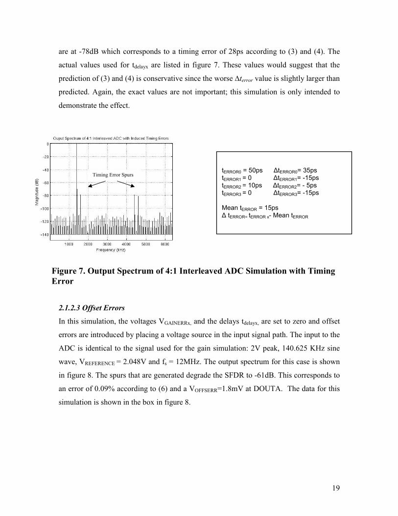
2.1.2.2 Timing Errors
Timing errors occur when the sampling intervals are non-uniform. This is shown in figure
3b where the voltage error depends on the rate of change in voltage, dv/dt, and is more of
a concern at higher frequencies [15]. This can be especially troublesome in interleaved
structures with different delay paths to each ADC. The extent of these errors is generally
due to the physical layout as well as device mismatch.
For this simulation the voltages VOFFSERRx, and VGAINERRx are set to zero. The path delays
are modeled using a delay element, tdelayx, in the path of the conversion start pulses. The
input amplitude, sampling frequency and reference voltage are unchanged from the
previous gain example but the input frequency is increased to 1406.25 KHz to better
demonstrate the effect. The output spectrum for this case is shown in figure 7.The spurs
Figure 6. Output Spectrum of 4:1 interleaved ADC simulation with Gain error
Gain Error Spurs
VGAINERR0 = -5mV ∆GERROR0=-0.18% VGAINERR1 = -3m ∆GERROR1=-0.09% VGAINERR2 = 0mV ∆GERROR2= 0.06% VGAINERR3 = 3mV ∆GERROR3= 0.2% Mean VGAINERR = -1.25mV ∆ VGAINERR= VGAINSERRx- Mean VGAINERR
∆ GERRORx= 100 X ∆VGAINSERRx/Vfull scale
19
are at -78dB which corresponds to a timing error of 28ps according to (3) and (4). The
actual values used for tdelayx are listed in figure 7. These values would suggest that the
prediction of (3) and (4) is conservative since the worse ∆terror value is slightly larger than
predicted. Again, the exact values are not important; this simulation is only intended to
demonstrate the effect.
2.1.2.3 Offset Errors
In this simulation, the voltages VGAINERRx, and the delays tdelayx, are set to zero and offset
errors are introduced by placing a voltage source in the input signal path. The input to the
ADC is identical to the signal used for the gain simulation: 2V peak, 140.625 KHz sine
wave, VREFERENCE = 2.048V and fs = 12MHz. The output spectrum for this case is shown
in figure 8. The spurs that are generated degrade the SFDR to -61dB. This corresponds to
an error of 0.09% according to (6) and a VOFFSERR=1.8mV at DOUTA. The data for this
simulation is shown in the box in figure 8.
Figure 7. Output Spectrum of 4:1 Interleaved ADC Simulation with Timing
Error
Timing Error Spurs
tERROR0 = 50ps ∆tERROR0= 35ps tERROR1 = 0 ∆tERROR1= -15ps tERROR2 = 10ps ∆tERROR2= - 5ps tERROR3 = 0 ∆tERROR3= -15ps Mean tERROR = 15ps ∆ tERROR= tERROR x- Mean tERROR

20
2.1.3 Reducing Interleaving Errors
With technologies shrinking to deep sub micron levels, channel matching on interleaved
structures becomes even more difficult. Moving as much functionality as possible to the
digital domain, and minimizing analog complexity, makes sense from both a cost and
performance standpoint [16]. Much effort has gone into addressing this issue [5, 8-13, 16-
20].
Spurs generated by offset and gain mismatches are a result of the repeating ADC
selection pattern of the interleaving. This can be alleviated by randomizing the selection
pattern [8, 11, 17]. At least one extra channel must be added to enable random selection.
This technique decorrelates the samples and eliminates the spurs but at the expense of
raising the noise floor. This simple solution may be acceptable for some applications, but
is not precise.
Some solutions for the correction of the timing skews are implemented by the addition of
a calibration signal [12, 9]. A ramp with a known slope is used to measure the timing for
each ADC. A digital interpolator uses the information to calculate the corrections
VOFFSERR0 = 0 ∆VOFFSERR0=-0.125 VOFFSERR1 = -2m ∆VOFFSERR1=-1.875 VOFFSERR2 = 1.5mV ∆VOFFSERR2= 1.375 VOFFSERR3 = 1mV ∆VOFFSERR3= 0.875 Mean VOFFSERR = 0.125mV ∆ VOFFSERR= VOFFSERRx- Mean VOFFSERR
Figure 8. Output Spectrum of 4:1 interleaved ADC simulation with offset
errors
Offset Error Spurs

21
necessary to eliminate the skew between channels. The approach in [9] limits the
dynamic range which is circumvented in [12] by adding an extra calibration channel.
A randomly controlled chopper front end approach is used in [18-21] to extract offset and
gain information. The input is transformed to a noise signal by a chopper sample and hold
front end, controlled by a PRBS, then digitized by the ADC. The offset and gain errors
are estimated digitally by calculating the mean and variance every N samples of the
output code. The original signal is then reconstructed using the same PRBS, including the
corrections. The corrections are updated every N samples. A single front rank SHA is
used in [19]. This eliminates the timing skew issues but limits the speed of the system. A
separate chopper SHA for each channel is used in [13, 19-21] and the timing skew
between samples is estimated and corrected with filtering. These approaches rely on the
statistics of the input signal and can have limitations on the input frequency. They also
require added complexity in the analog portion.
A split ADC approach can be applied to an interleaved structure to provide dual outputs
which can be used with a calibration algorithm to correct for offset and gain as well as
timing errors [2, 5]. The all digital algorithm requires no additional analog complexity,
needs no special calibration signal, and runs continuously in the background. Table 1 lists
issues that are addressed by the split-interleaved, self-calibrating ADC system, and
compares them with previous work.
[8] [9] [10] [11] [12] [13] [17] [18] [19] [20]
Offset 1 1 3
Gain 1 1 3 2
Timing 1 2,3 1 1
All Digital Calibration 4 4 4 4
Deterministic
Background Calibration
Self-Calibration
1 Improvement by speading out the spurs - does not eliminate
2 Trouble at some input frequencies
3 Limited input range
4 Added analog complexity
Table 1 Comparison of Previous Work
22
2.2 Split ADC and Digital Calibration
The split ADC concept, introduced in 2005[2], uses two independent ADCs, each
converting the same input sample. The work described in [2] was for a cyclic ADC in
which only the gain parameter needs correction (Appendix D). The difference of the two
outputs is used as a calibration signal for the correction algorithm. The overall output is
taken as the average of the two corrected outputs. Convergence is fast compared with
other probabilistic methods [22-26] since the unknown input signal is eliminated from the
calibration signal path which drives the correction algorithm. Moving these complex
calibrations entirely to the digital domain relieves some of the burden on the analog
complexity as well as lowers the cost.
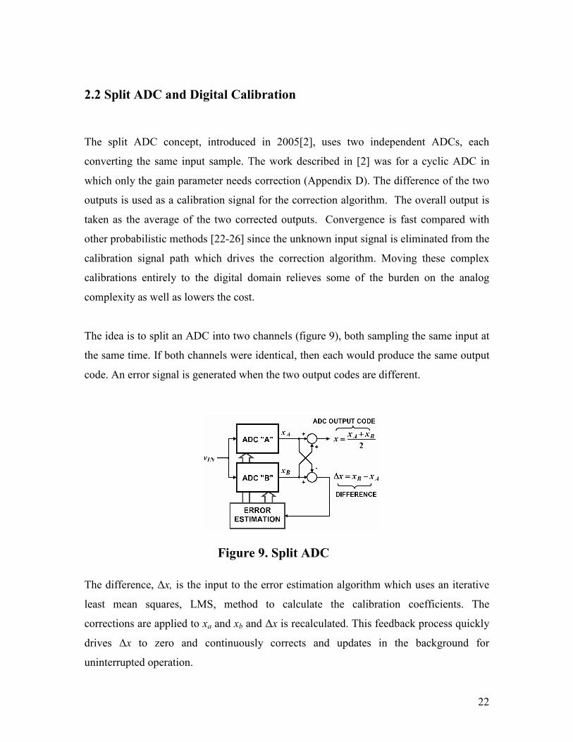
The idea is to split an ADC into two channels (figure 9), both sampling the same input at
the same time. If both channels were identical, then each would produce the same output
code. An error signal is generated when the two output codes are different.
The difference, ∆x, is the input to the error estimation algorithm which uses an iterative
least mean squares, LMS, method to calculate the calibration coefficients. The
corrections are applied to xa and xb and ∆x is recalculated. This feedback process quickly
drives ∆x to zero and continuously corrects and updates in the background for
uninterrupted operation.
Figure 9. Split ADC
23
The ADC output code is taken as the average of the corrected xA and xB outputs. This
digital averaging has the benefit of improving the SNR by a factor of 2 [2, 7].
However, the original concept of a ‘split ADC’ is to essentially halve the analog area for
a given ADC design with certain power, speed and noise specifications. Since the area is
split, the capacitors are halved and the kt/C noise is increased by 2 but because of the
averaging of the output, that factor is removed and the noise is unchanged. The active
circuits are also halved such that the bandwidth (gm/C) and the power are unchanged.
This concept has been proven successfully on a 16bit 1Msample/second cyclic converter
[2]. The calibration technique is independent of the type of converter used and combines
the cost benefits of an all digital implementation and the speed benefits of the
deterministic nature (tracking out errors continuously, quickly), completely performed in
the background without interrupting the conversions.
2.3 Split- Interleaved ADC
2.3.1 ADC Operation
The ‘split ADC’ idea can be extended to the more complicated interleaved architecture.
In addition to the gain parameter targeted in the previous work, the offset and timing
parameters can also be calibrated. Each ADC in the interleaved array must be split and an
additional ADC needs to be added in order to calculate the ∆x between every possible
ADC pair. For an M:1 interleave, 2M+1 ADCs are needed for this type of calibration. For
example, a 2:1 split interleaved ADC (Figure 10) requires 5 ADCs.
The basic difference from the traditional interleaved ADC described in section 2.1.1, and
the split-interleaved structure in figure 10 is that, in this case, a pair of ADC’s are
selected to convert the same sample instead of a single converter. The operation is very
similar to the previous case. The sample rate for the system is fs and each individual ADC

24
samples at fs/2. Initially, ADC “A” and ADC “B” sample the input at tS1. At 1/fs later,
ADC “C” and ADC “D” sample at tS2 while ADC “A” and ADC “B” are still working on
tS1’s conversion. ADC “A” and ADC “B” become available again sometime between tS2
and tS3. Notice that in the absence of ADC “E”, the only next possible combination for tS3
is ADC “A” and ADC “B” again because ADC “C” and ADC “D” are still working on
tS2’s conversion. ADC “E” is required since the A-C, A-D, B-C, and B-D pairs are not
possible without it and the errors for all the possible paths must be computed for the
calibration to work. ADC “E” also enables randomization of the ADC selection which
eliminates the spurs due to the mismatch errors [8, 11, 17]. The five ADC outputs are
sorted by the digital block and assembled into the two channels, xDOUTA and xDOUTB, each
producing output codes at the rate of fs. These outputs drive the calibration algorithm that
will correct for the interleave array mismatch errors between channels.
Figure 10. 2:1 Split-Interleaved Example
2.3.2 Calibration Algorithm
The calibration algorithm described here addresses the errors associated specifically with
the interleaved structure due to the mismatches between ADCs. The linearity calibrations
of each individual ADC is handled separately and described in Appendix A.
ADC “A”
ADC “B”
ADC “C”
ADC “D”
ADC “E”
DIGITAL
xD
xE
vIN
xA
xB
xC xDOUTB
xDOUTA
xDOUTA, xDOUTB
tS1 tS2 tS3 tS4 tS5

25
The same iterative approach demonstrated in the previous work [2] is applied in this case.
The calibration algorithm for the interleaved design is more complex since the number of
parameters to correct for is increased to three. As described in section 2.1.2, these errors
can cause spurs in the frequency spectrum degrading the SFDR. To further complicate
the algorithm, the three parameters must be calculated for each pair combination. In a 2:1
split interleaved ADC, there are a total of 5 ADCs with 10 possible pair combinations.
The error model in figure 11 is used to define the ADC output [5] with the three error
sources from figure 3 combined. The output, xDOUT, is comprised of the ideal value, x,
plus the error terms for offset, gain and timing delay and is modeled by equation (a) in
the figure.
Figure 11. Error Model
The correction algorithm uses the difference between each combination of interleaved
pairs to calculate, xos, Ge and et using an LMS process. In figure 10, the interleaved
outputs are xDOUTA and xDOUTB and can be any pair combination of xA through xE. The two
outputs can be expressed by (7) and (8) where x is the desired output.
vout
videal
te APERTURE
DELAY ERROR
xOS, x.Ge
OFFSET,
GAIN ERRORS
CORRECT
CODE
xADCACTUAL ADC
OUTPUT CODE
x
vIN
t
444 3444 21
ERRORS
dt
dxtGxx
CODECORRECT
xx eeOSADC
+⋅++=
x
444 3444 21
ERRORS
OS
CODECORRECT
DOUTdt
dxteGexxxx
+•++= (a)
DOUT
te APERTURE
DELAY ERROR
xOS, x.Ge
OFFSET,
GAIN ERRORS
CORRECT
CODE
xADCACTUAL ADC
OUTPUT CODE
x
vIN
t
444 3444 21
ERRORS
dt
dxtGxx
CODECORRECT
xx eeOSADC
+⋅++=
x
444 3444 21
ERRORS
OS
CODECORRECT
DOUTdt
dxteGexxxx
+•++= (a)
DOUT

26
444444 3444444 21termserror
eDOUTAeDOUTAosDOUTADOUTAdt
dxtGxxxx +•++= (7)
444444 3444444 21termserror
eDOUTBeDOUTBosDOUTBDOUTBdt
dxtGxxxx +•++= (8)
The error between the two outputs is given by (9). The x term is eliminated and all that is
left are the error terms.
eDOUTBeDOUTAe
eDOUTBeDOUTAe
osDOUTBosDOUTAos
eeosDOUTBDOUTA
ttt
GGG
xxx
dt
dxtxGxxxx
−=∆
−=∆
−=∆
∆+•∆+∆=−=∆
(9)
Data is collected in a matrix for all possible pair combinations of the ADCs. An LMS
method is used in a negative feedback process to estimate the corrections necessary to
drive (9) to zero [2, 5]. The corrected output is given by (10). The final ADC output is
the average of DOUTAx)
and DOUTBx)
.
+•+−==
dt
dxtxGxxxx DOUTeDOUTeosDOUTDOUTBDOUTA
)) (10)
Since the timing error term includes a derivative, two points are needed for this
calculation and are taken from two adjacent samples. A 1 sample latency penalty is
necessary for this calculation [5].
The block diagram for the correction algorithm is shown in figure 12. The uncorrected
codes, as well as the tag marking which ADC they are from, are collected from the ADC
output. The derivative is approximated and stored in the estimation matrix. A digital
correction is applied and xa and xb are recalculated. New values for x and ∆x are
calculated and stored in the estimation matrix. The algorithm then iterates around the
shaded loop, constantly updating the estimates driving the error between the codes less

27
than the tolerance set by the algorithm and maintaining that level during operation of the
system.
Figure 12. Correction Algorithm.
This correction method converges in less than 200K conversions. It is fast because it does
not rely on statistics for the correction information. The system is continuously updating
the correction coefficients, tracking out errors that could develop over time due to factors
such as temperature and power supply variations. The ‘corrected’ output code will
converge with an overall offset and gain error, but this is easily compensated in post
processing. A more rigorous explanation of the algorithm can be found in Appendix D
and [5].

28
3 SPLINTA Circuit Design
3.1 Overview
SPLINTA is a SAR based 4:1 split-interleaved ADC integrated circuit design. This chip
targets 16 bits of resolution at 10MHz. It is specifically designed to be used with the
digital calibration algorithm described in section 2.3.2, currently being developed at WPI.
The technology for this project is a 0.25um CMOS process with 5 levels of metal. The
size is approximately 7mm on a side and it will be packaged in a 100 pin LQFP package.
3.1.1 Functional Block Diagram
The functional block diagram for the complete self-calibrating ADC system is shown in
figure 13. The FPGA contains the hardware for the correction algorithm as well as the
clock signals for the ADC. SPLINTA is the IC design for the ADC portion of this system
and is highlighted in the shaded area. The 4:1 interleaving requires 9 ADCs (section
2.3.1) in order to perform both interleave and split. The timing logic generates the signals
that control the SAR cycles. The MUX is used to send the conversion start pulse,
CNVST, to the appropriate ADC pair according to the selection lines, SELA and SELB,
which is controlled by the FPGA. The digital output blocks assemble the codes from the
individual ADCs and provide the dual high speed outputs, DOUTA and DOUTB, along
with their identifiers, TAGA and TAGB. These outputs are processed by the correction
algorithm within the FPGA providing the calibrated output, DOUT.

29
ADC0
ADC1
ADC8SIG IN
SEL ADC A
MASTER CLOCK
SYNC
100MHzTiming Logic
SAR TIMING
10MHz
MUX
READ B
DIGITAL
OUTPUT
BLOCKS
CNVST
DOUT
DOUTCNVST
DOUTB
DOUTA
TAGB
BUSYB
SEL ADC B
TAGA
REFERENCE
READ A
CNVST
BUSYA/B
CNVSTDOUT
BUSYA/B
BUSYA/B
CALIBRATION MODE SIGNALS
BUSYA
DOUTFPGA
CORRECTION ALGORITHM
CLOCK SIGNALS
ADC OUTPUTS
AND IDENTIFIERS
ADC SELECTION
AND CLOCKS
ADC CORRECTED
OUTPUT
SPLINTA
Figure 13. Functional Block Diagram
3.1.2 SPLINTA I/O Overview
The CALIBRATION MODE SIGNALS and the BUSYA, BUSYB outputs are mainly
used for the individual ADC linearity calibration (Appendix A). The BUSYx signals can
also be used as a ‘data ready’ indicator (see section 3.1.3).
The input, SIG IN, is differential and common to all ADCs. The external reference is also
common to each ADC but pinned out separately on the package for maximum isolation
(see section 4.3). The SAR TIMING is derived from an external MASTER CLOCK
which is intended to run at a frequency of 100MHz, but can be slowed for debug and
evaluation purposes. The timing logic provides the signals which control the timing of the
sample and acquire phases of the SAR ADCs. It also provides the SAR bit cycling clock
for each ADC. The external SYNC pulse is synchronized internally with the SAR bit
cycling clock and used to generate the conversion start pulses, CNVST. This signal is
intended to run at 10MHz and can be adjusted, independently of the master clock.
30
Adjusting the sampling rate can also be useful for debug and evaluation purposes. A
multiplexer cell sends the CNVST pulse to two of the 9 ADC’s according to the 4 bit
ADC selection busses, ‘SEL ADC A’ and ‘SEL ADC B’. The outputs are two 16 bit wide
data busses for the A and B channels plus two 4 bit identifiers to mark which ADC the
data came from. This information can be used by the FPGA and is also useful for
evaluation and debug. The data from each ADC appears at the output 4 conversion pulses
after its conversion start (Figure 15).
At the heart of SPLINTA is the AD7621 16-bit, 3MSPS PulSAR ADC architecture. The
goal of the correction algorithm is to remove all interleaving errors enabling the same
performance as the AD7621 [6] at 4 times the speed. Table 2 summarizes some of the
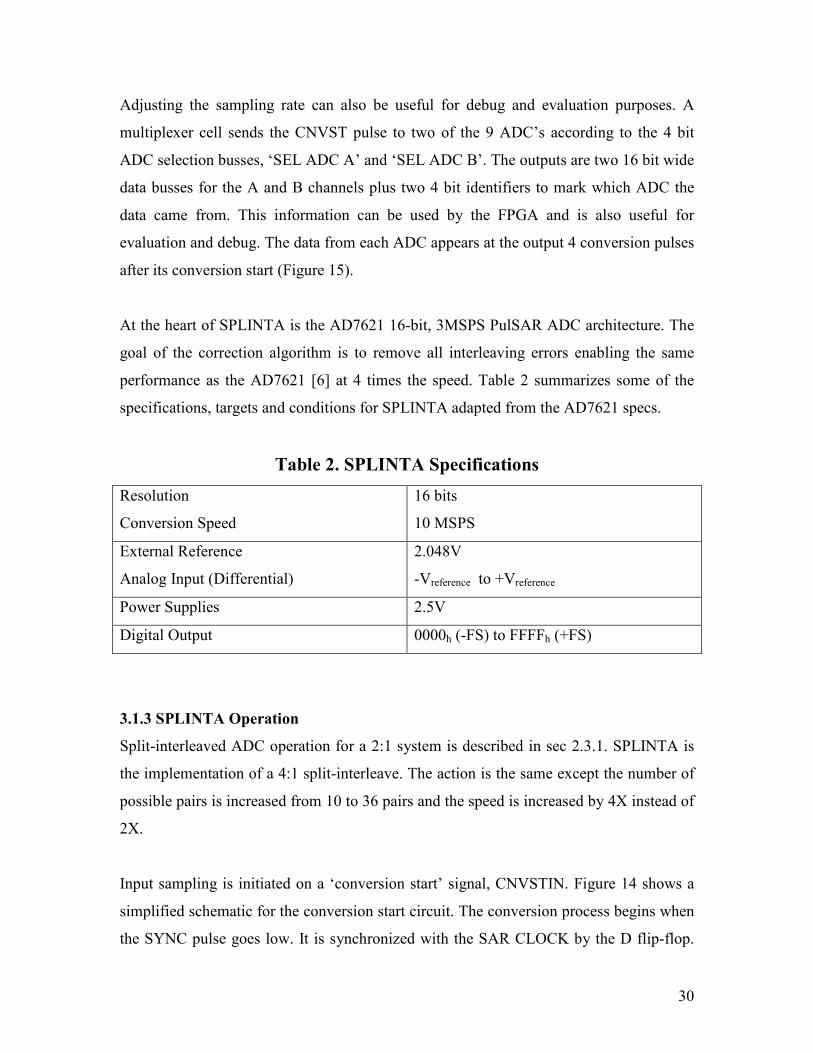
specifications, targets and conditions for SPLINTA adapted from the AD7621 specs.
Table 2. SPLINTA Specifications
Resolution
Conversion Speed
16 bits
10 MSPS
External Reference
Analog Input (Differential)
2.048V
-Vreference to +Vreference
Power Supplies 2.5V
Digital Output 0000h (-FS) to FFFFh (+FS)
3.1.3 SPLINTA Operation
Split-interleaved ADC operation for a 2:1 system is described in sec 2.3.1. SPLINTA is
the implementation of a 4:1 split-interleave. The action is the same except the number of
possible pairs is increased from 10 to 36 pairs and the speed is increased by 4X instead of
2X.
Input sampling is initiated on a ‘conversion start’ signal, CNVSTIN. Figure 14 shows a
simplified schematic for the conversion start circuit. The conversion process begins when
the SYNC pulse goes low. It is synchronized with the SAR CLOCK by the D flip-flop.

31
The synchronized output, CNVSTIN, is used to ensure sampling at the beginning of the
bit decision cycle where digital noise is less likely to cause a bit decision error elsewhere
in the array. The 4 bit addresses on the SELA and SELB lines determine which pair of
ADCs is selected to sample. A new pair of ADCs is selected every 1/fsample seconds but
each ADC must have a minimum of 4 conversion times (4/ fsample) to complete its
conversion, before it can be selected again. The waveforms in figure 14 illustrate the
timing. Initially, in this example, ADC0-1 pair is selected and the CNVSTIN pulse is
routed to CNVSTB0, and CONSTB1. It then cycles through pairs ADC2-3, ADC4-5 and
ADC6-7. By the 5th conversion pulse, ADC0 and ADC1 are finished their conversion
and ready for the next sample. Either ADC0 or ADC1 can be paired with the ‘spare’
ADC8 for the next sample. By the 6th conversion ADC2, ADC3 and ADC4 are available
and a new pair can be selected, and so forth. The pairs are randomly selected from the
three available each conversion cycle. The selection process can be controlled manually
for evaluation or by the digital processor that contains the calibration algorithm.
Figure 14. Simplified Conversion Start Circuit
Figure 15 is a simplified schematic diagram of the digital interleaving circuit. The nine
16-bit digital output busses from each converter is sorted and assembled into two high
speed digital outputs by a multiplexer array. READ A and READ B words selects which
pair of ADC outputs is ready and are generated by shifting the SELA and SELB words
over by 4 conversion times or 4/fsample. The READ busses are also used as the ADC
identifiers, TAGA and TAGB. The waveforms in figure 15 demonstrate this action. The
sequence starts with the ADC pair 0-1 selected to start conversion on the first sample.
This is followed by the pairs 2-3, 4-5, and 6-7, etc. Four conversion pulses after the
ADC0-1 start, the READA-B busses signal the results of the conversions, DOUT0 and
D
CK
Q
SYNC
SAR
TIMING
CNVSTIN
MASTER
CLOCK
SAR
CLOCK
TO ADCs
SAR CLK
CNVSTIN
SELA 0 2 4 6 8 1 3 5 7
SELB 0 1 3 5 7 0 2 4 6 8
CNVSTB0
CNVSTB1
CNVSTB2
CNVSTB3
CNVSTB4
CNVSTB5
CNVSTB6
CNVSTB7
CNVSTB8
1.9 1.95 2 2.05 2.1 2.15 2.2 2.25 2.3 2.35 2.4 2.45 2.5 2.55 2.6 2.65 2.7 2.75time, uSeconds
32
DOUT1 (8000h) to be sent to the outputs, DOUTA and DOUTB. Note the individual
ADC outputs, DOUT0-DOUT8 are converting at one quarter the rate of the two main
outputs, DOUTA and DOUTB. This quadrupling of the ADC speed is the major benefit
of the interleaving structure.
Figure 17. Simplified SPLINTA Digital Interleaving Circuit
The CNVSTBIN pulse is generated from the external SYNC pulse and can be used to
signal when data is ready. The output data is valid from the rising edge of the
CNVSTBIN pulse to the falling edge of the next CNVSTBIN pulse.
The waveforms in figure 16 show the timing for valid output data. In this example, the
SAR clock is 96MHz and the sample clock is 12MHz. CNVSTBIN is the external SYNC
pulse (not to be confused with CNVSTIN, the synchronized version). The pulsewidth is
approximately the width of a SAR clock cycle, ~10ns. The falling edge of this pulse
initiates a conversion cycle as well as controls when the ADC outputs appears at the
interleaved output as described above. The data is valid until the next falling edge of
CNVSTBIN when the next sample is routed to the output. The ideal sample point is
midway between these edges. The rising edge of this pulse should be sufficient to signal
valid data as long as the pulse at least as wide as shown in figure 16.
The BUSYA and BUSYB signals are normally used for the linearity calibration
(Appendix A). However, it is possible to use this output in normal mode to signal valid
data as well. During normal operation, the busy signals from the nine ADCs are
multiplexed to the outputs, BUSYA and BUSYB, according to the SELA and SELB
lines. Initially, when a new ADC pair is selected, the BUSY signals from the new pair
Figure 15. Simplified SPLINTA Digital Interleaving Circuit
33
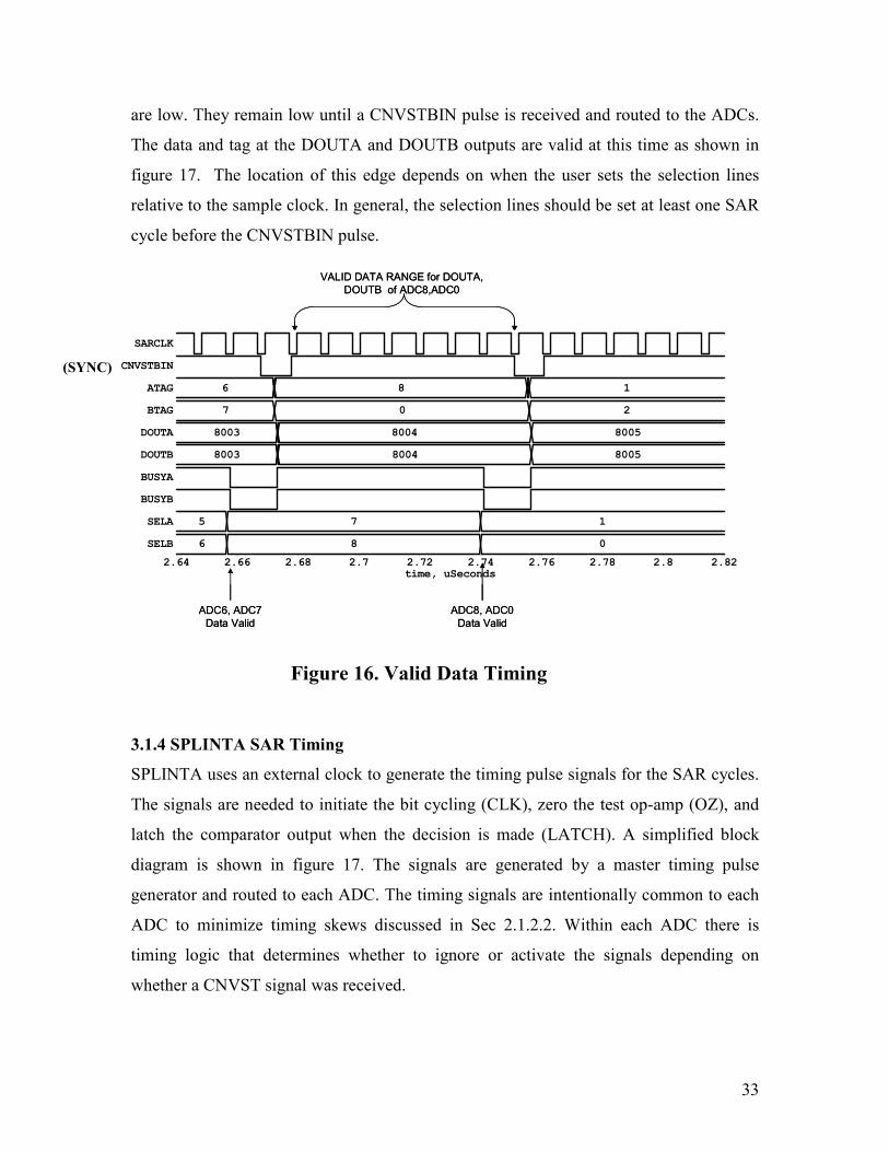
are low. They remain low until a CNVSTBIN pulse is received and routed to the ADCs.
The data and tag at the DOUTA and DOUTB outputs are valid at this time as shown in
figure 17. The location of this edge depends on when the user sets the selection lines
relative to the sample clock. In general, the selection lines should be set at least one SAR
cycle before the CNVSTBIN pulse.
3.1.4 SPLINTA SAR Timing
SPLINTA uses an external clock to generate the timing pulse signals for the SAR cycles.
The signals are needed to initiate the bit cycling (CLK), zero the test op-amp (OZ), and
latch the comparator output when the decision is made (LATCH). A simplified block
diagram is shown in figure 17. The signals are generated by a master timing pulse
generator and routed to each ADC. The timing signals are intentionally common to each
ADC to minimize timing skews discussed in Sec 2.1.2.2. Within each ADC there is
timing logic that determines whether to ignore or activate the signals depending on
whether a CNVST signal was received.
Figure 16. Valid Data Timing
VALID DATA RANGE for DOUTA,
DOUTB of ADC8,ADC0
SARCLK
CNVSTBIN
ATAG 6 8 1
BTAG 7 0 2
DOUTA 8003 8004 8005
DOUTB 8003 8004 8005
BUSYA
BUSYB
SELA 5 7 1
SELB 6 8 0
2.64 2.66 2.68 2.7 2.72 2.74 2.76 2.78 2.8 2.82time, uSeconds
ADC6, ADC7
Data Valid
ADC8, ADC0
Data Valid
VALID DATA RANGE for DOUTA,
DOUTB of ADC8,ADC0
SARCLK
CNVSTBIN
ATAG 6 8 1
BTAG 7 0 2
DOUTA 8003 8004 8005
DOUTB 8003 8004 8005
BUSYA
BUSYB
SELA 5 7 1
SELB 6 8 0
2.64 2.66 2.68 2.7 2.72 2.74 2.76 2.78 2.8 2.82time, uSeconds
ADC6, ADC7
Data Valid
ADC8, ADC0
Data Valid
(SYNC)

34
Figure 18 shows the timing signals of a conversion cycle for ADC0 and ADC2. The
MASTER CLOCK drives the timing pulse generator and produces the MASTER OZ and
MASTER LATCH pulses which run continuously and are routed to each ADC. The
SELA bus routes the MAIN CNVST pulse to the appropriate ADCs and signals the
timing block to pass the timing pulses. In figure 18, a CNVSTB0 pulse activates the
timing for ADC0 and the CLK, OZ and LATCH pulses are routed to the CAP DAC.
ADC2 timing remains inactive until a CNVSTB2 pulse is received at which time the
signals are routed to both ADC0 and ADC2. The ADC0 signals remain active until the
end of the bit cycling where it then goes into a wait mode for the next CNVSTB0 signal.
MASTER
CLOCK
100MHZ
ADC0
ADC2
ADC8
ADC
TIMING
ADC
TIMING
ADC
TIMING
TIMING PULSE
GENERATOR
MAIN CNVST
CNVSTB0
CNVSTB2
CAP
DAC
CAP
DAC
CAP
DAC
MASTER
CLOCK
MASTER OZ
MASTER
LATCH
CLK0
OZ0
LATCH0
CLK2
LATCH2
OZ2
Figure 17. Simplified SPLINTA Timing Block Diagram

35
3.1.5 CORE ADC Operation
The core ADC used in the array is a 16-bit 3MSPS SAR type ADC. This is, by far, the
most critical circuit in SPLINTA. The architecture of the ADC core is reused from the
Analog Devices AD7621 [6] with some slight modifications. This SAR ADC was
chosen because of its high resolution and decent speed. Using a proven design minimizes
the risk to the overall architecture.
3.1.5.1 SAR ADC Review
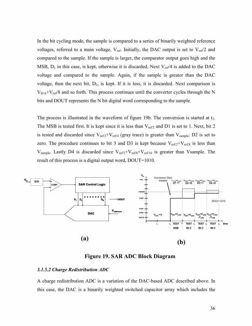
A block diagram for a DAC-based successive approximation A/D converter is shown in
Figure 19a [27]. This type of ADC is named for the algorithm used for the conversion,
which is based on a binary search method. There are three phases to a typical SAR
conversion cycle: sample, hold and bit cycling.
The input to the ADC is generally a sample and hold circuit. The converter is in ‘acquire’
or ‘sample’ mode until a conversion is initiated. In sample mode, the input is simply
monitored, waiting for a ‘start’ signal. Once a conversion start signal is received, the S/H
circuit switches to hold mode so that the sample value doesn’t change during the
conversion process.
Figure 18. SPLINTA Timing
MAIN CNVST
SELA 0 2 4 6 8
MASTER CLOCK
MASTER OZ
MASTER LATCH
CNVSTB0
CLK0
OZ0
LATCH0
CNVSTB2
CLK2
OZ2
LATCH2
2 2.04 2.08 2.12 2.16 2.2 2.24 2.28 2.32time, uSeconds
36
In the bit cycling mode, the sample is compared to a series of binarily weighted reference
voltages, referred to a main voltage, Vref. Initially, the DAC output is set to Vref/2 and
compared to the sample. If the sample is larger, the comparator output goes high and the
MSB, D1 in this case, is kept, otherwise it is discarded. Next Vref/4 is added to the DAC
voltage and compared to the sample. Again, if the sample is greater than the DAC
voltage, then the next bit, D2, is kept. If it is less, it is discarded. Next comparison is
VD/A+Vref/8 and so forth. This process continues until the converter cycles through the N
bits and DOUT represents the N bit digital word corresponding to the sample.
The process is illustrated in the waveform of figure 19b. The conversion is started at t2.
The MSB is tested first. It is kept since it is less than Vref/2 and D1 is set to 1. Next, bit 2
is tested and discarded since Vref/2+Vref/4 (gray trace) is greater than Vsample: D2 is set to
zero. The procedure continues to bit 3 and D3 is kept because Vref/2+Vref/8 is less than
Vsample. Lastly D4 is discarded since Vref/2+Vref/8+Vref/16 is greater than Vsample. The
result of this process is a digital output word, DOUT=1010.
3.1.5.2 Charge Redistribution ADC
A charge redistribution ADC is a variation of the DAC-based ADC described above. In
this case, the DAC is a binarily weighted switched capacitor array which includes the
S/H +
-COMP
Vin
SAR Control Logic
DAC
DOUTD1 D2 DN
Vreference
S/H +
-COMP
Vin
SAR Control Logic
DAC
DOUTD1 D2 DN
Vreference
Figure 19. SAR ADC Block Diagram
(a) (b)
Vref
Vref/8
time
Vin
TEST
Bit 4
TEST
MSB
TEST
Bit 2
TEST
Bit 3
Conversion Start
Initiated VD/Atest<Vsample
D1 =1VD/Atest >Vsample
D2 =0
t1 t2t3 t4 t5 t6
VD/A = 0VD/A=Vref/2
Vref/2
Vref/4
Vref/16
Vsample
VD/A=Vref/2
VD/Atest<Vsample
D3 =1
VD/A=Vref/2
+Vref/8
VD/Atest >Vsample
D4 =0
VD/A=Vref/2
+Vref/8
DOUT=1010

37
sample and hold function. These types of DACs are popular because they have better
accuracy and linearity than their resistive DAC counterparts. Also, they can be calibrated
by switching in small capacitances in parallel instead of the more costly laser trimming of
thin film resistors [28]. This DAC architecture compares the input sample minus the
DAC output with zero or ground, rather than compare the DAC output directly to the
input voltage.
Figure 20 is a simplified version of a 3-bit capacitor DAC with the switches in various
phases of conversion. In sample mode (a), the top plates are grounded through switch SC
and the bottom plates are connected to VIN through S1-S4 and SIN. The DAC remains in
this mode, sampling VIN, until a conversion start is initiated. In hold mode (b), SC and SIN
are opened and the bottom plate of the capacitors is switched to ground through S1-S4.
This causes the voltage at the top plates, Vx, to jump to –VIN. The next phase is the bit
cycling mode (c). First BIT 1 is tested by switching the largest capacitor to the reference
voltage, VREF, and the rest remain connected to ground. This forms a capacitor voltage
divider and VREF/2 is added to Vx. This voltage is compared to ground and the
comparator decides whether switch remains and the bit is set high or if it will be switched
back to ground and the bit stays low. Next BIT 2 is tested and VREF/4 is added to Vx and
the decision is made for that bit, and so forth. By the end of the bit cycling process, the
voltage at Vx should be within 1 LSB of the sampled input and the state of the switches
represents the digital output code. The extra C/4 capacitor is necessary in order to get an
exact division by 2.
Figure 20. 3-bit Charge Redistribution DAC
(a) Sample Mode (b) Hold Mode (c) Bit Cycling Mode

38
The waveform in figure 21 shows the bit cycling process. In this example, VREF = 2V and
VIN = 1.3V. Vx remains at 0V during the sample mode. At t1, a conversion is initiated and
VX jumps to –VIN=-1.3V. The bit cycling starts at t2 (see box in figure). At the end of the
process the digital output word is 101. The LSB for this example is 2V/23=0.25V (LSB
= N
REFV 2/ , N is the number of bits). The residue left at the end of the process should be
within +/- 1 LSB of zero.
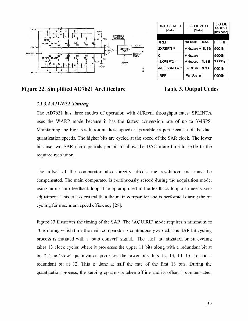
3.1.5.3 AD7621 Overview
The AD7621 is a 16 bit charge redistribution type ADC [6]. The action is the same as
described above but the input is differential, in this case. A simplified schematic of this
architecture is shown in figure 22. IN+ and IN- is the differential ADC input and can be
positive or negative. The reference voltage, REF, sets the full scale for the ADC. Two
identical capacitor DAC arrays are connected to the comparator inputs. The SAR
algorithm cycles through the 16-bits driving the comparator inputs towards balance. The
control logic handles the bit cycling and stores the digital output word. The output codes
are described in Table 3. The digital output 0000h corresponds to –REF and FFFFh
corresponds to +REF. The LSB is given by 162/2 REFV× . The reference value used in the
AD7621 as well as SPLINTA is 2.048V and the LSB = .5.622/048.22 16 uV=×
Figure 21. 3-bit Charge Redistribution Example
BIT CYCLING PROCESS; VIN=1.3, VREF=2 Start at time=t2
Set switch S1 to VREF
Vx=-VIN+VREF/2
= -1.3 + 2/2 = -0.3V
Is Vx < 0 ? Yes
Set Bit 1=1; Leave S1 set to VREF
At time= t3
Set switch S2 to VREF
Vx=-VIN+VREF/2+ VREF/4
= -1.2 + 2/2 +2/4= +0.2V
Is Vx < 0 ? No (Gray Level)
Set Bit 2=0; Switch S2 back to ground
At time= t4
Set switch S3 to VREF
Vx=-VIN+VREF/2+ VREF/8
= -1.2 + 2/2 +2/8= -0.05V
Is Vx < 0 ? Yes
Set Bit 3=1; Leave S3 set to VREF
0
1
2
-1
-2
time
Vx
SAMPLESAMPLE HOLD Bit 1 Bit 3 Bit 3
Conversion Start
Initiated Vx <0
Bit 1 =1
Vx >0
Bit 2 =0
Vx<0
Bit 3 =1
t1 t2 t3 t4 t5
Vx = 0
Vx = -1.3V
Vx = -0.3V
Vx = 0.2V
Vx = -.05
(residue)
0
1
2
-1
-2
time
Vx
SAMPLESAMPLE HOLD Bit 1 Bit 3 Bit 3
Conversion Start
Initiated Vx <0
Bit 1 =1
Vx >0
Bit 2 =0
Vx<0
Bit 3 =1
t1 t2 t3 t4 t5
Vx = 0
Vx = -1.3V
Vx = -0.3V
Vx = 0.2V
Vx = -.05
(residue)
39
3.1.5.4 AD7621 Timing
The AD7621 has three modes of operation with different throughput rates. SPLINTA
uses the WARP mode because it has the fastest conversion rate of up to 3MSPS.
Maintaining the high resolution at these speeds is possible in part because of the dual
quantization speeds. The higher bits are cycled at the speed of the SAR clock. The lower
bits use two SAR clock periods per bit to allow the DAC more time to settle to the
required resolution.
The offset of the comparator also directly affects the resolution and must be
compensated. The main comparator is continuously zeroed during the acquisition mode,
using an op amp feedback loop. The op amp used in the feedback loop also needs zero
adjustment. This is less critical than the main comparator and is performed during the bit
cycling for maximum speed efficiency [29].
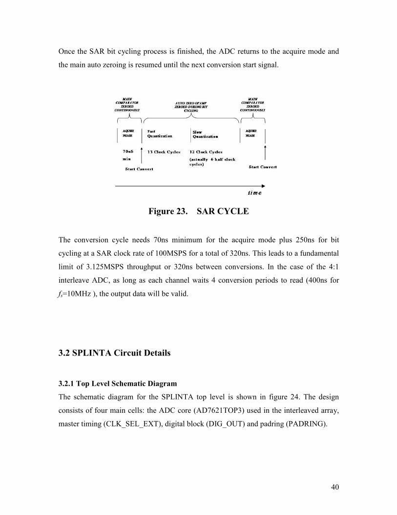
Figure 23 illustrates the timing of the SAR. The ‘AQUIRE’ mode requires a minimum of
70ns during which time the main comparator is continuously zeroed. The SAR bit cycling
process is initiated with a ‘start convert’ signal. The ‘fast’ quantization or bit cycling
takes 13 clock cycles where it processes the upper 11 bits along with a redundant bit at
bit 7. The ‘slow’ quantization processes the lower bits, bits 12, 13, 14, 15, 16 and a
redundant bit at 12. This is done at half the rate of the first 13 bits. During the
quantization process, the zeroing op amp is taken offline and its offset is compensated.
Figure 22. Simplified AD7621 Architecture Table 3. Output Codes
DIGITAL
OUTPUT
[hex code]
DIGITAL VALUE
[Volts]
ANALOG INPUT
[Volts]
FFFFhFull Scale – 1LSB+REF
8001hMidscale + 1LSB2XREF/216
8000hMidscale0
7FFFhMidscale - 1LSB-2XREF/216
0001h-Full Scale + 1LSB-REF+ 2XREF/216
0000h-Full Scale-REF
DIGITAL
OUTPUT
[hex code]
DIGITAL VALUE
[Volts]
ANALOG INPUT
[Volts]
FFFFhFull Scale – 1LSB+REF
8001hMidscale + 1LSB2XREF/216
8000hMidscale0
7FFFhMidscale - 1LSB-2XREF/216
0001h-Full Scale + 1LSB-REF+ 2XREF/216
0000h-Full Scale-REF
40
Once the SAR bit cycling process is finished, the ADC returns to the acquire mode and
the main auto zeroing is resumed until the next conversion start signal.
The conversion cycle needs 70ns minimum for the acquire mode plus 250ns for bit
cycling at a SAR clock rate of 100MSPS for a total of 320ns. This leads to a fundamental
limit of 3.125MSPS throughput or 320ns between conversions. In the case of the 4:1
interleave ADC, as long as each channel waits 4 conversion periods to read (400ns for
fs=10MHz ), the output data will be valid.
3.2 SPLINTA Circuit Details
3.2.1 Top Level Schematic Diagram
The schematic diagram for the SPLINTA top level is shown in figure 24. The design
consists of four main cells: the ADC core (AD7621TOP3) used in the interleaved array,
master timing (CLK_SEL_EXT), digital block (DIG_OUT) and padring (PADRING).
Figure 23. SAR CYCLE

41
The strategy for the design of this system was to reuse existing cells wherever possible.
Reusing existing circuits lessens the risks associated with the individual designs and
shifts the focus to system level issues specific to SPLINTA. The ADC core, master
timing cell, and ESD cells contained in the padring, are all reused from existing circuits.
Please refer to [3, 6, 29, 31] for detailed coverage of these design specifics. The circuit
details presented here describe the system level design of SPLINTA and the pertinent
circuits to support it.
Figure 26. SPLINTA Top Level Schematic Diagram
Figure 24. SPLINTA Top Level Schematic Diagram

42
3.2.1.1 System Noise Issues
Digital noise is a serious concern in mixed signal circuits such as SPLINTA (see section
4.3). Several precautions are taken to isolate the cells and minimize the noise while
balancing practical considerations for the physical size and packaging.
The external reference is brought in separately to each converter. Since eight of the nine
capacitor DACs are operational at any given time, quite a bit of noise is generated on the
reference line. If they are not separated, one converter can be subjected to large noise
transients on the reference by direct coupling from another converter. This can lead to
crosstalk between converters, compromising the ADC performance. This effect is
described in more detail in Chapter 4.
In addition to separating the reference lines, there are several power supply and ground
pins on SPLINTA. Isolation is important between supplies also, but not as critical as with
the ADC reference. Considerations such as substrate noise and ground bounce [30] are a
concern for power supply lines in mixed-signal circuits and it is common practice to
separate analog and digital supplies to minimize coupling of this noise from the digital
into the analog circuits. SPLINTA further separates the analog and digital supplies,
trading off package constraints with noise concerns. There are 16 pins available for the
supplies in the present 100 pin package and are partitioned as 3 pair for analog, 3 pair for
output digital driver and 2 pair for ‘internal’ digital supplies. The decision for this power
supply scheme is based on the fact that the internal logic requires less current than the
analog or output driver cells and can be managed with one less supply.
The grouping of the cells for the supply pins is based on physical proximity of the cells to
the package pins. The ADC array is separated into groups of three for the analog and
digital output driver supplies. The three digital output driver supplies also power the two
16-bit digital output drivers, DOUTA and DOUTB, and the ‘ADC TAG’ and ‘BUSY’
lines. Ideally, 3 supplies for the internal digital circuits would be better to maintain the
grouping; unfortunately there are only 4 pins available. In an effort to balance the two
43
available supplies, cells are split into two groups of 4 converters and 3 converters plus the
digital block. The exact pinout and routing is explained in more detail in Chapter 5.
3.2.2 ADC Array
The ADC array uses a modified version of the Analog Devices AD7621 [6] architecture
for the core. The performance of this circuit is well known and the goal of SPLINTA is to
replicate this performance at 4 times the frequency. This was chosen because of its high
resolution and relatively high speed. It is a charge redistribution SAR type ADC (sec
3.1.5) which operates from a single 2.5V supply [6]. Figure 25 shows the AD7621 block
diagram highlighting the main differences between it and the SPLINTA ADC. The
SPLINTA core uses an external reference and does not need the internal reference. Also
the ADC internal timing is modified to accommodate the master timing signals (sec
3.1.4). The new internal timing cell is reused from an ADI 4:1 interleaved project chip
[31] which uses the same timing scheme as well as the AD7621 as the core ADC. That
work uses a more traditional 4 ADC approach and is still under evaluation.
Figure 25. AD7621 based ADC core

44
The ADC array is designed to have common connections where possible to save on the
pin count without compromising good isolation. The nine ADCs share the differential
input lines. They also share the digital control and calibration lines which are used only
during the initial linearity calibration (appendix A), otherwise they remain fixed. The
selection of the conversion start pulses for each ADC is handled in the digital section, as
are the chip select lines, CSB, used for the linearity calibration. The ADC individual
digital outputs are routed separately to the digital section for processing. The reference
and power supply connections are separated for maximum isolation, minimum noise and
practical considerations (sec 3.2.1.1).
3.2.3 SPINTA Master Timing Cell
To minimize timing errors, a single external master clock drives the timing circuits for all
ADC in the array. The timing for SPLINTA is generated from an external clock and is
common to all 9 ADCs to minimize timing mismatches (sec 3.1.4). This required
modifications to the AD7621s internal timing logic (sec. 3.2.2) and the addition of a
‘master’ timing cell at the top level (CLK_EXT_SEL in figure 24). The diagram for the
master timing cell is shown in figure 26. The TIMING PULSE GENERATOR was
reused from the ADI project chip, as mentioned above.
The external SAR clock is processed by the TIMING PULSE GENERATOR, to provide
the six timing signals that control the SAR cycles. The op-amp offset zeroing function
(sec 3.1.5) uses four controls, OZ, OZQ, OZS, and OZQS. Each of the six timing signals
is connected to the 9X BUFFER blocks and routed separately to each of the ADCs for a
total of 54 timing signals. The D type flip-flop is used to synchronize the external SYNC
pulse with the master clock (sec 3.1.3) to provide the conversion start signal,
CNVSTBIN.

45
3.2.4 Digital Block
The digital block, DIG_OUT, is the only ‘new’ circuit on SPLINTA. The schematic is
shown in figure 27. It contains the logic for the interleaving multiplexer arrays which
assemble the individual ADC outputs into the high speed A and B outputs. It also
contains the de-multiplexer that handles the routing of the conversion start pulses. The
routing for the CSB input and BUSY outputs, used for the linearity calibration, is also
contained here.
The DATA OUTPUT MUX routes each bit from each ADC into 16 8:1 multiplexer
arrays, one for each bit. The READA and READB busses are a shifted version of the
SELA and SELB lines (sec 3.1.3) and select which of the ADC 16-bit words will be
routed to which of the A or B outputs. The outputs are buffered then routed to the
padring. The READA and READB busses are also buffered and routed to the padring to
be used as the ADC tags to identify which ADC the data came from.
MASTER
CLOCK
TIMING PULSE
GENERATOR
(reused)
MASTER
CLOCK
MASTER OZ
MASTER
LATCH
D
CK
Q
SYNC
9X
BUFFER
4 9X
BUFFER
9X
BUFFER
9X
BUFFER
9X
BUFFER
TO ADC
ARRAY
CNVSTBIN
9X
BUFFER
MASTER
CLOCK
TIMING PULSE
GENERATOR
(reused)
MASTER
CLOCK
MASTER OZ
MASTER
LATCH
D
CK
Q
SYNC
9X
BUFFER
4 9X
BUFFER
9X
BUFFER
9X
BUFFER
9X
BUFFER
TO ADC
ARRAY
CNVSTBIN
9X
BUFFER
Figure 26. Master Timing Block

46
The CSB de-multiplexer is used during the linearity calibration. The TEST[0:1] pins
actives the de-multiplexer and the selection line for channel A determines which ADC is
to be calibrated. The CSB control signal is routed to the ADC to be calibrated according
to the SELA bus. ‘BUSY’ lines from each ADC are multiplexed to the two BUSYA and
BUSYB outputs within this block. They are used when evaluating a single ADC within
the array or during the linearity calibration. They can also be used to signal when data is
valid (sec 3.1.3).
Figure 27. SPLINTA Digital Block
3.2.5 Padring
The schematic diagram for the padring is shown in figure 28. As mentioned before, the
ESD cells are reused from the AD7621 and the AD interleaved project chip [31]. The
strategy here was to use the existing interleaved structure as a guide for the best
arrangement.

47
The ESD protection circuits, ESDSUPPLY_2P5, are used to protect the reference, analog
supply and internal digital supply pins. ESDSUPPLY_3P3 are used for the output driver
supplies because they use higher voltage devices. ESD clamps are used to protect the
many (13) VSS pins. The supplies for the digital outputs are organized depending on
which driver supply it is associated with. Chapter 5 details the power supply strategy.
Figure 28. PADRING

48
4 Simulation Results
In large systems such as SPLINTA, convergence for a complete transistor level model
simulation is difficult, if at all possible. Even when convergence is achieved, the transient
analysis times are prohibitively long. For this reason, simulations for SPLINTA were
done mostly at a high behavioral level. The behavioral simulations results were ‘spot’
checked with transistor level models used on the analog portions of the ADCs as well as
the ESD cells in the padring.
Three types of simulations were performed to verify the SPLINTA design. Although the
target sampling rate for SPLINTA is 10MSPS, these simulations were performed at 12
MSPS. Functional simulations are done both at the behavioral level and transistor level to
verify operation. The models used are for a 0.25u CMOS process. Some simulations were
performed with package parasitic modeling on the reference pins. Simulations with the
package parasitic were performed at the transistor level for the analog sections. Lastly,
simulations are done specifically to be used with the MATLAB correction algorithm to
demonstrate the calibration results.
4.1 Simulation Test Circuit
The basic test circuit used for these simulations is shown in figure 29. The power source
is a single 2.5V supply. The external reference is 2.048V and the differential input can
span the +/- 2.048 range. The sampling rate is 12MHz and the master timing or SAR
clock is set at 96MHZ.

49
Ideal voltage sources are used to supply power and the reference voltage. The control
lines are hard wire for normal operation (refer to Table 7 in Chapter 5 for pin
functionality). The input voltage is applied differentially also using ideal voltage sources.
Behavioral models for test DACs are used to convert ADC outputs back to analog voltage
levels for analysis purposes. The ‘Data Logger’ is also a behavioral model that records
the ADC outputs in a text file to be used with the MATLAB correction algorithm.
Figure 29. Simulation Test Circuit
4.2 Functional Simulations
This simulation was the baseline used for functionality verification. The differential input
is set to ramp up N number of bits around any value within +/- full scale range at a rate of
1LSB/Conversion Rate: 62.5uV/83.33uS. The selection lines are configured to randomly
cycle through ADC pairs as described in sec 2.3.1.
Figure 30 shows waveforms for a section of approximately 10 bits at mid-scale for a
typical SPLINTA simulation run. The differential input is set around zero and is ramped
DATA LOGGER
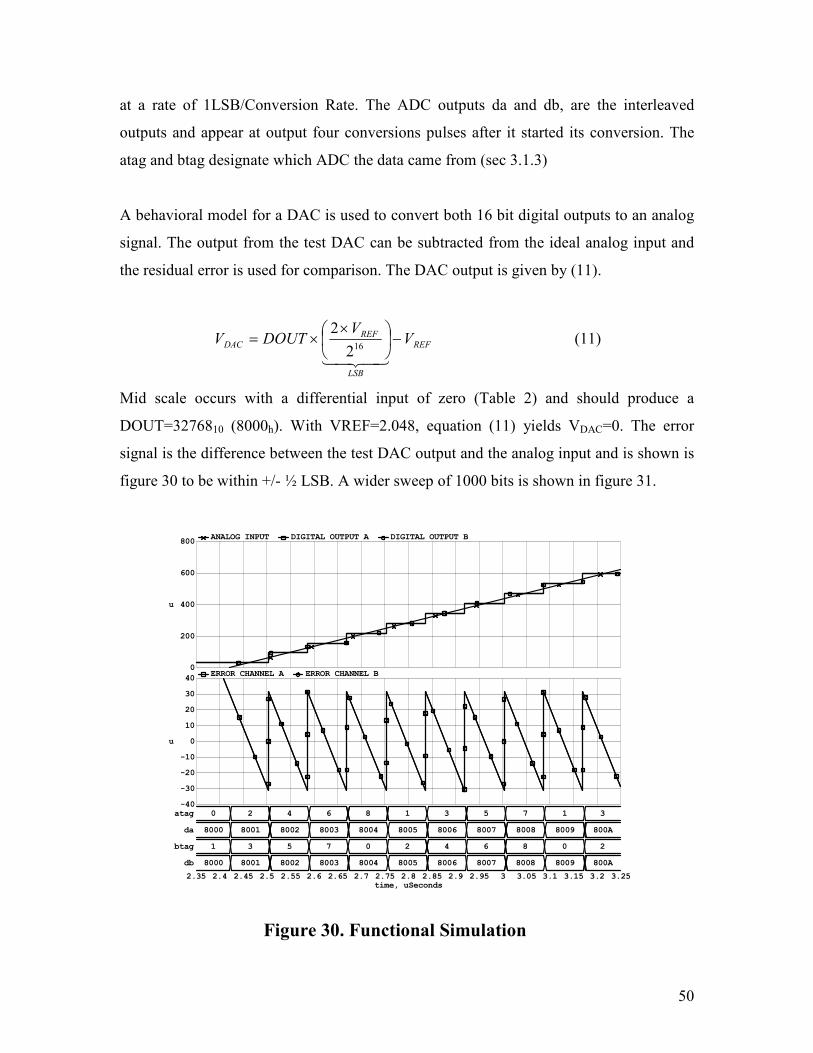
50
at a rate of 1LSB/Conversion Rate. The ADC outputs da and db, are the interleaved
outputs and appear at output four conversions pulses after it started its conversion. The
atag and btag designate which ADC the data came from (sec 3.1.3)
A behavioral model for a DAC is used to convert both 16 bit digital outputs to an analog
signal. The output from the test DAC can be subtracted from the ideal analog input and
the residual error is used for comparison. The DAC output is given by (11).
REF
LSB
REFDAC V
VDOUTV −
××=
43421162
2 (11)
Mid scale occurs with a differential input of zero (Table 2) and should produce a
DOUT=3276810 (8000h). With VREF=2.048, equation (11) yields VDAC=0. The error
signal is the difference between the test DAC output and the analog input and is shown is
figure 30 to be within +/- ½ LSB. A wider sweep of 1000 bits is shown in figure 31.
ANALOG INPUT DIGITAL OUTPUT A DIGITAL OUTPUT B
0
200
400
600
800
u
ERROR CHANNEL A ERROR CHANNEL B
-40
-30
-20
-10
0
10
20
30
40
u
atag 0 2 4 6 8 1 3 5 7 1 3
da 8000 8001 8002 8003 8004 8005 8006 8007 8008 8009 800A
btag 1 3 5 7 0 2 4 6 8 0 2
db 8000 8001 8002 8003 8004 8005 8006 8007 8008 8009 800A
2.35 2.4 2.45 2.5 2.55 2.6 2.65 2.7 2.75 2.8 2.85 2.9 2.95 3 3.05 3.1 3.15 3.2 3.25time, uSeconds
Figure 30. Functional Simulation

51
This simulation provides a baseline for the functionality verification. This was the
standard test repeated with transistor level models and at both + and – full scale to verify
functionality each time a change was made to the circuit.
4.3 Transistor Level Simulations with Bond Wire Parasitics
Noise coupling through package parasitics is a major concern in mixed signal integrated
circuits [32]. This is especially a concern for interleaved ADCs such as SPLINTA where
quite a bit of digital noise is generated from multiple converters working simultaneously.
Digital noise can be coupled to the analog circuits through substrate and common
connections such as supplies and references compromising performance. These issues are
addressed by careful layout and package pin arrangement. Ideally circuits should be
simulated at the transistor level, with parasitics included, to uncover problems before
fabrication. This is very difficult and time consuming, if possible at all, due to the
complexity at this level. In general, a combination of simulation and careful layout is
relied on for best results.
Figure 31. Functional Simulation-1000 bits

52
Simulations to investigate package parasitic effects were performed on SPLINTA with
limited success. Convergence for circuits including power supply parasitics proved nearly
impossible. However, simulations with package parasitics on the ADC reference
uncovered a potentially serious flaw in the original pinning strategy. Initially, one
common pin was used to connect the external reference to all nine ADCs. The
simulations showed that using common reference pins results in noise generated from one
ADC affecting the conversion results of another, commonly known as crosstalk.
4.3.1 Transistor Level Simulation
Since an all transistor level simulation is nearly impossible, a compromise is made where
the analog portions of the ADCs are modeled at the transistor level and the digital
portions are modeled at the behavioral level. The partitioning for the ADC core is shown
in Figure 34. The padring (not shown), which contains all the ESD protection is also
modeled at the transistor level. Simulations showed that this level of modeling is
sufficient to see parasitic effects.
Transistor Level
Modeling
Behavioral
Modeling
Figure 32. Modeling Level for SPLINTA ADC
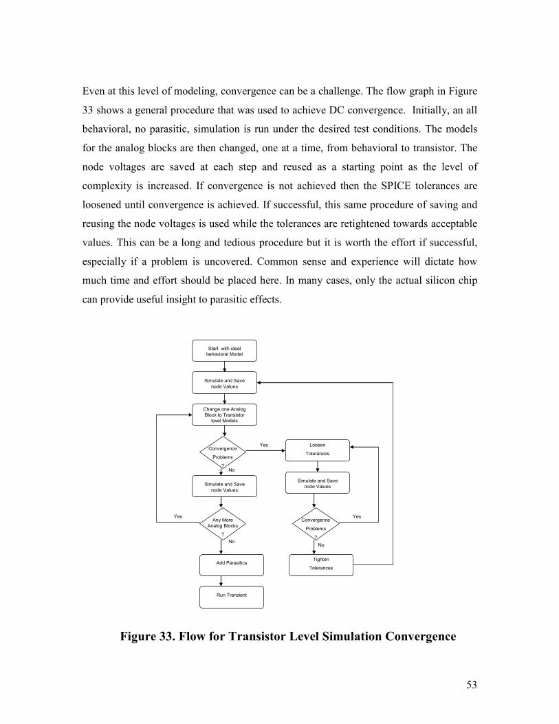
53
Even at this level of modeling, convergence can be a challenge. The flow graph in Figure
33 shows a general procedure that was used to achieve DC convergence. Initially, an all
behavioral, no parasitic, simulation is run under the desired test conditions. The models
for the analog blocks are then changed, one at a time, from behavioral to transistor. The
node voltages are saved at each step and reused as a starting point as the level of
complexity is increased. If convergence is not achieved then the SPICE tolerances are
loosened until convergence is achieved. If successful, this same procedure of saving and
reusing the node voltages is used while the tolerances are retightened towards acceptable
values. This can be a long and tedious procedure but it is worth the effort if successful,
especially if a problem is uncovered. Common sense and experience will dictate how
much time and effort should be placed here. In many cases, only the actual silicon chip
can provide useful insight to parasitic effects.
Start with ideal
behavioral Model
Simulate and Save
node Values
Change one Analog
Block to Transistor
level Models
Convergence
Problems
?
Loosen
Tolerances
Simulate and Save
node Values
Convergence
Problems
?
Tighten
Tolerances
Yes
Yes
No
No
Simulate and Save
node Values
Any More
Analog Blocks
?
No
Yes
Add Parasitics
Run Transient
Figure 33. Flow for Transistor Level Simulation Convergence
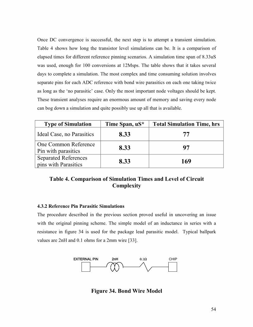
54
Once DC convergence is successful, the next step is to attempt a transient simulation.
Table 4 shows how long the transistor level simulations can be. It is a comparison of
elapsed times for different reference pinning scenarios. A simulation time span of 8.33uS
was used, enough for 100 conversions at 12Msps. The table shows that it takes several
days to complete a simulation. The most complex and time consuming solution involves
separate pins for each ADC reference with bond wire parasitics on each one taking twice
as long as the ‘no parasitic’ case. Only the most important node voltages should be kept.
These transient analyses require an enormous amount of memory and saving every node
can bog down a simulation and quite possibly use up all that is available.
Type of Simulation Time Span, uS* Total Simulation Time, hrs
Ideal Case, no Parasitics 8.33 77
One Common Reference
Pin with parasitics 8.33 97
Separated References
pins with Parasitics 8.33 169
4.3.2 Reference Pin Parasitic Simulations
The procedure described in the previous section proved useful in uncovering an issue
with the original pinning scheme. The simple model of an inductance in series with a
resistance in figure 34 is used for the package lead parasitic model. Typical ballpark
values are 2nH and 0.1 ohms for a 2mm wire [33].
CHIP 2nH 0.1ΩEXTERNAL PIN CHIP 2nH 0.1ΩEXTERNAL PIN
Figure 34. Bond Wire Model
Table 4. Comparison of Simulation Times and Level of Circuit
Complexity

55
This model was placed in series with the reference package pin. The original 80-pin
design is shown in figure 37. The ADCs shared one common reference pin connected to
an external source. The simulation test circuit is the same as described in section 4.2. The
input in ramped up at 1LSB/conversion time around mid scale.
A baseline was established by running a transistor level simulation without parasitics, this
is shown in 36a. The waveforms in figure 36b show the effects of the noisy reference.
The addition of the parasitic model causes large noise transients on the reference line
from the cap DACs. The worse transients are when the MSB is cycled (section 3.1.3) and
occurs at a rate of fsample. These periodic perturbations from one ADC can cause bit errors
on another ADC, particularly if it is at the end of its bit cycling making decisions on the
LSBs.
Figure 35. Original 80-pin SPLINTA Design

56
Ideally, the error in the ADC transfer function should be between +/- ½ LSB as in the
baseline plot in 36a. The parasitic plot in 36b shows the converter regularly getting
‘stuck’ for 4 conversions. The noise generated from this pinning strategy clearly
compromises the ADC resolution with errors of +/- 2 LSBs.
The package diagram in figure 35 shows that some of the package pins were not used.
There were enough ‘spare’ pins to be able to separate the references into groups of 3 and
still remain in the smaller package. A simulation was done for this case to determine if
this level of isolation was sufficient. Figure 37 shows the results of this case. This
arrangement improved the problem somewhat but still made the occasional mistake when
one ADC was making an MSB decision while another ADC from the same group was
making LSB decisions. This strategy not only had bit errors but channels A and B could
be different from one another. It was evident from these results that any excessive noise
generated from one ADC was likely to corrupt another ADC output when they are
sharing a common reference.
Figure 36. Simulations on Original 80-pin SPLINTA Design
with and without Parasitics
a. Baseline
b. With Parasitics
b. With Parasitics
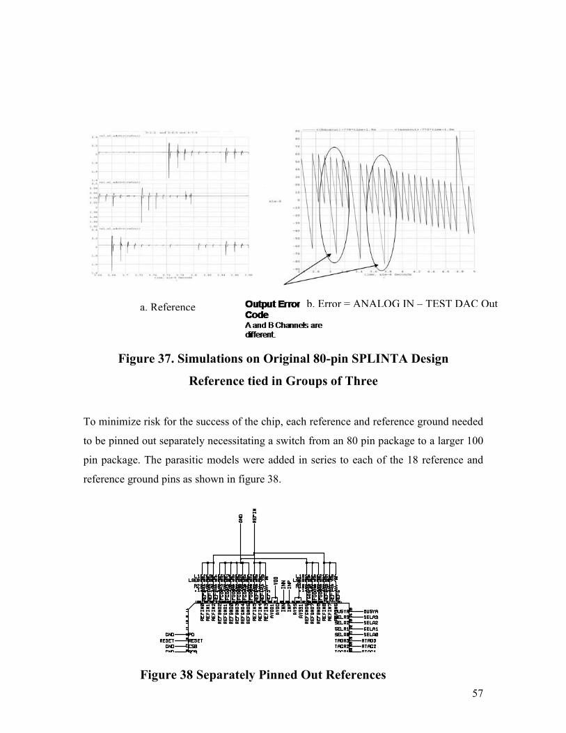
57
To minimize risk for the success of the chip, each reference and reference ground needed
to be pinned out separately necessitating a switch from an 80 pin package to a larger 100
pin package. The parasitic models were added in series to each of the 18 reference and
reference ground pins as shown in figure 38.
Figure 37. Simulations on Original 80-pin SPLINTA Design
Reference tied in Groups of Three
b. Error = ANALOG IN – TEST DAC Out
Figure 38 Separately Pinned Out References
a. Reference

58
A new baseline simulation was run with this new pinout as well as another parasitic run
with one common reference, for comparison purposes. The analog input for these
simulations is ramped at a rate slightly faster than 1 bit/conversion as used previously
which is the reason it looks slightly different than the previous simulations. Figure 39
shows a snapshot of this ramp along with the digitized version from the test DAC. The
top trace (1) has all the references tied to one common reference pin through parasitics.
The test DAC output gets routinely ‘stuck’ for four LSBs reducing the resolution from
16-bits to 14-bits. Trace (2) shows the output with the references tied separately through
the parasitics. These results are identical to the baseline results in (3), without parasitics,
verifying that this level of isolation is essential to maintain high resolution for this type of
architecture.
4.3.3 Issues with Supply Pin Parasitic Simulations
As the previous section demonstrated, there is no doubt that simulations of this type are
invaluable to successful circuit design. Uncovering problems such as this before chip
fabrication saves much time, money and aggravation. However, the closer the models are
Comparison of 3 cases : 2:Common Reference with Parasitics 3:Separate Reference with parasitics
1:No Parasitics
Error - common reference with parasitic
-150
-100
-50
0
50
100
150
200
u
Error - separate references with parasitics
-75
-50
-25
0
25
50
75
u
Error - no parasitics
-75
-50
-25
0
25
50
75
u
2.6 3 3.4 3.8 4.2 4.6 5 5.4 5.8 6.2 6.6 7 7.4 7.8 8.2
time, uSeconds
Comparison of 3 cases : 2:Common Reference with Parasitics 3:Separate Reference with parasitics
1:No Parasitics
Test Dac Output - common reference with parasitic Analog Input
.2
.4
.6
.8
1
1.2
m
2:<>v(da) 7FFD 8000 8001 8004 8005 80092:<>v(db) 7FFD 8000 8001 8004 8005 8009
Test DAC Output - separate references with parasitics Analog Input
.2
.4
.6
.8
1
1.2
m
3:<>v(da) 7FFD 7FFE 8000 8001 8002 8004 8005 8006 8007 8009 800A 800B3:<>v(db) 7FFD 7FFE 8000 8001 8002 8004 8005 8006 8007 8009 800A 800B
Test DAC output - no parasitics Analog Input
.2
.4
.6
.8
1
1.2
m
1:<>v(da) 7FFD 7FFE 8000 8001 8002 8004 8005 8006 8007 8009 800A 800B1:<>v(db) 7FFD 7FFE 8000 8001 8002 8004 8005 8006 8007 8009 800A 800B
5.35 5.45 5.55 5.65 5.75 5.85 5.95 6.05 6.15 6.25 6.35
time, uSeconds
(1) Common
Reference
through
Parasitics
(2) References
Tied Separately
through
Parasitics
(3) No Parasitics
A. Analog input and Test DAC output B. Error between Analog input and Test
DAC output
Figure 39. 100-pin Package Simulation Results
59
to reality, i.e. transistor level models with chip and package parasitics, the greater the
difficulty achieving DC convergence. Even if successful, it doesn’t necessarily guarantee
a successful transient analysis. In some cases the transient simulation can run for hours or
days until a certain point and get ‘stuck’. This is most likely to occur when several things
are switching at once.
This was precisely the case with a transient analysis attempted with bond wire parasitics
on the analog power supply pins. The simulation gets stuck at the beginning of first
conversion cycle and can’t resolve the transitions. Several attempts where made to get
past the ‘stuck’ point, such as, loosening the tolerances and reducing the level of
complexity by modeling some analog portions at the behavioral level, and forcing
SPLINTA to a known state past the ‘stuck’ point. None of these attempts were
successful.
It is not always practical or even possible, as in this case, to cover every scenario in
simulation and careful layout and pin strategy is the best and sometimes only practical
solution. Chapter 5 describes the physical layout and pin arrangement. The goal is to
isolate as best as possible. The PSRR of the comparator should alleviate some of the
supply coupling so it should not be as dramatic as the reference problem [29].
4.4 Matlab Correction Algorithm
The MATLAB correction algorithm was developed at Worcester Polytechnic Institute
[5]. It is a mathematical model for the algorithm described in section 2.3.2 and is the
basis for the hardware implementation being developed at WPI concurrently with this
project. The block diagram in figure 40 is the model used to demonstrate the complete
self-calibrating ADC system. In the absence of hardware, the MATLAB code can be
used to verify the correction algorithm on SPLINTA simulation data.
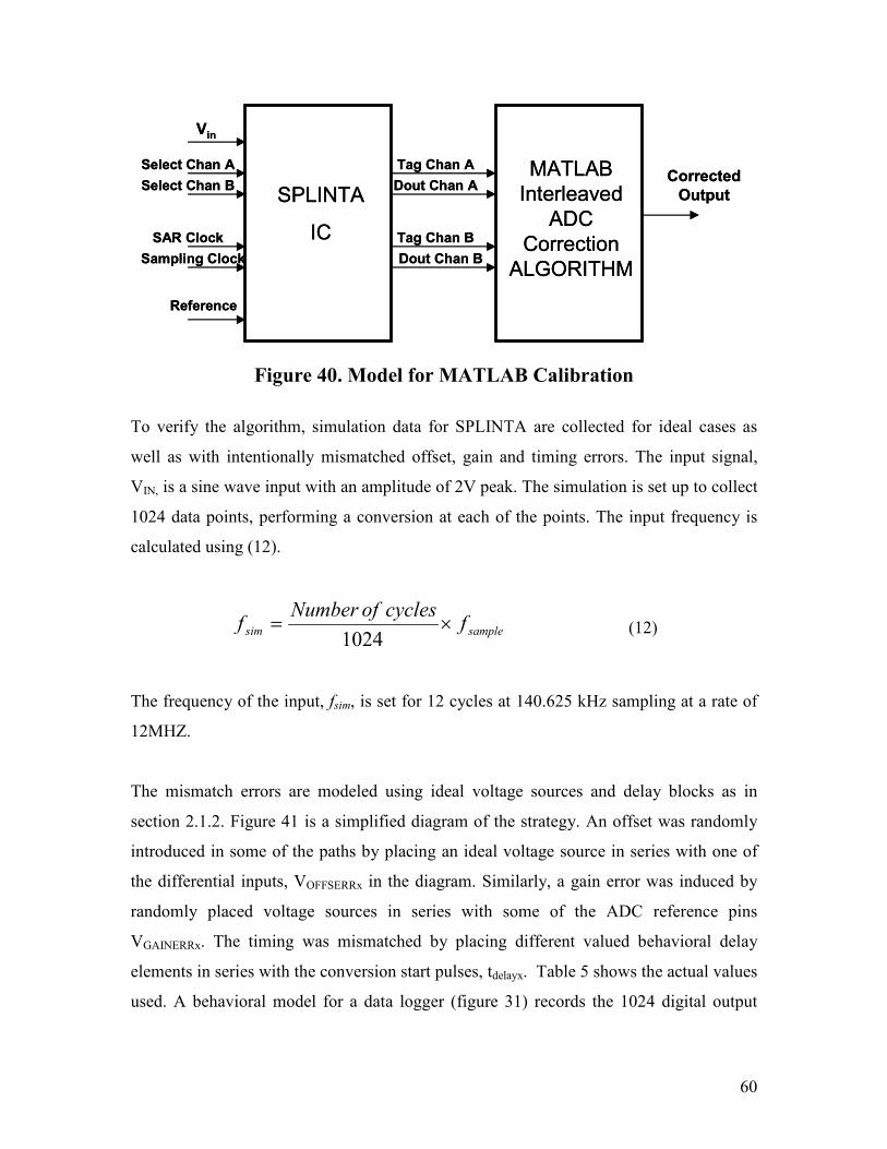
60
SPLINTA
IC
MATLAB
Interleaved
ADC
Correction
ALGORITHM
Vin
Select Chan A
Select Chan B
SAR Clock
Sampling Clock
Reference
Tag Chan A
Dout Chan A
Dout Chan B
Tag Chan B
Corrected
OutputSPLINTA
IC
MATLAB
Interleaved
ADC
Correction
ALGORITHM
Vin
Select Chan A
Select Chan B
SAR Clock
Sampling Clock
Reference
Tag Chan A
Dout Chan A
Dout Chan B
Tag Chan B
Corrected
Output
Figure 40. Model for MATLAB Calibration
To verify the algorithm, simulation data for SPLINTA are collected for ideal cases as
well as with intentionally mismatched offset, gain and timing errors. The input signal,
VIN, is a sine wave input with an amplitude of 2V peak. The simulation is set up to collect
1024 data points, performing a conversion at each of the points. The input frequency is
calculated using (12).
samplesim fcyclesofNumber
f ×=1024
(12)
The frequency of the input, fsim, is set for 12 cycles at 140.625 kHz sampling at a rate of
12MHZ.
The mismatch errors are modeled using ideal voltage sources and delay blocks as in
section 2.1.2. Figure 41 is a simplified diagram of the strategy. An offset was randomly
introduced in some of the paths by placing an ideal voltage source in series with one of
the differential inputs, VOFFSERRx in the diagram. Similarly, a gain error was induced by
randomly placed voltage sources in series with some of the ADC reference pins
VGAINERRx. The timing was mismatched by placing different valued behavioral delay
elements in series with the conversion start pulses, tdelayx. Table 5 shows the actual values
used. A behavioral model for a data logger (figure 31) records the 1024 digital output

61
data points and tags for channels A and B into a text file that can be imported into
MATLAB.
The MATLAB algorithm is designed to compute the errors between each ADC pair
combination and apply that estimate each time that pair is selected (sec 2.3.2). In general,
the correction algorithm needs 200K+ points for initial convergence. It is not practical to
ADC0
ADC1
ADC8SIG IN
SEL ADC A
MASTER
CLOCK
SYNC
100MHz
Timing
Logic
SAR TIMING
10MHz
MUX
READ B
DIGITAL
OUTPUT
BLOCKS
CNVST
DOUT
DOUTCNVST DOUTB
DOUTA
TAGB
BUSYB
SEL ADC B
TAGA
REFERENCE
READ A
CNVST
BUSYA/B
CNVSTDOUT
BUSYA/B
BUSYA/B
BUSYA
VGAINERR0
VGAINERR1
VGAINERR8
VOFFSERR0
VOFFSERR1
VOFFSERR8
tdelay0
tdelay1
tdelay8
tdelay
ps
VGAINERR
mV
VOFFSERR
mVADC
0008
40007
0006
15055
25-504
10063
65-102
01041
50-3100
Error Values for Interleave Errors
tdelay
ps
VGAINERR
mV
VOFFSERR
mVADC
0008
40007
0006
15055
25-504
10063
65-102
01041
50-3100
Error Values for Interleave Errors
Figure 41. Block Diagram for Interleave Simulation
with Mismatch Errors
Table 5 Induced Error Values

62
directly collect this amount of data from simulation. The simulation time would be
prohibitively long (sec 4.3). For this reason, only 1024 points are collected for the FFT
and a compromise is made by replicating the data 500 times for a total of 512K data
points.
An FFT of the MATLAB results is shown Figure 42. The spectrum for the ‘ideal’
simulation data shows a noise floor of around -130db. The spectrum from the simulation
corrupted with the mismatch errors shows the noise floor at around -80dB. The mismatch
errors do not cause spurs in the spectrum because of the decorrelation of the errors by the
randomization of the ADC selection (sec 2.1.3). This data is processed by the MATLAB
algorithm for correction. The calibration completely removes the effects of the error. The
data output has a noise floor as good as the ‘error free’ data.
Figure 43 shows a MATLAB plot of convergence of the algorithm. The error settles to
within 1 LSB in 200K conversions. For an fsample of 10MHZ, the convergence time is
20ms.
Simulation Data no errors
Simulation Data with induced errors
Corrected Data
Figure 42. MATLAB Calibration Results

63
Figure 43. MATLAB Convergence

64
5 Physical Layout and Packaging
The technology used in the SPLINTA design is a 0.25u CMOS process with 5 metal
layers. The physical design and package selection balances maximum isolation and
matching with practical size limitations.
5.1 Physical Layout
The physical layout of SPLINTA is as critical as the simulation verification (section 4).
Figure 44 is a plot of the physical layout. Even though the calibration algorithm (sec
2.3.2) is designed to correct for any mismatches in the channel, care still needs to be
taken to keep the blocks as well matched and as isolated as possible for optimal
performance. Identical ADC layouts are surrounded by guard rings and arranged in a 3 X
3 grid. Placement of the digital block is not critical but the timing block is placed close to
ADC0 to minimize the routing to the timing calibration. ADC0 is the only cell used to
calibrate the master timing block.
The offset and timing errors can be affected by the input signal paths. To ensure the best
possible matching, routing for the differential input lines are intentionally shaped so that
the lengths and area are the same. All of the differential path lengths to the nine ADCs
are matched to the longest path in the array. These lines are also shielded to provide some
isolation.

65
The length of the reference lines is not as critical as far as timing is concern. However
they are designed to be as wide as possible for a low impedance path to the pad. The pads
are located around the chip such that the paths are short, further minimizing the
impedance. They are also shielded to provide some added isolation.
To prevent the digital noise from interfering with analog supplies, the supply pins are
separated into three types: analog, internal digital and output driver supplies (sec.
3.2.1.1). Because of the large amount of switching and digital activity, these types are
further separated into subgroups to minimize crosstalk and supply bounce [30]. The
analog and output driver supplies are separated into groups of three and the digital supply
into groups of two (sec 5.2). In addition, each power and ground pin from each core ADC
is Kelvin connected back to its supply pin.
The size of this layout is approximately 7mm X 7mm and will fit in a 100 pin LQFP
package.
Figure 44. SPLINTA LAYOUT

66
5.2 Pad Layout
Figure 45 shows the chip pad arrangement and the bonding. The total number of pads on
the chip totals 108. Given the die size and number of pins a 100-pin LQFP package with
a 9000um2 cavity size is chosen for packaging. Some of the supplies and grounds will
share a pin to fit in the 100-pin package. To minimize the parasitic impedance, the analog
and supply pads are arranged around the chip so that they are physically close to the cells
they connect to.
Ideally, for maximum isolation, each block in the system would have its own analog,
digital and output driver supply pins. Due to the limited number of pins, compromises are
made by double bonding and evenly distributing all of the available pins for power
between the cells.
There are six pairs of analog supply pads on the chip. Each ADC cell has the comparator
supply separated from the timing supply and routed to its own pad. They will be double
bonded to the same package pin. The analog pins are AVDDA/B/C and AVSSA/B/C.
The digital output drivers can have very large switching transients, particularly with two
sets of digital data outputs switching simultaneously. These supplies are also grouped in
sets of three: OVDDA/B/C, OVSSA/B/C.
Unfortunately, there is room only for two more pairs of supply pins, the internal digital:
DVDDA/B, DVSSA/B. The substrate connections are split into two groups, SAGNDA
and SAGNDB, routed to a separate chip pad, and then double bonded with the DVSSA
and DVSSB pins. This arrangement is a compromise and was chosen because the digital
supply pins for the internal logic do not have as high current level as the other groups.
All supply pins are located on the chip to be as close to the blocks they power as possible.
Table 6 lists the supply pads and the cell groupings that connect to them.
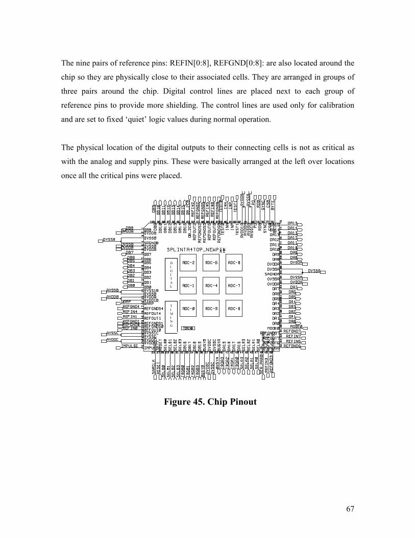
67
The nine pairs of reference pins: REFIN[0:8], REFGND[0:8]: are also located around the
chip so they are physically close to their associated cells. They are arranged in groups of
three pairs around the chip. Digital control lines are placed next to each group of
reference pins to provide more shielding. The control lines are used only for calibration
and are set to fixed ‘quiet’ logic values during normal operation.
The physical location of the digital outputs to their connecting cells is not as critical as
with the analog and supply pins. These were basically arranged at the left over locations
once all the critical pins were placed.
Figure 45. Chip Pinout
D
I
G
I
T
A
L
T
I
M
IN
G

68
5.3 Power Supply Partitioning
5.3.1 Analog Supplies
The ADCs are separated into to groups of three to minimize crosstalk through the supply
pins: VDDA/B/C and VSSA/B/C (Table 6). Figure 45 shows the chip pad arrangement.
The supplies for the timing block of each ADC are separated from the main analog
supply. VDD1A/B/C and VSS1A/B/C are grouped in the same fashion as the main
analog supply and routed to their own pad on the chip. Since there is a shortage of pins
on the package, these will be bonded to the same pin as their main analog supply
counterpart. This strategy is modeled after an existing interleaved SAR based project chip
[31].
The master timing block for this chip is at the top level, common to all ADC’s. The
calibration and the test modes for this cell are controlled by ADC0; therefore it is
powered by the same timing supply: VDD1C, VSS1C.
5.3.2 Output Driver Supplies
The output driver supplies power the internal ADC ROMs as well as the output digital
drivers. These are also separated into groups of three to minimize ground bounce [30]:
OVDDA/B/C, OVSSA/B/C. The internal ROM power is grouped the same way as the
SPLINTA SUPPLY PADS 2/22/2007
Name Function Notes
DVDDA, DVSSA Power and Gnd for Internal Digital Connection for internal digital for ADC1, 2, 5, 4, 8
SAGNDASubstrate connection for Internal
Digital
Connection for internal digital for ADC1, 2, 5, 4, 8;
double bonded to DVSSA pin
OVDDA,OVSSAPower and Gnd for Output Digital
and Internal ROM
Connection for internal ROM of ADC2, 5, 8 and
Channel A Digital Outputs
AVDDA, AVSSA Analog Power and Gnd Connection for analog blocks of ADC2, 5, 8
AVDD1A,
AVSS1AAnalog Timng Power and Gnd
Connection for analog timing blocks of ADC2, 5, 8;
Double Bonded to AVDDA and AVSSA
DVDDB, DVSSB Power and Ground for Internal Digital Connection for internal digital for ADC0, 3, 6, 7 and
the DIG_OUT cell
SAGNDBSubstrate connection for Internal
Digital
Connection for internal digital for ADC0, 3, 6, 7 and
the DIG_OUT cell; double bonded to DVSSB pin
OVDDB, OVSSBPower and Gnd for Output Digital
and Internal ROM
Connection for internal ROM of ADC1, 4, 7 and
Channel B Digital Outputs
AVDDB, AVSSB Analog Power and Gnd Connection for analog blocks of ADC1, 4, 7
AVDD1B, ASS1B Analog Timing Power and GndConnection for analog timing blocks of ADC1, 4, 7;
Double Bonded to AVDDB and AVSSB
OVDDC,OVSSCPower and Gnd for Output Digital
and Internal ROM
Connection for internal ROM of ADC0, 3, 6, Tag and
Busy lines
AVDDC, AVSSC Analog Power and Gnd Connection for analog blocks of ADC0, 3, 6
AVDD1C, ASS1C Analog Timing Power and Gnd
Connection for analog timing blocks of ADC0, 3, 6 and
the Master Timing Cell; Double Bonded to AVDDC
and AVSSC
Table 6. Supply Pads and Connections
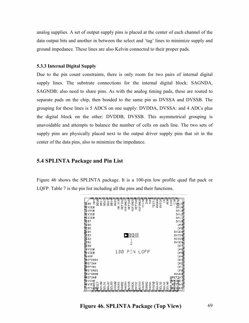
69
analog supplies. A set of output supply pins is placed at the center of each channel of the
data output bits and another in between the select and ‘tag’ lines to minimize supply and
ground impedance. These lines are also Kelvin connected to their proper pads.
5.3.3 Internal Digital Supply
Due to the pin count constraints, there is only room for two pairs of internal digital
supply lines. The substrate connections for the internal digital block: SAGNDA,
SAGNDB: also need to share pins. As with the analog timing pads, these are routed to
separate pads on the chip, then bonded to the same pin as DVSSA and DVSSB. The
grouping for these lines is 5 ADCS on one supply: DVDDA, DVSSA: and 4 ADCs plus
the digital block on the other: DVDDB, DVSSB. This asymmetrical grouping is
unavoidable and attempts to balance the number of cells on each line. The two sets of
supply pins are physically placed next to the output driver supply pins that sit in the
center of the data pins, also to minimize the impedance.
5.4 SPLINTA Package and Pin List
Figure 46 shows the SPLINTA package. It is a 100-pin low profile quad flat pack or
LQFP. Table 7 is the pin list including all the pins and their functions.
Figure 46. SPLINTA Package (Top View)

70
SPLINTA PIN LIST 2/22/2007
Name Function Notes
1 DB8 Channel B CMOS digital output bit 8
2 DVDDB Power for Internal Digital Power connection for internal digital for ADC0,3,6,7 and the DIG_OUT cell
3 DVSSB GND for Internal Digital Gnd and substrate connection for internal digital of ADC0,3,6,7 and DIG_OUT
4 OVSSB Gnd for Output Digital and Internal ROM Gnd connection for internal ROM of ADC1,4,7 and Channel B Digital Outputs
5 OVDDB Power for Output Digital and Internal ROM Power connection for internal ROM of ADC1,4,7 and Channel B Digital Outputs
6:13 DB7:DB0 Channel B output bitsCMOS digital outputs bits 0-7
14 AVSSB Analog Gnd Gnd connection for analog and timing blocks of ADC1,4,7
15 AVDDB Analog Power Power connection for analog and timing blocks of ADC1,4,7
16 WARP Fastest Mode- All 9 tied together This is mode I would use
17 REFGND4 External Reference GND Connection for ADC4
18 REFIN4 External Reference Connection for ADC4
19 REFIN1 External Reference Connection for ADC1
20 REFGND1 External Reference GND Connection for ADC1
21 REFGND0 External Reference GND Connection for ADC0
22 REFIN0 External Reference Connection for ADC0
23 AVSSC Analog Gnd Gnd connection for analog and timing blocks of ADC0,3,6 and master timer cell
24 AVDDC Analog Power Power connection for analog and timing blocks of ADC0,3,6 and master timer cell
25 IMPULSE Slowest Mode Don't need it for operation but used in calibration
26 SARCLK External SAR CLK ~100MHZ for 10 MS/s conversions
27 RESET Reset chip - Aborts current conversion
28:31 SELB0:SELB3 Selects which ADC pair to use for B channel
32:35 TAGB0:TAGB3 Identifier for Channel B
36 BUSYB Indicates when conversions are occuring in B channel
37 OVDDC Power for Output Digital and Internal ROM Power connection for internal ROM of ADC0,3,6,TAG and BUSY Digital Outputs
38 OVSSC Gnd for Output Digital and Internal ROM Gnd connection for internal ROM of ADC0,3,6 ,TAG and BUSY Digital Outputs
39 BUSYA Indicates when conversions are occuring in A channel
40:43 TAGA3:TAGA0 Identifier for Channel A
44:47 SELA3:SELA0 Selects which ADC pair to use for A channel
48 SER_PARB Switches from Serial to parallel mode Always in Parallel mode unless in calibration
49 REFIN3 External Reference Connection for ADC3
50 REFGND3 External Reference GND Connection for ADC3
51 REFGND6 External Reference GND Connection for ADC6
52 REFIN6 External Reference Connection for ADC6
53 REFIN7 External Reference Connection for ADC7
54 REFGND7 External Reference GND Connection for ADC7
55 MODE0 Selects either 16 bit or 18 bit operation Only used in calibration mode
56:63 DA0:DA7 Channel A output bitsCMOS digital outputs bits 0-7
64 OVDDA Power for Output Digital and Internal ROM Power connection for internal ROM of ADC2, 5, 8 and Channel A Digital Outputs
65 OVSSA Gnd for Output Digital and Internal ROM Gnd connection for internal ROM of ADC2, 5, 8 and Channel A Digital Outputs
66 DVSSA GND for Internal Digital Gnd and substrate connection for internal digital of ADC1, 2, 5, 4, 8
67 DVDDA Power for Internal Digital Power connection for internal digital for ADC1, 2, 5, 4, 8
68:75 DA8:DA15 Channel A output bitsCMOS digital outputs bits 8-15
76 BYTE Swaps MSBs and LSBs Used in calibration mode
77 CSB Enables output usually these are tied low All 9 CSB's are tied tog. Needed for cal mode
78 SYNC 10MHz signal Initiate a conversion in sync with SAR CLOCK edge. Conversion start pulse is sent to appropriate ADC pair according to SELA and SELB
79 RDB Control for read. Usually tied low. All 9 RDB's are tied tog. Needed for cal mode
80 PD Powers down ADC Completes current conversion but inhibits subsequent- All 9 tied together
81 AVSSA Analog Gnd Gnd connection for analog and timing blocks of ADC2,5,8
82 AVDDA Analog Power Power connection for analog and timing blocks of ADC2,5,8
83 TEST1 Used selecting certain calibrations
84 INP Positive terminal for ADC input
85 INN Negative terminal for ADC input
86 TEST0 Used selecting certain calibrations
87 REFGND8 External Reference GND Connection for ADC8
88 REFIN8 External Reference Connection for ADC8
89 REFGND5 External Reference GND Connection for ADC5
90 REFIN5 External Reference Connection for ADC5
91 REFGND2 External Reference GND Connection for ADC2
92 REFIN2 External Reference Connection for ADC2
93 OB_2CB Switches from straight binary to 2's comp Used in calibration mode
94:100 DB15:DB9 Channel B output bitsCMOS digital outputs bits 9-15
Table 7 Pin List for SPLINTA

71
6 Conclusion
This thesis described the design of a 4:1 interleaved ADC integrated circuit that
incorporates the ‘split ADC’ concept.. This new architecture has dual digital outputs that
can be used with a background calibration scheme to correct for offset, gain, and timing
errors typically found in interleaved structures. The errors are caused by mismatches
between channels due to physical design and process limitations which will become even
more difficult as process technologies continue to shrink. This split-interleaved ADC
approach together with the calibration algorithm can achieve 16-bit performance at
10MSPS. The correction algorithm uses the difference between the two ADC outputs as
the calibration error signal. An LMS technique is used in a feedback arrangement that
quickly drives the errors to zero. Its deterministic nature allows for fast convergence and
is continuously working in the background. The algorithm can be implemented as an all
digital processor, in an external FPGA or, eventually, in an on-chip digital block.
The purpose of this thesis was to demonstrate the split ADC approach on an interleaved
ADC topology. Design time and risk were minimized by reusing existing designs for
many of the core cells. The AD7621 SAR ADC architecture is used as the core ADC.
The ESD cells and timing block are reused as well. Because most of the cells were
established, proven architectures, the focus of the design could be placed on system level
issues. Practical consideration is given to digital noise and crosstalk, typical in mixed
signal circuits such as SPLINTA. These issues are addressed through a combination of
simulation verification and careful physical layout. Simulations with a shared reference

72
between the ADCs uncovered problems leading to the decision to separate them.
Simulations were not possible for verification of different power supply strategies due to
the difficulty in the DC convergence. The decision was to separate the power supplies
between the analog, internal digital and output driver supplies then further split the
supplies amongst the 16 available pins on the 100-pin package. Limiting the number of
cells sharing the supply lines should reduce crosstalk and ground bounce.
The correction algorithm was demonstrated on the SPLINTA design using a combination
of behavioral level circuit simulations and MATLAB. Mismatch errors were intentionally
introduced in some of the channels and simulated with a sine wave input. The corrupted
data from the dual outputs are imported into the MATLAB calibration program which
completely removes the effect of the mismatches. An FFT of the MATLAB output shows
the noise floor is reduced from -80dB to its ideal value of -120dB in less than 200K
conversions.
SPLINTA is designed to be fabricated on a TSMC 0.25u CMOS process making this chip
suitable to be merged with the digital processor eventually.. The chip is about 7000 um2
and will be packaged in a 100-pin LQFP package. This ADC architecture combined with
the digital correction algorithm offers a solution for a high speed, high resolution self-
calibrating ADC.
6.1 Future Work
SPLINTA is designed to prove the concept of a split-interleaved structure. The next step
is to interface SPLINTA with the hardware for the calibration algorithm currently being
developed in parallel with this work. In lieu of the hardware, the calibration can be
demonstrated the same way as in simulation where data from the dual ADC outputs can
be imported to the MATLAB algorithm for correction. Eventually both SPLINTA and
the calibration hardware must be evaluated together to fully demonstrate the self

73
calibrating ADC system. Ultimately both the digital correction hardware and SPLINTA
could be fabricated on a single chip using standard CMOS technology.
Once the self-calibrating system is successfully demonstrated, the design needs to be
optimized for a more efficient solution. While reuse of the cells is appropriate to verify
the concept, a long term solution should include streamlining the ADC cores. A physical
split in the analog area should be investigated to take advantage of the averaging benefit
of the dual outputs. Also, some of the functions, such as the biasing, may be shared.
Some of the features, such as the lower speed modes, are redundant or not even used. A
comprehensive study of the design and the specific implementation for SPLINTA is
necessary to optimize it for this application.
Another issue with SPLINTA is the excessive number of pins used for the supplies and
references. The goal for SPLINTA is to demonstrate the calibration and it is necessary to
isolate as best as possible to minimize crosstalk and supply noise. However, in order to
make this a viable marketable solution, some effort should be placed on minimizing the
number of pins used for supplies and references. A more sophisticated embedded power
management technique could be investigated to deliver power to the cells such as on-
chip regulators for the supplies and reference. This issue will become increasing
important if both the ADC and digital processor are integrated on the same chip.
Successful evaluation of SPLINTA is the initial step towards a fully integrated, high
speed, high resolution self calibrating ADC.

74
References
[1] W. C. Black Jr. and D. A. Hodges, “Time Interleaved Converter Arrays,” IEEE
Journal of Solid State Circuits, Dec 1980, Volume 15, pp. 1022-1029.
[2] J. McNeill, M. Coln, and B. Larivee, “A Split-ADC Architecture for Deterministic
Digital Background Calibration of a 16b 1MS/s ADC,” IEEE Journal of Solid State
Circuits, Dec 2005, Volume 40, pp. 2437-2445.
[3] R. Allen, “3-Msample/s 16-Bit SAR ADC Sports 1-LSB Accuracy,” ED Online, Feb
2, 2004, ID#7184, http://www.elecdesign.com/Articles/ArticleID/7184/7184.html.
[4] D. Tuite, “SAR ADC Conversion Rates Jump to 4 Msamples/s,” ED Online, July 6,
2006, ID#12935,
http://www.elecdesign.com/Articles/Index.cfm?AD=1&ArticleID=12935.
[5] J. McNeill, C. David, R. Croughwell, M. Coln, and B. Larivee, “Self-Calibration of a
High Resolution Interleaved ADC using the “Split ADC” Architecture,” Analog Devices
Limerick Engineering Conference, November 16, 2006.
[6] Data Sheet, “16-Bit, 2LSB INL, 3 MSPS PulSAR ADC, AD7621,” Analog Devices,
http://www.analog.com/UploadedFiles/Data_Sheets/AD7621.pdf.
[7] W. Kester, “ADC Input Noise: The Good, The Bad, and The Ugly. Is No Noise Good
Noise,” Analog Dialog, Volume 40-02, February 2006.
http://www.analog.com/library/analogdialogue/archives/40-02/adc_noise.html.
[8] H. Jin, E. Lee, and M. Hassoun, “Time-Interleaved A/D Converter with Channel
Randomization,” IEEE Symposium on Circuits and Systems, June 1997, pp. 425-428.
[9] H. Jin and E. Lee, “A Digital-Background Calibration Technique for Minimizing
Timing-Error Effects in Time-Interleaved ADC’s,” IEEE Transactions on Circuits and
75
Systems II: Analog and Digital Signal Processing, Volume 47, No. 7, July 2000,pp. 603-
613.
[10] M. Looney, “Advanced Digital Post-Processing Techniques Enhance Performance in
Time-Interleaved ADC Systems,” Analog Dialog, Volume 37-08, August 2003.
http://www.analog.com/library/analogDialogue/archives/37-08/post_processing.html.
[11] J. Elbornsson and F. Gustafsson, “Analysis of Mismatch Noise in Randomly
Interleaved ADC System,” IEEE International Conference on Acoustics, Speech and
Signal Processing, April 2003, pp. VI-277 -VI-280.
[12] E. Iroaga and B. Murmann, “A Background Correction Technique for Timing Errors
in Time-Interleaved Analog-to-Digital Converters,” IEEE Symposium on Circuits and
Systems, May 2005, Volume 6, pp. 5557-5560.
[13] J. Elbornsson, F. Gustafsson, and J. Eklund, “Blind Equalization of Time Errors in a
Time-Interleaved ADC System,” IEEE Transactions on Signal Processing, April 2005,
Volume 53, No. 4, April 2005.
[14] M. Holdaway, “Understanding an ADC’s FOM,” Electronics Products, April 2006,
http://www.electronicproducts.com/Showpage.asp?Filename=xignal.apr2006.html.
[15] B. Brannon and A. Barlow, “Aperture Uncertainty and ADC System Performance,”
Analog Devices Application Note, AN-501, 2006.
[16] C. Vogel and H. Johansson, “Time-Interleaved Analog-To-Digital Converters:
Status and Future Directions,” IEEE Symposium on Circuits and Systems, May 2006, pp.
3386-3389.

76
[17] M. Tamba, A. Shimizu, H. Munakata and T. Komuro, “A Method to Improve SFDR
with Random Interleaved Sampling Method,” IEEE International Test Conference, Nov.
2001, pp 512-519.
[18] D. Fu, K. Dyer, S. Lewis and P. Hurst, “A Digital-Background Calibration
Technique for Time-Interleaved Analog-to-Digital Converters,” IEEE Journal of Solid-
State Circuits, Volume 33, No. 12, Dec. 1998, pp. 1904-1910.
[19] J. Eklund and F. Gustafsson, “Digital Offset Compensation of Time-Interleaved
ADC Using Random Chopper Sampling,” IEEE Symposium on Circuits and Systems,
May 2000, pp. 447-450.
[20] S. Jamal, D. Fu, N. Chang, P. Hurst and Stephen Lewis, “A 10-b 120-Msample/s
Time-Interleaved Analog-to-Digital Converter With Digital Background Calibration,”
IEEE Journal of Solid-State Circuits, Volume 37, No. 12, Dec. 2002, pp. 1618-1626.
[21] J. Elbornsson, F. Gustafsson, and J. Ekland, “Blind Adaptive Equalization of
Mismatch Errors in a Time-Interleaved A/D Converter System,” IEEE Transactions on
Circuits and Systems I: Regular Papers, Volume 51, No. 1, January 2004, pp. 151-158.
[22] I. Galton, “Digital Cancellation of D/A Converter Noise in Pipelined A/D
Converters,” IEEE Transactions on Circuits and Systems II: Analog and Digital Signal
Processing, Volume 47, Issue 3, March 2000, pp. 185-196.
[23] B. Murmann and B. Boser, “A 12 Bit 75 MS/s Pipelined ADC Using Open-Loop
Residue Amplification,” IEEE International Solid-State Circuits Conference Digest of
Technical Papers, Feb. 2003, pp.328-329.
[24] H. Liu, Z. Lee, and J. Wu, “A 15 b 20 MS/s CMOS Pipelined ADC with Digital
Background Calibration,” IEEE International Solid-State Circuits Conference Digest of
Technical Papers, Feb. 2004, pp. 454-455.

77
[25] K. Nair and R. Harjani, “A 96dB SFDR 50MS/s Digitally Enhanced CMOS
Pipelined A/D Converter,” IEEE International Solid-State Circuits Conference Digest of
Technical Papers, Feb. 2004, pp. 456-457.
[26] S. Ryu, S. Ray, B. Song, G. Cho, and K. Bacrania, “A 14 b-linear capacitor self-
trimming pipelined ADC”, IEEE International Solid-State Circuits Conference Digest of
Technical Papers, Feb. 2004, pp. 464-465.
[27] D. Johns and K. Martin, Analog Integrated Circuit Design. New York: John Wiley
& Sons, 1997
[28] W. Kester, “Tutorial MT-021: ADC Architectures II: Successive Approximation
ADCs,” http://www.analog.com/en/content/0,2886,760%255F788%255F92112,00.html.
[29] AD7621 Design Team, “AD7621 Design Review: Timing Generator and I/O Pad
Cells”, Unpublished Design Review Presentation, Analog Devices Internal, Jan 2003.
[30] Application Note, “AN-640 Understanding and Minimizing Ground Bounce,”
Fairchild Semiconductor, Feb 2003.
[31] G. Carreau, “AD7625: A 10MHz 16-bit Time Interleaved ADC: Test Chip
Architecture/Design Review”, Unpublished Design Review Presentation, Analog Devices
Internal, Aug 2005.
[32] W. Sansen, Analog Design Essentials, Dordrecht, The Netherlands: Springer, 2006
[33] N. Karim, A. Agrawal, “Plastic Packages’ Electrical Performance: Reduced Bond
Wire Diameter” Amkor White Paper,
http://www.amkor.com/services/electrical/newabstr.pdf
78
Appendix A
Linearity Calibration
Each ADC in the interleaved system includes the capability to be calibrated for linearity.
Non-idealities in the linearity are caused by bit errors which are the result of mismatches
in the capacitor DAC arrays. One of the advantages of this type of architecture is that
adjustments can be made relatively easily and inexpensively by digitally switching in
small values of capacitances to compensate for those mismatches. The SPLINTA ADCs
can be configured to program these correction values through the DOUTA data lines.
The algorithm is based on the assumption that the ADC digital output is always all zeros
at negative full scale and always all ones at positive full scale and therefore the overall
gain of the ADC is inherently perfect. This assumption is true because of the way in
which the charge redistribution capacitor DAC is designed (sec 3.1.4.1). If any bit errors
exist it will cause problems for the integral linearity (INL), not the gain, and they must be
corrected in such a way that the overall gain is maintained. The gain can be preserved if,
for each individual bit error, the correction is distributed so that there is no net change. In
other words, for each bit error measured, -1/2*ERROR is assigned to the bit under test
and +1/2*ERROR is binarily distributed to the lower bits [A1, A2].
For example, if an INL test showed a +48 LSB error at the code 32768 (215=MSB), then
the bit error at the MSB=48LSBs. To correct for this, the error is distributed as follows:
MSB Correction = -24LSB; BIT 2 = +12LSB; BIT 3 = +6; BIT 4 = +3; etc.
Clearly, errors in the lower bits will affect the higher bit measurements and need to be
accounted for when determining the correction factors. Also, since the corrections need to
be distributed as described above, superposition is be used to determine the final
corrections.

79
The basic flow for the calibration procedure is summarized below, followed by a ‘user’s
guide’ detailing a step by step procedure to measure, calculate and program the
corrections.
Calibration Summary
1. Select ADC to calibrate
2. Measure bit errors
3. Determine actual bit error corrections
4. Determine codes for each location
5. Program each location
6. Retest INL
1. Select ADC to Calibrate
Each converter is calibrated individually and is done through the A channel.
The ADC to be calibrated can be selected by setting the SELA bus appropriately. Initially
the ADC should be in the normal mode, both TEST pins set low.
2. Measure Bit Errors
The bit errors can be determined by measuring the INL of the ADC and recording any
errors seen at the appropriate codes. The ADC has two redundancy bits between bits 7
and 8, (7x), and 12 and 13, (12x). Because of these extra bits, the actual bit locations for
the top 7 bits are offset by 256+8. For example, the location for the MSB is
215+256+8=33032. For bits 7x -12, the codes are offset by 8 and bits 12x to 16 are not
offset at all. The correction for the bottom eight bits are distributed over three locations
based on the two measurements at locations 520 and 32. The adjusted codes values for
the bit locations are listed in Table A1.

80
N BIT Error Locations CODE Measured Bit Error
1 1(MSB) 33032 BEmeas1
2 2 16648 BEmeas2
3 3 8456 BEmeas3
4 4 4360 BEmeas4
5 5 2304 BEmeas5
6 6 1288 BEmeas6
7 7 776 BEmeas7
8 8-12 520 BEmeas8
9 13-16(LSB) 32 BEmeas9
3. Determine Actual Bit Errors
The errors from the lower bits will affect the higher bits and can be either corrected for
individually or subtracted out of the higher bits to determine the actual errors. The
individual errors can be determined by successively subtracting out the lower bit errors
from the higher bit errors. For example, starting with the lowest bits, the error at location
32 is subtracted out from the error at location 520 to get the actual error of bits 8-12.
Then the sum of the errors at 520 and 32 is subtracted from the measured value at 776 to
get the actual value at bit 7. The sum of errors at 776, 520 and 32, is subtracted from the
error at 1288, and so on. The corrections for each bit can be calculated by equation A1.
99
8
)1( 1:8
measact
n
nactmeasnactn
BEBE
nBEBEBE
=
=−= ∑ +
(A1)
4. Determine Codes for Each Location
Once all the adjusted errors are known, the correction codes for each of the nine locations
are calculated using Eq A2.
128×= actnn BECorrection (A2)
TABLE A1. Bit Codes for Calibration

81
Superposition is necessary to calculate the final correction factors because half of each bit
correction is spread over the lower bits. The calculations for the top 7 capacitor locations
are as follows:
( )
( )2/77
2/6212/7
2/212/3
2/12/2
2/1
7
3
2
1
CAPxCAP
CAPCAPCAPCorrectionCAP
CAPCAPCorrectionCAP
CAPCorrectionCAP
CorrectionCAP
−=
++−−=
•
•
•
+−−=
−−=
−=
L
(A3)
The residual error in CAP7x is distributed to the lower bits and since there are only three
correction locations for the lower bits, they are calculated as follows:
8/12/2
2/82/1
2/72/8
9
9
8
CcBECc
CAPCorrectionCc
xCAPCorrectionCAP
meas −−=
−−=
−−=
(A4)
The correction code is a 12 bit signed code. The 12th bit is used for the sign; negative
numbers need 4096 added to them to obtain the programmed correction code. For
example, -320 is programmed as 4096 – 320 = 3776.
5. Program Each Location
Each ADC has its own programmable memory. The mapping is shown in table A2.

82
ROM ADDRESS LOCATION NAME3 CAP1 (MSB)
4 CAP2
5 CAP3
6 CAP4
7 CAP5
8 CAP6
9 CAP7
10 CAP7x
11 CAP8
12 Cc1
13 Cc2
Some of the pins are reassigned in this mode and used as the address pins: A[3] =
PWRDDN, A[2]=BYTE, A[1]=WARP, A[0]=IMPULSE. Digital outputs are bi-
directional and used to program data to ROM. The calibration mode signals are
sequenced as shown below to program the corrections into memory:
a. TEST[1:0]=11
b. CSB=0
c. RDB=1
d. A[3:0]=ROM address to correct bit Table A2.
e. DA[11:0] = Correction code
f. CNVST 1>0 to Load
g. RDB = 0 to read code back (optional)
a. The test pins need to both be set high to disable the normal mode enabling the
ROM mode. The selection lines for Channel A will determine which ADC will be
programmed.
b. The chip select line CSB is set low only on the ADC under test so that only it’s
memory gets programmed.
c. The read pin is set high to enable the ‘write’ mode through the data output pins.
TABLE A2. ROM Address for CAP Adjustments

83
d. The correct location is selected through the reassigned address pins: A[3] =
PWRDDN, A[2]=BYTE, A[1]=WARP, A[0]=IMPULSE.
e. The correction code is a 12 bit signed code.
f. The CSB line is brought low to apply the code.
g. If desired, the RDB line can be brought back low to read back the programmed
code from the A channel data output pins.
6. Retest INL
Once all the coefficients are applied, the INL should be rechecked. Some adjustments,
particularly to the lower bits, may be necessary.
[A1] H-S Lee, D. A. Hodges, P. R. Gray, “A Self-Calibrating 15 Bit CMOS A/D
Converter,” IEEE Journal of Solid-State Circuits, Volume SC-19, No. 6, Dec. 1984, pp.
813-819.
[A2] AD7621 Design Team, “AD7621 Digital Design Review”, Unpublished Design
Review Presentation, Analog Devices Internal, Jan 2003.
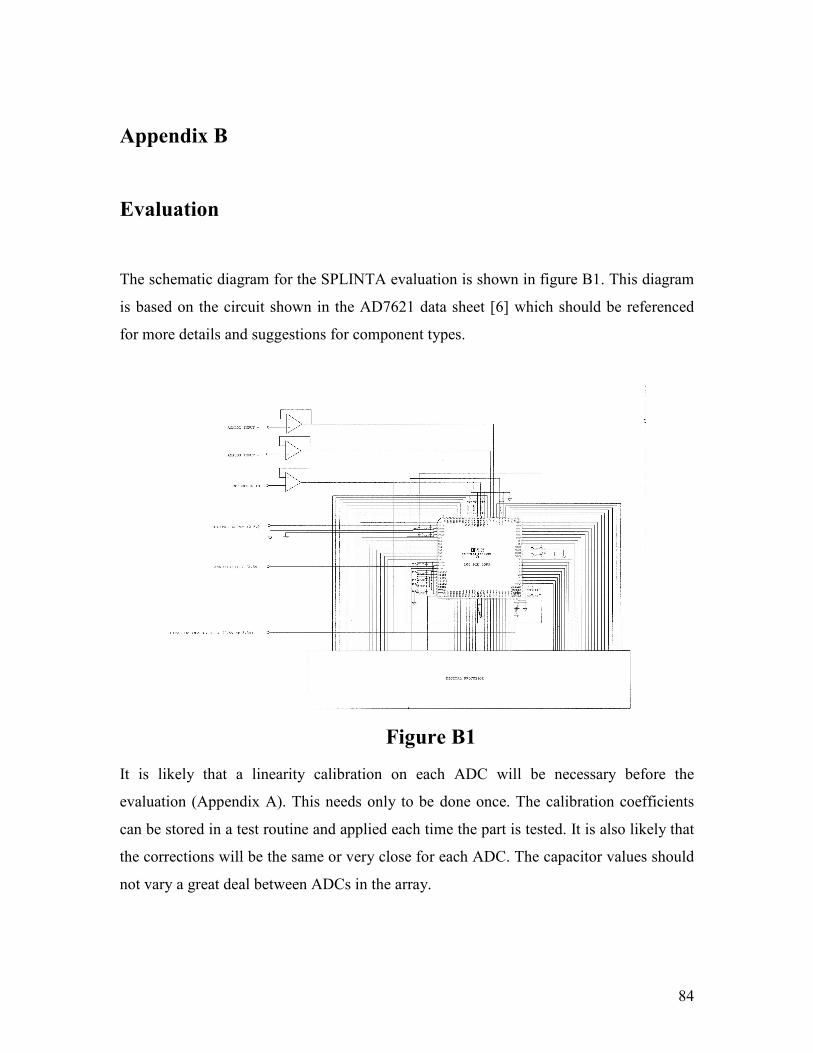
84
Appendix B
Evaluation
The schematic diagram for the SPLINTA evaluation is shown in figure B1. This diagram
is based on the circuit shown in the AD7621 data sheet [6] which should be referenced
for more details and suggestions for component types.
It is likely that a linearity calibration on each ADC will be necessary before the
evaluation (Appendix A). This needs only to be done once. The calibration coefficients
can be stored in a test routine and applied each time the part is tested. It is also likely that
the corrections will be the same or very close for each ADC. The capacitor values should
not vary a great deal between ADCs in the array.
Figure B1

85
The performance of SPLINTA as a stand alone ADC depends on the quality of the
physical layout and the matching between the channels. The hardware for the calibration
algorithm (sec.2.3.2) should be used to fully evaluate the performance of system which is
expected to be equivalent to the performance reported in the AD7621 data sheet.
In the absence of this hardware, data from the dual outputs of SPLINTA can be imported
into the MATLAB program containing the correction algorithm. The output from the
MATLAB program can be used to evaluate the performance.
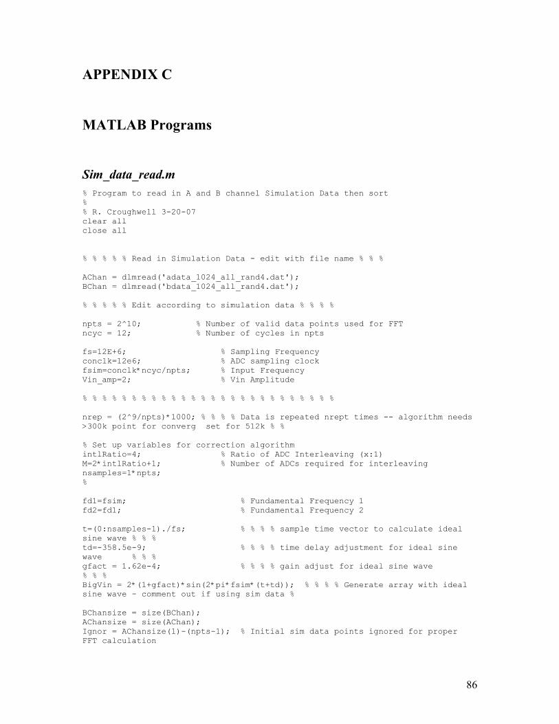
86
APPENDIX C
MATLAB Programs
Sim_data_read.m
% Program to read in A and B channel Simulation Data then sort % % R. Croughwell 3-20-07 clear all close all % % % % % Read in Simulation Data - edit with file name % % % AChan = dlmread('adata_1024_all_rand4.dat'); BChan = dlmread('bdata_1024_all_rand4.dat'); % % % % % Edit according to simulation data % % % % npts = 2^10; % Number of valid data points used for FFT ncyc = 12; % Number of cycles in npts fs=12E+6; % Sampling Frequency conclk=12e6; % ADC sampling clock fsim=conclk*ncyc/npts; % Input Frequency Vin_amp=2; % Vin Amplitude % % % % % % % % % % % % % % % % % % % % % % % % % % nrep = (2^9/npts)*1000; % % % % Data is repeated nrept times -- algorithm needs >300k point for converg set for 512k % % % Set up variables for correction algorithm intlRatio=4; % Ratio of ADC Interleaving (x:1) M=2*intlRatio+1; % Number of ADCs required for interleaving nsamples=1*npts; % fd1=fsim; % Fundamental Frequency 1 fd2=fd1; % Fundamental Frequency 2 t=(0:nsamples-1)./fs; % % % % sample time vector to calculate ideal sine wave % % % td=-358.5e-9; % % % % time delay adjustment for ideal sine wave % % % gfact = 1.62e-4; % % % % gain adjust for ideal sine wave % % % BigVin = 2*(1+gfact)*sin(2*pi*fsim*(t+td)); % % % % Generate array with ideal sine wave - comment out if using sim data % BChansize = size(BChan); AChansize = size(AChan); Ignor = AChansize(1)-(npts-1); % Initial sim data points ignored for proper FFT calculation

87
% BigVin = AChan(Ignor:AChansize,2); % % Load first npts of Input samples collected by the datalog in simulation % % % Comment out if using ideal data % % Load first npts of B channel ouput and tag % % BigBDout=BChan(Ignor:BChansize,4); BigBpick=BChan(Ignor:BChansize,1)+1; BigBVout = (2*BigBDout*2.048/2^16)-2.048; % % Calculate analog output % % % % Load first npts of A channel ouput and tag % % BigADout=AChan(Ignor:AChansize,4); BigApick=AChan(Ignor:AChansize,1)+1; BigAVout = (2*BigADout*2.048/2^16)-2.048; % % Calculate analog output % % lngVout=nrep*nsamples; % % % % number of data points for xi = 1:nrep repindex = xi * nsamples; BigVin(repindex+1:repindex+nsamples) = BigVin(1:nsamples); BigBDout(repindex+1:repindex+nsamples) = BigBDout(1:nsamples); BigBpick(repindex+1:repindex+nsamples) =BigBpick(1:nsamples); BigBVout(repindex+1:repindex+nsamples) =BigBVout(1:nsamples); BigADout(repindex+1:repindex+nsamples) = BigADout(1:nsamples); BigApick(repindex+1:repindex+nsamples) =BigApick(1:nsamples); BigAVout(repindex+1:repindex+nsamples) =BigAVout(1:nsamples); end Vin = BigVin; BDout=BigBDout; Bpick=BigBpick; Bpick=Bpick'; BVout = BigBVout; ADout=BigADout; Apick=BigApick; Apick=Apick'; AVout = BigAVout; nsamples=lngVout; Vout(:,1) = AVout; Vout(:,2) = BVout; Vout = Vout'; Voutadc = (BigBVout+BigBVout)/2;

88
Multi_ADC_cor06.m
%************************************************************************** % Iterative Correction Algorithm for the Multi Interleaved ADC Vers. 06 % 2006.11.06 % % This program builds up the deltaX values for finding the gain, offset % and aperture delay, errors in the Multi Interleaved, Split ADC % architecture. A coefficient matrix is also built for testing and % debugging purposes. % % This program also computes the RMS Error between the Ideal and Corrected % output. % % For use with the multi_ADC_setup06. % %************************************************************************** % Estimation Loop Parameters % mx is the step size in the Gain and Offset error estimation mxrecip=128; mx=1/mxrecip; %Step size of approaching the Estimated Error myrecip=64; my=1/myrecip; Ncoef=128; % Number of conversions used to build up matrices jacobLeng=floor(nsamples/Ncoef); %Number of main loops %************************************************************************** %************************************************************************** %************************************************************************** % Note to Rosa: % Vout Setup % This code is for combining two separate Raw (uncorrected) Vout vectors % into one (1) Raw Vout vector. Namely, this is for taking a VoutA and a % VoutB and combining them into a single variable that this program uses. % The setup program, multi_ADC_setup06, outputs one Vout variable with two % rows, A and B. % Uncomment this code to use it % Vout = [VoutA; VoutB]; % Initialize all Matrices to make room in Memory and save time VoutA=zeros(1,(jacobLeng-1)*Ncoef+1); VoutB=zeros(1,(jacobLeng-1)*Ncoef+1); VoutBad=zeros(1,(jacobLeng-1)*Ncoef+1); VoutCorA=zeros(1,(jacobLeng-1)*Ncoef+1); VoutCorB=zeros(1,(jacobLeng-1)*Ncoef+1); VoutCor=zeros(1,(jacobLeng-1)*Ncoef+1); %EATPD=[t_apd1;t_apd2;t_apd3;t_apd4;t_apd5].*10E6; % Real Aperture coefficients Eg_est=zeros(M,1); % Initialize all Error Estimates to zero Eg_eps=zeros(M,1);
89
Eos_est=zeros(M,1); Eos_eps=zeros(M,1); Etpd_est=zeros(M,1); % Initialize all Error Estimates to zero Etpd_eps=zeros(M,1); % Initialize Error in the Estimate to zero jacobLeng=floor(nsamples/Ncoef); RMS_Convergence=zeros(1,jacobLeng-1); tempRMS_0=zeros(1,Ncoef-2); tempRMS=zeros(1,Ncoef); j=1; % Initialize the coefficients and bins matrices to zero Eos_coef=zeros(Ncoef,M); % Initialize Offset Error Coefficients matrix Eg_coef=zeros(Ncoef,M); % Initialize Gain Error Coefficients matrix Etpd_coef=zeros(Ncoef,M); Eos_bins=zeros(1,M); Eg_bins=zeros(1,M); Etpd_bins=zeros(1,M); deltaX=zeros(Ncoef+3,1); %Initialize the Plus or Minus Matrix with the data from the A & B Tags pmmat=zeros(M,lngVout); for (i=1:lngVout) pmmat(Apick(i),i)=-1; pmmat(Bpick(i),i)=1; end % Fill up the first two samples of the uncorrected vectors using Vout VoutA(1:3)=[Vout(1,1) Vout(1,2), Vout(1,3)]; VoutB(1:3)=[Vout(2,1) Vout(2,2), Vout(2,3)]; VoutBad(1:3)=(VoutA(1:3)+VoutB(1:3))/2; deltaX(1:2)=VoutB(1:2)-VoutA(1:2); for (i=3:Ncoef) k=(Ncoef*(j-1)+i); % Generate the proper index for the Apick and % Bpick matrices to keep track of ADC A and % ADC B VoutA(k+1)=Vout(1,k+1)-Eos_est(Apick(k+1)); % Correct for G and OS VoutA(k+1)=VoutA(k+1)/(1+Eg_est(Apick(k+1))); VoutB(k+1)=Vout(2,k+1)-Eos_est(Bpick(k+1)); VoutB(k+1)=VoutB(k+1)/(1+Eg_est(Bpick(k+1))); VoutA(k+2)=Vout(1,k+2)-Eos_est(Apick(k+2)); % Correct for G and OS VoutA(k+2)=VoutA(k+2)/(1+Eg_est(Apick(k+2))); VoutB(k+2)=Vout(2,k+2)-Eos_est(Bpick(k+2)); VoutB(k+2)=VoutB(k+2)/(1+Eg_est(Bpick(k+2))); %VoutA(k+1)=Vout(Apick(k+1),k+1); %VoutB(k+1)=Vout(Bpick(k+1),k+1); VoutBad(k+1:k+2)=(VoutA(k+1:k+2)+VoutB(k+1:k+2))/2; %deltaConv=(VoutBad(k+1)-VoutBad(k-1))/2; % Get Average Delta Conversion % deltaConv is not the same as deltaX deltaConv is the derivative % estimate. deltaX is the difference between the A and B outputs deltaConv=(VoutBad(k+1)-VoutBad(k-1))*(2/3)+... (VoutBad(k-2)-VoutBad(k+2))*(1/12); % Get Average Delta Conversion VoutCorA(k)=VoutA(k)-Etpd_est(Apick(k))*deltaConv; VoutCorB(k)=VoutB(k)-Etpd_est(Bpick(k))*deltaConv; VoutCor(k)=(VoutCorA(k)+VoutCorB(k))/2; % Get Average Corrected Output deltaX(i)=(VoutCorB(k)-VoutCorA(k)); % Get difference between % corrected outputs Eos_coef(i,:)=pmmat(:,k)'; Eg_coef(i,:)=VoutCor(k)*pmmat(:,k)'; Etpd_coef(i,:)=deltaConv*pmmat(:,k)'; % Collect Coefficients Eos_bins=(sign(Eos_coef(i,:))*deltaX(i))+Eos_bins;

90
Eg_bins=(sign(Eg_coef(i,:))*deltaX(i))+Eg_bins; Etpd_bins=(sign(Etpd_coef(i,:))*deltaX(i))+Etpd_bins; tempRMS_0(i)=VoutCorB(k)-VoutCorA(k); end E_coef=[Eos_coef Eg_coef Etpd_coef]; E_coef=[E_coef; [ones(1,M),zeros(1,2*M)]; [zeros(1,M),ones(1,M),zeros(1,M)];... [zeros(1,2*M),ones(1,M)]]; % Calculate and track the Error in the Estimate Eos_eps=(1-mx)*Eos_eps+Eos_bins'*mx; Eg_eps=(1-mx)*Eg_eps+Eg_bins'*mx; Etpd_eps=(1-mx)*Etpd_eps+Etpd_bins'*mx; Eos_eps_track(:,j)=Eos_eps; Eg_eps_track(:,j)=Eg_eps; Etpd_eps_track(:,j)=Etpd_eps; % Calculate and track the Estimate Eos_est=my.*Eos_eps+Eos_est; Eg_est=my.*Eg_eps+Eg_est; Etpd_est=my.*Etpd_eps+Etpd_est; Eos_est_track(:,j)=Eos_est; Eg_est_track(:,j)=Eg_est; Etpd_est_track(:,j)=Etpd_est; RMS_Convergence(1)=sum(tempRMS_0.^2)/length(tempRMS_0); jacobLeng=floor(nsamples/Ncoef); for (j=2:jacobLeng-1) % Initialize the coefficients and bins matrices to zero Eos_coef=zeros(Ncoef,M); % Initialize Offset Error Coefficients matrix Eg_coef=zeros(Ncoef,M); % Initialize Gain Error Coefficients matrix Etpd_coef=zeros(Ncoef,M); Eos_bins=zeros(1,M); Eg_bins=zeros(1,M); Etpd_bins=zeros(1,M); deltaX=zeros(Ncoef+3,1); for (i=1:Ncoef) k=(Ncoef*(j-1)+i); % Generate the proper index for the Apick and % Bpick matrices to keep track of ADC A and % ADC B VoutA(k+1)=Vout(1,k+1)-Eos_est(Apick(k+1)); % Correct for G and OS VoutA(k+1)=VoutA(k+1)/(1+Eg_est(Apick(k+1))); VoutB(k+1)=Vout(2,k+1)-Eos_est(Bpick(k+1)); VoutB(k+1)=VoutB(k+1)/(1+Eg_est(Bpick(k+1))); VoutA(k+2)=Vout(1,k+2)-Eos_est(Apick(k+2)); % Correct for G and OS VoutA(k+2)=VoutA(k+2)/(1+Eg_est(Apick(k+2))); VoutB(k+2)=Vout(2,k+2)-Eos_est(Bpick(k+2)); VoutB(k+2)=VoutB(k+2)/(1+Eg_est(Bpick(k+2))); %VoutA(k+1)=Vout(Apick(k+1),k+1); %VoutB(k+1)=Vout(Bpick(k+1),k+1); VoutBad(k+1:k+2)=(VoutA(k+1:k+2)+VoutB(k+1:k+2))/2; %deltaConv=(VoutBad(k+1)-VoutBad(k-1))/2; % Get Average Delta Conversion deltaConv=(VoutBad(k+1)-VoutBad(k-1))*(2/3)+... (VoutBad(k-2)-VoutBad(k+2))*(1/12); % Get Average Delta Conversion VoutCorA(k)=VoutA(k)-Etpd_est(Apick(k))*deltaConv; VoutCorB(k)=VoutB(k)-Etpd_est(Bpick(k))*deltaConv;
91
VoutCor(k)=(VoutCorA(k)+VoutCorB(k))/2; % Get Average Corrected Output deltaX(i)=(VoutCorB(k)-VoutCorA(k)); % Get difference between % corrected outputs Eos_coef(i,:)=pmmat(:,k)'; Eg_coef(i,:)=VoutCor(k)*pmmat(:,k)'; Etpd_coef(i,:)=deltaConv*pmmat(:,k)'; % Collect Coefficients Eos_bins=(sign(Eos_coef(i,:))*deltaX(i))+Eos_bins; Eg_bins=(sign(Eg_coef(i,:))*deltaX(i))+Eg_bins; Etpd_bins=(sign(Etpd_coef(i,:))*deltaX(i))+Etpd_bins; tempRMS(i)=VoutCorB(k)-VoutCorA(k); %Get difference for RMS Convergence end E_coef=[Eos_coef Eg_coef Etpd_coef]; E_coef=[E_coef; [ones(1,M),zeros(1,2*M)]; [zeros(1,M),ones(1,M),zeros(1,M)];... [zeros(1,2*M),ones(1,M)]]; % Coefficient matrix with averaging % Calculate and track the Error in the Estimate Eos_eps=(1-mx)*Eos_eps+Eos_bins'*mx; Eg_eps=(1-mx)*Eg_eps+Eg_bins'*mx; Etpd_eps=(1-mx)*Etpd_eps+Etpd_bins'*mx; Eos_eps_track(:,j)=Eos_eps; Eg_eps_track(:,j)=Eg_eps; Etpd_eps_track(:,j)=Etpd_eps; % Calculate and track the Estimate Eos_est=my.*Eos_eps+Eos_est; Eg_est=my.*Eg_eps+Eg_est; Etpd_est=my.*Etpd_eps+Etpd_est; Eos_est_track(:,j)=Eos_est; Eg_est_track(:,j)=Eg_est; Etpd_est_track(:,j)=Etpd_est; % Compute RMS Error RMS_Convergence(j)=sum(tempRMS.^2)/Ncoef; end

92
Sim_data_plot.m
%************************************************************************** % Iterative Correction Algorithm for the Multi Interleaved ADC Vers. 06 % 2006.11.06 % % This program builds up the deltaX values for finding the gain, offset % and aperture delay, errors in the Multi Interleaved, Split ADC % architecture. A coefficient matrix is also built for testing and % debugging purposes. % % This program also computes the RMS Error between the Ideal and Corrected % output. % % For use with the multi_ADC_setup06. % %************************************************************************** % Estimation Loop Parameters % mx is the step size in the Gain and Offset error estimation mxrecip=128; mx=1/mxrecip; %Step size of approaching the Estimated Error myrecip=64; my=1/myrecip; Ncoef=128; % Number of conversions used to build up matrices jacobLeng=floor(nsamples/Ncoef); %Number of main loops %************************************************************************** %************************************************************************** %************************************************************************** % Note to Rosa: % Vout Setup % This code is for combining two separate Raw (uncorrected) Vout vectors % into one (1) Raw Vout vector. Namely, this is for taking a VoutA and a % VoutB and combining them into a single variable that this program uses. % The setup program, multi_ADC_setup06, outputs one Vout variable with two % rows, A and B. % Uncomment this code to use it % Vout = [VoutA; VoutB]; % Initialize all Matrices to make room in Memory and save time VoutA=zeros(1,(jacobLeng-1)*Ncoef+1); VoutB=zeros(1,(jacobLeng-1)*Ncoef+1); VoutBad=zeros(1,(jacobLeng-1)*Ncoef+1); VoutCorA=zeros(1,(jacobLeng-1)*Ncoef+1); VoutCorB=zeros(1,(jacobLeng-1)*Ncoef+1); VoutCor=zeros(1,(jacobLeng-1)*Ncoef+1); %EATPD=[t_apd1;t_apd2;t_apd3;t_apd4;t_apd5].*10E6; % Real Aperture coefficients Eg_est=zeros(M,1); % Initialize all Error Estimates to zero Eg_eps=zeros(M,1); Eos_est=zeros(M,1); Eos_eps=zeros(M,1); Etpd_est=zeros(M,1); % Initialize all Error Estimates to zero

93
Etpd_eps=zeros(M,1); % Initialize Error in the Estimate to zero jacobLeng=floor(nsamples/Ncoef); RMS_Convergence=zeros(1,jacobLeng-1); tempRMS_0=zeros(1,Ncoef-2); tempRMS=zeros(1,Ncoef); j=1; % Initialize the coefficients and bins matrices to zero Eos_coef=zeros(Ncoef,M); % Initialize Offset Error Coefficients matrix Eg_coef=zeros(Ncoef,M); % Initialize Gain Error Coefficients matrix Etpd_coef=zeros(Ncoef,M); Eos_bins=zeros(1,M); Eg_bins=zeros(1,M); Etpd_bins=zeros(1,M); deltaX=zeros(Ncoef+3,1); %Initialize the Plus or Minus Matrix with the data from the A & B Tags pmmat=zeros(M,lngVout); for (i=1:lngVout) pmmat(Apick(i),i)=-1; pmmat(Bpick(i),i)=1; end % Fill up the first two samples of the uncorrected vectors using Vout VoutA(1:3)=[Vout(1,1) Vout(1,2), Vout(1,3)]; VoutB(1:3)=[Vout(2,1) Vout(2,2), Vout(2,3)]; VoutBad(1:3)=(VoutA(1:3)+VoutB(1:3))/2; deltaX(1:2)=VoutB(1:2)-VoutA(1:2); for (i=3:Ncoef) k=(Ncoef*(j-1)+i); % Generate the proper index for the Apick and % Bpick matrices to keep track of ADC A and % ADC B VoutA(k+1)=Vout(1,k+1)-Eos_est(Apick(k+1)); % Correct for G and OS VoutA(k+1)=VoutA(k+1)/(1+Eg_est(Apick(k+1))); VoutB(k+1)=Vout(2,k+1)-Eos_est(Bpick(k+1)); VoutB(k+1)=VoutB(k+1)/(1+Eg_est(Bpick(k+1))); VoutA(k+2)=Vout(1,k+2)-Eos_est(Apick(k+2)); % Correct for G and OS VoutA(k+2)=VoutA(k+2)/(1+Eg_est(Apick(k+2))); VoutB(k+2)=Vout(2,k+2)-Eos_est(Bpick(k+2)); VoutB(k+2)=VoutB(k+2)/(1+Eg_est(Bpick(k+2))); %VoutA(k+1)=Vout(Apick(k+1),k+1); %VoutB(k+1)=Vout(Bpick(k+1),k+1); VoutBad(k+1:k+2)=(VoutA(k+1:k+2)+VoutB(k+1:k+2))/2; %deltaConv=(VoutBad(k+1)-VoutBad(k-1))/2; % Get Average Delta Conversion % deltaConv is not the same as deltaX deltaConv is the derivative % estimate. deltaX is the difference between the A and B outputs deltaConv=(VoutBad(k+1)-VoutBad(k-1))*(2/3)+... (VoutBad(k-2)-VoutBad(k+2))*(1/12); % Get Average Delta Conversion VoutCorA(k)=VoutA(k)-Etpd_est(Apick(k))*deltaConv; VoutCorB(k)=VoutB(k)-Etpd_est(Bpick(k))*deltaConv; VoutCor(k)=(VoutCorA(k)+VoutCorB(k))/2; % Get Average Corrected Output deltaX(i)=(VoutCorB(k)-VoutCorA(k)); % Get difference between % corrected outputs Eos_coef(i,:)=pmmat(:,k)'; Eg_coef(i,:)=VoutCor(k)*pmmat(:,k)'; Etpd_coef(i,:)=deltaConv*pmmat(:,k)'; % Collect Coefficients Eos_bins=(sign(Eos_coef(i,:))*deltaX(i))+Eos_bins; Eg_bins=(sign(Eg_coef(i,:))*deltaX(i))+Eg_bins; Etpd_bins=(sign(Etpd_coef(i,:))*deltaX(i))+Etpd_bins; tempRMS_0(i)=VoutCorB(k)-VoutCorA(k);
94
end E_coef=[Eos_coef Eg_coef Etpd_coef]; E_coef=[E_coef; [ones(1,M),zeros(1,2*M)]; [zeros(1,M),ones(1,M),zeros(1,M)];... [zeros(1,2*M),ones(1,M)]]; % Calculate and track the Error in the Estimate Eos_eps=(1-mx)*Eos_eps+Eos_bins'*mx; Eg_eps=(1-mx)*Eg_eps+Eg_bins'*mx; Etpd_eps=(1-mx)*Etpd_eps+Etpd_bins'*mx; Eos_eps_track(:,j)=Eos_eps; Eg_eps_track(:,j)=Eg_eps; Etpd_eps_track(:,j)=Etpd_eps; % Calculate and track the Estimate Eos_est=my.*Eos_eps+Eos_est; Eg_est=my.*Eg_eps+Eg_est; Etpd_est=my.*Etpd_eps+Etpd_est; Eos_est_track(:,j)=Eos_est; Eg_est_track(:,j)=Eg_est; Etpd_est_track(:,j)=Etpd_est; RMS_Convergence(1)=sum(tempRMS_0.^2)/length(tempRMS_0); jacobLeng=floor(nsamples/Ncoef); for (j=2:jacobLeng-1) % Initialize the coefficients and bins matrices to zero Eos_coef=zeros(Ncoef,M); % Initialize Offset Error Coefficients matrix Eg_coef=zeros(Ncoef,M); % Initialize Gain Error Coefficients matrix Etpd_coef=zeros(Ncoef,M); Eos_bins=zeros(1,M); Eg_bins=zeros(1,M); Etpd_bins=zeros(1,M); deltaX=zeros(Ncoef+3,1); for (i=1:Ncoef) k=(Ncoef*(j-1)+i); % Generate the proper index for the Apick and % Bpick matrices to keep track of ADC A and % ADC B VoutA(k+1)=Vout(1,k+1)-Eos_est(Apick(k+1)); % Correct for G and OS VoutA(k+1)=VoutA(k+1)/(1+Eg_est(Apick(k+1))); VoutB(k+1)=Vout(2,k+1)-Eos_est(Bpick(k+1)); VoutB(k+1)=VoutB(k+1)/(1+Eg_est(Bpick(k+1))); VoutA(k+2)=Vout(1,k+2)-Eos_est(Apick(k+2)); % Correct for G and OS VoutA(k+2)=VoutA(k+2)/(1+Eg_est(Apick(k+2))); VoutB(k+2)=Vout(2,k+2)-Eos_est(Bpick(k+2)); VoutB(k+2)=VoutB(k+2)/(1+Eg_est(Bpick(k+2))); %VoutA(k+1)=Vout(Apick(k+1),k+1); %VoutB(k+1)=Vout(Bpick(k+1),k+1); VoutBad(k+1:k+2)=(VoutA(k+1:k+2)+VoutB(k+1:k+2))/2; %deltaConv=(VoutBad(k+1)-VoutBad(k-1))/2; % Get Average Delta Conversion deltaConv=(VoutBad(k+1)-VoutBad(k-1))*(2/3)+... (VoutBad(k-2)-VoutBad(k+2))*(1/12); % Get Average Delta Conversion VoutCorA(k)=VoutA(k)-Etpd_est(Apick(k))*deltaConv; VoutCorB(k)=VoutB(k)-Etpd_est(Bpick(k))*deltaConv; VoutCor(k)=(VoutCorA(k)+VoutCorB(k))/2; % Get Average Corrected Output deltaX(i)=(VoutCorB(k)-VoutCorA(k)); % Get difference between

95
% corrected outputs Eos_coef(i,:)=pmmat(:,k)'; Eg_coef(i,:)=VoutCor(k)*pmmat(:,k)'; Etpd_coef(i,:)=deltaConv*pmmat(:,k)'; % Collect Coefficients Eos_bins=(sign(Eos_coef(i,:))*deltaX(i))+Eos_bins; Eg_bins=(sign(Eg_coef(i,:))*deltaX(i))+Eg_bins; Etpd_bins=(sign(Etpd_coef(i,:))*deltaX(i))+Etpd_bins; tempRMS(i)=VoutCorB(k)-VoutCorA(k); %Get difference for RMS Convergence end E_coef=[Eos_coef Eg_coef Etpd_coef]; E_coef=[E_coef; [ones(1,M),zeros(1,2*M)]; [zeros(1,M),ones(1,M),zeros(1,M)];... [zeros(1,2*M),ones(1,M)]]; % Coefficient matrix with averaging % Calculate and track the Error in the Estimate Eos_eps=(1-mx)*Eos_eps+Eos_bins'*mx; Eg_eps=(1-mx)*Eg_eps+Eg_bins'*mx; Etpd_eps=(1-mx)*Etpd_eps+Etpd_bins'*mx; Eos_eps_track(:,j)=Eos_eps; Eg_eps_track(:,j)=Eg_eps; Etpd_eps_track(:,j)=Etpd_eps; % Calculate and track the Estimate Eos_est=my.*Eos_eps+Eos_est; Eg_est=my.*Eg_eps+Eg_est; Etpd_est=my.*Etpd_eps+Etpd_est; Eos_est_track(:,j)=Eos_est; Eg_est_track(:,j)=Eg_est; Etpd_est_track(:,j)=Etpd_est; % Compute RMS Error RMS_Convergence(j)=sum(tempRMS.^2)/Ncoef; end
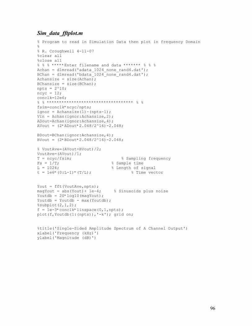
96
Sim_data_fftplot.m
% Program to read in Simulation Data then plot in frequency Domain % % R. Croughwell 4-11-07 %clear all %close all % % % *****Enter filename and data ******* % % % Achan = dlmread('adata_1024_none_rand4.dat'); BChan = dlmread('bdata_1024_none_rand4.dat'); Achansize = size(Achan); BChansize = size(BChan); npts = 2^10; ncyc = 12; conclk=12e6; % % *********************************** % % fsim=conclk*ncyc/npts; ignor = Achansize(1)-(npts-1); Vin = Achan(ignor:Achansize,2); ADout=Achan(ignor:Achansize,4); AVout = (2*ADout*2.048/2^16)-2.048; BDout=BChan(ignor:Achansize,4); BVout = (2*BDout*2.048/2^16)-2.048; % VoutAve=(AVout+BVout)/2; VoutAve=(AVout)/1; T = ncyc/fsim; % Sampling frequency Fs = 1/T; % Sample time L = 1024; % Length of signal t = 1e6*(0:L-1)*(T/L); % Time vector Yout = fft(VoutAve,npts); magYout = abs(Yout)+ 1e-4; % Sinusoids plus noise Youtdb = 20*log10(magYout); Youtdb = Youtdb - max(Youtdb); %subplot(2,1,2); f = 1e-3*conclk*linspace(0,1,npts); plot(f,Youtdb(1:(npts)),'-k'); grid on; %title('Single-Sided Amplitude Spectrum of A Channel Output') xlabel('Frequency (kHz)') ylabel('Magnitude (dB)')

97
Appendix D
NSF Proposal
Dr. John A. McNeill
Worcester Polytechnic Institute
Project Description
Introduction
This intent of the work described in this proposal is to continue development of a new
class of self-calibrating analog-to-digital converters (ADCs). The new "Split ADC"
architecture [D1] is specifically tailored to the constraints of advanced digital CMOS
processing technology. The capability of providing high resolution, self-calibrating
ADCs at low cost fills a critical need in a wide range of emerging mixed-signal
application areas.
This proposal is organized as follows: Section 1 describes the motivation for developing
the new ADC architecture, including application areas, performance requirements, and an
overview of previous ADC architectures and self calibration techniques.
Section 2 describes the P.I.'s previous work in developing the split ADC architecture,
which has been proven by successful fabrication and test of a 16bit, 1MSample/s, cyclic
ADC. Although the cyclic is not a widely used type of ADC, it was chosen as a low-risk
first step to investigate since only a single parameter need be estimated for self-
calibration.
Section 3 describes the proposed work: extension of the architecture concept to more
widely used types of ADCs: pipeline, successive approximation, and interleaved. This is
a higher-risk effort; in each case the self-calibration process is more complicated since
many parameters must be estimated. However, the higher risk is accompanied by a
higher reward due to the large number of application areas that will benefit. Section 4
concludes the proposal by summarizing the benefits expected from completion of the
proposed work.
1 Motivation
1.1 Applications

98
Scaling of CMOS integrated circuit (IC) technology into deep submicron (DSM) gate
dimensions has enabled dramatic improvement in cost, performance, and levels of system
integration. Scaling is especially beneficial for digital processing; the cost per function in
terms of die area and power has improved by approximately two orders of magnitude
every decade since 1970 [D2]. For analog functions, scaling can be a mixed blessing:
cost is improved due to reduced die area but analog performance is often degraded [D3].
Despite the performance challenges, the cost advantages of integrating systems in DSM
CMOS have motivated a wide variety of work in analog and mixed signal design.
One example is the wide variety of new mixed signal integrated circuit applications that
are enabled by the combination of DSM CMOS and integrated sensors. A simplified
version of an integrated sensor system is shown in Figure 1. Although these functions
may be realized on a "stand-alone" basis, it is increasingly likely that the entire functional
block performs as a subsystem in a larger network. In any case, the goal is to integrate
the entire system on a single IC to exploit the cost and integration advantages of DSM
CMOS. At the input a sensor, specific to the physical system, translates the signal to
analog form. Although the sensor electronics may provide some simple signal
conditioning (e.g. amplification), for many reasons it is advantageous to perform as much
processing in the digital domain as possible. Therefore, the function of the analog-to-
digital converter is to provide a digital representation of the analog signal for further
processing (e.g. filtering, signal detection) and communication.
Improvements in speed and accuracy of the ADC usually translate directly into improved
system-level performance. For example, in a CAT scan medical imaging application,
improved ADC accuracy can provide the capability for maintaining image quality while
reducing the X-ray dose received by the patient, or alternatively improving image quality
at a given radiation dose.
SENSOR
ANALOG TO
DIGITAL CONVERTER
DIGITAL PROCESSING
PHYSICAL SYSTEM BIOLOGICAL CHEMICAL MECHANICAL OPTICAL RADIOLOGICAL
ANALOG DIGITAL
INTEGRATED SYSTEM
Figure D1. Typical integrated sensor system.
A brief survey of recent work on integrated sensor systems shows a wide variety of
applications in areas such as:
• Correlated sensor networks [D4] used to detect terrorism threats from chemical,
biological, or nuclear weapons

99
• Pervasive sensing and actuation networks [D5] for use in monitoring and controlling
mechanical and ecological systems
• Monitoring for a wide range of environment toxins such as lead [D6], carbon
monoxide [D7], and industrial pollutants [D8]
• Implantable sensors for monitoring biosignals [D9]
• DNA detection [D10] for biological assay applications
• Biosensing of electrochemical signals [D11] for molecular biology applications
• Implanted sensing and actuating devices [D12] for assistive technology applications
A common theme running through this diversity of applications is the requirement for a
high resolution analog to digital conversion function. The key contribution of the
proposed work is that the ADC architecture that will be developed takes advantage of
CMOS scaling to enable reduced size, power, and cost for integrated systems in all of
these applications.
The following sections provide an overview of present ADC technology and describe the
difficulties with existing techniques that are overcome with the proposed architecture.1.2
ADC overview
As described in [D13, D14] ADCs can be broadly classified into Nyquist-rate and
oversampling converters. Since this proposal targets Nyquist-rate ADCs, the purpose of
this section is to contrast the two types of converters, show the importance of Nyquist-
rate converters, and give an indication of the broad range of applications which will
benefit from the performance improvement offered by the split ADC architecture.
1.1.1 Oversampling ADCs
Oversampling converters are well suited to submicron CMOS since oversampling allows
complexity and performance demands to be moved into the digital domain. The tradeoff
relaxes requirements on precision in the analog domain circuitry, and recovers precision
through extensive digital filtering. The prevalent oversampling converter architecture is
the Sigma-Delta [D13], which is widely used in high resolution applications such as
audio. However, oversampling ADCs show performance characteristics associated with
the use of digital filtering that can be significant disadvantages in some applications:
• There is significant latency (delay) in the output samples related to the length of the digital filter used, and
• Depending on the response of the digital filter, there may not be a one-to-one correspondence between the output samples and a time-domain representation of the
input signal.
For signals which are continuous in time, or for which the information content exists
entirely in the frequency domain, these characteristics are not disadvantageous.

100
1.1.2 Nyquist-Rate ADCs
Although oversampling techniques are advantageous in some cases, there are also many
applications for which oversampling techniques are unsuitable:
• Applications involving signals which are discontinuous in time; for example, multiplexed sensor signals
• Applications for which latency is critical; for example, signals inside closed loop control systems, in which delay leads to poor phase margin and instability
• Applications in which signal information is contained in the time domain and a one-to-one correspondence between input and output samples is required
• Applications with high bandwidth signals for which large oversampling ratios are either impossible or impractical due to high power requirements for circuitry operating
at the high oversampling speed.
Each of these classes of applications is better served by Nyquist-rate converters, which
provide the advantages of lower latency, one-to-one correspondence of input-output
samples, and reduced requirement on sampling speed. Within the class of Nyquist-rate
ADCs, there are many different architectures available with the choice depending on the
system-level tradeoffs of resolution, speed, and power.
Three widely used types of Nyquist-rate ADCs which could benefit from application of
the split ADC architecture are:
• Interleaved (suitable for higher speed applications; targeted by this proposal)
• Successive approximation (suitable for higher resolution applications)
• Pipeline (compromise offering high speed and high resolution)
A difficulty with design of Nyquist-rate converters is that until recently it has been
difficult to take advantage of CMOS scaling by moving complexity into the digital
domain; it has been necessary to maintain precise operation in the analog domain. For
the high resolution (>16 bit) applications targeted in this proposal, the inherent matching
available in CMOS analog circuitry is insufficient and some form of calibration is
necessary. These issues are discussed further in the following section, which describes
desired requirements for ADCs and calibration techniques in submicron CMOS.
1.2 Desired Characteristics for ADCs in Submicron CMOS
One-time factory calibration is common, but has the disadvantages of requiring expensive
test time. Additionally, since the calibration is fixed it cannot track variations due to
environmental and aging factors. For best utilization of the capabilities of submicron
CMOS, the ADC should be self-calibrating. Ideally the calibration procedure should
meet the following three criteria:
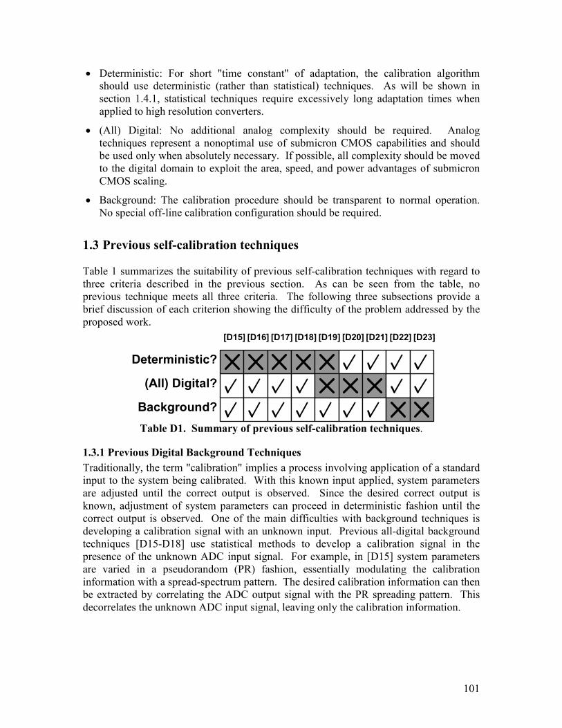
101
• Deterministic: For short "time constant" of adaptation, the calibration algorithm should use deterministic (rather than statistical) techniques. As will be shown in
section 1.4.1, statistical techniques require excessively long adaptation times when
applied to high resolution converters.
• (All) Digital: No additional analog complexity should be required. Analog techniques represent a nonoptimal use of submicron CMOS capabilities and should
be used only when absolutely necessary. If possible, all complexity should be moved
to the digital domain to exploit the area, speed, and power advantages of submicron
CMOS scaling.
• Background: The calibration procedure should be transparent to normal operation. No special off-line calibration configuration should be required.
1.3 Previous self-calibration techniques
Table 1 summarizes the suitability of previous self-calibration techniques with regard to
three criteria described in the previous section. As can be seen from the table, no
previous technique meets all three criteria. The following three subsections provide a
brief discussion of each criterion showing the difficulty of the problem addressed by the
proposed work.
[D15]
Deterministic?
(All) Digital?
Background?
[D16] [D17] [D18] [D19] [D20] [D21] [D22] [D23]
Table D1. Summary of previous self-calibration techniques.
1.3.1 Previous Digital Background Techniques
Traditionally, the term "calibration" implies a process involving application of a standard
input to the system being calibrated. With this known input applied, system parameters
are adjusted until the correct output is observed. Since the desired correct output is
known, adjustment of system parameters can proceed in deterministic fashion until the
correct output is observed. One of the main difficulties with background techniques is
developing a calibration signal with an unknown input. Previous all-digital background
techniques [D15-D18] use statistical methods to develop a calibration signal in the
presence of the unknown ADC input signal. For example, in [D15] system parameters
are varied in a pseudorandom (PR) fashion, essentially modulating the calibration
information with a spread-spectrum pattern. The desired calibration information can then
be extracted by correlating the ADC output signal with the PR spreading pattern. This
decorrelates the unknown ADC input signal, leaving only the calibration information.

102
N
CONVERSIONS REQUIRED FOR CALIBRATION
12 14 16
BITS RESOLUTION
104
105
106
107
108
109
22N
CYCLIC SPLIT ADC [1]
[D15] Galton2000 [D16] Murmann2003 [D17] Liu2004 [D18] Nair2004
[D19] Ryu2004
D16 D15
D18 D17
D19
Figure D2. Conversions required for calibration vs ADC resolution.
A critical difficulty with statistical approaches for high resolution ADCs is that extracting
calibration information to N-bit accuracy requires approximately 22N conversions. This
can be seen in Figure 2. For ADCs of high speed and moderate resolution this is
adequate; for example, the procedure in [D16] requires 224 conversions and about 300ms
for a 12b 75MS/s ADC. However higher resolution converters have been reported as
requiring excessively long calibration times of seconds or minutes [D17-D19].
Since statistical techniques require of order 22N conversions, these methods do not fulfill
the required characteristic of short calibration time. In contrast, the "split ADC"
architecture presented in [D1] enables a deterministic digital calibration procedure,
operating continuously in the background, which as shown in Figure 2 requires only
about 10,000 conversions to complete calibration. Thus the split ADC allows self-
calibration of high resolution ADCs at time scales short enough to track out the effects of
environmental variations such as temperature.
1.3.2 Previous Deterministic Background Techniques
Previous work to avoid the shortcomings of statistical techniques have involved added
analog complexity. One approach [D20] is queue-based, in which an additional sample-
and-hold (S/H) stage, operated at a higher sampling rate, is used to insert a known signal
for calibration. When the inserted known input is converted, the ADC output is
compared to the expected known value and a deterministic algorithm can be used to
rapidly calibrate the ADC. Another approach involves adding a slow-but-accurate ADC
in parallel with the ADC being calibrated [D21]. The slow-but-accurate ADC provides
an accurate value for a subset of the output values for the ADC being calibrated.
Unfortunately, these techniques do not fulfill the required characteristic of minimizing
analog complexity. In each case the additional analog circuitry imposes die area and
power penalties.

103
In contrast, the "split ADC" architecture requires no additional analog circuitry; the
system complexity is pushed to the digital side. This is the preferred tradeoff in
submicron CMOS, and has a relatively slight impact on overall die area
1.3.3 Previous Deterministic Digital Techniques
Previous deterministic digital techniques [D22, D23] take the converter off-line to
substitute a known signal for the input. This avoids the statistical problems associated
with calibrating in the presence of an unknown input, and allows rapid determination of
calibration parameters.
Unfortunately, since the ADC is off-line during calibration, these methods do not fulfill
the required characteristic of background operation. As will be described in Section 2,
the calibration process for the split ADC architecture operates entirely in the background.
2 New "Split ADC" Architecture
Subsection 2.1 describes the general idea of the split ADC architecture, independent of
any specific type of ADC. It is shown how the general idea fulfills the requirements of
all-digital, deterministic, background self-calibration.
2.1 General Split ADC Architecture
The architecture is shown in Figure 3. The ADC is split into two channels, each
converting the same input and producing individual output codes xA and xB. The average
of the two outputs is the ADC output code x. The background calibration signal is
developed from the difference ∆x between codes xA and xB and is completely transparent
to converter operation in the output code signal path. If both ADCs are correctly
calibrated, the two outputs will agree and the difference ∆x will be zero. In the presence
of nonzero differences, the pattern of "disagreements" in ∆x can be examined in an error
estimation process to adjust calibration parameters in each ADC, driving the difference
and the ADC errors to zero.

104
ADC "A"xA
vIN
xB
ERROR
ESTIMATION
+
+
+
-
x ====xA ++++ xB2
∆∆∆∆x ==== xB −−−− xA
ADC OUTPUT CODE
DIFFERENCE
ADC "B"
Figure D3. Split ADC Architecture.
Comparison with statistical techniques shows the advantage of using the difference ∆x
for the calibration signal. For example, both [D15] and [D16] use pseudorandom (PR)
sequences to decorrelate the calibration information from the unknown signal at the ADC
input, thus requiring a large number of conversions. In contrast, for the split ADC
approach the difference operation removes the unknown ADC input signal from the
calibration signal path. Thus it is no decorrelation is necessary and the number of
conversions required is greatly reduced, as was shown in Figure 2.
C gm
σσσσ x ==== nkT
C
fT ==== bgm
C
P ==== p ⋅⋅⋅⋅ gm
A
ANALOG DIGITAL
C
2
gm2
BC
2
gm2
xA
xB
vINx
ANALOG DIGITAL
vIN
SPLIT
Speed
Power
Noiseσσσσ x ====
1
2n
kT
C 2
2
++++1
2n
kT
C 2
2
==== nkT
C
fT ==== bgm 2
C 2
==== b
gm
C
P ==== p ⋅⋅⋅⋅gm
2++++ p ⋅⋅⋅⋅
gm
2==== p ⋅⋅⋅⋅ gm
xA ++++ xB2
x
Figure D4. Die Area, Speed, Power Consumption, Noise Considerations.
Figure 4 shows that this technique has negligible impact on analog complexity and
performance. The die area of an ADC designed to meet a given specification is
considered in simplified fashion as a gm block representing the area of active analog
circuitry such as amplifiers; a C block representing the area of passive components such

105
as capacitors and switches, and a digital circuitry block. It is assumed that bandwidth fT
is proportional to gm/C; power P is proportional to gm; and noise σX is proportional to kT C Proportionality constants b, p, and m are determined by the specific circuit
design and are unchanged by the split, which merely scales the design by 1/2. The
equations in the figure show that power, bandwidth, and overall noise are unchanged.
The only penalty is a slight increase in complexity of the digital block.
2.2 Specific Implementation: Cyclic ADC
As a first implementation of the split ADC concept, a cyclic (also called algorithmic)
ADC was chosen for simplicity in both analog complexity and calibration [D1]. The
analog circuitry required is simple, since the only critical analog block is a single gain
stage. The digital calibration is also relatively simple since the only parameter needed to
calibrate ADC linearity is the gain of the analog stage [D1].
A simplified system block diagram is shown in Figure 5. The analog portion of each
cyclic ADC consists of a S/H, a 16-bit-linear gain block (nominal gains GA=GB=1.92),
comparators, and a three-level DAC. To achieve 16-bit linear operation, a two-stage op-
amp with gain-boosted cascoding of the first stage was used. Fully differential
techniques were used with a standard switched-capacitor implementation of the S/H,
DAC, and gain stage. The output of the analog subsystem is a three-level (–1/0/+1)
decision for each cycle of the conversion process. For each side of the split, digital
outputs xA and xB are accumulated from the comparator decisions using a lookup table
(L.U.T.) containing the cycle decision weights, which are calculated from the gain
estimates ˆ G A and ˆ G B .

106
Figure D5. Cyclic ADC block diagram.
The background calibration process, indicated by the thick gray line in Figure 5, operates
continuously in the digital domain so that ˆ G A , ˆ G B and their associated L.U.T.s are
correct to within converter accuracy. The process begins with ˆ ε A and ˆ ε B , which are continuously updated zero-bias estimates of the error in the estimated gains ˆ G A and
ˆ G B .
Estimates ˆ ε A and ˆ ε B are used in an LMS procedure to update ˆ G A and ˆ G B ; as these are periodically updated, the decision weight L.U.T. is recalculated. The LMS coefficient µ
controls the time constant of the calibration adaptation and is subject to a tradeoff
between accuracy and speed of adaptation. The value of µ was chosen to give a time
constant of approximately 2,000 conversions; convergence from typical initial error is
completed within about 10,000 conversions.
It should be noted that the split ADC concept alone is not sufficient for error estimation.
Although accurate calibration does imply agreement in the output codes, it is not
necessarily true that agreement implies accurate calibration. Suppose that both A and B
sides of the split have the same error and make the same comparator decisions. Then
their output codes would agree even though the ADC code would be incorrect, and the
resulting ∆x=0 would provide no information to the error estimation process. To ensure
nonzero ∆x even if both ADCs have the same error, it is necessary to force the two sides
to take different decision paths to the final result of their conversions. Variation of the decision paths is achieved using the multiple residue mode cyclic amplifier [D1] which

107
combines aspects of the dual residue approach used in [D16] and the 1.5 bit/stage
amplifier in [D22].
As shown in Figure 5, estimation of ˆ ε A and ˆ ε B requires coefficients SDKA and SDKB, which are accumulated for each conversion using the decisions and an error coefficient
L.U.T. In principle, εA and εB could be estimated by solving a 2x2 matrix equation using SDKA and SDKB values from only two conversions. In practice, to simplify digital
hardware and average out the effects of random noise in ∆x, an iterative procedure is
used to develop ˆ ε A and ˆ ε B over several conversions. An additional benefit of manipulating the different residue modes should also be noted: coefficients SDKA,
SDKB, and the ∆x signal are modulated with sufficient activity that a "busy" ADC input
signal is not required to extract calibration information.
Figure D6. INL Plots Figure 7. Die Photo
Figure 6 shows measured INL errors with and without calibration. Disabling calibration
and operating with the default initial value L.U.T.s (calculated from the nominal gain of
1.92) gives INL error of ≈ ±25LSB. With calibration enabled, INL error improves to
+2.1/-4.8 LSB. Figure 7 shows the die photo. The analog portion of the ADC was
fabricated on a 1P4M 0.25µm digital CMOS process with deep N-well. Area is 1.16mm
x 1.38mm for the analog; the digital circuitry was implemented on an external FPGA
which would have synthesized to 1.5mm2 in the 0.25µm CMOS process. Power
consumption for the analog is 105mW from a 2.5V supply.

108
Figure D8. INL Plots vs. Temperature Figure D9. Measured Calibration
2.3 Measured Response to Environmental Variations
Due to the reduced number of conversions required, the continuous background
calibration means the ADC can track out changes in calibration parameters caused by
environmental changes such as temperature. This is shown in Figures 8 and 9. The top
plot in Figure 8 shows measured INL at +85°C. For the middle plot, calibration was
disabled, temperature was reduced to -40°C, and then INL was measured. Without the
background calibration operating, the 85°C parameters are incorrect at -40°C and the INL
plot shows degraded linearity. For the bottom plot, calibration was re-enabled; after a
convergence transient the original INL performance is measured when the calibration
coefficients have converged to the new values required for –40°C. Figure 9 shows a plot
of the gain estimate as a function of time, showing the acquisition transient of the
calibration. The response is a damped exponential; calibration is acquired to sufficient
accuracy within about 10,000 conversions.
2.4 Summary of Cyclic Converter Performance
The cyclic ADC described in this section proved the practical operation of the split ADC
concept as a way to achieve all of the desired calibration procedure characteristics. By
performing all calibration and correction in the digital domain, the technique successfully
moves complexity into the digital domain as desired, with no additional analog
complexity. The technique operates in the background, with no interruption of input
sampling. And unlike all previous digital background techniques, this technique is
deterministic rather than statistical. The calibration procedure converges in
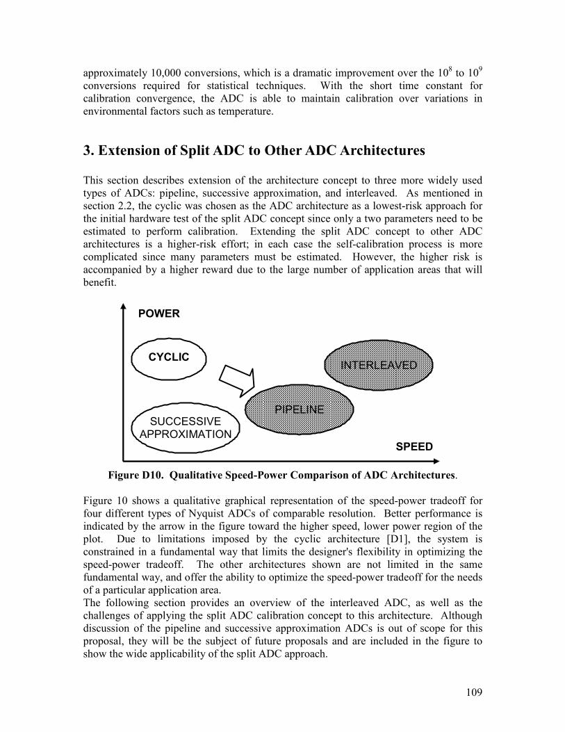
109
approximately 10,000 conversions, which is a dramatic improvement over the 108 to 10
9
conversions required for statistical techniques. With the short time constant for
calibration convergence, the ADC is able to maintain calibration over variations in
environmental factors such as temperature.
3. Extension of Split ADC to Other ADC Architectures
This section describes extension of the architecture concept to three more widely used
types of ADCs: pipeline, successive approximation, and interleaved. As mentioned in
section 2.2, the cyclic was chosen as the ADC architecture as a lowest-risk approach for
the initial hardware test of the split ADC concept since only a two parameters need to be
estimated to perform calibration. Extending the split ADC concept to other ADC
architectures is a higher-risk effort; in each case the self-calibration process is more
complicated since many parameters must be estimated. However, the higher risk is
accompanied by a higher reward due to the large number of application areas that will
benefit.
SPEED
POWER
CYCLIC
SUCCESSIVE APPROXIMATION
PIPELINE
INTERLEAVED
Figure D10. Qualitative Speed-Power Comparison of ADC Architectures.
Figure 10 shows a qualitative graphical representation of the speed-power tradeoff for
four different types of Nyquist ADCs of comparable resolution. Better performance is
indicated by the arrow in the figure toward the higher speed, lower power region of the
plot. Due to limitations imposed by the cyclic architecture [D1], the system is
constrained in a fundamental way that limits the designer's flexibility in optimizing the
speed-power tradeoff. The other architectures shown are not limited in the same
fundamental way, and offer the ability to optimize the speed-power tradeoff for the needs
of a particular application area.
The following section provides an overview of the interleaved ADC, as well as the
challenges of applying the split ADC calibration concept to this architecture. Although
discussion of the pipeline and successive approximation ADCs is out of scope for this
proposal, they will be the subject of future proposals and are included in the figure to
show the wide applicability of the split ADC approach.
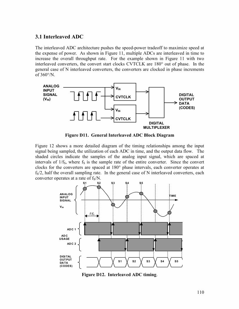
110
3.1 Interleaved ADC
The interleaved ADC architecture pushes the speed-power tradeoff to maximize speed at
the expense of power. As shown in Figure 11, multiple ADCs are interleaved in time to
increase the overall throughput rate. For the example shown in Figure 11 with two
interleaved converters, the convert start clocks CVTCLK are 180° out of phase. In the
general case of N interleaved converters, the converters are clocked in phase increments
of 360°/N.
ANALOGINPUTSIGNAL(VIN)
DIGITALOUTPUTDATA(CODES)
VIN
CVTCLK
VIN
CVTCLKDIGITAL
MULTIPLEXER
Figure D11. General Interleaved ADC Block Diagram
Figure 12 shows a more detailed diagram of the timing relationships among the input
signal being sampled, the utilization of each ADC in time, and the output data flow. The
shaded circles indicate the samples of the analog input signal, which are spaced at
intervals of 1/fS, where fS is the sample rate of the entire converter. Since the convert
clocks for the converters are spaced at 180° phase intervals, each converter operates at
fS/2, half the overall sampling rate. In the general case of N interleaved converters, each
converter operates at a rate of fS/N.
TIMEANALOGINPUTSIGNAL
VIN
S1 S2 S3 S4 S5
S1 S2 S3 S4 S5
DIGI TALOUTPUTDATA(CODES)
ADCUSAGE
ADC 1
ADC 2
1/fS
Figure D12. Interleaved ADC timing.
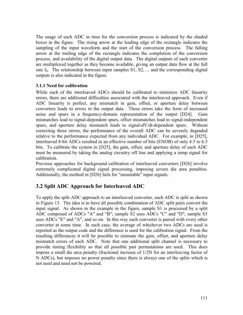
111
The usage of each ADC in time for the conversion process is indicated by the shaded
boxes in the figure. The rising arrow at the leading edge of the rectangle indicates the
sampling of the input waveform and the start of the conversion process. The falling
arrow at the trailing edge of the rectangle indicates the completion of the conversion
process, and availability of the digital output data. The digital outputs of each converter
are multiplexed together as they become available, giving an output data flow at the full
rate fS. The relationship between input samples S1, S2, ... and the corresponding digital
outputs is also indicated in the figure.
3.1.1 Need for calibration
While each of the interleaved ADCs should be calibrated to minimize ADC linearity
errors, there are additional difficulties associated with the interleaved approach. Even if
ADC linearity is perfect, any mismatch in gain, offset, or aperture delay between
converters leads to errors in the output data. These errors take the form of increased
noise and spurs in a frequency-domain representation of the output [D24]. Gain
mismatches lead to signal-dependent spurs, offset mismatches lead to signal-independent
spurs, and aperture delay mismatch leads to signal-dV/dt-dependent spurs. Without
correcting these errors, the performance of the overall ADC can be severely degraded
relative to the performance expected from any individual ADC. For example, in [D25],
interleaved 8-bit ADCs resulted in an effective number of bits (ENOB) of only 4.5 to 6.5
bits. To calibrate the system in [D25], the gain, offset, and aperture delay of each ADC
must be measured by taking the analog circuitry off line and applying a ramp signal for
calibration.
Previous approaches for background calibration of interleaved converters [D26] involve
extremely complicated digital signal processing, imposing severe die area penalties.
Additionally, the method in [D26] fails for "unsuitable" input signals.
3.2 Split ADC Approach for Interleaved ADC
To apply the split ADC approach to an interleaved converter, each ADC is split as shown
in Figure 13. The idea is to have all possible combination of ADC split pairs convert the
input signal. As shown in the example in the figure, sample S1 is processed by a split
ADC composed of ADCs "A" and "B"; sample S2 uses ADCs "C" and "D"; sample S3
uses ADCs "E" and "A", and so on. In this way each converter is paired with every other
converter at some time. In each case, the average of whichever two ADCs are used is
reported as the output code and the difference is used for the calibration signal. From the
resulting differences it will be possible to estimate the gain, offset, and aperture delay
mismatch errors of each ADC. Note that one additional split channel is necessary to
provide timing flexibility so that all possible pair permutations are used. This does
impose a small die area penalty (fractional increase of 1/2N for an interleaving factor of
N ADCs), but imposes no power penalty since there is always one of the splits which is
not used and need not be powered.
112
TIMEANALOGINPUTSIGNAL
VIN
S1 S2 S3 S4 S5
S1 S2 S3 S4 S5
DIGITALOUTPUTDATA(CODES)
ADCUSAGE
ADC "A"
1/fS
ADC "B"
ADC "C"
ADC "D"
ADC "E"
Figure D13. Split ADC Approach applied to Interleaved ADCs
3.2.1 Challenges for Split ADC Calibration of Interleaved ADCs
The main difficulty for the split ADC approach in the case of interleaved converters is the
increased number of parameters that need to be estimated. For an interleaving factor of
N, the split ADC approach requires estimation of gain, offset, and aperture delay for each
of (2N+1) converters, for a total of 3(2N+1) parameters to be estimated. In the case of
the N=2 interleaving shown in Figure 13, a total of 15 parameters are necessary, which is
a dramatic increase from the two parameter estimation demonstrated in the cyclic case. If
split ADC techniques are also used to correct for linearity errors in each individual ADC,
the number of parameters to be estimated increases further.
3.3. Proposed Work
The centerpiece of the proposed work is the design, fabrication, and test of a prototype
integrated circuit to verify the embodiment of the “Split ADC” concept in an interleaved
ADC of the general form described in section 3.2. The project would be performed by a
full-time Ph.D. student under the direction of the P.I. Figure 14 provides an overview of
the major tasks in the proposed work, and their approximate scheduling over the project
duration of three years. Given the P.I.’s past experience advising graduate research at
WPI (See Biographical Sketch), the amount of time budgeted – full time for the Ph.D.
student and one summer month per year for the P.I. – are appropriate given the nature of
the proposed work

113
Figure D14. Schedule of proposed work. Task
Survey existing technology;
determine target specification
System level design;
behavioral modeling
Circuit level design of
prototype IC
IC fabrication
Test system design
Test system fabrication
Integration of prototype IC,
test system
Test and verification of
prototype IC in test system
Dissemination of results
YEAR 1 YEAR 2 YEAR 3
4. Benefits
It is the P.I.’s belief that the new "Split ADC" architecture represents a genuine creative
design breakthrough in response to the specific constraints of advanced digital CMOS
processing technology. The capability of providing high resolution, self-calibrating
ADCs at low cost fills a critical need in a wide range of emerging mixed-signal
application areas. Successful completion of the work described in this proposal will
extend development of this new class of self-calibrating analog-to-digital converters
(ADCs) to the important application area of interleaved ADCs.
The P.I.'s previous work in developing the "split ADC" architecture has been proven by
successful fabrication and test of a 16bit, 1MSample/s, cyclic ADC. This is an indication
of both the validity of the concept to be extended and the P.I.’s ability to successfully
complete the proposed work.

114
References for NSF Proposal
[D1] J. McNeill, M. Coln, and B. Larivee, "A Split-ADC Architecture for Deterministic
Digital Background Calibration of a 16b 1MS/s ADC," International Solid-State
Circuits Conference (ISSCC) Digest of Technical Papers, February, 2005, pp. 276-
7.
[D2] G. Moore, "No exponential is forever, but forever can be delayed," International
Solid-State Circuits Conference (ISSCC) Digest of Technical Papers, February,
2003, pp. 20-23.
[D3] B. Razavi, "CMOS technology characterization for analog and RF design," IEEE
Journal of Solid-State Circuits, vol. 34 , no. 3 , March 1999, pp. 268 - 276
[D4] R. Hills, "Sensing for Danger," Science and Technology Review, July/August, 2001,
pp. 11-17.
[D5] D. Estrin et al., "Instrumenting the world with wireless sensor networks,"
Proceedings of the 2001 IEEE International Conference on Acoustics, Speech, and
Signal Processing (ICASSP '01), May, 2001, pp. 2033 - 2036.
[D6] S. Martin, F. Gebara, B. Larivee, and R. Brown, "A Microsystem for Trace
Environmental Monitoring," International Solid-State Circuits Conference (ISSCC)
Digest of Technical Papers, February, 2005, pp. 244-5.
[D7] A. Burresi et al., "Temperature profile investigation of SnO2 sensors for CO
detection enhancement," IEEE Transactions on Instrumentation and
Measurement, vol. 54, no. 1, February, 2005, pp. 79-86.
[D8] P. Arpaia et al., "A chloroform transducer based on sPS-d-coated quartz-crystal
microbalance for gaseous environment," IEEE Transactions on Instrumentation and
Measurement, vol. 54, no. 1, February, 2005, pp. 31-37.
[D9] R. Beach et al., "Towards a miniature implantable in vivo telemetry monitoring
system dynamically configurable as a potentiostat or galvanostat for two- and three-
electrode biosensors," IEEE Transactions on Instrumentation and Measurement,
vol. 54, no. 1, February, 2005, pp. 61-72.
[D10] Y. Yazawa et al., "A Wireless Biosensing Chip for DNA Detection,"
International Solid-State Circuits Conference (ISSCC) Digest of Technical Papers,
February, 2005, pp. 562-3.
[D11] A. Hassibi and T. Lee, "A Programmable Electrochemical Biosensor Array in
0.18µm Standard CMOS," International Solid-State Circuits Conference (ISSCC)
Digest of Technical Papers, February, 2005, pp. 564-5.
[D12] P. R. Kennedy et al., "Computer Control Using Human Intracortical Local Field
Potentials," IEEE Transactions on Neural Systems and Rehabilitation Engineering,
vol. 12, no. 3, September, 2004, pp. 339-344.
115
[D13] D. Johns and K. Martin, "Analog Integrated Circuit Design." John Wiley & Sons,
New York, 1997.
[D14] Analog Devices Technical Staff, "Analog-Digital Conversion Handbook."
Prentice-Hall, New Jersey, 1997.
[D15] I. Galton, "Digital cancellation of D/A converter noise in pipelined ADCs," IEEE
Transactions on Circuits and Systems II: Analog and Digital Signal Processing,
March 2000, pp. 185-196.
[D16] B. Murmann et al., "A 12b 75MS/s Pipelined ADC using open-loop residue
amplification," International Solid-State Circuits Conference (ISSCC) Digest of
Technical Papers, February, 2003, pp. 328-9.
[D17] Liu et al, "A 15b 20MS/s CMOS Pipelined ADC with Digital Background
Calibration," International Solid-State Circuits Conference (ISSCC) Digest of
Technical Papers, February, 2004, pp. 454-5.
[D18] Nair et al., "A 96dB SFDR 50MS/s Digitally Enhanced CMOS Pipelined A/D
Converter," International Solid-State Circuits Conference (ISSCC) Digest of
Technical Papers, February, 2004, pp. 456-7.
[D19] Ryu et al., "A 14b-Linear Capacitor Self-Trimming Pipelined ADC,"
International Solid-State Circuits Conference (ISSCC) Digest of Technical Papers,
February, 2004, pp. 464-5.
[D20] Erdogan et al., "A 12-b Digital-Background-Calibrated Algorithmic ADC with -
90-dB THD," International Solid-State Circuits Conference (ISSCC) Digest of
Technical Papers, February, 1999, pp. 316-7.
[D21] Chiu et al., "Least mean square adaptive digital background calibration of
pipelined ADCs," IEEE Transactions on Circuits and Systems I: Fundamental
Theory and Applications, Jan. 2004.
[D22] H.-S. Lee, "A 12-b 600 ks/s digitally self-calibrated pipelined algorithmic ADC,"
IEEE Journal of Solid-State Circuits, Apr. 1994, pp. 509 -515
[D23] A. Karanicolas et al. , "A 15-b 1-MS/s digitally self-calibrated pipeline ADC,"
IEEE Journal of Solid-State Circuits, Dec. 1993, pp. 1207 -1215
[D24] M. Looney, "Advanced Digital Post-Processing Techniques Enhance Performance
in Time-Interleaved ADC Systems," Analog Dialogue, vol. 37, no. 8, August, 2003.
[D25] K. Poulton et al., "A 20GS/s 8b ADC with a 1MB memory in 0.18µm CMOS,"
International Solid-State Circuits Conference (ISSCC) Digest of Technical Papers,
February, 2003, pp. 318-319.
[D26] S. Jamal et al., "Calibration of sample-time error in a two-channel time-
interleaved analog-to-digital converter," IEEE Transactions on Circuits and
Systems I: Fundamental Theory and Applications, vol. 51, no. 1 , January, 2004, pp.
130 - 139.