a 160-mhz bandwidth wireless signal tester - ti. · pdf fileup to 64-qam wi-fi a/c (ieee...
TRANSCRIPT
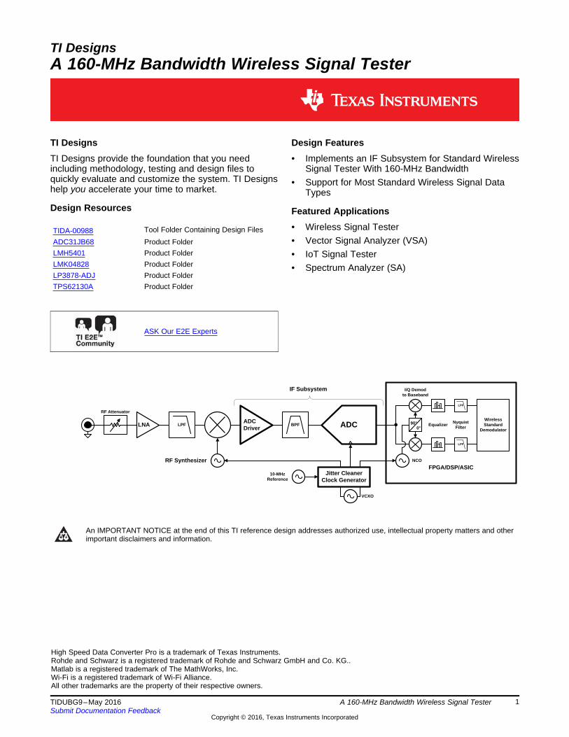
FPGA/DSP/ASIC
ADC 0° 90°
LPF
LPF
NyquistFilter
Equalizer
I/Q Demodto Baseband
WirelessStandard
Demodulator
Jitter CleanerClock Generator
NCO
BPF ADC Driver
LPF LNA
RF Attenuator
10-MHz Reference
VCXO
RF Synthesizer
IF Subsystem
1TIDUBG9–May 2016Submit Documentation Feedback
Copyright © 2016, Texas Instruments Incorporated
A 160-MHz Bandwidth Wireless Signal Tester
TI DesignsA 160-MHz Bandwidth Wireless Signal Tester
High Speed Data Converter Pro is a trademark of Texas Instruments.Rohde and Schwarz is a registered trademark of Rohde and Schwarz GmbH and Co. KG..Matlab is a registered trademark of The MathWorks, Inc.Wi-Fi is a registered trademark of Wi-Fi Alliance.All other trademarks are the property of their respective owners.
TI DesignsTI Designs provide the foundation that you needincluding methodology, testing and design files toquickly evaluate and customize the system. TI Designshelp you accelerate your time to market.
Design Resources
TIDA-00988 Tool Folder Containing Design FilesADC31JB68 Product FolderLMH5401 Product FolderLMK04828 Product FolderLP3878-ADJ Product FolderTPS62130A Product Folder
ASK Our E2E Experts
Design Features• Implements an IF Subsystem for Standard Wireless
Signal Tester With 160-MHz Bandwidth• Support for Most Standard Wireless Signal Data
Types
Featured Applications• Wireless Signal Tester• Vector Signal Analyzer (VSA)• IoT Signal Tester• Spectrum Analyzer (SA)
An IMPORTANT NOTICE at the end of this TI reference design addresses authorized use, intellectual property matters and otherimportant disclaimers and information.
System Description www.ti.com
2 TIDUBG9–May 2016Submit Documentation Feedback
Copyright © 2016, Texas Instruments Incorporated
A 160-MHz Bandwidth Wireless Signal Tester
1 System DescriptionThis reference design implements an IF subsystem for a standard wireless signal tester with an activebalun-amplifier (LMH5401), LC bandpass filter, and 16-bit ADC (ADC31JB68). Measurements usingmodulated signals demonstrate reception of the signal with high constellation clarity and MER sufficient fortesting a wide variety of standard signal types.
2 MotivationThe ability of a RF front-end receiver of a wireless signal tester to reliably measure and characterize asignal is constrained by a number of performance aspects, notably the available demodulation bandwidth,third-order inter-modulation distortion (IMD3), noise spectral density, and phase noise. The bandwidthmust accommodate the supported standards with the widest channel, while the noise and distortion mustbe order(s) of magnitude better than the performance of the Device Under Test (DUT).
Table 1 shows a survey summary of relevant characteristics from a variety of wireless standards. Earlystandards such as 802.11b, GSM or EDGE and the CDMA-based standards generally occupied less than25-MHz of bandwidth and used simple modulation schemes, mostly variations of QPSK. However, morerecent standards and multi-carrier use cases have driven the tester requirements to higher bandwidthsand better performance to support the higher order modulation schemes. Wi-Fi® (802.11 a/c) is animportant case that can transmit signals with up to 160 MHz of bandwidth and with a modulation order upto 256-QAM.
Table 1. Characteristics of Wireless Data Standards
STANDARD CARRIER FREQUENCY MODULATED CHANNELBANDWIDTH MODULATION
Wi-Fi B (IEEE 802.11b) 2.4 GHz 22 MHz Channel DSSS
Wi-Fi N (IEEE 802.11n) 2.5 and 5 GHz Channel up to 40 MHz OFDM, Subcarriersup to 64-QAM
Wi-Fi A/C (IEEE 802.11a/c) 5 GHz Channel up to 160 MHz OFDM, Subcarriersup to 256-QAM
WiMAX (IEEE 802.16) 2.3 GHz to 5.8 GHz Channel up to 20 MHz SOFDMA, Subcarriersup to 64-QAM
Bluetooth (IEEE 802.15) 2.4 GHz 1 MHz, Frequency hoppingacross 80 MHz
GFSK (BR), pi/4-DQPSK,8DPSK (EDR)
Zigbee (IEEE 802.15.4) 850 MHz, 815 MHz, 2,450MHz
Channel up to 2 MHz (5 MHzspacing) BPSK, OQPSK
UMTS FDD, WCDMA(3GPP) 0.7 GHz to 3.6 GHz Channel up to 5 MHz Multi-carrier
up to 80 MHzQPSK, DQPSKup to 64-QAM
LTE FDD (3GPP) 0.7 GHz to 3.6 GHz Channel up to 20 MHz Multi-carrierup to 80 MHz
OFDM SC-FMDAup to 64-QAM
GSM and EDGE 0.4 GHz to 1.9 GHz 200 kHz Channel Multi-carrierup to 75 MHz GMSK, 8PSK

N 2 2k 1 k k
Nkk 1
1I Q
EVMNMER 10 log10 20 log101 100%
eN
=
=
æ öå +ç ÷ æ ö
= ´ = - ´ç ÷ ç ÷è øç ÷åç ÷
è ø
N
kk 1
N 2 2
k kk 1
1e
NEVM 100%
1I Q
N
=
=
= ´
+
å
å
FPGA/DSP/ASIC
ADC 0° 90°
LPF
LPF
NyquistFilter
Equalizer
I/Q Demodto Baseband
WirelessStandard
Demodulator
Jitter CleanerClock Generator
NCO
BPF ADC Driver
LPF LNA
RF Attenuator
10-MHz Reference
VCXO
RF Synthesizer
IF Subsystem
www.ti.com Motivation
3TIDUBG9–May 2016Submit Documentation Feedback
Copyright © 2016, Texas Instruments Incorporated
A 160-MHz Bandwidth Wireless Signal Tester
Figure 1 shows the basic block diagram of a wireless signal tester receiver, also similar to a vector signalanalyzer (VSA). An LNA and RF attenuator condition the signal amplitude, a mixer down-converts thechannel (or band) to the intermediate frequency band, the IF subsystem filters and samples the signal,and a digital processor filters and demodulates the signal into symbols dictated by the modulationscheme. The performance of the system is limited by its ability to demodulate standard signals andquantified using popular performance metrics, such as the error vector magnitude (EVM) or ModulationError Ratio (MER).
Figure 1. Wireless Signal Tester Receiver Block Diagram
Typically, the demodulation MER performance of a wireless tester must be 10 dB better than theperformance requirements of the highest order modulation scheme for a given signal power level toadequately resolve the symbol constellation and quantify the EVM or MER of the unit under test. Here, thefollowing definitions are used for EVM and MER where N is the number of symbols captured, ek is themagnitude of the respective error vector, and Ik and Qk are the in-phase and quadrature components ofthe ideal respective symbol. This EVM definition is consistent with the 3GPP UMTS and LTE standards,and the MER definition is consistent with the ETSI Digital Video Broadcasting measurement guidelines.Both definitions are closely related. The equations for MER and EVM are shown in Equation 1 andEquation 2, respectively.
(1)
(2)
Higher order modulation schemes have more closely spaced constellations leading to a highersusceptibility to bit errors for a given MER or EVM value. Figure 2 shows the theoretical Symbol ErrorRate (SER) and EVM that corresponds to the given MER (modeled only with AWGN) for a variety ofquadrature amplitude modulation schemes.
A wideband 256-QAM signal test signal is a strenuous test case to determine the quality of the testersubsystem, including its functional dynamic range, minimum detectable signal (MDS), and inherent signalintegrity before passband equalization. Based on the MER performance requirements to achieveSER<10^–3 shown in Table 2, and assuming the tester's performance must be 10 dB better, the testermust resolve the signal with an MER of greater than 40 dB across a wide range of signal poweramplitudes.

Analog IF input
Power
Configuration 10-MHz clock reference
LMK04828
LC bandpass filter ADC31JB68LMH5401
ES/N0 Ratio (or MER) [dB]
Sym
bol E
rror
Rat
e (S
ER
)
0 5 10 15 20 25 30 35 401E-6
1E-5
1E-4
1E-3
1E-2
1E-1
1E+0QPSK16-QAM64-QAM256-QAM
System Description www.ti.com
4 TIDUBG9–May 2016Submit Documentation Feedback
Copyright © 2016, Texas Instruments Incorporated
A 160-MHz Bandwidth Wireless Signal Tester
Figure 2. Symbol Error Rate and EVM for a Given MER
Table 2. Theoretical MER and EVM Performance Requirements of Various Modulation Schemes
MODULATION MER REQUIREDfor 10^–3 SER
EVM REQUIREDfor 10^–3 SER
QPSK (4-QAM) 10 dB 30%16-QAM 18 dB 13%64-QAM 24 dB 6%256-QAM 30 dB 3.2%
3 System DescriptionThis reference design implements an IF subsystem for a standard wireless signal tester with an activebalun-amplifier (LMH5401), LC bandpass filter, 16-bit ADC (ADC31JB68) and clock cleaner and generatorPLL (LMK04828), as shown in Figure 3. Measurements using modulated signals demonstrate reception ofthe signal with high constellation clarity and MER sufficient for testing a wide variety of standard signaltypes.
Figure 3. Wideband Receiver Subsystem Reference Design

ADC31JB68 LMH5401
10-MHz Reference 100-MHz
VCXO
VIN+
VIN-V
CM
0.1 µF10 µF
10 µF
10 Q
150 �
CLK
IN+
CLK
IN-
25 � 174 �
36.5 �
36.5 �
0.1 µF
0.1 µF
0.1 µF
0.1 µF
174 �
137 �
36.5 �
÷ N
÷ R
÷
÷ N
÷ R
PF
D
PF
D ÷
÷
LMK04828 (PLL1+PLL2)
SY
SR
EF
+S
YS
RE
F-
÷
FM
C C
onne
ctor
500 MHz
15.625 MHz
250 MHz
15.625 MHz
LC Bandpass FilterCenter = 375 MHz
-1-dB BW = 160 MHz
5 Gbps
Optional External Clock
Reference
www.ti.com System Description
5TIDUBG9–May 2016Submit Documentation Feedback
Copyright © 2016, Texas Instruments Incorporated
A 160-MHz Bandwidth Wireless Signal Tester
3.1 ADC31JB68The ADC31JB68 is a 16-bit ADC sampling at 500 MSPS. The digital outputs are provided on twoJESD204B differential lanes, transmitting at 5 Gb per second per lane. The driver-to-ADC interface is ACcoupled, thus, the input common mode reference for the ADC is provided through the two 150-Ωtermination resistors at the ADC input.
3.2 LMH5401The LMH5401 is a wide-bandwidth, high-linearity, fixed-gain amplifier that performs a single-to-differentialsignal conversion. The external components around the amplifier are configured for a 12-dB voltage gainfrom the SMA connector input to the amplifier output and 50-Ω impedance into the SMA input connector.
3.3 LMK04828The LMK04828 is a dual-PLL jitter cleaner and clock generator. An on-board 10-MHz reference oscillator(or external signal) can provide the PLL1 input reference, a 100MHz VCXO is used as the VCO of PLL1,and the loop filter bandwidth is set very low to filter the clock noise. PLL2 multiplies the frequency up toapproximately 3 GHz and divides down to synthesize the necessary clocks. The ADC is a JESD204Bdevice, so both device clocks and SYSREF clocks are provided to the ADC and to the connector to beused by the downstream signal processor.
4 Block DiagramFigure 4 shows the TSW31JB68 EVM block diagram.
Figure 4. TSW31JB68EVM Block Diagram

Analog Input
Analog InputLow Noise
Signal Generator
Mini-USB Cable
Mini-USBCable
5-V Power Supply
BandpassFilter
PC ComputerRunning HSDC Pro
and Matlab
+6 V
TSW14J56EVM
PowerSwitch
OFF ON
EX
TR
EF
6-V Power Supply
10-MHz ClockReference
Measurement Setup www.ti.com
6 TIDUBG9–May 2016Submit Documentation Feedback
Copyright © 2016, Texas Instruments Incorporated
A 160-MHz Bandwidth Wireless Signal Tester
5 Measurement SetupThe measurement test bench utilized a Rohde and Schwarz® SMU200A Vector Signal Generator (VSG) togenerate the modulated signals, a TSW14J56EVM data capture card to capture the data, the High SpeedData Converter Pro ™(HSDC Pro) software to perform spectral analysis, and Matlab® software to performdemodulation and EVM and MER analysis. Figure 5 shows the bench evaluation setup. Measurementsusing Continuous Wave (CW) signals used a similar test setup except that a Rohde & Schwarz SMA100ARF signal generator created the signal.
The VSG provided a macro routine for generating a multi-carrier WCDMA signal, as well as a customizedmodulated signal builder to create a 256-QAM signal with root-raised cosine filter (0.22) pulse shaping. Toensure optimal demodulation performance, the LMK04828 clock chip on the reference design was lockedto the 10-MHz clock reference from the SMU200A. The TSW14J56EVM captured data from theADC31JB68 over a two-lane JESD204B serial data link operating at 5 Gb/s/ane, and delivered the data tothe computer. HSDC Pro was used to calculate channel power and peak-to-average ratio of themodulated signals. The 524k-sample data set was then exported to Matlab where it was signal processedto apply the I/Q demodulation to baseband, matched root-raised cosine (alpha= 0.22) filter, and symbolslicer (decimation). De-spreading (code correlation) of the WCMDA signals was not performed so theconstellations show the raw QPSK data stream performance and MER is specified before the de-spreading gain.
Figure 5. Bench Evaluation Setup

Input Frequency [MHz]
SN
R, S
INA
D [d
BF
S]
NS
D [d
BF
S/H
z]
250 300 350 400 450 50060 -155
61 -154
62 -153
63 -152
64 -151
65 -150
66 -149
67 -148
68 -147
69 -146
70 -145SNR [dBFS]SINAD [dBFS]NSD [dBFS/Hz]
Frequency [MHz]
Mag
nitu
de [d
BF
S]
0 100 200 300 400 500 600 700-20
-18
-16
-14
-12
-10
-8
-6
-4
-2
0
2
160 MHz
www.ti.com Measured Data
7TIDUBG9–May 2016Submit Documentation Feedback
Copyright © 2016, Texas Instruments Incorporated
A 160-MHz Bandwidth Wireless Signal Tester
6 Measured Data
6.1 SelectivityThe selectivity is determined by the LC bandpass filter. The chosen topology achieves a high order of roll-off on the upper transition band but sacrifices some unnecessary roll-off on the lower transition to achievebetter differential signal balance. The improved differential signal balance across component variationresults in better HD2 performance from the ADC. The filter has a 160 MHz -1 dB bandwidth and iscentered in the middle of the second Nyquist zone at 375 MHz, as shown in Figure 6. The worst caseHD2 occurs at 2×(375–160÷2)= 590 MHz which has approximately 20 dBc of typical suppression.
Figure 6. IF Subsystem Frequency Response
6.2 Noise PerformanceThe total gain of the subsystem is 7.1 dB at mid-band and the input (sinusoidal) power that corresponds toADC full scale is 1.5 dBm. With no input signal, the subsystem SNR is 70 dBFS, which corresponds to anoise spectral density (NSD) of –154 dBFS/Hz (–152.5 dBm/Hz) at the ADC output. The Noise Figure isapproximately 14.4 dB at the SMA connector input.
The SNR and NSD of the subsystem with a –1 dBFS CW tone is shown in Figure 7. The degradation inthe noise performance across frequency is due to the phase noise performance of the LMK04828 as wellas the additive jitter from the ADC. Based on the noise performance, the sensitivity and dynamic rangecan be calculated for various standard signals, as listed in Table 3. The 256-QAM, 20-MHz signal hasbeen included as an aggressive test case.
Figure 7. SNR, SINAD, and Noise Spectral Density vs Single-Tone Input Frequency

Input Amplitude [dBFS/tone]
Mag
nitu
de [d
BF
S]
-60 -50 -40 -30 -20 -10 0-120
-115
-110
-105
-100
-95
-90
-85
-80
-75
-70IMD3, 2F1 - F2IMD3, 2F2 - F1
Input Frequency [MHz]
Mag
nitu
de [d
BF
S]
250 300 350 400 450 50060
65
70
75
80
85
90
95
100
SFDR [dBFS]HD2 [dBFS]HD3 [dBFS]Next Spur [dBFS]
dB dB dBmDR 1.5 dBm 3 dB PAPR MDS= + - -
dBm dBm/Hz dB 10MDS NSD SNR 10 log (BW)= + + ´
Measured Data www.ti.com
8 TIDUBG9–May 2016Submit Documentation Feedback
Copyright © 2016, Texas Instruments Incorporated
A 160-MHz Bandwidth Wireless Signal Tester
Table 3. Subsystem Sensitivity and Dynamic Range for Various Standard Signals Based on Noise
SIGNAL TYPEREQUIRED BASEBAND
SNR (ES/N0) FORDEMODULATION 1
MINIMUMDETECTABLE
SIGNAL (MDS) 2
ASSUMEDSIGNAL PAPR
SUBSYSTEMDYNAMIC RANGE
LTE, 5MHz Carrier16-QAM CR=2/3 11.3 dB –74.2 dBm 10 dB Approximately 68.7 dB
WCDMA, 3.84MHzCarrier –18 dB 3 –103.5 dBm 11 dB Approximately 97 dB
256-QAM, 20MHzCarrier 30 dB –49.5 dBm 9 dB Approximately 45 dB
1 Assumes required SER <10–32 Assumes the measured small signal NSD= –152.5 dBm/Hz3 Assumes CDMA spreading gain
Equation 3 and Equation 4 show the calculation of MDS and the dynamic range listed in Table 3.(3)
(4)
6.3 Distortion PerformanceThe distortion performance of the subsystem achieves approximately 80 dBFS SFDR for a -1 dBFS inputat 375 MHz, as shown in Figure 8. A two-tone test at 380 MHz and 390 MHz and –7 dBFS per tone yields–78 dBc IMD3 as shown in Figure 9.
Figure 8. Distortion vs Single-Tone Input Frequency
Figure 9. IMD3 vs Two-Tone 380-MHz and 390-MHz Input Amplitude

Frequency Offset From Fundamental [Hz]
Tot
al N
oise
Den
sity
[dB
c/H
z]
1E+4 2E+43E+4 5E+4 1E+5 2E+53E+5 5E+5 1E+6-150
-145
-140
-135
-130
-125
-120
-115
-110
www.ti.com Measured Data
9TIDUBG9–May 2016Submit Documentation Feedback
Copyright © 2016, Texas Instruments Incorporated
A 160-MHz Bandwidth Wireless Signal Tester
6.4 Phase NoiseThe phase noise of the subsystem is determined by the configuration of the LMK04828. Figure 10 showsthe noise density performance at the given frequency offset for a –1 dBFS, 375-MHz input signal. Thenoise density includes all of the noise from the system, but the in-close phase noise trend coming from theclock source may be clearly distinguished and demonstrates low phase noise for full scale signals withinthe passband. At the 10-kHz offset, the phase noise is approximately –127dBc/Hz.
Figure 10. Total Noise Density for 375-MHz of Input
Frequency [MHz]
Mag
nitu
de [d
BF
S]
100 110 120 130 140 150 160-100
-90
-80
-70
-60
-50
-40
-30
-20
-10
0
Measured Data www.ti.com
10 TIDUBG9–May 2016Submit Documentation Feedback
Copyright © 2016, Texas Instruments Incorporated
A 160-MHz Bandwidth Wireless Signal Tester
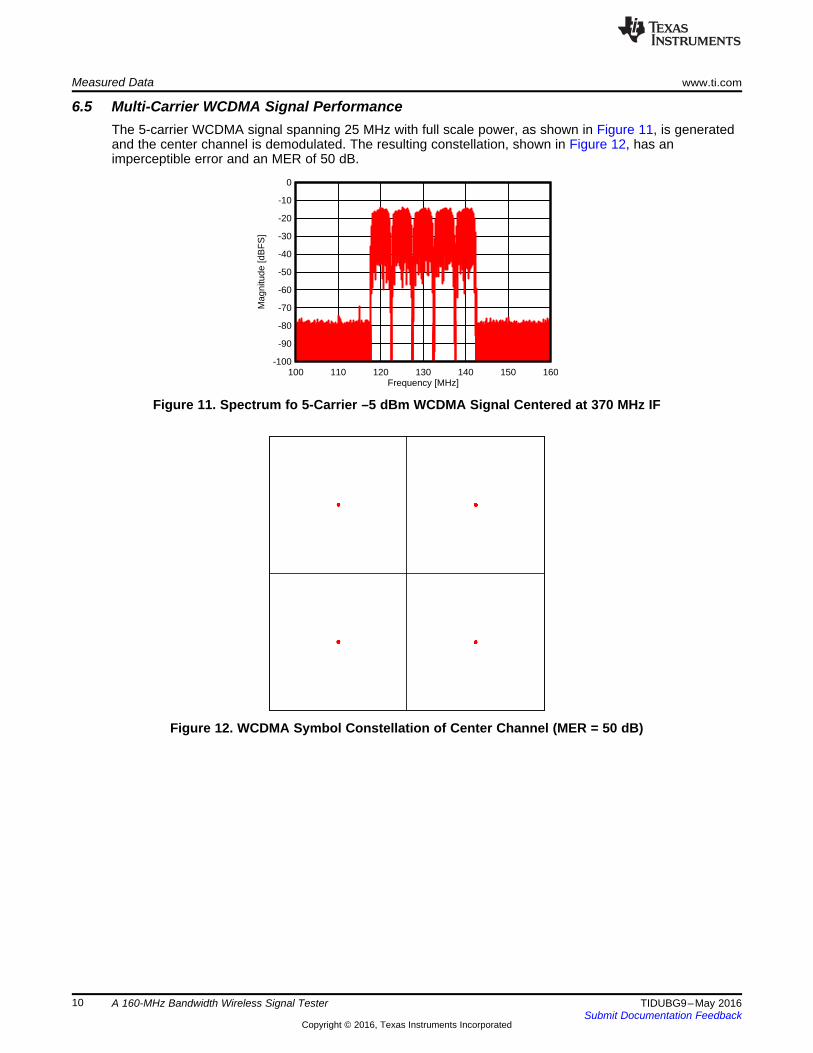
6.5 Multi-Carrier WCDMA Signal PerformanceThe 5-carrier WCDMA signal spanning 25 MHz with full scale power, as shown in Figure 11, is generatedand the center channel is demodulated. The resulting constellation, shown in Figure 12, has animperceptible error and an MER of 50 dB.
Figure 11. Spectrum fo 5-Carrier –5 dBm WCDMA Signal Centered at 370 MHz IF
Figure 12. WCDMA Symbol Constellation of Center Channel (MER = 50 dB)

Frequency [MHz]
Mag
nitu
de [d
BF
S]
0 50 100 150 200 250-100
-90
-80
-70
-60
-50
-40
-30
-20
-10
0
www.ti.com Measured Data
11TIDUBG9–May 2016Submit Documentation Feedback
Copyright © 2016, Texas Instruments Incorporated
A 160-MHz Bandwidth Wireless Signal Tester
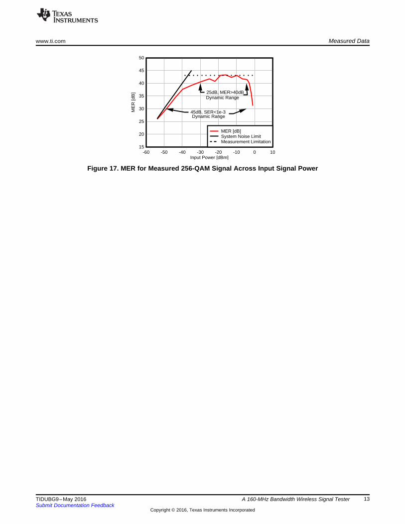
6.6 256-QAM Signal PerformanceMeasurements of the 20 MHz 256-QAM signal (more correctly, a 20-MHz symbol rate signal with alpha=0.22 pulse shaping, which results in 24.4 MHz of bandwidth as shown in Figure 13) show goodcorrespondence with the expected theory. Figure 14, Figure 15, and Figure 16 show a clean constellation,eye diagram, and MER performance for a –5 dBm input signal. Figure 17 shows how the MER dropsbelow 30 dB for a –49 dBm MDS and operates up to 4 dBm input power with a very low signal error rate,above which leads to constellation compressions and errors due to ADC over-range. This gives a signaldetection dynamic range of 45 dB for symbol error rates <10^–3. The usable dynamic range of thissubsystem as a tester is 25 dB for the required MER > 40 dB.
This performance is measured pre-equalizer, which includes amplitude and group delay variation acrossthe 20-MHz bandwidth that degrades the MER. This limitation is usually mitigated by calibration oradaptive equalization in the full tester system. The measurement is also limited by the performance of thesignal generator itself.
Figure 13. Measured Spectrum of 20-MHz 256-QAM Carrier Centered at 370 MHz
Figure 14. Measured 256-QAM Symbol Constellation (MER = 42 dB)

39
39.5
40
40.5
41
41.5
42
42.5
43
Measured Data www.ti.com
12 TIDUBG9–May 2016Submit Documentation Feedback
Copyright © 2016, Texas Instruments Incorporated
A 160-MHz Bandwidth Wireless Signal Tester
Figure 15. Measured 256-QAM Eye Diagram of the In-Phase Signal Path
Figure 16. 256-QAM Measured MER Map for Each Symbol
Input Power [dBm]
ME
R [d
B]
-60 -50 -40 -30 -20 -10 0 1015
20
25
30
35
40
45
50
45dB, SER<1e-3Dynamic Range
25dB, MER>40dBDynamic Range
MER [dB]System Noise LimitMeasurement Limitation
www.ti.com Measured Data
13TIDUBG9–May 2016Submit Documentation Feedback
Copyright © 2016, Texas Instruments Incorporated
A 160-MHz Bandwidth Wireless Signal Tester
Figure 17. MER for Measured 256-QAM Signal Across Input Signal Power
IMPORTANT NOTICE FOR TI REFERENCE DESIGNS
Texas Instruments Incorporated (‘TI”) reference designs are solely intended to assist designers (“Designer(s)”) who are developing systemsthat incorporate TI products. TI has not conducted any testing other than that specifically described in the published documentation for aparticular reference design.TI’s provision of reference designs and any other technical, applications or design advice, quality characterization, reliability data or otherinformation or services does not expand or otherwise alter TI’s applicable published warranties or warranty disclaimers for TI products, andno additional obligations or liabilities arise from TI providing such reference designs or other items.TI reserves the right to make corrections, enhancements, improvements and other changes to its reference designs and other items.Designer understands and agrees that Designer remains responsible for using its independent analysis, evaluation and judgment indesigning Designer’s systems and products, and has full and exclusive responsibility to assure the safety of its products and compliance ofits products (and of all TI products used in or for such Designer’s products) with all applicable regulations, laws and other applicablerequirements. Designer represents that, with respect to its applications, it has all the necessary expertise to create and implementsafeguards that (1) anticipate dangerous consequences of failures, (2) monitor failures and their consequences, and (3) lessen thelikelihood of failures that might cause harm and take appropriate actions. Designer agrees that prior to using or distributing any systemsthat include TI products, Designer will thoroughly test such systems and the functionality of such TI products as used in such systems.Designer may not use any TI products in life-critical medical equipment unless authorized officers of the parties have executed a specialcontract specifically governing such use. Life-critical medical equipment is medical equipment where failure of such equipment would causeserious bodily injury or death (e.g., life support, pacemakers, defibrillators, heart pumps, neurostimulators, and implantables). Suchequipment includes, without limitation, all medical devices identified by the U.S. Food and Drug Administration as Class III devices andequivalent classifications outside the U.S.Designers are authorized to use, copy and modify any individual TI reference design only in connection with the development of endproducts that include the TI product(s) identified in that reference design. HOWEVER, NO OTHER LICENSE, EXPRESS OR IMPLIED, BYESTOPPEL OR OTHERWISE TO ANY OTHER TI INTELLECTUAL PROPERTY RIGHT, AND NO LICENSE TO ANY TECHNOLOGY ORINTELLECTUAL PROPERTY RIGHT OF TI OR ANY THIRD PARTY IS GRANTED HEREIN, including but not limited to any patent right,copyright, mask work right, or other intellectual property right relating to any combination, machine, or process in which TI products orservices are used. Information published by TI regarding third-party products or services does not constitute a license to use such productsor services, or a warranty or endorsement thereof. Use of the reference design or other items described above may require a license from athird party under the patents or other intellectual property of the third party, or a license from TI under the patents or other intellectualproperty of TI.TI REFERENCE DESIGNS AND OTHER ITEMS DESCRIBED ABOVE ARE PROVIDED “AS IS” AND WITH ALL FAULTS. TI DISCLAIMSALL OTHER WARRANTIES OR REPRESENTATIONS, EXPRESS OR IMPLIED, REGARDING THE REFERENCE DESIGNS OR USE OFTHE REFERENCE DESIGNS, INCLUDING BUT NOT LIMITED TO ACCURACY OR COMPLETENESS, TITLE, ANY EPIDEMIC FAILUREWARRANTY AND ANY IMPLIED WARRANTIES OF MERCHANTABILITY, FITNESS FOR A PARTICULAR PURPOSE, AND NON-INFRINGEMENT OF ANY THIRD PARTY INTELLECTUAL PROPERTY RIGHTS.TI SHALL NOT BE LIABLE FOR AND SHALL NOT DEFEND OR INDEMNIFY DESIGNERS AGAINST ANY CLAIM, INCLUDING BUT NOTLIMITED TO ANY INFRINGEMENT CLAIM THAT RELATES TO OR IS BASED ON ANY COMBINATION OF PRODUCTS ASDESCRIBED IN A TI REFERENCE DESIGN OR OTHERWISE. IN NO EVENT SHALL TI BE LIABLE FOR ANY ACTUAL, DIRECT,SPECIAL, COLLATERAL, INDIRECT, PUNITIVE, INCIDENTAL, CONSEQUENTIAL OR EXEMPLARY DAMAGES IN CONNECTION WITHOR ARISING OUT OF THE REFERENCE DESIGNS OR USE OF THE REFERENCE DESIGNS, AND REGARDLESS OF WHETHER TIHAS BEEN ADVISED OF THE POSSIBILITY OF SUCH DAMAGES.TI’s standard terms of sale for semiconductor products (http://www.ti.com/sc/docs/stdterms.htm) apply to the sale of packaged integratedcircuit products. Additional terms may apply to the use or sale of other types of TI products and services.Designer will fully indemnify TI and its representatives against any damages, costs, losses, and/or liabilities arising out of Designer’s non-compliance with the terms and provisions of this Notice.IMPORTANT NOTICE
Mailing Address: Texas Instruments, Post Office Box 655303, Dallas, Texas 75265Copyright © 2016, Texas Instruments Incorporated