a 3-phase ac induction motor control...
TRANSCRIPT
Fre
esc
ale
Se
mic
on
du
cto
r, I
nc
...
Order this documentby AN1857/D
AN1857
A 3-Phase ac Induction Motor Control SystemBased on the MC68HC908MR32By: Bill Lucas and Ken Berringer
Motorola Microcontroller DivisionAustin, Texas
Software Written By:Radim Visinka, Petr Lidak, Pavel Kania, and Petr SteklRoznov System Application LaboratoryRoznov, Czech Republic
Introduction
The use of microcontroller technology has enabled the design of energy-efficient and cost-effective motor control systems. Usingmicrocontrollers (MCU) with specialized pulse-width modulatorinterfaces and integrated protection architecture allows a reasonableapproach to reduce total system cost and increase overall performance.
This application note describes such a system based on the MotorolaMC68HC908MR32 (MR32) motor control specific MCU, optoisolation,and power electronics.
A discussion of the MR32 MCU, hardware design of the control board,optoisolation interface, power electronics, and the required software tocontrol a 3-phase induction motor is presented.
© Motorola, Inc., 2000 AN1857
For More Information On This Product, Go to: www.freescale.com

Application Note
F
ree
sca
le S
em
ico
nd
uc
tor,
I
Freescale Semiconductor, Inc.n
c..
.
A Look at the MC68HC908MR32 Motor Control Microcontroller
The MR32 is a new member of the low-cost, high-performanceM68HC08 (HC08) Family of 8-bit MCUs that are designed specifically formidrange motor control applications.
The Motorola HC08 Family of MCUs is an enhanced, upward objectcode compatible architecture that evolved from the M68HC05 (HC05)Family. All MCUs in the family use the enhanced HC08 centralprocessor unit (CPU08) that includes new addressing modes, many newinstructions, and the performance improvements to existing instructionsthat result from the introduction of instruction pipelining. MCUs in theHC08 Family are available with a variety of package types, input/output(I/O) modules, and various memory sizes and types.
Features of the MR32 motor control MCU include:
• High-performance M68HC08 (CPU08) architecture
• Fully upward-compatible object code with M68HC05, M146805,and M68HC(7)05 Families
• 8-MHz internal bus frequency
• 32 Kbytes of on-chip FLASH memory
• FLASH data security
• 768 bytes of on-chip random-access memory (RAM)
• 12-bit, 6-channel center-aligned or edge-aligned pulse-widthmodulator (PWMMC) module
• Serial peripheral interface module (SPI)
• Serial communications interface module (SCI)
• 16-bit, 4-channel timer interface module (TIMA)
• 16-bit, 2-channel timer interface module (TIMB)
• Clock generator module (CGM)
• Digitally filtered low-voltage inhibit (LVI)
• 10-bit, 10-channel analog-to-digital converter (ADC)
AN1857
2 For More Information On This Product,
Go to: www.freescale.com

Application NoteA Look at the MC68HC908MR32 Motor Control Microcontroller
F
ree
sca
le S
em
ico
nd
uc
tor,
I
Freescale Semiconductor, Inc.n
c..
.
System protection features include:
• Optional computer operating properly (COP) reset
• Low-voltage detection with optional reset
• Illegal opcode detection with optional reset
• Illegal address detection with optional reset
• Fault detection with optional PWM disabling
• Low-power design, fully static with wait mode
• Master reset pin (RST) and power-on reset (POR)
• 64-pin plastic quad flat pack (QFP)
Some CPU08 features include:
• Enhanced M68HC05 programming model
• Extensive loop control functions
• 16 addressing modes (eight more than the HC05)
• 16-bit index register and stack pointer
• Memory-to-memory data transfers
• Fast 8 by 8 bit multiply instruction
• Fast 16/8 bit divide instruction
• Binary-coded decimal (BCD) instructions
• Optimization for controller applications
• Improved C language support
This application note does not discuss in great detail each of the I/Omodules resident on the MR32. Figure 1 shows a block diagram of theMR32. For a detailed description of the MR32, refer to 68HC908MR32,68HC908MR16 Technical Data: Advance Information, Motoroladocument order number MC68HC908MR32/D.
The MR32’s PWMMC module and its protection features make thedevice an excellent choice for use in an embedded motor controlsystem. A review of the PWMMC module and its features is includedhere.
AN1857
3 For More Information On This Product,
Go to: www.freescale.com

Application Note
F
ree
sca
le S
em
ico
nd
uc
tor,
I
Freescale Semiconductor, Inc.n
c..
.
Figure 1. MC68HC908MR32 Block Diagram
MC68HC908MR32 Pulse-Width Modulator
The pulse-width modulator module (PWMMC) resident on the MR32 isspecifically designed to provide pulse-width modulated outputs to drivea power stage connected to a dc servo, brushless dc, or 3-phase acmotor system. The PWMMC module can be partitioned and configuredin several ways, depending on the specific motor control application.Figure 2 shows a block diagram of the PWMMC module and isreferenced throughout this explanation of the PWMMC generator.
Features of the MR32 PWM include:
• Three complementary PWM pairs or six independent PWMsignals
• Complementary mode features include:
– Dead-time insertion
– Separate top/bottom pulse-width correction via currentsensing or programmable software bits
• Edge-aligned PWM or center-aligned PWM signals
• PWM signal polarity
• 20-mA current sink capability on all PWM outputs
• Manual PWM output control through software
• Programmable fault protection
10-CH
ADC
SPI SCI LVI
TIMA4-CH
TIMB2-CH
PWMMC
32K FLASH
768 BYTES RAM
13 I/0 PIN
CPU08
SIM
CGM
PWM1
PWM2
PWM3
PWM4
PWM5
PWM6
FAULTINPUTS
POLARITYSIGNALS
10-BIT
AN1857
4 For More Information On This Product,
Go to: www.freescale.com

Application NoteMC68HC908MR32 Pulse-Width Modulator
F
ree
sca
le S
em
ico
nd
uc
tor,
I
Freescale Semiconductor, Inc.n
c..
.
Figure 2. PWMMC Module Block Diagram
One of the most important features of the PWMMC is its ability to “shutitself down” when a system fault is detected. When dealing with a systemthat potentially could have hundreds of amps of peak current, reacting tofaults such as overcurrent or overvoltage conditions is an absolutenecessity. Fault protection is discussed here first. We then work our wayfrom the outputs of the PWM inward. A discussion of the inputs to thePWM follows.
The six outputs of the PWMMC generator can be configured asindividual pulse-width modulated signals where each output can becontrolled as an independent output. Another option is to configure theoutputs in pairs, with the outputs complementary or not, so drivingcomplementary top and bottom transistors on a power stage becomesan easy task. The outputs of the PWMMC are capable of sinking up to20 mA. That drive capability allows for direct drive of optocouplerswithout the need of additional drivers.
To prevent erroneous signals from being output from the PWMMCmodule while loading new values, the bulk of the registers are doublebuffered and new output is inhibited until a bit in a PWM control register,load okay (LDOK), is set, indicating it is okay to output the new values.
PRESCALER PRESCALERUP/DOWNCOUNTER
PWM RELOADAND INTERRUPT
PWMGENERATORS
CONTROLFAULT
PROTECTION
OUTPUT PWM1
PWM2
PWM3
PWM4
PWM5
PWM6
INTERRUPTS1, 2, 4,O R 8÷ ÷ 1, 2, 4, OR 8
OR
MOTOR CURRENT POLARITIES SYSTEM FAULTS
DOUBLE
BUFFERED
REGISTERS
PWMMODE
SELECT
DEAD-TIME
INSERTION
DIRECTOUTPUT
CONTROL
DISTORTIONCORRECTION
FAULTPARTITIONING
FAULTMODE
SELECT
POLARITYCONTROL
HIGHCURRENTDRIVERS
COMPARATORS
AN1857
5 For More Information On This Product,
Go to: www.freescale.com

Application Note
F
ree
sca
le S
em
ico
nd
uc
tor,
I
Freescale Semiconductor, Inc.n
c..
.
Fault Protection Conditions can arise in the external drive circuitry, requiring that thePWM signals become inactive immediately. These conditions includeovercurrent, overvoltage, overtemperature, or other error conditions.The four fault input pins on the MR32’s PWMMC module can beconfigured to react in a number of different ways, upon the detection ofa fault. Each fault input has its own interrupt vector. In all fault conditions,the output of the PWM generator is forced to a known inactive state.
A number of fault control and recovery options is available to thesystems architect. In some cases, it may be desirable to selectivelydisable PWM(s) solely with software. Manual and automatic recoverymechanisms are available that allow certain acceptable fault situationsto occur, such as starting a motor and using a fault input to limit themaximum startup current. The fault inputs can be partitioned if the MR32is used to control multiple motors.
PWM OutputAlignment
Depending on the system design, there is a choice between edge- orcenter-aligned PWM signals output from the MR32’s PWM generator.The PWM counter uses the value in the timer modulus register todetermine its maximum count.
In center-aligned mode, a 12-bit up/down counter is used to create thePWM period. The PWM resolution in center-aligned mode is two clockperiods (highest resolution is 250 ns @ a processor speed of 8 MHz).The PWM period will be equal to:
[(timer modulus) x (PWM clock period) x 2].
In edge-aligned mode, a 12-bit up-only counter is used to create thePWM period. Therefore, the PWM resolution in edge-aligned mode isone clock (highest resolution is125 ns @ a processor speed of 8 MHz).Again, the timer modulus register is used to determine the maximumcount. The PWM period will be equal to:
[(timer modulus) x (PWM clock period)].
AN1857
6 For More Information On This Product,
Go to: www.freescale.com

Application NoteMC68HC908MR32 Pulse-Width Modulator
F
ree
sca
le S
em
ico
nd
uc
tor,
I
Freescale Semiconductor, Inc.n
c..
.
PWM CounterTimebase
To permit lower PWM frequencies, a prescaler is provided which willdivide the PWM clock frequency by 1, 2, 4, or 8. This prescaler isbuffered and will not be used by the PWM generator until the LDOK bitlocated in a PWM control register is set and a new PWM reload cyclebegins.
PWM LoadOperations
When generating sine waves to a motor, an interrupt routine is typicallyused to step through a sine table located in FLASH memory, scale thatsine value, and output the result to the system from the PWM generator.The rate at which the sine table is scanned can be derived from aninterrupt from the PWM generator. The PWM module can beprogrammed to provide an interrupt rate of every one, two, four, or eightPWM reload cycles.
Direct OutputControl
In some cases, the user may desire to bypass the PWM generator anddirectly control the PWM outputs. A mechanism exists to disconnect thePWM generator from its outputs and directly control the six PWMoutputs. When this mode is used, the PWM generator continues to run;however, its normal PWM output is disabled, overridden by direct output.
Dead-TimeInsertion
When the PWM generator is used in complementary mode, automaticdead-time insertion can be provided to prevent turning on both top andbottom inverter transistors in the same phase leg at the same time.When controlling dc-to-ac inverters, the top and bottom PWMs in onepair must never be active at any given time.
CAUTION: If the top and bottom transistors are turned on simultaneously, largecurrents will flow through the two transistors as they attempt to dischargethe bus supply voltage. The transistors could be weakened or destroyed.
Simply forcing the two PWMs to be inversions of each other is not alwayssufficient. Since a time delay is associated with turning off the transistorsin the motor drive, there must be a “dead-time” between the deactivationof one PWM power transistor and the activation of the opposite transistorin a top and bottom pair.
Dead-time can be specified in the dead-time write-once register. This 8-bit value specifies the number of CPU clock cycles to use for the dead-time.
AN1857
7 For More Information On This Product,
Go to: www.freescale.com

Application Note
F
ree
sca
le S
em
ico
nd
uc
tor,
I
Freescale Semiconductor, Inc.n
c..
.
Motor PhaseCurrent PolaritySensing
Inserting dead-time to protect the top/bottom inverter transistors in amotor drive system is almost always a necessity for ac induction motors.However, inserting this dead-time does not come without a price. Forinstance, when dead-time is inserted, the motor voltage is allowed tofloat momentarily during the dead-time interval, creating distortion in themotor’s current waveform. This distortion can be aggravated bydissimilar turn-on and turn-off delays in the top and bottom transistors.
Three current sensing input pins on the MR32 are labeled IS1–IS3.These inputs are sampled during the dead-time period. The user needsto provide current direction sensing hardware and feed the sensinghardware outputs into the IS1–IS3 inputs. The software then willcompute compensated PWM values and place the two values in anodd/even PWM register pair. From the current direction sensinginformation, the PWM module automatically selects either the odd oreven numbered PWM value register to be used by the PWM generator,thus greatly improving upon the sine wave output quality from the powerstage.
System Hardware
The system consists of several printed circuit boards, power suppliesand a 3-phase induction motor. This section contains a brief descriptionof the individual printed circuit boards (PCB) that comprise the system.
WARNING: The motor control system described in this application note iscapable of operating at dangerous voltages and is capable ofsupplying high amounts of power to rotating machines. Powertransistors, PFC coil, and the motor can reach temperatures hotenough to cause burns. To facilitate safe operation, the high-voltage input power to the power board should come from acurrent-limited dc laboratory power supply. Before moving test oroscilloscope probes, making connections, etc., it is generallyadvisable to power down the high-voltage power supply. Whenhigh voltage is applied, using only one hand for operating the testsetup minimizes the possibility of electrical shock. Operation inlaboratory setups that may have grounded tables and/or chairsshould be avoided. Wearing safety glasses, avoiding ties andjewelry, and using shields also are advisable.
AN1857
8 For More Information On This Product,
Go to: www.freescale.com

Application NoteSystem Hardware
F
ree
sca
le S
em
ico
nd
uc
tor,
I
Freescale Semiconductor, Inc.n
c..
.
MR32 ControlBoard
For a more detailed description of the MR32 control board, refer toMotorola’s Embedded Motion Control Series MR32 Control Board User’sManual (Motorola document order number MEMCMR32CBUM/D) thatcomes with board (kit #ECCTR908MR32).
This document can also be downloaded from the web athttp://mcu.motsps.com/documentation/hc08/devhc08.html. The controlboard is designed as an aid for hardware and software design of single,3-phase, permanent magnet, brush and brushless dc motor driveapplications.
The control board does not contain the MR32 microcontroller. Thecontrol board is designed to be directly connected to an MR32 EM(emulator) board, which is part of an MMDS/MMEVS emulation systemconnected by an impedance matched ribbon cable. A daughter board isdesigned to house the MR32 and will plug into the control board in placeof the emulator cable. With the daughter board plugged into the controlboard, standalone operation of the system is possible.
Because this application note is intended for use with a 3-phase acinduction motor, only the circuitry resident on the MR32 control boardpertaining to the 3-phase ac motor is discussed here. Applications of thecontrol board with other types of motors are covered in additionalapplication notes. Figure 3 shows a complete block diagram of thecontrol board.
Control board features include:
• Six motor control PWM outputs with LED indicators
• Speed control potentiometer
• Optoisolated half duplex RS-232 interface
• Start/Stop and forward/reverse switches
• Hall effect inputs (for brushless dc motor control)
• Back-EMF inputs (for brushless dc motor control)
• Tachometer input configuration jumpers
• 2-position DIP switch for user option control
• Emulator/Daughter board connectors
• Processor reset switch
• Two system fault inputs
• Nine analog inputs
AN1857
9 For More Information On This Product,
Go to: www.freescale.com
Application Note
F
ree
sca
le S
em
ico
nd
uc
tor,
I
Freescale Semiconductor, Inc.n
c..
.
• Three software-controlled LEDs
• On-board regulated power supply
• Motor I/O interface via a ribbon cable connector
Figure 3. MC68HC908MR32 Control Board Block Diagram
For a better understanding of the control board, a description of some ofits circuits follows.
Fault Inputs Two system fault inputs to the control board are designed to protect thepower stage: system bus overvoltage and system bus overcurrent. Theinput signals for these fault comparators originate from signals on thepower board. If an optoisolation board is used in the system, thesesignals are optocoupled and transparently passed to the control boardas an analog signal.
The comparator circuits provide digital signals to the MR32’s fault 1 andfault 2 inputs, respectively. These faults, should one or both occur, willforce the PWM generator into a known inactive state, protecting thepower stage outputs. Figure 4 is a schematic of the circuit used for bothof the fault inputs. The potentiometer, connected to the inverting (–) inputof the comparator, sets its threshold. When the input from the powerboard or optoisolation board exceeds the comparator threshold (voltageat the inverting input to the comparator), the respective fault input to theMR32 is driven to a logic 1, triggering a fault input to the PWM generator.
TERMINAL I/F OPTO-ISOLATEDRS-232
FORWARD/REVERSESWITCH
START/STOPSWITCH
EMULATOR/PROCESSORCONNECTOR
REGULATEDPOWER SUPPLY
dc POWER12–15 Vdc
OPTO/POWER DRIVER I/O CONNECTOR
PWM
CO
NFI
GJU
MPE
RS RESET
SWITCH
OPTIONSWITCHES
SPEEDPOT
TACHINPUT
HALLEFFECTINPUTS
CONNECTOR
BACK-EMFINPUTS
MISC. PWR ANDCONTROL I/O
CURRENT/TEMPSENSE INPUTS
PWMOUTPUTS (6)
OVERCURRENT/OVERVOLTAGE
INPUTS
STATUSLEDS LEDS
40-PIN
AN1857
10 For More Information On This Product,
Go to: www.freescale.com
Application NoteSystem Hardware
F
ree
sca
le S
em
ico
nd
uc
tor,
I
Freescale Semiconductor, Inc.n
c..
.
Adjusting the set-point of the potentiometer allows the user to vary theacceptable system bus current and bus voltage thresholds for faultgeneration. Approximately 20 mV of hysteresis is included in the circuitto aid with noise immunity.
Figure 4. Fault Generation Circuit
Speed Sensing One method used to establish the speed of a motor is to use the analogac output signal from a tachometer generator that is connected to theshaft of the motor. A 16-pole tachometer is coupled to the shaft of themotor as shown in Figure 19. The conditioned signal can then be carriedinto a timer interrupt on the MR32. The period between interrupts is usedto calculate motor shaft speed.
The circuit in Figure 5 is used to “square” the ac signal from thetachometer output into a digital signal acceptable to the timer interruptinput. The input of this circuit has a threshold of approximately 180 mV.Its input hysteresis is set at approximately 20 mV to aid with noiseimmunity.
Figure 5. Tachometer Input Circuit
+
-
+5V_D
OVERVOLTAGE
15 kΩ 15 kΩ 1MΩ
10 kΩ
10 kΩ
GNDA
LM339D
I_DCB_ref/V_DCB_ref
68 pF +5V_A_ref
I_sense/V_sense
Input
7
6
+–
TO TIMER
LM339D
3.3 kΩ10 kΩ
3.3 kΩ 2.2 kΩ15 kΩ
330 kΩ
INTERRUPT
+5V_D+5V_A_ref
+15V_A_ref
560 ΩGND
GNDAGNDA
GNDA 220 nF/100 VMMSZ5230BT1TACHOMETER INPUT
12
5
4
3
12
2
GNDA
AN1857
11 For More Information On This Product,
Go to: www.freescale.com
Application Note
F
ree
sca
le S
em
ico
nd
uc
tor,
I
Freescale Semiconductor, Inc.n
c..
.
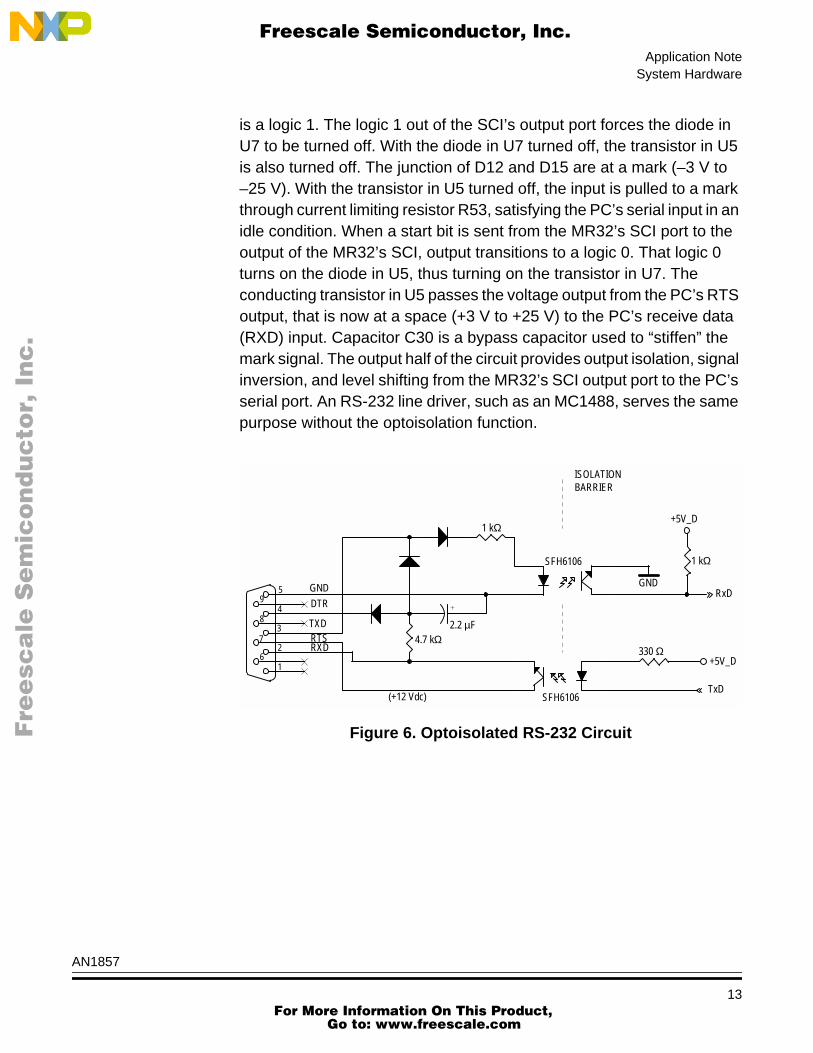
OptoisolatedRS-232 Interface
In the event the control board is used in a system that does not use anoptoisolation board between the control board and the power stage,connection to a computer terminal or PC could be dangerous. The circuitin Figure 6 is the schematic of a half-duplex optoisolated RS-232interface used on the MR32 control board. This isolated terminalinterface provides a margin of safety between the motor control systemand a computer terminal or PC.
The EIA RS-232 specification states the signal levels can range from3volts to 25volts. A mark is defined by the EIA RS-232 specification as
a signal that ranges from –3 volts to –25 volts. A space is defined as asignal that ranges from +3 volts to +25 volts. Therefore, to meet theRS-232 specification, signals to and from a terminal must transitionthrough 0 volts as it changes from a mark to a space. Breaking theisolated RS-232 circuit into input and output sections makes a simplerexplanation of the circuit.
To send data from a PC to the MR32 control board, it is necessary tosatisfy the SCI input on the MR32. In the idle condition, the SCI inputmust be at a logic 1. To accomplish that, the transistor in U6 must be off.The idle state of the transmit data line (TXD) on the PC serial port is amark (–3 V to –25 V). Therefore, the diode in U6 is off and the transistorin U6 is off, yielding a logic 1 to the SCI input. When the start bit is sentto the SCI from the PC’s serial port, the PC’s TXD transitions from amark to a space (+3 V to +25 V), forward biasing the diode in U6.Forward biasing the diode in D3 turns on the transistor in U6, providinga logic 0 to the input of the SCI. Simply stated, the input half of the circuitprovides input isolation, signal inversion, and level shifting from the PCto the MR32’s SCI port. An RS-232 line receiver, such as an MC1489,serves the same purpose without the optoisolation function.
To send data from the MR32 control board to a PC serial port input, it isnecessary to satisfy the PC’s receive data (RXD) input requirements. Inan idle condition, the RXD input to the PC must be at mark (–3 V to–25 V). The data terminal ready output (DTR) on the PC outputs a markwhen the port is initialized. The request to send RTS output is set to aspace (+3 V to +25 V) when the PC’s serial port is initialized. Becausethe interface is half-duplex, the PC’s TXD output is also at a mark, as itis idle. The idle state of the transmit data line (TXD) on the MR32’s SCI
AN1857
12 For More Information On This Product,
Go to: www.freescale.com
Application NoteSystem Hardware
F
ree
sca
le S
em
ico
nd
uc
tor,
I
Freescale Semiconductor, Inc.n
c..
.
is a logic 1. The logic 1 out of the SCI’s output port forces the diode inU7 to be turned off. With the diode in U7 turned off, the transistor in U5is also turned off. The junction of D12 and D15 are at a mark (–3 V to–25 V). With the transistor in U5 turned off, the input is pulled to a markthrough current limiting resistor R53, satisfying the PC’s serial input in anidle condition. When a start bit is sent from the MR32’s SCI port to theoutput of the MR32’s SCI, output transitions to a logic 0. That logic 0turns on the diode in U5, thus turning on the transistor in U7. Theconducting transistor in U5 passes the voltage output from the PC’s RTSoutput, that is now at a space (+3 V to +25 V) to the PC’s receive data(RXD) input. Capacitor C30 is a bypass capacitor used to “stiffen” themark signal. The output half of the circuit provides output isolation, signalinversion, and level shifting from the MR32’s SCI output port to the PC’sserial port. An RS-232 line driver, such as an MC1488, serves the samepurpose without the optoisolation function.
Figure 6. Optoisolated RS-232 Circuit
1 kΩ
4.7 kΩ330 Ω
1 kΩ
GND
DTR
TXDRTSRXD
2.2 µF
ISOLATIONBARRIER
SFH6106
SFH6106
RxD
+5V_D
TxD
+5V_D
(+12 Vdc)
+
1 kΩ
4.7 kΩ330 Ω
1 kΩ
GND
DTR
TXDRTSRXD
2.2 µF
ISOLATIONBARRIER
SFH6106
SFH6106
RxD
+5V_D
TxD
+5V_D
(+12 Vdc)
GND5
94
83
72
61
AN1857
13 For More Information On This Product,
Go to: www.freescale.com

Application Note
F
ree
sca
le S
em
ico
nd
uc
tor,
I
Freescale Semiconductor, Inc.n
c..
.
Back-EMFZero-CrossingDetection
Back-EMF zero-crossing detection enables position recognition whencontrolling brushless dc motors. Sensorless brushless dc motor controlis not discussed in this application note. Rather, refer to SensorlessBrushless dc Motor Using the MC68HC908MR32 Embedded MotionControl Development System, Motorola document order numberAN1858/D, for more information.
To perform distortion correction when controlling a 3-phase ac inductionmotor, it is necessary to provide phase current polarity information to theMR32. That information is detected, signal conditioned on the powerboard, and passed transparently through the optoisolator board to thecontrol board. The three zero-crossing signals from phases A, B and Care routed into the three input current sense IS1–IS3 inputs of the MR32.They are also routed to the back-EMF selection logic, shown inFigure 7. The back-EMF selection logic is designed to provide aninterrupt to the MR32 channel 2 of timer A upon each phase zero-crossing, provided the other input to the NAND gate is at a logic 1. Thethree open collector NAND gates shown in Figure 7 (U7A, U7B, andU7C) are wire ORed such that any one of the these outputs transitioningto a logic 0 will provide an interrupt to the MR32’s timer A.
The system software uses the MUXA, MUXB, and MUXC inputs to theNAND gates to enable a particular phase to have an ability to interruptthe processor. During system operation, the software is aware of thewindow when a particular zero-crossing interrupt should occur for anygiven phase. MUXA, MUXB, and MUXC inputs to the NAND gates areenabled for each particular phase during its computed zero crosswindow. Using this technique, the system is more noise robust,eliminating noise glitches from triggering false interrupts outside of itsparticular “zero cross window.”
AN1857
14 For More Information On This Product,
Go to: www.freescale.com

Application NoteSystem Hardware
F
ree
sca
le S
em
ico
nd
uc
tor,
I
Freescale Semiconductor, Inc.n
c..
.
Figure 7. Zero Cross and Back-EMF Circuit
OptoisolationBoard
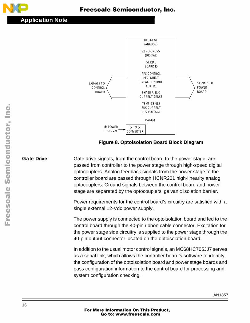
The function of the optoisolation board is to provide a galvanic isolationbarrier between the control board’s I/O, both analog and digital, and thehigh-voltage system power board’s I/O. These isolated signals, to andfrom the optoisolation board, are connected by two 40-pin ribbon cables.Pin assignments for both connectors are the same. Signal flow throughthe optoisolation board, in both directions, is a one-to-one relation of itssource. For a more detailed description of the optoisolation board, referto Motorola’s Embedded Motion Control Series Optoisolation BoardUser’s Manual, Motorola document order number MEMCOBUM/D.Figure 8 shows a block diagram of the optoisolation board.
Zero_cross_A
Zero_cross_B
Zero_cross_C
MUX_A
MUX_B
MUX_C
1/4 MC74HC03AD
+5V_D
BEMF_z_c
5.6 kΩ
1/4 MC74HC03AD
1/4 MC74HC03AD
1/4 MC74HC03AD
+5V_D
5.6 kΩ
AN1857
15 For More Information On This Product,
Go to: www.freescale.com
Application Note
F
ree
sca
le S
em
ico
nd
uc
tor,
I
Freescale Semiconductor, Inc.n
c..
.
Figure 8. Optoisolation Board Block Diagram
Gate Drive Gate drive signals, from the control board to the power stage, arepassed from controller to the power stage through high-speed digitaloptocouplers. Analog feedback signals from the power stage to thecontroller board are passed through HCNR201 high-linearity analogoptocouplers. Ground signals between the control board and powerstage are separated by the optocouplers’ galvanic isolation barrier.
Power requirements for the control board’s circuitry are satisfied with asingle external 12-Vdc power supply.
The power supply is connected to the optoisolation board and fed to thecontrol board through the 40-pin ribbon cable connector. Excitation forthe power stage side circuitry is supplied to the power stage through the40-pin output connector located on the optoisolation board.
In addition to the usual motor control signals, an MC68HC705JJ7 servesas a serial link, which allows the controller board’s software to identifythe configuration of the optoisolation board and power stage boards andpass configuration information to the control board for processing andsystem configuration checking.
BACK-EMF(ANALOG)
ZERO-CROSS(DIGITAL)
SERIALBOARD ID
PFC CONTROLPFC INHIBIT
BREAK CONTROLAUX. I/O
PHASE A, B, CCURRENT SENSE
TEMP. SENSEBUS CURRENTBUS VOLTAGE
PWM(6)
SIGNALS TOCONTROL
BOARD
SIGNALS TOPOWERBOARD
dc TO dcCONVERTER
dc POWER12-15 Vdc
AN1857
16 For More Information On This Product,
Go to: www.freescale.com

Application NoteSystem Hardware
F
ree
sca
le S
em
ico
nd
uc
tor,
I
Freescale Semiconductor, Inc.n
c..
.
OptoisolationBoard
The optoisolation board has a number of individual circuit blocks. Thefirst circuit is a power supply block, supplying +5 Vdc, +3.3 Vdc,+15 Vdc, and –15 Vdc to the board. The power circuits are comprised ofindividual linear regulators. The next circuit is a digital optoisolationcircuit. The last circuit is a linear optoisolation circuit. A discussion of theoptoisolation blocks follows.
DigitalOptoisolationCircuit
Figure 9 is a simplified schematic diagram of the basic design of thedigital optoisolation circuit used on the optoisolation board. The circuitsare used to couple several control signals from the control board to thepower board. Those signals are the six PWM signals, one sparebidirectional optoisolation I/O, one PFC inhibit, one PFC PWM, and onemotor brake control signal from the controller board to the power stage.Also, the optoisolation board is used to couple four digital feedbacksignals from the power board to the control board. Those signals arephases A, B, and C zero cross signals and a PFC zero cross signal.
Figure 9. Digital Optoisolation Circuit
The digital isolation block is based on Agilent Technologies’ HCPL-J454high dv/dt coupler. A simplified schematic is shown in Figure 9. Whenthe MR32 is reset, and until its I/O has been set up by the systemsoftware, in most cases, its outputs are three-stated. R1 sets a logic lowin the absence of a signal. Open input pull down is important for gatedrive signals, where it is desirable to keep power transistors off in caseof either a broken connection or absence of power on the control boardor until the I/O ports have been set up.
DIGITAL SIGNAL IN
R110 kΩ
GND_CBGND_CB
1
2
14
7
3
330 Ω
3
D1
2
+5V_D_CB+5V_D_PS
+5V_D_CB
ANODE
CATHODE
ISO1
Q1HCPL-J454#300
GND_PS
GND5
6
8 R3
1.8 kΩD2
VCC
VOut 3 4
U1AMC74HCT00AD
U2AMC74HCT14AD
DIGITAL SIGNAL OUTR2
AN1857
17 For More Information On This Product,
Go to: www.freescale.com

Application Note
F
ree
sca
le S
em
ico
nd
uc
tor,
I
Freescale Semiconductor, Inc.n
c..
.
Next, NAND gate, U1A, inverts the input signal. Assuming a logic low atthe input (across R1), U1A’s output is high. With no forward bias on theinput diode of the optocoupler, the optocoupler’s output transistor is off,producing a logic high. This logic high is inverted by U2A to produce alogic low at the output. Conversely, when the input (across R1) is high,the output of U1A is low. Forward bias at the input of the optocouplercauses light to shine on the optocoupler’s photodiode which produces aleakage current that flows into the optocoupler’s base. With base currentsupplied, the optocoupler’s transistor is on and the optocoupler’s outputis low. That low input into U2A causes the output of U2A is go high. Theblock as a whole, therefore, is non-inverting.
AnalogOptoisolationCircuit
Figure 10 is a simplified schematic diagram of the basic design of theanalog optoisolation circuit used on the optoisolation board. The circuitsare used to couple several feedback signals from the power board to thecontroller board. Those signals are the phases A, B, and C currentfeedback, system bus current, and bus voltage, heatsink temperatureand phase A, B, and C back-EMF signals.
Figure 10. Analog Optoisolation Circuit
ANALOG INPUT
GNDA_PS GNDA_CB
R3
100 kΩ
56 7R1
100 kΩ
R2
100 Ω(VIn)
A1
MC34072D LEDISO1
1
23
4
6
5
56
7A2
ANALOG OUTPUT(VOut)
4MC33502/D
HCNR201#300
PD1 PD2+–
+–
AN1857
18 For More Information On This Product,
Go to: www.freescale.com

Application NoteSystem Hardware
F
ree
sca
le S
em
ico
nd
uc
tor,
I
Freescale Semiconductor, Inc.n
c..
.
The analog isolation block is based on Agilent Technologies’ HCNR201high-linearity optocoupler. The HCNR201 consists of an LED and twophotodiodes. The LED and one of the photodiodes (PD1) is on the inputside of the optoisolation barrier, and the other photodiode (PD2) is on theoutput side. The package is constructed so that each photodiodereceives approximately the same amount of light from the LED.Feedback amplifier, A1, is configured with PD1 to monitor the lightoutput of the LED and automatically adjust LED current to compensatefor any non-linearity. The output photodiode then converts a stable,linear light output of the LED into a current, which is then converted backinto a voltage by amplifier A2.
Circuit operation may not be immediately obvious from inspectingFigure 10, particularly the input part of the circuit. Stated briefly,amplifier A1 adjusts LED forward current (IF) such that the current in PD1(IPD1) is equal to VIn/R1.
Analysis of the input circuit reveals that increasing the input voltageincreases the voltage at the inverting input terminal of A1. Amplifier A1amplifies that increase, causing IF and IPD1 to increase. Given the waythat PD1 is connected, IPD1 will pull the inverting input of the op-ampback toward ground. A1 will continue to increase IF until its invertinginput voltage stabilizes near its ground reference voltage. Assuming thatno current flows into the inputs of A1, all of the current flowing throughR1 will flow through PD1. Since the inverting input of A1 is atapproximately 0 volts, the current through R1, and therefore IPD1, isequal to VIn /R1. Essentially, amplifier A1 adjusts IF such thatIPD1 = –VIn/R1. Note that IPD1 depends only on the input voltage and thevalue of R1 and is independent of the optocoupler’s characteristics. Alsonote that IPD1 is directly proportional to VIn, giving a very linearrelationship between the input voltage and the photodiode current.
The physical construction of the optocoupler’s package determines therelative amounts of light that fall on the two photodiodes and, therefore,the ratio of the photodiode currents. This results in a current, IPD2, thatis very nearly equal to IPD1. Amplifier A2 and resistor R3 form a trans-resistance amplifier that converts IPD2 back into a voltage, VOut, whereVOut = IPD2 * R3. Combining input and output equations results in anexpression that relates the output voltage to the input voltage,VOut/VIn = (R3/R1). Therefore, with R1 = R3, the output signal closelymatches the input.
AN1857
19 For More Information On This Product,
Go to: www.freescale.com

Application Note
F
ree
sca
le S
em
ico
nd
uc
tor,
I
Freescale Semiconductor, Inc.n
c..
.
Power Stage
For a more detailed description of the 3-phase ac BLDC high-voltagepower stage, refer to the Motorola Embedded Motion Control Series3-Phase BLDC High-Voltage Power Stage User’s Manual, Motoroladocument order number MEMC3PBLDCPSUM/D.
The function of the power stage is to provide the high-power drivecircuitry for various types of motors. The power stage is suitable fordriving ac induction, permanent magnet, and brush and brushless dcmotors.
The power stage consists of a set of two printed circuit boards (PCB).One of the PCBs is a power module, containing power IGBTs (insulatedgate bipolar transistors), a brake IGBT, a power factor corrector FET(field-effect transistor), and temperature-sensing diodes. The secondPCB contains IGBT drive circuits, analog signal conditioning, low-voltage power supplies, power factor control circuitry, and anMC68HC705JJ7 microcontroller used for board configuration andidentification. Figure 11 shows a complete block diagram of the powermodule.
Power module features include:
• 1-phase bridge rectifier
• Power factor switch and diode
• dc-bus brake IGBT and brake current limiting resistors
• 3-phase bridge inverter (six IGBTs)
• Individual phase and dc bus current sensing shunt resistors withKelvin connections
• Power stage temperature sensing diodes
• IGBT gate drivers
• Current and temperature signal conditioning
• 3-phase back-EMF voltage sensing and zero cross detectioncircuitry
• Board identification processor (MC68HC705JJ7)
• Low-voltage on-board power supplies
• Cooling fans
AN1857
20 For More Information On This Product,
Go to: www.freescale.com

Application NotePower Stage
F
ree
sca
le S
em
ico
nd
uc
tor,
I
Freescale Semiconductor, Inc.n
c..
.
Figure 11. Power Module Block Diagram
For a better understanding of the power stage, a description of severalof its circuits follows.
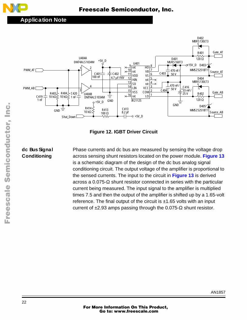
Power SwitchDriver Circuitry
Figure 12 is a schematic diagram of the basic design of the power switchdriver circuitry. The IGBT drivers, IR2112S, provide control of the powerIGBT power switches by shifting and transforming the PWM logic levelcontrol signals to the levels necessary to control the power switches.
The turn-on time of the IGBT power switch is controlled by resistorsR401 and R402 which are connected to the power switch gates. DiodesD402 and D404 aid in a fast turn off of the IGBT power switches byproviding a low-impedance path back to the IR2112S to discharge thepower switch’s gate. D401 protects the power supply and any othercircuits connected to it by preventing high voltage that could flow out ofthe VB power input (pin 7) to the IR2112S.
If an overcurrent situation should occur, the overcurrent circuit on thepower module will supply a shut down signal to the IR2112S, turning offits outputs, thus protecting the power switches. At the input, pull downresistors, R403 and R404, set a logic low in the absence of a signal.Open input pull down is important for gate drive signals, where it isdesirable to keep power transistors off in case of either a brokenconnection or absence of power on the control board.
HV POWERINPUT SWITCH MODE
POWER SUPPLYPFC CONTROLdc BUS BRAKE
IGBT POWER
GATE
PHASE CURRENTPHASE VOLTAGE
BUS CURRENTBUS VOLTAGE
MONITOR
ZERO CROSSBACK-EMF SENSE
BOARDID BLOCK
3-PHASE ACSIGNALSTO/FROMCONTROL
BOARD
MODULE
DRIVERS MOTORTO
AN1857
21 For More Information On This Product,
Go to: www.freescale.com
Application Note
F
ree
sca
le S
em
ico
nd
uc
tor,
I
Freescale Semiconductor, Inc.n
c..
.
Figure 12. IGBT Driver Circuit
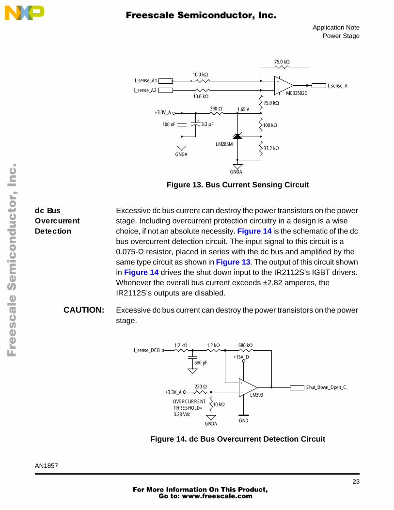
dc Bus SignalConditioning
Phase currents and dc bus are measured by sensing the voltage dropacross sensing shunt resistors located on the power module. Figure 13is a schematic diagram of the design of the dc bus analog signalconditioning circuit. The output voltage of the amplifier is proportional tothe sensed currents. The input to the circuit in Figure 13 is derivedacross a 0.075-Ω shunt resistor connected in series with the particularcurrent being measured. The input signal to the amplifier is multipliedtimes 7.5 and then the output of the amplifier is shifted up by a 1.65-voltreference. The final output of the circuit is ±1.65 volts with an inputcurrent of ±2.93 amps passing through the 0.075-Ω shunt resistor.
910111213141516
87654321
PWM_AT
PWM_AB
C4191 nF
R40310 kΩ
R40410 kΩ
C4201 nF
U404BDM74ALS1034M
U404ADM74ALS1034M
1 2
34
GND
Shut_Down
R41410 kΩ
+5V_D
R413100 Ω
+5V_D
C4138.2 pf
GND
+5V_D
C401100 nF
C4024.7 µF/16V
U401n/cn/cVDDHINSDLINVSSn/c
HOVBVSn/cn/c
VCCCOM
LOIR2112S
C404
470 nF/50 V
470 nF/50 VC403
D401MURS160T3
C41633 mF/25 V
+
+15V_D
D402MBRS130LT3
D404MBRS130LT3
D403
MMSZ5251BT1
D405MMSZ5251BT1
R401
120 Ω
R402
120 ΩGND
Gate_AT
Source_AT
Gate_AB
Source_AB
AN1857
22 For More Information On This Product,
Go to: www.freescale.com
Application NotePower Stage
F
ree
sca
le S
em
ico
nd
uc
tor,
I
Freescale Semiconductor, Inc.n
c..
.
Figure 13. Bus Current Sensing Circuit
dc BusOvercurrentDetection
Excessive dc bus current can destroy the power transistors on the powerstage. Including overcurrent protection circuitry in a design is a wisechoice, if not an absolute necessity. Figure 14 is the schematic of the dcbus overcurrent detection circuit. The input signal to this circuit is a0.075-Ω resistor, placed in series with the dc bus and amplified by thesame type circuit as shown in Figure 13. The output of this circuit shownin Figure 14 drives the shut down input to the IR2112S’s IGBT drivers.Whenever the overall bus current exceeds ±2.82 amperes, theIR2112S’s outputs are disabled.
CAUTION: Excessive dc bus current can destroy the power transistors on the powerstage.
Figure 14. dc Bus Overcurrent Detection Circuit
+
+
-I_sense_A1
I_sense_A2
10.0 kΩ
10.0 kΩ
75.0 kΩ
100 kΩ
33.2 kΩ
390 Ω
100 nF 3.3 µF
LM285M
GNDA
GNDA
+3.3V_A
75.0 kΩ
MC33502DI_sense_A
1.65 V
+
-
I_sense_DCB1.2 kΩ
680 pF
+3.3V_A220 Ω
10 kΩ
680 kΩ
LM393
Shut_Down_Open_C.
+15V_D
GNDAGND
1.2 kΩ
OVERCURRENTTHRESHOLD=3.23 Vdc
AN1857
23 For More Information On This Product,
Go to: www.freescale.com
Application Note
F
ree
sca
le S
em
ico
nd
uc
tor,
I
Freescale Semiconductor, Inc.n
c..
.
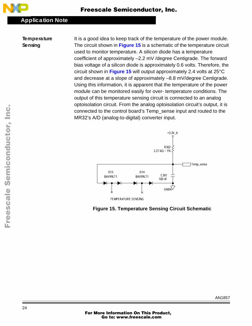
TemperatureSensing
It is a good idea to keep track of the temperature of the power module.The circuit shown in Figure 15 is a schematic of the temperature circuitused to monitor temperature. A silicon diode has a temperaturecoefficient of approximately –2.2 mV /degree Centigrade. The forwardbias voltage of a silicon diode is approximately 0.6 volts. Therefore, thecircuit shown in Figure 15 will output approximately 2.4 volts at 25°Cand decrease at a slope of approximately –8.8 mV/degree Centigrade.Using this information, it is apparent that the temperature of the powermodule can be monitored easily for over- temperature conditions. Theoutput of this temperature sensing circuit is connected to an analogoptoisolation circuit. From the analog optoisolation circuit’s output, it isconnected to the control board’s Temp_sense input and routed to theMR32’s A/D (analog-to-digital) converter input.
Figure 15. Temperature Sensing Circuit Schematic
GNDA
R3022.21 kΩ – 1%
C301100 nF
+3.3V_A
Temp_sense
D14BAV99LT1
D13BAV99LT1
TEMPERATURE SENSING
AN1857
24 For More Information On This Product,
Go to: www.freescale.com

Application NotePower Stage
F
ree
sca
le S
em
ico
nd
uc
tor,
I
Freescale Semiconductor, Inc.n
c..
.
dc Bus Brake Under certain operating conditions, a motor can act as a generator,delivering high voltage back into the dc bus through the inverter’s powerswitches and/or the power switch source-drain recovery diodes. That isa very undesirable condition and can damage the power transistors andother components in the inverter. The excess energy must bedissipated; otherwise, the dc bus voltage will rise above a safe limit. Thepower module contains an IGBT and current limiting resistors, placedacross the dc bus to act as a dc bus brake and dissipate the excessenergy. Figure 16 is a schematic of the dc bus brake control circuitry.When using the brake, care must be taken to not exceed the powerdissipation of the brake transistor and its current limit resistors.Provisions are made on the power board for the user to install anadditional brake resistor across the one composed of R6–R9, allowingfor additional bus brake current to be imposed on the system. Again,care must be taken not to exceed the ratings of the IGBT brake transistorwhen an additional brake resistor is installed in the system. Typically, thesystem software will pulse-width modulate the brake to dissipate theexcess voltage until it is brought down to an acceptable level.
CAUTION: Under certain operating conditions, a motor can act as a generator,delivering high voltage back into the dc bus through the inverter’s powerswitches and/or the power switch source-drain recovery diodes. Thiscan damage the power transistors and other components in the inverter.
Figure 16. dc Bus Brake Circuit Schematic
Brake_control
R20210 kΩ
GND
C2121 nF
1
2
4
8
7
5
GND GND
U202
NCInA
InB
NC
OutA
OutB
3
C202
10 µF/35 V
C203
100 nF GND
MC33152D
VCC6
R204
100 Ω D201MMSZ5251BT1 DC Bus –
+15V_D
R6250 Ω
R7250 Ω
DC Bus +
Brake_Res
Q7SGB04N60
R8250 Ω
R9250 Ω
D11HFA04TB60S
DCB_Cap_Pos
DCB_Cap_Neg
+
AN1857
25 For More Information On This Product,
Go to: www.freescale.com
Application Note
F
ree
sca
le S
em
ico
nd
uc
tor,
I
Freescale Semiconductor, Inc.n
c..
.
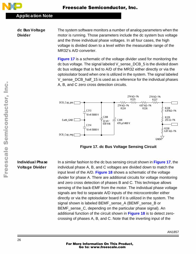
dc Bus VoltageDivider
The system software monitors a number of analog parameters when themotor is running. Those parameters include the dc system bus voltageand the three individual phase voltages. In all four cases, the highvoltage is divided down to a level within the measurable range of theMR32’s A/D converter.
Figure 17 is a schematic of the voltage divider used for monitoring thedc bus voltage. The signal labeled V_sense_DCB_5 is the divided downdc bus voltage that is fed to A/D of the MR32 either directly or via theoptoisolator board when one is utilized in the system. The signal labeledV_sense_DCB_half_15 is used as a reference for the individual phasesA, B, and C zero cross detection circuits.
Figure 17. dc Bus Voltage Sensing Circuit
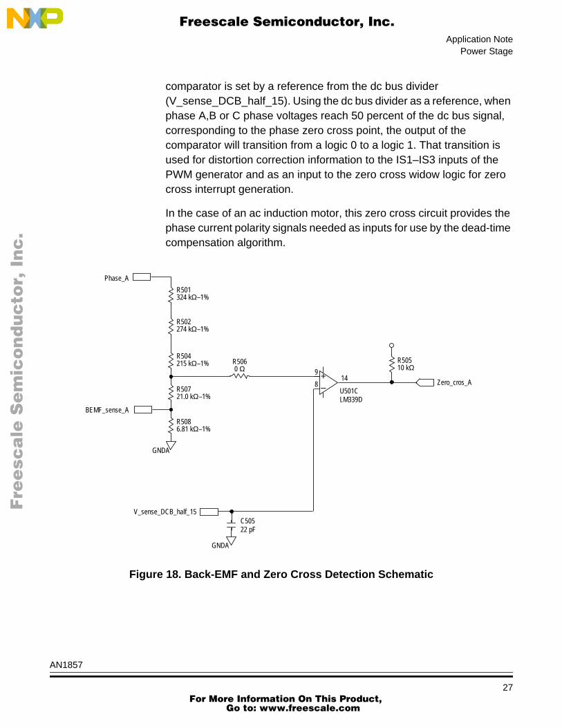
Individual PhaseVoltage Divider
In a similar fashion to the dc bus sensing circuit shown in Figure 17, theindividual phase A, B, and C voltages are divided down to match theinput level of the A/D. Figure 18 shows a schematic of the voltagedivider for phase A. There are additional circuits for voltage monitoringand zero cross detection of phases B and C. This technique allowssensing of the back-EMF from the motor. The individual phase voltagesignals are fed to separate A/D inputs of the microcontroller eitherdirectly or via the optoisolator board if it is utilized in the system. Thesignal shown is labeled BEMF_sense_A (BEMF_sense_B orBEMF_sense_C, depending on the particular phase signal). Anadditional function of the circuit shown in Figure 18 is to detect zero-crossing of phases A, B, and C. Note that the inverting input of the
GNDA
DCB_Cap_pos
Earth_GND
DCB_Cap_neg
C213
10 nF/3000 V
C214
10 nF/3000 V
C208
22 nF/630 Vdc
C209470 µF/400 V
+
274 kΩ–1%R224
274 kΩ–1%R225
4.87 kΩ–1%R226
274 kΩ–1%R227
R229255 Ω–1%
R2286.81kΩ–1%
R2306.81 kΩ–1%
AN1857
26 For More Information On This Product,
Go to: www.freescale.com
Application NotePower Stage
F
ree
sca
le S
em
ico
nd
uc
tor,
I
Freescale Semiconductor, Inc.n
c..
.
comparator is set by a reference from the dc bus divider(V_sense_DCB_half_15). Using the dc bus divider as a reference, whenphase A,B or C phase voltages reach 50 percent of the dc bus signal,corresponding to the phase zero cross point, the output of thecomparator will transition from a logic 0 to a logic 1. That transition isused for distortion correction information to the IS1–IS3 inputs of thePWM generator and as an input to the zero cross widow logic for zerocross interrupt generation.
In the case of an ac induction motor, this zero cross circuit provides thephase current polarity signals needed as inputs for use by the dead-timecompensation algorithm.
Figure 18. Back-EMF and Zero Cross Detection Schematic
+–
GNDA
GNDA
R501324 kΩ–1%
R502274 kΩ–1%
R504215 kΩ–1%
R50721.0 kΩ–1%
R5086.81 kΩ–1%
R5060 Ω
C50522 pF
Phase_A
BEMF_sense_A
9
814
U501CLM339D
R50510 kΩ
Zero_cros_A
V_sense_DCB_half_15
AN1857
27 For More Information On This Product,
Go to: www.freescale.com

Application Note
F
ree
sca
le S
em
ico
nd
uc
tor,
I
Freescale Semiconductor, Inc.n
c..
.
Power FactorCorrection
Power factor correction control (PFC) circuitry provides control of thePFC switch and handles the necessary feedback to provide a sinusoidalpower line current. The capability of PFC can be enabled or disabled bychanging a jumper configuration on the power module. The jumper canbe found in proximity to the dc bus capacitor. The objective of the PFChardware and software is to draw sinusoidal current from the ac mainsupply power in an attempt to approach as close as possible a unitypower factor. The circuitry on the power board is a boost power supply,controlled by the MR32 on the control board. Without PFC, the currentfrom the ac main supply tends to draw current at the peak of the ac sinewave.
Describing the control of the PFC circuity exceeds the scope of thisapplication note. A forthcoming application note will describe PFCcontrol in detail.
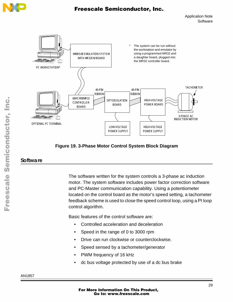
3-Phase MotorControl SystemConfiguration
Figure 19 is a block diagram of the complete 3-phase motor controlsystem configuration with an MMDS05/08 emulation system and PCworkstation. An optional PC, connected to the MR32 control board, isshown. The optional PC can be used to communicate control systemparameters to the system via software running on the control board. Thesystem may be exercised in standalone mode, without the MMDS05/08emulator and PC workstation, by placing a programmed MR32 into thedaughter board and plugging it into the control board in place of theMMDS05/08 emulator system.
AN1857
28 For More Information On This Product,
Go to: www.freescale.com
Application NoteSoftware
F
ree
sca
le S
em
ico
nd
uc
tor,
I
Freescale Semiconductor, Inc.n
c..
.
Figure 19. 3-Phase Motor Control System Block Diagram
Software
The software written for the system controls a 3-phase ac inductionmotor. The system software includes power factor correction softwareand PC-Master communication capability. Using a potentiometerlocated on the control board as the motor’s speed setting, a tachometerfeedback scheme is used to close the speed control loop, using a PI loopcontrol algorithm.
Basic features of the control software are:
• Controlled acceleration and deceleration
• Speed in the range of 0 to 3000 rpm
• Drive can run clockwise or counterclockwise.
• Speed sensed by a tachometer/generator
• PWM frequency of 16 kHz
• dc bus voltage protected by use of a dc bus brake
PC WORKSTATION*
OPTIONAL PC TERMINAL
MMDS08 EMULATION SYSTEMWITH MR32EM BOARD
68HC908MR32CONTROLLER
BOARD
40-PINRIBBON
40-PINRIBBON
OPTOISOLATIONBOARD
LOW-VOLTAGEPOWER SUPPLY
HIGH-VOLTAGEPOWER BOARD
HIGH-VOLTAGEPOWER SUPPLY
TACHOMETER
3-PHASE ACINDUCTION MOTOR
* The system can be run withoutthe workstation and emulator byusing a programmed MR32 anda daughter board, plugged intothe MR32 controller board.
AN1857
29 For More Information On This Product,
Go to: www.freescale.com

Application Note
F
ree
sca
le S
em
ico
nd
uc
tor,
I
Freescale Semiconductor, Inc.n
c..
.
Features of the PC-Master communication software include:
• Ability to read/write any RAM (random-access memory) variable
• Read any ROM (read-only memory) variable
• Execute PC-Master commands
Features of the power factor correction software include:
• Automatic calibration of the control PFC loop
• Automatic input voltage detection 110 V/60 Hz and 230 V/50 Hz
Software Design This section describes the design and functionality of the systemsoftware that executes in the MMDS05/08 emulator system or in aprogrammed MR32, resident on a daughter board, plugged into thecontrol board.
PC-Master PC-Master communication software is intended to be used as an aid indeveloping motor control software. All of the required actions of themotor control software are manipulated by the operator when using thePC-Master software. The PC-Master software executes on a PC that isconnected to the isolated RS-232 serial port on the control board. ThePC-Master software executing on a PC uses Microsoft Internet Exploreras a user interface to the PC.
A small program is resident in the MR32 that communicates with the PC-Master software to parse commands, return status information to thePC, and process control information from the PC.
The actions controlled by the PC-Master are:
• Start/Stop control
• Motor speed setpoint
• Reset the drive system
• Motor rotation direction control (CW/CCW)
AN1857
30 For More Information On This Product,
Go to: www.freescale.com

Application NoteSoftware
F
ree
sca
le S
em
ico
nd
uc
tor,
I
Freescale Semiconductor, Inc.n
c..
.
Variables read by the PC-Master software as a default and displayed tothe user are:
• Required speed
• Actual motor speed
• dc bus voltage
• Power module temperature
• Display system status and error flags
For the latest information regarding the PC-Master software, refer to theMotorola, Semiconductor Products Sector, Motor Control web page:http://motorola.com/semiconductors/motor.
For the latest application note software, refer to the following web links:http://www.mcu.motsps.com/dev_tools/appsw.htmlhttp://motorola.com/semiconductors/motorhttp://motorola.com/semiconductors
System Software The motor drive can be controlled in two ways.
• In the manual operation mode, speed is set by the potentiometer,start/stop and forward/reverse controls are mounted on the controlboard.
• In the PC-Master mode of operation, all motor drive control isperformed from commands from a PC connected to the controlboard.
The motor control software monitors the state of the sensors as they areperiodically scanned in the software timer loop, while the speed of themotor is calculated utilizing the input capture interrupt. Whenever themotor is running, a green LED located on the control board willilluminate. According to the operational mode setup and state of thecontrol signals (start/stop switch, forward/reverse switch, speedpotentiometer), the speed command is calculated using anacceleration/deceleration ramp. The comparison between the actualspeed command and the tachometer speed generates a speed error.The speed error is passed to the speed PI controller generating a newcorrected motor frequency. Using a V/Hz ramp, the corresponding
AN1857
31 For More Information On This Product,
Go to: www.freescale.com

Application Note
F
ree
sca
le S
em
ico
nd
uc
tor,
I
Freescale Semiconductor, Inc.n
c..
.
voltage is calculated. The PWM generation process calculates a systemof 3-phase voltages of the required amplitude and frequency thatincludes dead-time. The 3-phase PWM motor control signals are thenoutput to the power stage.
The dc bus voltage and dc bus current are measured during the controlprocess. They are used for overvoltage and overcurrent protection of thedrive. The overvoltage protection is performed by software while theovercurrent fault signal utilizes a fault input of the microcontroller.
If any of the aforementioned faults occur, the motor control PWM outputsare disabled to protect the drive. The system fault state also is displayed.These faults, depending on the operating mode of the system, are outputto the LEDs on the controller and/or the PC terminal connected to thecontrol board.
The design of the system requires the system software to take somevalues from the user interface and sensors, processes them, andgenerates 3-phase PWM signals for motor control.
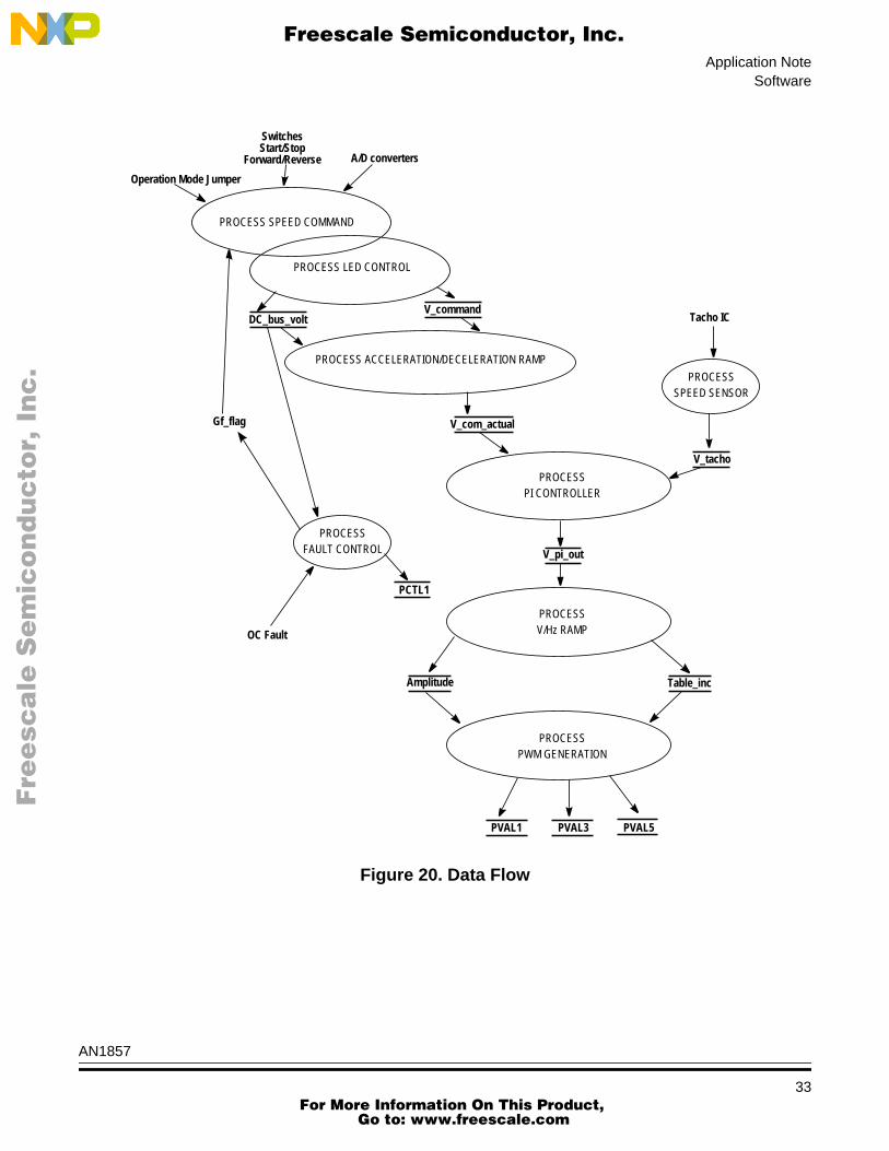
The control algorithm for a close loop ac drive is described in Figure 20.It consists of processes described in following subsections. Specialattention is given to the subroutine’s 3-phase PWM calculation and voltsper hertz control algorithm. Also, initialization of the microcontroller isdescribed.
AN1857
32 For More Information On This Product,
Go to: www.freescale.com
Application NoteSoftware
F
ree
sca
le S
em
ico
nd
uc
tor,
I
Freescale Semiconductor, Inc.n
c..
.
Figure 20. Data Flow
PROCESS SPEED COMMAND
DC_bus_volt
PROCESS LED CONTROL
PROCESS ACCELERATION/DECELERATION RAMP
PROCESSSPEED SENSOR
PROCESSFAULT CONTROL
PROCESSPI CONTROLLER
PROCESSV/Hz RAMP
PROCESSPWM GENERATION
V_command
V_com_actual
PCTL1
V_pi_out
V_tacho
Amplitude Table_inc
PVAL3 PVAL5PVAL1
Operation Mode Jumper
Switches
Forward/ReverseStart/Stop
A/D converters
Tacho IC
Gf_flag
OC Fault
AN1857
33 For More Information On This Product,
Go to: www.freescale.com

Application Note
F
ree
sca
le S
em
ico
nd
uc
tor,
I
Freescale Semiconductor, Inc.n
c..
.
When the MR32 is reset, the software configures the various system I/O.The forward/reverse switch, start/stop switch, and dc bus voltage arechecked, and the speed potentiometer’s value is input. A yellow LEDlocated on the control board is illuminated when the system is ready. Theidentification of the connected boards (optoisolator and power boards) ischecked. The default operation mode is set to manual. The PC-Masteroperation mode can be set by the PC-Master command. The PFCalgorithm is initialized. After the initialization is passed, the fault flag(failure) is tested for any system faults. Anytime a fault is detected in thesystem, a red LED located on the control board will illuminate. Thesystem name for dc bus voltage is Out_volt_new. The value input fromthe speed pot is labeled Pot_voltage.
The input parameters of the process are evaluated and the speedcommand V_command is calculated accordingly. Also, the dc busvoltage, named dc_bus_volt, is measured. The general fault Gf_flag isanalyzed and the state of the drive is set. The drive state diagram isshown in Figure 21. The status LEDs are controlled according thesystem state.
The calculated speed command V_command is a 2-byte variable withthe format (1 Hz = 0x0100). The upper byte represents the integerportion and the lower byte represents the fractional portion of the value.This format is kept through all the program for all the speed variables.
The system software calculates a new speed based on the requestedspeed, according to the acceleration/deceleration ramp.
AN1857
34 For More Information On This Product,
Go to: www.freescale.com
Application NoteSoftware
F
ree
sca
le S
em
ico
nd
uc
tor,
I
Freescale Semiconductor, Inc.n
c..
.
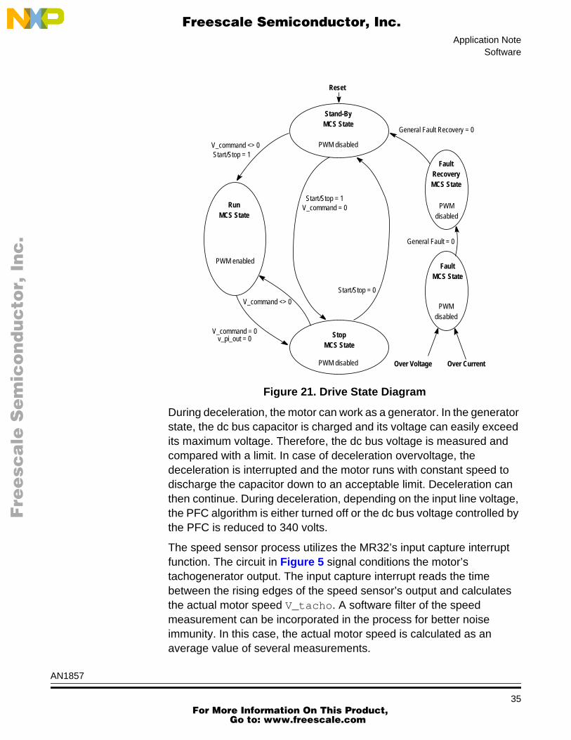
Figure 21. Drive State Diagram
During deceleration, the motor can work as a generator. In the generatorstate, the dc bus capacitor is charged and its voltage can easily exceedits maximum voltage. Therefore, the dc bus voltage is measured andcompared with a limit. In case of deceleration overvoltage, thedeceleration is interrupted and the motor runs with constant speed todischarge the capacitor down to an acceptable limit. Deceleration canthen continue. During deceleration, depending on the input line voltage,the PFC algorithm is either turned off or the dc bus voltage controlled bythe PFC is reduced to 340 volts.
The speed sensor process utilizes the MR32’s input capture interruptfunction. The circuit in Figure 5 signal conditions the motor’stachogenerator output. The input capture interrupt reads the timebetween the rising edges of the speed sensor’s output and calculatesthe actual motor speed V_tacho. A software filter of the speedmeasurement can be incorporated in the process for better noiseimmunity. In this case, the actual motor speed is calculated as anaverage value of several measurements.
Reset
Stand-ByMCS State
PWM disabled
Start/Stop = 1V_command = 0
Start/Stop = 1V_command <> 0
RunMCS State
PWM enabled
V_command <> 0
V_command = 0v_pi_out = 0
Start/Stop = 0
StopMCS State
PWM disabled
FaultMCS State
PWMdisabled
Over Voltage Over Current
General Fault = 0
FaultRecoveryMCS State
PWMdisabled
General Fault Recovery = 0
AN1857
35 For More Information On This Product,
Go to: www.freescale.com

Application Note
F
ree
sca
le S
em
ico
nd
uc
tor,
I
Freescale Semiconductor, Inc.n
c..
.
The general principle behind a PI control loop is shown in Figure 22.The speed closed-loop control is characterized by the measurement ofthe actual motor speed. This information is compared with the referenceset point, and the error signal is generated. The magnitude and polarityof the error signal corresponds to the difference between the actual andthe required speed. Based on the speed error, the PI controllergenerates the corrected motor frequency to compensate the error andaccomplish the required motor speed.
This PI process takes the two input parameters: actual speed commandV_com_actual and actual motor speed measured by a tachogeneratorV_tacho. The PI controller then calculates the speed error andperforms the speed PI control algorithm.
The output of the PI controller is a frequency of the fundamental sinewave to be generated by the inverter, V_out.
Figure 22. Closed Loop Control
The drive is designed as a constant volts-per-hertz drive. This means thecontrol algorithm keeps the magnetizing current (flux) of the motorconstant by varying the stator voltage with frequency. The ratio of voltagedivided by frequency is constant during the linear portion of the profile.The commonly used volts-per hertz profile of a 3-phase ac inductionmotor is illustrated in Figure 23.
REFERENCE SPEED(V_com_actual) SPEED ERROR
PI CONTROLLER
CORRECTED
(V_pi_out) CONTROLLED
ACTUAL MOTOR SPEED(V_tacho)
SYSTEM
SPEED
AN1857
36 For More Information On This Product,
Go to: www.freescale.com

Application NoteSoftware
F
ree
sca
le S
em
ico
nd
uc
tor,
I
Freescale Semiconductor, Inc.n
c..
.
Figure 23. Volts-per-Hertz Ramp
The volts-per-hertz profile is defined by these parameters:
• Base point — Defined by base frequency (usually 50 Hz or 60 Hz)
• Boost — Defined by boost voltage and boost frequency
The ramp profile fits the specific motor and can be easily changed toaccommodate different ones.
This software function, RAMP.C, provides voltage calculation accordingto a V/Hz ramp. The input of this software function is the generatedinverter frequency V_out.
Parameters required by the PWM generation process are the output ofthis software function:
• Table increment Table_inc that corresponds to the frequencyV_out and is used to roll through the wave table to generate theoutput inverter frequency
• Amplitude of the generated inverter voltage
The process of sine wave generation provides 3-phase sine waves,each shifted by 120 degrees relative to each other. The sine waves canbe pure sine waves or they may include a third harmonic component.
PHASEVOLTAGE
100%
BOOSTVOLTAGE
BOOSTFREQUENCY
BASEFREQUENCY
FREQUENCY (rpm)
BASE POINT
AN1857
37 For More Information On This Product,
Go to: www.freescale.com

Application Note
F
ree
sca
le S
em
ico
nd
uc
tor,
I
Freescale Semiconductor, Inc.n
c..
.
The calculation is based on the wave table stored in the MCU’s ROM.The table describes either a pure sine wave or sine wave with the thirdharmonic added. The second case is often preferred because it allowsgeneration of a first harmonic sine voltage equal to the input ac linevoltage. Because of quarter wave symmetry, only one quadrant of thewave period is stored in the table. The wave values for other quadrantsare calculated from the first one. The format of the stored wave tabledata is from 0x00 (for 0 voltage) up to PWM modulus/2 (for the 100percent voltage). Thus, the proper data scaling is secured.
NOTE: It is important to note that 50 percent PWM (or 50 percent of PWMmodulus loaded to the corresponding PVAL registers) corresponds tothe zero phase voltage. But in the wave table, the ZERO phase voltagecorresponds to the number 0x00. Therefore, the fetched wave valuefrom the table must be added to the 50 percent PWM modulation forquadrants 1 and 2 or subtracted from the 50 percent PWM modulationfor quadrants 3 and 4 (see point 5 of the process description thatfollows). Thus, the correct PWM value is loaded.
The input parameters of the PWMCALC.C are:
• Table increment Table_inc that is used for the wave pointerupdate
• Amplitude of the generated inverter voltage
The output parameters of the process are:
• PWM value for phase A — PVAL1 register
• PWM value for phase B — PVAL3 register
• PWM value for phase C — PVAL5 register
AN1857
38 For More Information On This Product,
Go to: www.freescale.com

Application NoteSoftware
F
ree
sca
le S
em
ico
nd
uc
tor,
I
Freescale Semiconductor, Inc.n
c..
.
The process can be described by following these points:
Phase A 1. Wave pointer for phase A is updated by the TableIncrement.
2. Based on the wave pointer, the required wave quadrant isselected.
3. The quadrant pointer is calculated from the wave pointer withrespect to the related quadrant.
4. The table value to be determined by the quadrant pointer isfetched from the wave table.
5. The table value is added to (or subtracted from) the 50 percentmodulus with respect to the related quadrant.
6. The result is loaded to the PVAL1 register; PVAL2 register isloaded automatically because of complementary PWM modeselected during the PWM module initialization.
Phase B 1. The phase B wave pointer is calculated as phase A wave pointer+1/3 of the wave period (1/3 of 0xffff equals 0x5555), which isequivalent to 120 degrees.
2. See corresponding points of the phase A calculation steps 2through 5.
3. The result is loaded to the PVAL3 register; PVAL4 register isloaded automatically because of complementary PWM mode.
Phase C 1. The phase B wave pointer is calculated as phase A wave pointer+2/3 of the wave period (1/3 of 0xffff equals 0xaaaa), which isequivalent to 240 degrees.
2. See corresponding points of the phase A calculation steps 2through 5.
3. The result is loaded to the PVAL5 register; PVAL6 register isloaded automatically because of complementary PWM mode.
The process is accessed regularly in the rate given by the set PWMfrequency and the selected PWM interrupt prescaler (register PCTL2).This process has to be repeated often enough compared to the wavefrequency to generate the correct wave shape. Therefore, for a 16-kHzPWM frequency, it is called every fourth PWM pulse and thus the PWMregisters are updated at a 4-kHz rate (250 µs).
AN1857
39 For More Information On This Product,
Go to: www.freescale.com

Application Note
F
ree
sca
le S
em
ico
nd
uc
tor,
I
Freescale Semiconductor, Inc.n
c..
.
In the event of a system fault, it is important to note that the softwareservices the event in a timely manner. The software accommodates twofault inputs, overcurrent and overvoltage.
Overcurrent — In case of overcurrent, the external hardware providesa rising edge on the fault input of the microcontroller’s FAULT2 inputthrough the circuit described in Figure 4. This signal disables all motorcontrol PWM’s outputs (PWM1 through PWM6) and sets general faultflag Gf_flag. The Over_current_flag is set in the failure registerused by the PC-Master control interface.
Overvoltage — The sensed dc-bus voltage is compared with a limitwithin the software. In case of overvoltage, all motor control PWMoutputs are disabled by the software setting bits in the microcontroller’sPWM control register (PCTL1) and setting a bit in the general fault flagGf_flag. The Over_voltage_flag is set in the failure register usedby the PC-Master control interface. The overvoltage fault is set only if themotor is braking (in generator mode). In motor mode (the motor suppliespower to the load), if the overvoltage occurs, PFC is disabled; theovervoltage failure is not detected and the motor is not blocked. It shouldbe noted that the PFC output voltage operates very close to 400 volts,which is the overvoltage limit. The regulation overshoot would cause theovervoltage failure when PFC is running. Therefore, the overvoltage isblocked when PFC is running.
If any of these faults occur, the fault LED will flash. The system remainsdisabled until the fault is cleared by switching the START/STOP switchto the STOP position and then to the START position or the fault can becleared by the PC-Master by setting the ERROR_CLEAR_PMFLG bit in theMotor_Ctrl control register. After the switch START/STOP is set toSTART, the motor will restart.
The processes described earlier are implemented in a single statemachine and are illustrated in Figure 24, Figure 25, and Figure 26.
The general state diagram incorporates the main routine entered fromreset and eight interrupt states. The main routine includes theinitialization of the microcontroller and a software timer for the controlalgorithm timebase. The interrupt states provide calculation of the speedof the motor, overcurrent fault handler, PWM generation process, zero-
AN1857
40 For More Information On This Product,
Go to: www.freescale.com

Application NoteSoftware
F
ree
sca
le S
em
ico
nd
uc
tor,
I
Freescale Semiconductor, Inc.n
c..
.
crossing interrupt for the PFC, an output compare to generate the inputcurrent waveform, an A/D interrupt to control PFC output voltage, SCIread, and transmit routines.
Initialization — The main routine provides initialization of themicrocontroller:
• Clears RAM
• Initializes PLL clock
• Initializes PWM module:
– Center-aligned complementary PWM mode, positive polarity(MOR register)
– COP and LVI enable (MOR register)
– PWM modulus — Defines the PWM frequency (PMODregister)
– 2-µs dead-time (DEADTM register)
– PWM interrupt reload every fourth PWM cycle (PCTL2register)
– FAULT2 (overcurrent fault) in manual mode, interrupt enabled(FCR register)
• Sets up I/O ports
• Initializes timer A for input compare, output compare, and for asoftware timer reference
• Initializes timer B for PWM generation for the PFC
• Initializes the A/D converter
• Detects connected boards
• Detects input line voltage limits
• Detects input line frequency
• Calibrates the PFC feedback offset FB_offset
• If any error occurs, the fault LED is turned on, the failure registeris set, and the software waits for reset.
• Enable interrupts
An example of initialization of PLL clock and motor control PWM mod-ules for the MR32 follows.
AN1857
41 For More Information On This Product,
Go to: www.freescale.com

Application Note
F
ree
sca
le S
em
ico
nd
uc
tor,
I
Freescale Semiconductor, Inc.n
c..
.
/* setup PLL clock */
PBWC = 0x80; /* set Auto Bandwidth Control */while (~PBWC & 0x40); /* wait for PLL lock */PCTL = 0x30; /* use PLL clock */
/* setup Motor Control PWM module */
MOR = 0x00; /* pos. center PWM mode; cop and LVI enabled *//* (0x60: neg. center PWM mode; cop and LVI enabled) */
PMOD =PWM_MODULUS; // set up PWM modulus => PWM frequency/*7.3728MHz Bus Frequency PWM_MODULUS = 0x00e6 gives16kHz PWM */DEADTM=15; /* 2usec deadtime = #15 (for Bus freq. = 7.3728MHz) */DISMAP=0xff; /* when PWM disabled, disable PWM1-6 */PCTL2 = 0x80; /* PWM interrupt every 4th. pwm loads */PCTL1 |= 0xc0; /* disable MCPWM */PWMOUT = 0x00; /* output port control is PWM generator */PCTL1 |= 0x02; /* set LDOK bit */FCR |= 0x08; /* Flt2 enabled in manual mode */
PVAL1 = PWM_MODULUS/2; /* set phase A pwm to 50% */PVAL3 = PWM_MODULUS/2; /* set phase B pwm to 50% */PVAL5 = PWM_MODULUS/2; /* set phase C pwm to 50% */
When all modules of the microcontroller are initialized, the code will thenenable the PWM module like this:
PCTL1 |= 0x20; /* enables pwm interrupts */PCTL1 |= 0x01; /* enables PWM */
AN1857
42 For More Information On This Product,
Go to: www.freescale.com

Application NoteSoftware
F
ree
sca
le S
em
ico
nd
uc
tor,
I
Freescale Semiconductor, Inc.n
c..
.
A software timer routine provides the timing sequence for requiredsubroutines. A software timer is performed instead of an output compareinterrupt handler. The main program has several time-demandinginterrupt routines, and more interrupt requirements can cause a softwarefault.
The software timer routine has two timed outputs:
1. READ_CONST is a routine that scans inputs, calculates the speedcommand, handles fault routines, and the LED driver.
2. PI_CONST is a routine that provides overvoltage protection duringdeceleration, speed ramp (acceleration/deceleration), PIcontroller, and V/Hz ramp, and provides parameters for PWMgeneration.
The interrupt handlers have these functions:
• The input capture interrupt handler reads the time between twosubsequent input capture edges (basic part of the process speedsensor).
• The fault interrupt handler takes care of overcurrent fault interrupt(overcurrent part of the process fault control).
• The PWM interrupt handler generates a system of 3-phasevoltages for the motor (process PWM generation).
• The input capture interrupt handler on channel 0 timer A performsthe synchronization for the PFC.
• Output compare interrupt handler generates the waveform of theinput current.
• The A/D interrupt handler performs control of the PFC outputvoltage.
• The SCI read interrupt handler services receive interrupts forPC-Master communication routines.
• The SCI transmit interrupt handler services transmit interrupts forPC-Master communication routines.
AN1857
43 For More Information On This Product,
Go to: www.freescale.com
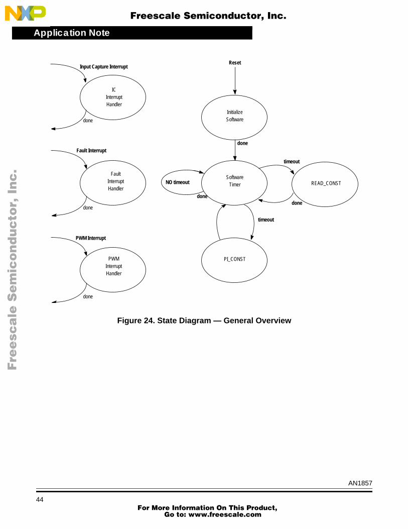
Application Note
F
ree
sca
le S
em
ico
nd
uc
tor,
I
Freescale Semiconductor, Inc.n
c..
.
Figure 24. State Diagram — General Overview
Input Capture Interrupt
ICInterruptHandler
done
Fault Interrupt
FaultInterruptHandler
PWM Interrupt
PWMInterruptHandler
done
done
Reset
InitializeSoftware
done
NO timeout
done
SoftwareTimer
PI_CONST
READ_CONST
done
timeout
timeout
AN1857
44 For More Information On This Product,
Go to: www.freescale.com

Application NoteSoftware
F
ree
sca
le S
em
ico
nd
uc
tor,
I
Freescale Semiconductor, Inc.n
c..
.
READ_CONST is accessed from the main software timer in READ_CONSTrate. The following sequence is performed. See Figure 25READ_CONST:
• All the inputs are scanned (speed pot, start/stop switch,forward/reverse switch, temperature, dc bus current). dc busvoltage is measure in AD interrupt routine.
• The speed command is calculated according to the operationalmode.
• The dc bus voltage is compared with the overvoltage limit andovercurrent flag is checked.
• In case of a fault condition, the fault recovery routine is enteredand until the recovery time expires; the drive remains disabled.
• Finally, the LED driver controls individual LEDs according to thestatus of the drive.
• The PFC hardware is enabled/disabled according to the drivestatus.
• PC-Master commands are serviced.
AN1857
45 For More Information On This Product,
Go to: www.freescale.com
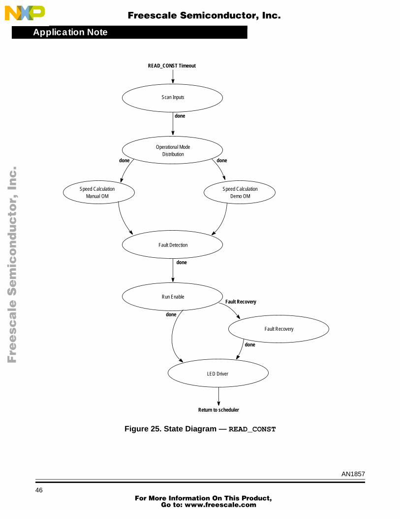
Application Note
F
ree
sca
le S
em
ico
nd
uc
tor,
I
Freescale Semiconductor, Inc.n
c..
.
Figure 25. State Diagram — READ_CONST
READ_CONST Timeout
Scan Inputs
Speed Calculation
done
Operational ModeDistribution
done done
done
done
done
Fault Recovery
Return to scheduler
Manual OMSpeed Calculation
Demo OM
Fault Detection
Run Enable
Fault Recovery
LED Driver
AN1857
46 For More Information On This Product,
Go to: www.freescale.com

Application NoteSoftware
F
ree
sca
le S
em
ico
nd
uc
tor,
I
Freescale Semiconductor, Inc.n
c..
.
PI_CONST is accessed from the main software timer in PI_CONST rate.The rate defines the time constant of the PI controller. The followingsequence is performed (see Figure 26):
1. During deceleration, the dc-bus voltage is checked, and, in caseof overvoltage, the deceleration is interrupted until the capacitor isdischarged.
2. When no deceleration overvoltage is measured, theacceleration/deceleration speed profile is calculated.
3. The actual motor speed is calculated. It is based on the timemeasurement between two subsequent rising edges of the inputcapture.
4. The PI speed controller is performed and the corrected motorfrequency calculated.
The corresponding voltage amplitude is calculated according to the volt-per-hertz profile. Thus, both parameters for PWM generation areavailable (Table_inc, Amplitude).
AN1857
47 For More Information On This Product,
Go to: www.freescale.com
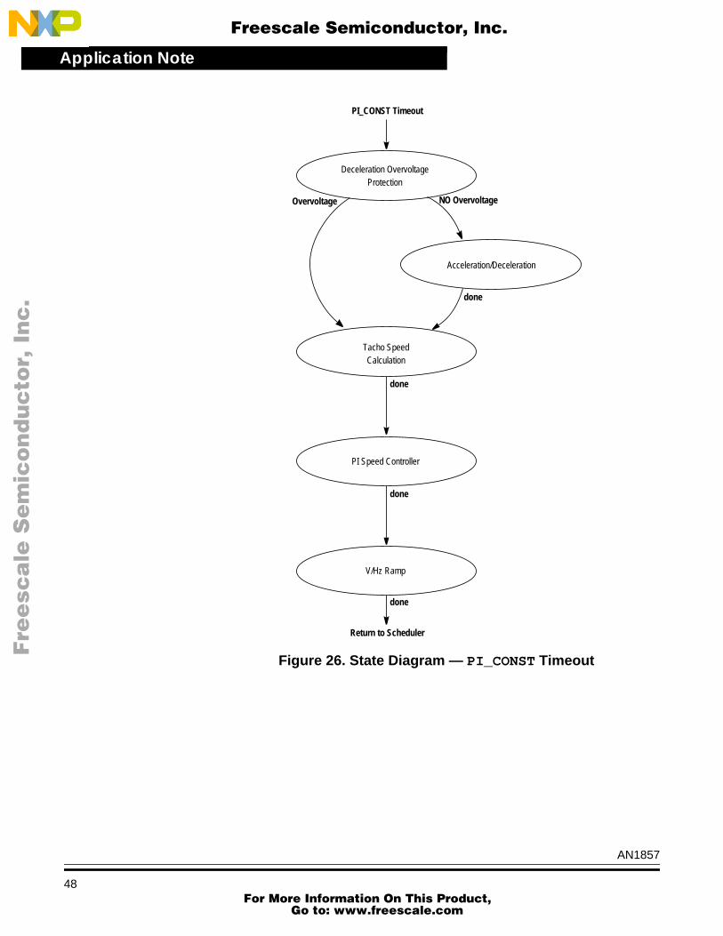
Application Note
F
ree
sca
le S
em
ico
nd
uc
tor,
I
Freescale Semiconductor, Inc.n
c..
.
Figure 26. State Diagram — PI_CONST Timeout
Overvoltage
Deceleration Overvoltage
done
done
done
done
NO Overvoltage
Protection
PI_CONST Timeout
Acceleration/Deceleration
Tacho SpeedCalculation
PI Speed Controller
V/Hz Ramp
Return to Scheduler
AN1857
48 For More Information On This Product,
Go to: www.freescale.com

Application NoteSoftware
F
ree
sca
le S
em
ico
nd
uc
tor,
I
Freescale Semiconductor, Inc.n
c..
.
Software Files The software consists of the following parts:
MAIN.C — MAIN.C is the entry point following a reset and after initialstartup code. It contains the initialization software state code, the mainstate machine with the software timer state code.
SPEED.C — SPEED.C contains READ_CONST code (scan inputs state;operational mode distribution state; speed calculation, manualoperational mode state, speed calculation; PC-Master operation modestate; fault detection state; run enable state; fault recovery state; LEDdriver state; PFC enable/disable logic).
RAMP.C — RAMP.C contains code for acceleration and decelerationrampstate, V/Hz ramp state.
PI.C — PI.C contains PI_CONST timeout code (deceleration overvoltageprotection state, tacho speed calculation state, PI speed controller state,and calls acceleration/deceleration ramp state and V/Hz ramp stateappropriately).
FAULT.C — FAULT.C contains the fault interrupt service routine.
PWMCALC.C — PWMCALC.C contains code to service the PWMinterrupts which ultimately generate the sine outputs to the power stage.
TACHO.C — TACHO.C contains timer A channel 0 interrupt code thatcalculates the time between tachometer interrupts.
MR_IDENT.C — MR_IDENT.C contains code that communicates withthe MC68HC705JJ7 microcontrollers, resident on the optoisolation andpower boards. The resulting information from this routine is used forconfiguration checking and input to system run time parameters.
DigitPFC.C — DigitPFC.C contains software used to drive the powerfactor correction hardware resident on the power board. The softwaresets the duty cycle of timer B channel 0 that pulse-width modulates thepower board’s PFC input hardware at 125 kHz.
RAM.C — The file RAM.C contains the global RAM variable definitionsfor system’s MR32 software.
AN1857
49 For More Information On This Product,
Go to: www.freescale.com

Application Note
F
ree
sca
le S
em
ico
nd
uc
tor,
I
Freescale Semiconductor, Inc.n
c..
.
Code_ISR.C — CODE_ISR.C contains the interrupt and reset vectoraddresses for the system’s MR32 software.
SCI.C — SCI.C contains the PC-Master SCI communication routinescode.
RAM.H — The header file RAM.H contains the global RAM variabledeclarations for the system’s MR32 software.
CONST.H — The header file CONST.H contains the global systemconstants definitions for system’s MR32 software.
CODE_FUN.H — The header file Code_fun.H contains the prototypesof the external functions.
3RDHQUAD.H — The header file 3RDQUAD.H contains a 256-wordone-quadrant sine table with third harmonic injection.
SCI.H — SCI.H contains the PC-Master SCI communication constantand variables declarations.
MR24_VHz_PFC.prm — The parameter file MR24_VHz_PFC.prmcontains the interrupt and reset vector addresses for the system’s MR32software.
AN1857
50 For More Information On This Product,
Go to: www.freescale.com

Application NoteConclusion
F
ree
sca
le S
em
ico
nd
uc
tor,
I
Freescale Semiconductor, Inc.n
c..
.
Conclusion
This application note describes the design of a 3-phase ac speed-controlled induction motor with power factor correction and optionalPC-Master communication software. The controller, optoisolation, andpower boards used in this design are part of Motorola’s tool set and canbe purchased from Motorola. The tool set enables the MR32 to beevaluated in a system without the necessity of building prototypehardware.
The design described in this application note illustrates the efficiencyand simplicity of using the MR32 microcontroller as the processing heartof a robust motor control system for low-cost industrial and consumermotor control applications.
AN1857
51 For More Information On This Product,
Go to: www.freescale.com

N
ON
-D
IS
CL
OS
UR
E
AG
RE
EM
EN
T
RE
QU
IR
ED
Application Note
F
ree
sca
le S
em
ico
nd
uc
tor,
I
Freescale Semiconductor, Inc.n
c..
.
For More Information On This Product,
Go to: www.freescale.com