a 50nw voltage monitor scheme for minimum energy sensor ... · a 50nw voltage monitor scheme for...
TRANSCRIPT

A 50nW Voltage Monitor Scheme for MinimumEnergy Sensor Systems
Anand Savanth1,2, Alex Weddell1, James Myers2, David Flynn1,2, Bashir-Al-Hashimi11Electronics and Computer Science, University of Southampton, UK
2ARM Ltd., Cambridge, UKEmail: [email protected]
Abstract—Small, low-cost and energy efficient wireless sensornodes (WSNs) form a vital part of the Internet of Things (IoT).WSNs spend the majority of their time in low-power sleep modeand wake up for short intervals. To ensure minimum energy(MinE) operation of such sensor nodes, fast wide-range voltagescaling is required. As voltage is aggressively scaled betweenultra-low retention levels and sub, near or super-threshold activelevels, monitoring circuits become essential to guarantee safeoperation of the system. This work demonstrates a 50nW voltagemonitor fabricated as part of the power management unit(PMU) of a 65nm MinE WSN. Ultra low power operation isachieved by duty-cycling the comparators. Further, dynamicpower-bandwidth balancing results in lower quiescent powerwithout loss of response speed. Measured results show 6µsresponse time giving a superior power-delay balance comparedto prior works. This paper describes the design, implementationand measured results along with system implications of the designchoices.
I. INTRODUCTION
Recent works have demonstrated CPU-system designs thatcan operate at supply voltages below transistor thresholdvoltages (sub-550mV) [1][2][3][4]. This allows minimum en-ergy (MinE) operation which is ideal for many emergingsensor applications [5][6][7]. Such sensors are severely energyconstrained and have low activity rates with relatively lowerperformance requirements than is offered by current technol-ogy nodes at nominal voltages. Many of these applications canalso harvest energy from their environment giving theoreticallyunlimited lifetimes [8][9].
A common objective of MinE CPU-systems is to minimizeleakage because WSNs spend the majority of their time insleep modes. Leakage energy also increases exponentially atlow voltages, further degrading total energy. To minimizeleakage fine-grained power gating is used with example sys-tems having as many as 14 power domains [4]. Integratedvoltage regulators (IVRs) are another common feature of MinECPU-systems to: 1) obtain the low voltages required for sub-threshold operation because battery voltages are 1.2V or higherand 2) reduce latency during sleep and active mode transitions.An 80µs sleep-active-sleep transition is demonstrated in [4].
Fast wide-range dynamic voltage scaling (DVS) is desirablein WSNs to enable frequent entry into sleep modes and also tomaximize sleep time. Enabling the clock to the CPU-systemupon wake-up requires careful consideration. An early enablecan cause timing violations and is catastrophic, while a de-
layed enable defeats ultra low power (ULP) operation. Voltagemonitors are thus required to guarantee safe regulator voltage(VREG) levels before the clock is enabled. The proposed designdemonstrates an ULP voltage monitor scheme using: 1) Dutycycled comparators with dynamic hysteresis tuning. 2) Run-time power-bandwidth trade-off to reduce active power. 3)State-aware tuning to provide 6µs response speed.
The next section describes the system with the voltagemonitor highlighting key design metrics. The design andimplementation of the proposed voltage monitor scheme isexplained in section III. Measured results are presented andcompared with prior-art in section IV and conclusions aredrawn in section V.
II. SYSTEM DESCRIPTION
The PMU and CPU-system interface can be reliably timedby the PMU clock if the interaction is limited to clockand/or power gating. With dynamic voltage and frequencyscaling however, voltage settling and clock-locking introducesadditional delays during mode changes. Since WSNs usingMinE CPU-systems operate at frequencies not exceeding tensof MHz [10], clock settling is relatively deterministic. Voltagesettling can have a greater degree of uncertainty becauseintegrated switched capacitor converters in MinE systems canhave higher output impedance compared to linear regulators.Fig. 1a shows the PMU interface with a CPU-system andvoltage monitor. Under ideal conditions, (Fig. 1b) the CPU-system asserts voltage change request (CHV) when a modechange is desired. This is captured by the PMU state-machineand CPU-system clock is disabled (CKEN). The IVR settingis then changed to the requested value while de-assertingthe ACK signal. Assuming the system rail voltage settlesimmediately, CKEN is asserted followed by ACK. The CPU-system resumes in the requested mode and CHV is de-asserted.No monitoring scheme is necessary.
In practice however, the transition time (TCH) is muchlonger, being dominated by the voltage settling time (TVS)and the time it takes for the monitor to detect an in-rangecondition (TVMON). This is illustrated in Fig. 2. It is desirableto minimize TVS and TVMON. TVS is affected by load currentwhich is sensitive to temperature, process and system work-loads and IVR design characteristics such as output impedanceand on/off-chip decoupling capacitance. The objective of thiswork is to minimize TVMON.

MinE CPU
system
Voltage
RegulatorVoltage
monitor
PMU state-
machine
Clock Gen
PMU- Always ON VBAT Domain
VR
EG
1
4
(a)
3
2
CHV (1)
CKEN (2)
IVR (3)
ACK (5)
VREG
a i
b h
c
d g
e f
(b)
5
CKPMU
VBAT
Fig. 1. Voltage monitoring (a) PMU interface block diagram and (b) ideal mode transition waveforms during dynamic voltage scaling.
CHV (1)
CKEN (2)
IVR (3)
ACK (5)
QINRANGE (4)
VREG
TCH
TVS TVMON
Fig. 2. Mode transition waveforms in the presence of non-ideal regulatorcharacteristics
Voltage monitors typically use comparators with factory-trimmed threshold voltages for detecting an unsafe rail voltagecondition. Sensing slow rising or non-monotonic rail voltagescan cause oscillations as rail voltage approaches threshold volt-age. This is overcome by using two comparators with slightlyoffset threshold voltages [11][12]. This two-level monitoringadds hysteresis to the comparator but allows only for a low-voltage unsafe condition to be monitored. In MinE systemshowever, it is necessary to independently monitor for over-voltage conditions as excess leakage can adversely affect MinEoperation. In the conventional scheme this would require fourcomparators making monitoring an energy expensive task.
Monitoring may be implemented with either continuous-time comparators [12] or clocked comparators [13].Continuous-time comparators exhibit fast response speed butat the expense of higher quiescent power and having fourcomparators (for upper and lower thresholds) in the always-ON PMU domain can be particularly detrimental to MinEWSNs. Clocked comparators have relatively lower quiescentpower but suffer from overheads of having to generate adedicated clock. Leakage based oscillators with thyristor-likegain stages have been used to generate comparator clockto reduce these overheads but at the expense of speed [3][13]. This slow clock results in increase in TVMON which isundesirable for fast DVS.
III. PROPOSED DESIGN AND IMPLEMENTATION
The proposed scheme uses reference tuning to add hystere-sis, allowing both upper and lower limits to be monitoredusing two comparators. Figure 3 shows the schematic ofthe proposed voltage monitor. The comparators and thresholdvoltage generators can be power gated using PGEN signal.
TU
TL
÷
TUSEL
TLSEL
BUSEL
BLSEL
FB2
VREG
PGEN nPGENQU
QL
nPGEN
0
1
nPGEN
CMPU
CMPL
VTL
VTU
VREGINT
HVT
Fig. 3. Proposed voltage monitor scheme
This minimizes static power when the voltage monitor ispower gated (system deep-sleep mode). In this mode, the IVRis OFF and hence the monitoring circuit too can be powereddown. The upper and lower comparison thresholds (VTU andVTL) can be programmed using TUSEL and TLSEL. Thetunable range between VTU and VTL covers the entire DVSrange of the MinE CPU-system. The key feature of this workis the bias current selection bits (BUSEL and BLSEL) for bothupper and lower comparators (CMPU and CMPL). The biasselection bits are exercised in a manner so as to minimize thequiescent power of the voltage monitor without compromisingmonitoring speed.
Fig. 4 shows ideal response of the voltage monitor forvarying VREG levels. For sake of simplicity VREG is shown tostart at a voltage below VTL. The outputs QU and QL are bothhigh and QINRANGE is de-asserted indicating an out-of-range or
VTU
VTL
1
2
4
3
QINRANGE
VREG
ΔVTU
programmable
thresholds
QL
QU
VCOMP
ΔVTL
Fig. 4. Conceptual voltage monitor response for varying VREG

TABLE ISUMMARY OF COMPARATOR BIAS CONFIGURATIONS
State CMPU CMPL ∆VTU ∆VTL
1 0 0 - -
2 0 3 - +∆V
3 1 2 +∆V -∆V
4 3 0 -∆V -
unsafe condition for enabling CPU clock. In this state (1) bothcomparators are OFF. As VREG starts rising (state (2)) the firstevent is triggered when VREG > VTL. This event is signalled byCMPL. Thus the PMU can power-down CMPU until this eventoccurs thus reducing the voltage monitor quiescent power.Once VREG is within the desired limits, state (3), both CMPUand CMPL are turned ON but in a low-bandwidth mode soas to satisfy µs order detection of an out-of-range condition.When VREG exceeds VTU, state (4), CMPL is powered downas the trigger can be reliably generated by CMPU when VREGdrops below VTU. By exploiting current-state awareness in thePMU the proposed scheme helps minimize quiescent power inthe voltage monitoring circuit.
Note that state (3)-(2) transition can be fatal to the systemwhile a (3)-(4) transition is less critical. The CPU-systemremains functional in state (4) but potentially at a much higherenergy cost. Therefore in state (3) CMPU quiescent currentis further reduced. The proposed scheme allows three biascurrent settings to be dialled into the comparators. A BxSELsetting of ‘3’ provides fastest response at highest quiescentpower and a setting of ‘1’ provides lowest power operation.Table I summarizes the bias configuration for each state ashighlighted in Fig. 4.
Hysteresis may be added depending on the correspondingcomparator output as described in [13]. The proposed designrelies on TxSEL bits for achieving this. Thus state (2)-(3)transition is at VTL plus a small voltage (∆V) while a (3)-(2)transition is at VTL-∆V. Similarly (3)-(4) occurs at VTU+∆Vand (4)-(3) at VTU-∆V thus preventing any oscillations. Thisis indicated in Table I as ∆VTU and ∆VTL.
A. Comparator
Fig. 5 shows the schematic of the comparator. The tail-current transistor is a thick gate oxide (TGO) device to allowfor better VBIAS control of tail-current. The bias selectionbits effectively change the mirror ratio between M17 and M6controlling response speed of the comparator and its quiescentcurrent. A stack of 6 diode-connected regular-VT transistors(M11-M17) is used for bias generation. Comparators forsensing low voltages use of PMOS input transistors to improvethe gain in the input stage [13] which affects quiescent power.The input differential pair (M4, M5) in the proposed designuse NMOS transistors and the lack of gain is compensated byusing large low-VT devices. This allows input voltages as lowas 0.2V to be sensed reliably. The output of the differentialstage drives an inverter with stacked high-VT devices (M8-M10) which limits short-circuit current and helps reduce power
M10
BSEL
VT VREGINT
nPGEN
nPGEN
Q
VBIAS
M01
M03M02
M05M04
M06
M07
M09
M08
M11
M17
HVT
TGO
M12
0
3
Fig. 5. Comparator schematic
V
t
100mVVT
VREGINT
Q
Tqr
Tqf
Response speed = avg(Tqr,Tqf)
Bias setting 3
Bias setting 2
Bias setting 1
1
10
100
1000
10000
100000
1 1.05 1.1 1.15 1.2 1.25 1.3 1.35 1.4
Re
spo
nse
sp
ee
d (
ns)
Supply Volatge (V)
Bias setting 3
Bias setting 2
Bias setting 1
1
10
100
1000
10000
100000
0 10 20 30 40 50 60 70 80 90 100
Res
po
nse
sp
eed
(n
s)
Temperature (deg C)
T=25°C
V=1.2V
(b)
(a)
(c)
Fig. 6. Comparator simulation results (a) measurement setup, (b) responsespeed vs supply voltage and (c) speed vs temperature for different bias settings
[12]. M1 and M7 allow the comparator to be power gated withQ forced high.
Fig. 6 shows simulation results for supply voltage of 1.0-1.4V and temperature range of 0 - 100C. Response speed ismeasured as the average delay (Fig. 6a) for a correct transitionon Q for change in VREGINT from VT-100mV to VT+100mV[14]. Fig. 6b shows the comparator response speed against

1.E-03
1.E-02
1.E-01
1.E+00
1.E+01
1.E+02
1.E+03
1.E+04
1.E+05
ns /°C ns /V
Bias setting 3
Bias setting 2
Bias setting 1 2000x
20000x
Fig. 7. Comparator simulation results - sensitivity of response speed tosupply voltage and temperature for different bias settings
supply voltage variation (T=25C). Fig. 6c shows the responsespeed with varying temperature. At sufficiently large tailcurrents the comparator speed is less affected by temperature.Both speed and quiescent power increase exponentially withbias setting. So speed can be traded with power. Anotherconsequence of reducing power is the increased sensitivityof comparator speed to voltage and temperature. Simulationresults (Fig. 7) show a 20,000x increase in sensitivity withtemperature and 2,000x increase for voltage. However, sincethe design relies on using low bias current modes only whencomparator response is less critical or is not needed, thisincreased sensitivity does not affect system active-sleep-activetransitions.
B. Threshold Voltage Generator and Divider
Threshold voltage for the comparators is generated usingstacked diode-connected transistors [15] as shown in Fig. 8.Both VTU and VTL are obtained from the lower half of thestack to give identical behaviour as temperature varies. Fora nominal supply voltage of 1.2V all transistors in the stackoperate in sub-threshold regime. PMOS devices are used insource-connected isolated N-wells to avoid body effects andease layout. Each node in the divider stack is decoupled using20fF MOS capacitors to provide rejection of high frequencysupply ripple. Further, the ON resistance of the multiplexersand a 120fF capacitance on the output node reduces noise onthe reference node.
20
Stages
nPGEN
MOS
Cap
TV
19
TV
10
TV
8
TV2
TV4
TUSEL
TLSEL
0
6
0
6
VTU
VTL
FB
2
0
1
VREGINT
VREG
nPGEN
(a) (b)
Fig. 8. Schematic of (a) internal threshold voltage generator and (b) voltagedivider
TABLE IISIMULATED SPREAD ON VCOMP AND ∆V
TxSEL 1 2 3 4 5 6
VCOMP (mV) µ 54 48 44 42 41 42σ 4 4 4 3 3 3
∆VTU (mV) µ 45 79 59 44 36 34σ 4 6 5 4 4 3
∆VTL (mV) µ 50 89 68 51 40 33σ 5 6 5 5 4 4
The speed and accuracy of comparison depends on bothcomparator and the threshold voltage generator. The compara-tors use large devices, common-centroid matched layout, guardrings and dummy devices with sufficient distance betweenactive devices and the well edges to minimise well-proximityeffects. Thus contribution of comparator variation to variationin trip points is relatively small. The threshold voltage gen-erator on the other hand uses devices in isolated wells whichare not matched in layout. They are more prone to on-chipvariation. Thus accuracy of comparison is largely determinedby variations in the threshold voltage generator.
Figure 9 shows the variation of threshold voltages (VTU andVTL) for different tap settings over 1000 monte-carlo runs.The worst case spread for VTL is about 60mV and 64mV forVTU. For both VTU and VTL, the box height shows the spreadwith center bar indicating the corresponding mean. For thesame threshold voltage setting VTU and VTL do not overlap-meaning the circuit will always provide a reliable comparisonwindow (VCOMP). This however is a pessimistic result forVCOMP because the minimum of VTU and maximum of VTLdo not occur simultaneously. The mean values for VCOMP andthe corresponding hysteresis (∆V) obtained from simulationsis tabulated in Table II.
Note that for VREG greater than VBAT/2 (approximate), thecomparator sense voltage is divided by 2 using FB2 (Fig. 3).Since the divided version of VREG is obtained at the midpointof the diode stack (Fig. 8), the ratio remains independent oftemperature and VREG.
IV. RESULTS
This section presents measured DC and transient resultsof the proposed scheme. Fig 10 shows DC results for two
1 2 3 4 5 6
0
0.2
0.4
0.6
0.8
1
1.2
0.15
0.20
0.25
0.30
0.35
0.40
0.45
1 2 3 4 5 6
Thre
sho
ld v
olt
age
(V
)
TxSEL bit setting
VTU VTL
Fig. 9. Spread of VTU and VTL over 1000 monte-carlo simulations.
VREG
QU
QL
ΔVTL=220mV
VREG
QU
QL
ΔVTL=5mV
ΔVTU=120mV
(a)
(b)
Fig. 10. Measured DC results showing (a) ∆VTL and (b) ∆VTU for twooperating states (3 and 4 in Fig. 4).
VREG
QLΔVREG=VTL±30mV
6μs
Fig. 11. Meaured transient results showing CMPL speed for a bias settingof 2.
cases: (a) with VREG increasing up to the desired range beforedecreasing and (b) with VREG increasing beyond the desiredrange (over-voltage). Fig. 10a shows a ∆VTL of 220mV. How-ever when VREG exceeds VTU (Fig. 10b) ∆VTL is redundantand is reduced to 5mV. A 120mV ∆VTU prevents QU fromoscillating. Note that QINRANGE is asserted only for VTL <VREG < VTU.
Fig 11 shows the transient results with VREG transitioningfrom VTL-30mV to VTL+30mV. Since this does not exceedVTU, QL determines QINRANGE. Note that the delay in detectingan in-range condition is 6µs (1.2V, room temperature). Fig.12 demonstrates the voltage monitor for system transitionsbetween super, near and sub-threshold voltages. VREG transi-tions from 0.3V retention voltage to 0.4V, 0.6V and 0.8V in10ms. In each mode the voltage monitor correctly detects anin-range and out-of-range condition (upper and lower limits).Note that FB2 is asserted for 0.4V to bypass the divider. Modetransitions at 0.8V are sub-ms order as dictated by higher CPU
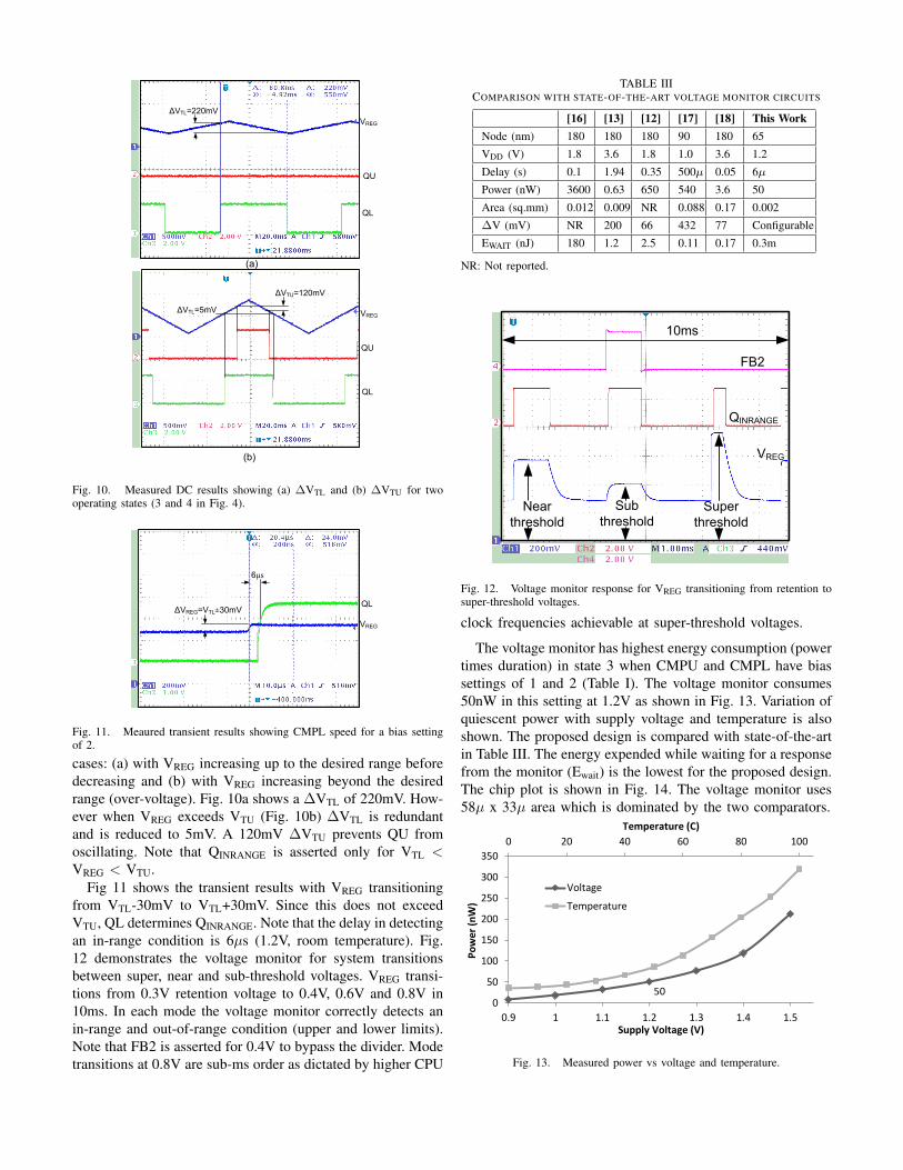
TABLE IIICOMPARISON WITH STATE-OF-THE-ART VOLTAGE MONITOR CIRCUITS
[16] [13] [12] [17] [18] This WorkNode (nm) 180 180 180 90 180 65
VDD (V) 1.8 3.6 1.8 1.0 3.6 1.2
Delay (s) 0.1 1.94 0.35 500µ 0.05 6µ
Power (nW) 3600 0.63 650 540 3.6 50
Area (sq.mm) 0.012 0.009 NR 0.088 0.17 0.002
∆V (mV) NR 200 66 432 77 Configurable
EWAIT (nJ) 180 1.2 2.5 0.11 0.17 0.3m
NR: Not reported.
VREG
QINRANGE
FB2
Super
threshold
Sub
thresholdNear
threshold
10ms
Fig. 12. Voltage monitor response for VREG transitioning from retention tosuper-threshold voltages.
clock frequencies achievable at super-threshold voltages.
The voltage monitor has highest energy consumption (powertimes duration) in state 3 when CMPU and CMPL have biassettings of 1 and 2 (Table I). The voltage monitor consumes50nW in this setting at 1.2V as shown in Fig. 13. Variation ofquiescent power with supply voltage and temperature is alsoshown. The proposed design is compared with state-of-the-artin Table III. The energy expended while waiting for a responsefrom the monitor (Ewait) is the lowest for the proposed design.The chip plot is shown in Fig. 14. The voltage monitor uses58µ x 33µ area which is dominated by the two comparators.
50
0 20 40 60 80 100
0
50
100
150
200
250
300
350
0
50
100
150
200
250
300
350
0.9 1 1.1 1.2 1.3 1.4 1.5
Temperature (C)
Po
wer
(n
W)
Supply Voltage (V)
Voltage
Temperature
Fig. 13. Measured power vs voltage and temperature.

CMPU CMPL DIVIDERVT
58μ
33μ
Fig. 14. Chip Plot.
10-6 10-5 10-4 10-3 10-2 10-1 100 101
Response Speed (s)
10-1
100
101
102
103
104
Pow
er
(nW
)
[16]
[13]
[12]
[17]
[18]
[14]
THISWORK
Fig. 15. Power-Delay balance compared with prior works.
V. CONCLUSION
Scaling supply voltage to sub/near threshold level is neces-sary to achieve minimum energy operation in processors forWSNs. To best exploit potential energy savings, such WSNsneed assist circuits, many of which perform analog functions.This paper described the implementation of an ultra low powervoltage monitor circuit to assist MinE CPU-systems with fastwide-range voltage scaling. The proposed scheme achievesbetter balance between response speed and quiescent poweras shown in Fig. 15.
The benefits from MinE CPU-systems can easily be over-whelmed by slow or high power voltage monitors. For theCPU-system described in [4], leakage power increases from100nW by 16x when VREG changes from 0.3V to 0.8V inpreparation for active mode. The proposed voltage monitorsaves 1.11nJ/wake by reducing the delay to enabling theCPU-system clock by 100x. The voltage monitor thus be-comes energy neutral for sensor workloads with more than50 wakes/second. Duty-cycled comparators and state-awaredynamic power-bandwidth tuning limit the overheads of theproposed monitoring scheme to 1% of the CPU-system activepower at MEP voltage.
ACKNOWLEDGMENT
The authors would like to thank Europractice and themini@sic test silicon fabrication team, as well as researchteam members Bal Sandhu and Pranay Prabhat for usefuldiscussions and reviews.
REFERENCES
[1] J. Kwong, Y. Ramadass, N. Verma et al., “A 65nm Sub-Vt Micro-controller with Integrated SRAM and Switched-Capacitor DC-DC Con-verter,” in Solid-State Circuits Conference, 2008. ISSCC 2008. Digestof Technical Papers. IEEE International, Feb 2008, pp. 318–616.
[2] D. Bol, J. De Vos, C. Hocquet et al., “SleepWalker: A 25-MHz 0.4-VSub-mm2 7µW/MHz Microcontroller in 65-nm LP/GP CMOS for Low-Carbon Wireless Sensor Nodes,” Solid-State Circuits, IEEE Journal of,vol. 48, no. 1, pp. 20–32, Jan 2013.
[3] M. Fojtik, D. Kim, G. Chen et al., “A Millimeter-Scale Energy-Autonomous Sensor System With Stacked Battery and Solar Cells,”Solid-State Circuits, IEEE Journal of, vol. 48, no. 3, pp. 801–813, March2013.
[4] J. Myers, A. Savanth, R. Gaddh et al., “A Subthreshold ARM Cortex-M0+ Subsystem in 65nm CMOS for WSN Applications with 14 PowerDomains, 10T-SRAM, and Integrated Voltage Regulator,” IEEE Journalof Solid-State Circuits, vol. 51, no. 1, pp. 31–44, Jan 2016.
[5] A. Mainwaring, D. Culler, J. Polastre, R. Szewczyk, and J. Anderson,“Wireless Sensor Networks for Habitat Monitoring,” in Proceedings ofthe 1st ACM International Workshop on Wireless Sensor Networks andApplications, ser. WSNA ’02, 2002, pp. 88–97.
[6] K. Chintalapudi, E. A. Johnson, and R. Govindan, “Structural DamageDetection Using Wireless Sensor-Actuator Networks,” in Proceedingsof the 2005 IEEE International Symposium on, Mediterrean Conferenceon Control and Automation Intelligent Control, 2005., June 2005, pp.322–327.
[7] E. S. Biagioni and K. W. Bridges, “The Application Of Remote SensorTechnology To Assist The Recovery Of Rare And Endangered Species,”International Journal of High Performance Computing Applications,vol. 16, p. 2002, 2002.
[8] S. Roundy, P. K. Wright, and J. Rabaey, “A Study of Low LevelVibrations as a Power Source for Wireless Sensor Nodes,” ComputerCommunications, vol. 26, no. 11, pp. 1131 – 1144, 2003, ubiquitousComputing.
[9] S. Escolara, S. Chessab, and J. Carreteroa, “Energy-neutral networkedwireless sensors,” Simulation Modelling Practice and Theory, vol. 43,pp. 1 – 15, 2014.
[10] Y. Pu, X. Zhang, J. Huang et al., “Misleading Energy and PerformanceClaims in Sub/Near Threshold Digital Systems,” in Computer-AidedDesign (ICCAD), 2010 IEEE/ACM international Conference on, Nov2010, pp. 625–631.
[11] Maxim Integrated. (2008) “Microprocessor Voltage Monitorswith Programmable Voltage Detection”. Last accessed July2016. [Online]. Available: https://datasheets.maximintegrated.com/en/ds/MAX8211-MAX8212.pdf
[12] B. Mishra, C. Botteron, G. Tasselli, C. Robert, and P. A. Farine, “ASub-µA Power Management Circuit in 0.18um CMOS for Energy Har-vesters,” in Design, Automation Test in Europe Conference Exhibition(DATE), 2013, March 2013, pp. 1197–1202.
[13] I. Lee, S. Bang, Y. Lee et al., “A 635pW Battery Voltage SupervisoryCircuit for Miniature Sensor Nodes,” in 2012 Symposium on VLSICircuits (VLSIC), June 2012, pp. 202–203.
[14] Maxim Integrated. (2015) “125nA Supervisory Circuits with Capacitor-Adjustable Reset and Watchdog Timeouts”. Last accessed July2016. [Online]. Available: https://datasheets.maximintegrated.com/en/ds/MAX16056-MAX16059.pdf
[15] J. Lee and S. Cho, “A 1.4-µW 24.9-ppm/oC Current Reference WithProcess-Insensitive Temperature Compensation in 0.18-µm CMOS,”IEEE Journal of Solid-State Circuits, vol. 47, no. 10, pp. 2527–2533,Oct 2012.
[16] H. B. Le, X. D. Do, S. G. Lee, and S. T. Ryu, “A Long Reset-TimePower-On Reset Circuit with Brown-Out Detection Capability,” IEEETransactions on Circuits and Systems II: Express Briefs, vol. 58, no. 11,pp. 778–782, Nov 2011.
[17] J. Guo, W. Shi, K. N. Leung, and C. S. Choy, “Power-On-Reset Circuitwith Power-off Auto-Discharging Path for Passive RFID Tag ICs,” in2010 53rd IEEE international Midwest Symposium on Circuits andSystems, Aug 2010, pp. 21–24.
[18] I. Lee, Y. Lee, D. Sylvester, and D. Blaauw, “Low Power BatterySupervisory Circuit with Adaptive Battery Health Monitor,” in 2014Symposium on VLSI Circuits Digest of Technical Papers, June 2014, pp.1–2.