a carrier-based neutral voltage modulation 2014
TRANSCRIPT

IEEE TRANSACTIONS ON INDUSTRIAL ELECTRONICS, VOL. 61, NO. 2, FEBRUARY 2014 625
A Carrier-Based Neutral Voltage ModulationStrategy for Multilevel Cascaded Inverters
Under Unbalanced DC SourcesYounghoon Cho, Member, IEEE, Thomas LaBella, Student Member, IEEE,
Jih-Sheng Lai, Fellow, IEEE, and Matthew K. Senesky, Member, IEEE
Abstract—This paper proposes a pulsewidth-modulation strat-egy to achieve balanced line-to-line output voltages and to maxi-mize the modulation index in the linear modulation range wherethe output voltage can be linearly adjusted in the multilevelcascaded inverter (MLCI) operating under unbalanced dc-linkconditions. In these conditions, the linear modulation range isreduced, and a significant output voltage imbalance may occuras voltage references increase. In order to analyze these effects,the voltage vector space for MLCI is evaluated in detail. Fromthis analysis, the theory behind the output voltage imbalance isexplained, and the maximum linear modulation range consideringan unbalanced dc-link condition is evaluated. After that, a neutralvoltage modulation strategy is proposed to achieve output volt-age balancing as well as to extend the linear modulation rangeup to the maximum reachable point in theory. In the proposedmethod, too large of a dc-link imbalance precludes the balancingof the output voltages. This limitation is also discussed. Both thesimulations and the experiments for a seven-level phase-shiftedmodulated MLCI for electric vehicle traction motor drive showthat the proposed method is able to balance line-to-line outputvoltages as well as to maximize the linear modulation range underthe unbalanced dc-link conditions.
Index Terms—Harmonic injection, multilevel cascaded invert-ers (MLCIs), neutral voltage modulation (NVM), phase-shifted(PS) modulation, space vector pulsewidth modulation (PWM)(SVPWM).
I. INTRODUCTION
MULTILEVEL inverters enable the synthesis of a sinu-soidal output voltage from several steps of voltages. For
this reason, multilevel inverters have low dv/dt characteristicsand generally have low harmonics in the output voltage andcurrent. In addition, the switching of very high voltages canbe achieved by stacking multilevel inverter modules [1]–[5].Due to these advantages, multilevel inverters have been applied
Manuscript received September 2, 2011; revised March 1, 2012 and June 9,2012; accepted August 26, 2012. Date of publication March 21, 2013; date ofcurrent version August 9, 2013.
Y. Cho is with the Department of Electrical Engineering, Konkuk University,Seoul 151-742, Korea (e-mail: [email protected]).
T. LaBella and J.-S. Lai are with the Future Energy Electronics Center,Virginia Polytechnic Institute and State University, Blacksburg, VA 24061-0111USA.
M. K. Senesky is with Texas Instruments Kilby Labs, Santa Clara, CA 95051USA.
Color versions of one or more of the figures in this paper are available onlineat http://ieeexplore.ieee.org.
Digital Object Identifier 10.1109/TIE.2013.2254091
in various application fields [6]–[10]. Among various topolo-gies for multilevel inverters, the multilevel cascaded inverter(MLCI) structure is one of the prominent topologies becauseof its simple structure for modularization and fault-tolerantcapability. Therefore, MLCIs are used for many applications,such as dynamic voltage restorer, static synchronous compen-sator (STATCOM), high-voltage energy storage device, photo-voltaic inverters, medium-voltage drives, electric vehicle (EV)traction drives, and so on [13]–[24]. In MLCI applications, amodulation strategy to generate gating signals is very crucial toachieve high-performance control. Regarding this issue, manystudies have been conducted, and they are roughly categorizedinto multilevel selective harmonic elimination pulsewidth mod-ulation (PWM) (SHEPWM), multilevel carrier-based PWM,and multilevel space vector PWM (SVPWM) methods [4].Generally, a carrier-based PWM or SVPWM is preferred inapplications such as motor drives [15], where dynamic prop-erties are very important, whereas SHEPWM is preferred insome high-power static power conversion applications [11],[12]. In [25], an SVPWM method has been studied to coverthe overmodulation range in the multilevel inverter. To reducethe common-mode voltage, a multilevel SVPWM has beenproposed in [26]. The series SVPWM method has been reportedto easily implement SVPWM for the MLCI [27]. In [28],an SVPWM is proposed for hybrid inverters consisting ofneutral point clamp and H-bridge inverters to improve outputvoltage quality and efficiency. As with two-level inverters, itis also possible to implement carrier-based SVPWMs whichare equivalent to traditional SVPWMs by injecting a commonoffset voltage to the three-phase references [29]–[31]. In [29]–[31], some methods to calculate the offset voltages to achievethe optimal space vector switching sequence are addressed. Theperformances of a carrier-based PWM and an SVPWM arecompared, and a PWM scheme is proposed to obtain an optimaloutput voltage in the multilevel inverter in [31].
On the other hand, MLCIs require separated dc links. There-fore, if there is one or more faults present in the dc links ineach phase, or if the voltage magnitudes of the dc links areunequal, the output voltage of the MLCI can be unbalancedwithout proper compensation. To resolve this issue, some stud-ies have been conducted. In [32], it is shown that the availablemodulation index is reduced under faulty conditions on switchmodules in multilevel inverters, and compensation algorithmsare proposed for phase-disposition PWM and phase-shifted
0278-0046 © 2013 IEEE

626 IEEE TRANSACTIONS ON INDUSTRIAL ELECTRONICS, VOL. 61, NO. 2, FEBRUARY 2014
(PS) PWM cases. For a STATCOM application, a zero sequencevoltage to decouple a three-phase MLCI into three single-phase MLCIs is applied as well as zero average active powertechniques to operate the MLCI under unbalanced source orload conditions [33]. Reference [34] explains why the optimumangles and modulation indexes are necessary to obtain maxi-mum balanced load voltages in the MLCI undergoing a faulton switching modules. A neutral voltage shifting techniquehas been introduced for balancing the state of charge in theMLCI-based battery energy storage system [35]. In [36], a dutycycle modification method has been proposed to compensatean output voltage imbalance caused by single-phase powerfluctuations. Reference [37] has shown that a zero sequencecomponent helps to obtain the maximum balanced output volt-ages in a fault condition. In [38], an offset voltage injectiontechnique is studied to balance the output voltage of the MLCI,but the use of an integrator in the compensation method may re-duce dynamic characteristics in applications such as EV motordrives. Recently, the multilevel multiphase feedforward spacevector modulation technique called MFFSVM is proposed tocompensate the voltage imbalances in MLCIs [39], [45].
In this paper, a carrier-based PWM strategy to balance line-to-line output voltages and to maximize the linear modulationrange where the output voltage can be linearly controlled inthe MLCI operating under unbalanced dc-link conditions isproposed. In unbalanced dc-link conditions, the maximum syn-thesizable voltage in each phase is not uniform. Consequently,the linear modulation range is reduced, and a significant outputvoltage imbalance may occur as output voltage referencesincrease. In order to analyze the imbalance effect, the voltagevector space for the MLCI is evaluated in detail. From thisanalysis, the theory behind the output voltage imbalance is ex-plained, and the maximum linear modulation range consideringunbalanced dc sources is evaluated. After that, a neutral voltagemodulation (NVM) strategy is proposed to achieve output volt-age balancing as well as to extend the linear modulation rangeup to the maximum reachable point in theory. In the proposedmethod, the neutral voltage reference, which considers a zerosequence voltage to compensate the output voltage imbalance,and an offset voltage to extend the linear modulation range areeasily obtained through simple arithmetic calculations. In theproposed method, too large of a dc-link imbalance precludesthe output voltages from being balanced. This limitation is alsodiscussed. In addition, a fault-tolerant operation is naturallycovered, because the MLCI undergoing an unbalanced dc-linkcondition can be considered as an MLCI operating under afaulty condition on switch modules. Compared to the existingmethods, the proposed strategy is very simple to implement,compensates the output voltage imbalance in real time, andmaximizes the voltage utilization of the dc links. Therefore, ifthis scheme is applied to applications such as EV traction drivesystems, the dynamic characteristics can be greatly improved.
This paper is organized as follows. In Section II, the volt-age vector space for the one-by-three configuration MLCI isanalyzed for a conceptual study. The proposed modulationstrategy is addressed in Section III. In Sections IV and V, thesimulations and the experimental results on the two-by-threeMLCI are presented. Section VI concludes this paper.
Fig. 1. MLCI-based inverter for EV traction drive.
II. SYSTEM CONFIGURATION AND VOLTAGE VECTOR
SPACE ANALYSIS
A. Configuration of MLCI for EV Traction Motor Drive
Fig. 1 shows the EV traction motor drive system that is dealtwith in this paper. In this configuration, various power ratingscan be easily implemented by configuring the number of thesingle H-bridge modules according to a required specificationsuch as a neighborhood EV, full-size sedan, and so on. Here,each H-bridge module incorporates voltage and current sensingcircuitries, gate drivers, and communication interfaces betweenthe module itself and the main controller. In addition, batterycells can be also included in the H-bridge module. The unipolarmodulation technique is applied between two switching legs inthe H-bridge module. Consequently, the effective switching fre-quency in each H-bridge module is twice the carrier frequency.In addition to this, the well-known PS modulation technique isused to implement interleaving and multilevel operation [40]–[42]. Therefore, the effective switching frequency fsw in aphase is
fsw = 2N × fc (1)
where N and fc represent the number of the H-bridge modulesin each phase and the carrier frequency of PWM, respectively.As an example, Fig. 2 shows the carriers for each module,the duty cycles in unipolar modulation, and the output voltagewhen N = 2.
B. Voltage Vector Space Analysis
When the dc-link voltage of a single H-bridge module is Vdc,the output voltage vpn has three states, i.e., Vdc, 0, and −Vdc,

CHO et al.: CARRIER-BASED NVM STRATEGY FOR MLCIs UNDER UNBALANCED DC SOURCES 627
Fig. 2. Unipolar and phase shift modulation for single H-bridge module.
Fig. 3. Output voltage of a single H-bridge module.
Fig. 4. One-by-three configuration MLCI.
as shown in Fig. 3. By adopting the concept of a switchingfunction, it can be represented as
vpn =SpVdc
Sp ∈{−1, 0, 1}p=a,b,or,c (2)
where Sp is a switching function and p can be replaced with a,b, or c, which represent the phases.
Fig. 4 shows a simple one-by-three configuration MLCI. Forvoltage vector space analysis, the main concept is derived fromthis simple topology, and then, it is expanded to more levels. InFig. 4, there are two neutral points s and n in the MLCI. Here,the voltage between the output point of each phase and theneutral point n is defined as the pole voltage. The pole voltagesare represented as van, vbn, and vcn. The voltage between theoutput point of each phase and the load side neutral point s isspecified as the phase voltage. The phase voltages include vas,vbs, and vcs. By using this concept, the voltage between the twoneutral points is defined as vsn and can be written as
vsn = −vas + van = −vbs + vbn = −vcs + vcn. (3)
By using the condition that the sum of all phase voltages is zerobecause the load does not have a neutral line, vsn is rewritten as
vsn =1
3(van + vbn + vcn). (4)
Fig. 5. Voltage vector space of one-by-three configuration MLCI.
By substituting (4) into (3), the phase voltage of each phase isrepresented as follows by using the relationship defined in (2):
vas =2
3SaVdc_a −
1
3SbVdc_b −
1
3ScVdc_c
vbs = − 1
3SaVdc_a +
2
3SbVdc_b −
1
3ScVdc_c
vcs = − 1
3SaVdc_a −
1
3SbVdc_b +
2
3ScVdc_c. (5)
If the magnitudes of three dc links are balanced so that Vdc_a,Vdc_b, and Vdc_c have the same value Vdc, the voltage vectorspace in α−β coordinates is defined in Fig. 5(a) by using (5).In the figure, underbars indicate that the switching function hasthe value of −1. A part of the hexagon in Fig. 5(a) is shownin Fig. 5(b). In this figure, the vectors v010 and v111 are placedat the same reference axis, phase b. However, the constituentsof those vectors are different. For v010, this vector can besynthesized without the other two phases’ assistance. However,v111 cannot be produced without other vectors according to (5).From this, let the vectors which do not require other two phases’assistance to be defined as “the independent vectors.” Similarly,the vectors which require other phases’ support are defined as“the dependent vectors.” According to these definitions, v100,v001, and v010 are the independent vectors, while v111, v111,and v111 are the dependent vectors in Fig. 5(b). Fig. 5(a) alsocompares the regions that can be composed by the independent
628 IEEE TRANSACTIONS ON INDUSTRIAL ELECTRONICS, VOL. 61, NO. 2, FEBRUARY 2014
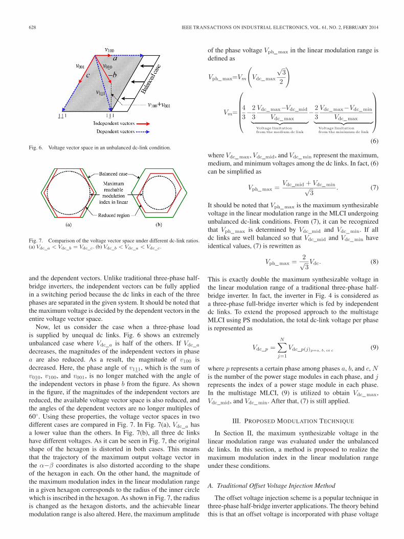
Fig. 6. Voltage vector space in an unbalanced dc-link condition.
Fig. 7. Comparison of the voltage vector space under different dc-link ratios.(a) Vdc_a < Vdc_b = Vdc_c. (b) Vdc_b < Vdc_a < Vdc_c.
and the dependent vectors. Unlike traditional three-phase half-bridge inverters, the independent vectors can be fully appliedin a switching period because the dc links in each of the threephases are separated in the given system. It should be noted thatthe maximum voltage is decided by the dependent vectors in theentire voltage vector space.
Now, let us consider the case when a three-phase loadis supplied by unequal dc links. Fig. 6 shows an extremelyunbalanced case where Vdc_a is half of the others. If Vdc_adecreases, the magnitudes of the independent vectors in phasea are also reduced. As a result, the magnitude of v100 isdecreased. Here, the phase angle of v111, which is the sum ofv010, v100, and v001, is no longer matched with the angle ofthe independent vectors in phase b from the figure. As shownin the figure, if the magnitudes of the independent vectors arereduced, the available voltage vector space is also reduced, andthe angles of the dependent vectors are no longer multiples of60◦. Using these properties, the voltage vector spaces in twodifferent cases are compared in Fig. 7. In Fig. 7(a), Vdc_a hasa lower value than the others. In Fig. 7(b), all three dc linkshave different voltages. As it can be seen in Fig. 7, the originalshape of the hexagon is distorted in both cases. This meansthat the trajectory of the maximum output voltage vector inthe α−β coordinates is also distorted according to the shapeof the hexagon in each. On the other hand, the magnitude ofthe maximum modulation index in the linear modulation rangein a given hexagon corresponds to the radius of the inner circlewhich is inscribed in the hexagon. As shown in Fig. 7, the radiusis changed as the hexagon distorts, and the achievable linearmodulation range is also altered. Here, the maximum amplitude
of the phase voltage Vph_max in the linear modulation range isdefined as
Vph_max=Vm
(Vdc_max
√3
2
)
Vm=
⎛⎜⎜⎜⎜⎝4
3−2
3
Vdc_max−Vdc_mid
Vdc_max︸ ︷︷ ︸Voltage limitationfrom themedium dc link
−2
3
Vdc_max−Vdc_min
Vdc_max︸ ︷︷ ︸Voltage limitationfrom theminimumdc link
⎞⎟⎟⎟⎟⎠(6)
where Vdc_max, Vdc_mid, and Vdc_min represent the maximum,medium, and minimum voltages among the dc links. In fact, (6)can be simplified as
Vph_max =Vdc_mid + Vdc_min√
3. (7)
It should be noted that Vph_max is the maximum synthesizablevoltage in the linear modulation range in the MLCI undergoingunbalanced dc-link conditions. From (7), it can be recognizedthat Vph_max is determined by Vdc_mid and Vdc_min. If alldc links are well balanced so that Vdc_mid and Vdc_min haveidentical values, (7) is rewritten as
Vph_max =2√3Vdc. (8)
This is exactly double the maximum synthesizable voltage inthe linear modulation range of a traditional three-phase half-bridge inverter. In fact, the inverter in Fig. 4 is considered asa three-phase full-bridge inverter which is fed by independentdc links. To extend the proposed approach to the multistageMLCI using PS modulation, the total dc-link voltage per phaseis represented as
Vdc_p =
N∑j=1
Vdc_p(j)p=a, b, or c(9)
where p represents a certain phase among phases a, b, and c, Nis the number of the power stage modules in each phase, and jrepresents the index of a power stage module in each phase.In the multistage MLCI, (9) is utilized to obtain Vdc_max,Vdc_mid, and Vdc_min. After that, (7) is still applied.
III. PROPOSED MODULATION TECHNIQUE
In Section II, the maximum synthesizable voltage in thelinear modulation range was evaluated under the unbalanceddc links. In this section, a method is proposed to realize themaximum modulation index in the linear modulation rangeunder these conditions.
A. Traditional Offset Voltage Injection Method
The offset voltage injection scheme is a popular technique inthree-phase half-bridge inverter applications. The theory behindthis is that an offset voltage is incorporated with phase voltage

CHO et al.: CARRIER-BASED NVM STRATEGY FOR MLCIs UNDER UNBALANCED DC SOURCES 629
Fig. 8. Implementation of the NVM method.
references to implement various PWM schemes in carrier-basedPWM by using the fact that line-to-line voltages are applied toa three-phase load [43], [44]. For example, the offset voltagev∗sn is injected to the phase voltage references v∗as, v∗bs, and v∗csto implement carrier-based SVPWM as in
v∗sn =v∗max + v∗min
2v∗max = max (v∗as, v
∗bs, v
∗cs)
v∗min = min (v∗as, v∗bs, v
∗cs) . (10)
Then, the pole voltage references v∗an, v∗bn, and v∗cn, which willbe converted to PWM duty references, are
v∗an=v∗as−v∗sn v∗bn=v∗bs−v∗sn v∗cn=v∗cs−v∗sn. (11)
However, the aforementioned technique may not maximizethe linear modulation range in MLCI undergoing unbalanceddc-link conditions.
B. Proposed NVM Method
If the dc links in an MLCI are unbalanced and the traditionaloffset voltage injection methods are utilized, the three-phaseoutput voltages may become distorted as the phase voltagereference approaches Vph_max. This is because the traditionalmethods are not considering unbalanced dc-link conditions.Therefore, even if a phase can synthesize an output voltagereference in the linear modulation range, the other phases can besaturated or go into the overmodulation region. In this situation,a neutral voltage can be produced by the saturated or overmod-ulated phase. In order to resolve this issue and to synthesize theoutput voltage to Vph_max in the linear modulation range,the NVM technique is proposed in this paper. Fig. 8 showsthe concept of the proposed NVM technique. Here, a neutralvoltage between the two neutral points n and s in Fig. 4 ismodulated to compensate the output voltage imbalance causedby unbalanced dc-link conditions. To do this, first, the weightconstant Kw is defined as
Kw =Vdc_mid + Vdc_min
2. (12)
By using (12), the weight factors are calculated as
Kw_a=Kw
Vdc_aKw_b=
Kw
Vdc_bKw_c=
Kw
Vdc_c(13)
where Kw_a, Kw_b, and Kw_c represent the weight factorsfor phases a, b, and c, respectively. Next, the weight factorsare multiplied by the phase voltage references, and the newreferences v′as, v′bs, and v′cs are obtained as
v′as=Kw_av∗as v′bs=Kw_bv
∗bs v′cs=Kw_cv
∗cs. (14)
It should be noted that, depending on dc-link conditions, thesum of v′as, v′bs, and v′cs may not be zero. By using thesecomponents, the injected voltage v′sn and the pole voltagereferences are given as
v′max = max (v′as, v′bs, v
′cs) v′min = min (v′as, v
′bs, v
′cs)
v′sn =v′max + v′min
2
⎡⎣ v∗anv∗bnv∗cn
⎤⎦ =
⎡⎣ v∗as − v′snv∗bs − v′snv∗cs − v′sn
⎤⎦ . (15)
From (15), the line-to-line voltages across each phase of theload are represented as⎡
⎣ v∗abv∗bcv∗ca
⎤⎦ =
⎡⎣ v∗an − v∗bnv∗bn − v∗cnv∗cn − v∗an
⎤⎦ ==
⎡⎣ v∗as − v′sn − v∗bs + v′snv∗bs − v′sn − v∗cs + v′snv∗cs − v′sn − v∗as + v′sn
⎤⎦
=
⎡⎣ v∗as − v∗bsv∗bs − v∗csv∗cs − v∗as
⎤⎦ . (16)
As it can be seen in (16), v′sn does not appear in the line-to-line voltages, and it is still considered as a hidden freedom ofvoltage modulation. Now, let us consider the role of the weightfactors Kw_a, Kw_b, and Kw_c, which are inversely propor-tional to the corresponding dc-link voltage. For convenience, letus assume that the magnitudes of the dc-link voltage are underthe following relationship:
Vdc_a < Vdc_b < Vdc_c. (17)
Then, from (13) and (17)
Kw_a >Kw_b > Kw_c Kw_a > 1
Kw_b,Kw_c < 1. (18)
Equation (18) gives
|v′as| > |v∗as| |v′bs| < |v∗bs| |v′cs| < |v∗cs| . (19)
From (15) and (19), it can be recognized that, if v′as, whosedc-link voltage is less than the others, is corresponding to v′max
or v′min, the absolute value of v′sn is greater than v∗sn in (10).On the other hand, the final pole voltage references v∗an, v∗bn,and v∗cn are calculated by subtracting v′sn from the originalphase voltage references v∗as, v∗bs, and v∗cs as in (15). From thisreasoning, in this example, it is supposed that, if v′as is corre-sponding to v′max, then the final pole voltage references v∗an,v∗bn, and v∗cn are less than the original pole voltage references
630 IEEE TRANSACTIONS ON INDUSTRIAL ELECTRONICS, VOL. 61, NO. 2, FEBRUARY 2014
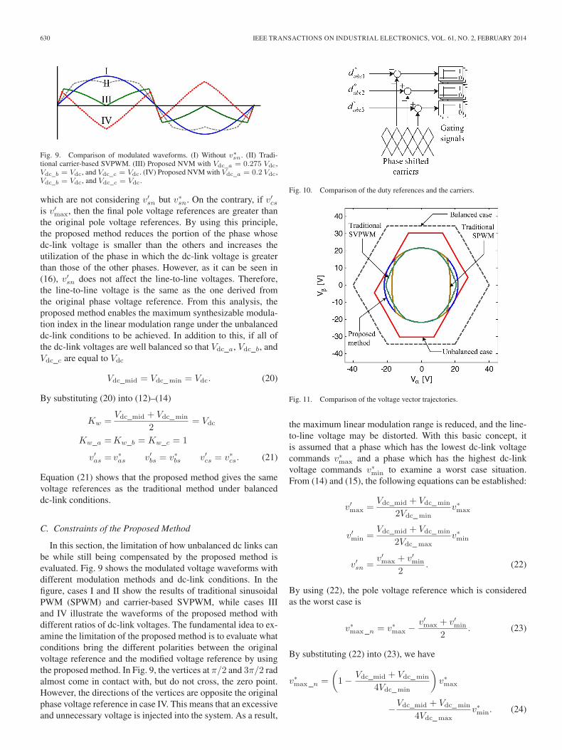
Fig. 9. Comparison of modulated waveforms. (I) Without v∗sn. (II) Tradi-tional carrier-based SVPWM. (III) Proposed NVM with Vdc_a = 0.275 Vdc,Vdc_b = Vdc, and Vdc_c = Vdc. (IV) Proposed NVM with Vdc_a = 0.2 Vdc,Vdc_b = Vdc, and Vdc_c = Vdc.
which are not considering v′sn but v∗sn. On the contrary, if v′csis v′max, then the final pole voltage references are greater thanthe original pole voltage references. By using this principle,the proposed method reduces the portion of the phase whosedc-link voltage is smaller than the others and increases theutilization of the phase in which the dc-link voltage is greaterthan those of the other phases. However, as it can be seen in(16), v′sn does not affect the line-to-line voltages. Therefore,the line-to-line voltage is the same as the one derived fromthe original phase voltage reference. From this analysis, theproposed method enables the maximum synthesizable modula-tion index in the linear modulation range under the unbalanceddc-link conditions to be achieved. In addition to this, if all ofthe dc-link voltages are well balanced so that Vdc_a, Vdc_b, andVdc_c are equal to Vdc
Vdc_mid = Vdc_min = Vdc. (20)
By substituting (20) into (12)–(14)
Kw =Vdc_mid + Vdc_min
2= Vdc
Kw_a =Kw_b = Kw_c = 1
v′as = v∗as v′bs = v∗bs v′cs = v∗cs. (21)
Equation (21) shows that the proposed method gives the samevoltage references as the traditional method under balanceddc-link conditions.
C. Constraints of the Proposed Method
In this section, the limitation of how unbalanced dc links canbe while still being compensated by the proposed method isevaluated. Fig. 9 shows the modulated voltage waveforms withdifferent modulation methods and dc-link conditions. In thefigure, cases I and II show the results of traditional sinusoidalPWM (SPWM) and carrier-based SVPWM, while cases IIIand IV illustrate the waveforms of the proposed method withdifferent ratios of dc-link voltages. The fundamental idea to ex-amine the limitation of the proposed method is to evaluate whatconditions bring the different polarities between the originalvoltage reference and the modified voltage reference by usingthe proposed method. In Fig. 9, the vertices at π/2 and 3π/2 radalmost come in contact with, but do not cross, the zero point.However, the directions of the vertices are opposite the originalphase voltage reference in case IV. This means that an excessiveand unnecessary voltage is injected into the system. As a result,
Fig. 10. Comparison of the duty references and the carriers.
Fig. 11. Comparison of the voltage vector trajectories.
the maximum linear modulation range is reduced, and the line-to-line voltage may be distorted. With this basic concept, itis assumed that a phase which has the lowest dc-link voltagecommands v∗max and a phase which has the highest dc-linkvoltage commands v∗min to examine a worst case situation.From (14) and (15), the following equations can be established:
v′max =Vdc_mid + Vdc_min
2Vdc_minv∗max
v′min =Vdc_mid + Vdc_min
2Vdc_maxv∗min
v′sn =v′max + v′min
2. (22)
By using (22), the pole voltage reference which is consideredas the worst case is
v∗max_n = v∗max −v′max + v′min
2. (23)
By substituting (22) into (23), we have
v∗max_n =
(1− Vdc_mid + Vdc_min
4Vdc_min
)v∗max
−Vdc_mid + Vdc_min
4Vdc_maxv∗min. (24)

CHO et al.: CARRIER-BASED NVM STRATEGY FOR MLCIs UNDER UNBALANCED DC SOURCES 631
Fig. 12. Simulation result of traditional SPWM, traditional SVPWM, and the proposed method.
Unless all three-phase voltage references are not zero simulta-neously, near a positive peak of the original voltage reference,the sufficient condition which guarantees the same polaritybetween v∗max and v∗min is established as follows:
v∗max_n > 0 v∗max > 0 v∗min < 0. (25)
By substituting (24) into the first condition in (25), the follow-ing condition can be written:
k1v∗max >k2v
∗min k1 = 1− Vdc_mid + Vdc_min
4Vdc_min
k2 =Vdc_mid + Vdc_min
4Vdc_max. (26)
Here, it is obvious that k2 is always positive. Therefore, as longas k1 is positive, the condition (26) is always satisfied, and k1can be rearranged as follows:
k1 =
(3Vdc_min − Vdc_mid
4Vdc_min
). (27)
Equation (28) is then directly obtained from (27) to ensure thatk1 will always be positive
Vdc_min >1
3Vdc_mid. (28)
Note that (28) is a sufficient condition to meet the conditions in(25) so that the proposed method can be applied. However, evenif (28) is not satisfied so that k1 is negative, there still is a chanceto apply the proposed method. To deal with this situation, let usconsider the relationship between v∗max and v∗min as follows ata positive peak point:
v∗max = −2v∗min. (29)
By substituting (29) into (26), we have
−2k1 > k2. (30)
Since k1 is negative in this case, the following condition isderived from (30);
|k1| <k22. (31)
If the relationship between k1 and k2 is established as in (31),even if the provision in (28) is broken, the conditions in (25)are satisfied so that the proposed method can be still effective.Let us recall Fig. 9 again here. In the figure, the values of|k1| and k2/2 for case III are evaluated as 0.1591 and 0.1593,respectively. Although the difference between the two valuesis very small, (31) is still true with these values. For case IV,

632 IEEE TRANSACTIONS ON INDUSTRIAL ELECTRONICS, VOL. 61, NO. 2, FEBRUARY 2014
Fig. 13. Photograph of the experimental setup.
the values of |k1| and k2/2 are calculated as 0.5 and 0.3,respectively. In contrast to case III, (31) is no longer satisfied,and the directions of the vertices are opposite, as explainedpreviously. From the analysis in this section, both the methodsin (28) and (31) are successfully able to judge the availability ofthe proposed method. In terms of accuracy, the latter may givebetter results. However, in practice, the former may be usefulto judge the operation of the proposed method because it isalready dealing with an extremely worst case on its own andthe calculation in real time is much simpler than (31).
D. Duty Calculation
In Fig. 8, the final voltage references are entered to the dutyreference calculation block. In this block, the duty references ofeach H-bridge module are calculated as follows:
d∗a1 = d∗a2 = · · · · · = d∗aN =v∗anVdc_a
d∗b1 = d∗b2 = · · · · · = d∗bN =v∗bnVdc_b
d∗c1 = d∗c2 = · · · · · = d∗cN =v∗cnVdc_c
. (32)
The calculated duty references are compared to PS carriers togenerate gating signals, as shown in Fig. 10. It should be notedthat the duty references for each H-bridge in each phase areshared in the PS modulation.
IV. SIMULATION
A simple one-by-three configuration MLCI model is built inMatlab Simulink. The three-phase RL load with R = 0.1 Ω andL = 1 mH is employed. The dc-link voltages for each phase areVdc_a = 0.5× 30 V, Vdc_b = 0.75× 30 V, and Vdc_c = 30 V.From (7), the maximum synthesizable phase voltage in linear is
Vph_max =0.75× 30 + 0.5× 30√
3= 21.65 V. (33)
Fig. 14. Experimental results of the traditional SVPWM and the proposedNVM strategies (50 ms/div).
Fig. 15. Phase-a voltage reference and the line-to-line voltage betweenphases a and b (20 ms/div). (a) Traditional SVPWM. (b) Proposed NVM.
The voltage references are given by
v∗as =Vph_max sin(100πt)
v∗bs =Vph_max sin(100πt− 2π/3)
v∗cs =Vph_max sin(100πt+ 2π/3). (34)
Equation (34) is applied to the modulators of the inverter inopen loop. Fig. 11 compares the voltage vector spaces andthe voltage trajectories in the α−β-axes of traditional SPWM,traditional SVPWM, and the proposed NVM method under thegiven simulation condition. Compared to the balanced dc-linkcase, the area of the voltage vector space is reduced underthe unbalanced dc-link condition. In the figure, the traditionalSPWM shows the worst voltage distortion and the minimumvoltage vector space. The traditional SVPWM gives more areathan SPWM, but still, the voltage distortion is not avoidable.The proposed method shows no distortion on the output voltage
CHO et al.: CARRIER-BASED NVM STRATEGY FOR MLCIs UNDER UNBALANCED DC SOURCES 633
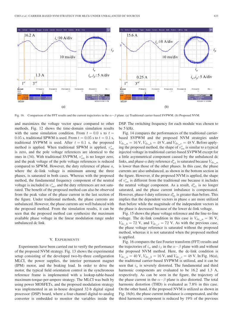
Fig. 16. Comparison of the FFT results and the current trajectories in the α−β plane. (a) Traditional carrier-based SVPWM. (b) Proposed NVM.
and maximizes the voltage vector space compared to othermethods. Fig. 12 shows the time-domain simulation resultswith the same simulation condition. From t = 0.0 s to t =0.05 s, traditional SPWM is used. From t = 0.05 s to t = 0.1 s,traditional SVPWM is used. After t = 0.1 s, the proposedmethod is applied. When traditional SPWM is applied, v∗snis zero, and the pole voltage references are identical to theones in (34). With traditional SVPWM, v∗sn is no longer zero,and the peak voltage of the pole voltage references is reducedcompared to SPWM. However, the duty reference of phase a,where the dc-link voltage is minimum among the threephases, is saturated in both cases. Whereas with the proposedmethod, the fundamental frequency component of the neutralvoltage is included in v∗sn, and the duty references are not satu-rated. The benefit of the proposed method can also be observedfrom the peak value of the phase current in the last section ofthe figure. Under traditional methods, the phase currents areunbalanced. However, the phase currents are well balanced withthe proposed method. From the simulation results, it can beseen that the proposed method can synthesize the maximumavailable phase voltage in the linear modulation range underunbalanced dc link.
V. EXPERIMENTS
Experiments have been carried out to verify the performanceof the proposed NVM strategy. Fig. 13 shows the experimentalsetup consisting of the developed two-by-three configurationMLCI, the power supplies, the interior permanent magnet(IPM) motor, and the braking load. In order to drive themotor, the typical field orientation control in the synchronousreference frame is implemented with a lookup-table-basedmaximum-torque-per-ampere strategy. The MLCI was built byusing power MOSFETs, and the proposed modulation strategywas implemented in an in-house designed 32-b digital signalprocessor (DSP) board, where a four-channel digital-to-analogconverter is embedded to monitor the variables inside the
DSP. The switching frequency for each module was chosen tobe 5 kHz.
Fig. 14 compares the performances of the traditional carrier-based SVPWM and the proposed NVM strategies underVdc_a = 16 V, Vdc_b = 48 V, and Vdc_c = 48 V. Before apply-ing the proposed method, the shape of v∗sn is similar to a typicalinjected voltage in traditional carrier-based SVPWM except fora little asymmetrical component caused by the unbalanced dclinks, and phase-a duty reference d∗a1 is saturated because Vdc_ais lower than those of the other phases. In this case, the phasecurrents are also unbalanced, as shown in the bottom section inthe figure. However, if the proposed NVM is applied, the shapeof v∗sn is different from the traditional one because it includesthe neutral voltage component. As a result, d∗a1 is no longersaturated, and the phase current imbalance is compensated.However, phase-b duty reference d∗b1 is greater than before. Thisimplies that the dependent vectors in phase a are more utilizedthan before while the magnitude of the independent vectors inthe phase is decreased because of the lower dc-link voltage.
Fig. 15 shows the phase voltage reference and the line-to-linevoltage. The dc-link condition in this case is Vdc_a = 36 V,Vdc_b = 72 V, and Vdc_c = 72 V. As with the previous case,the phase voltage reference is saturated without the proposedmethod, whereas it is not saturated when the proposed methodis applied.
Fig. 16 compares the fast Fourier transform (FFT) results andthe trajectories of iα and iβ in the α−β plane with and withoutthe proposed NVM method. Here, the dc-link condition isVdc_a = 40 V, Vdc_b = 16 V, and Vdc_c = 48 V. In Fig. 16(a),the traditional carrier-based SVPWM is utilized, and it can beseen that ia is severely distorted. The fundamental and thirdharmonic components are evaluated to be 16.2 and 1.3 A,respectively. As can be seen in the figure, the trajectory ofthe phase current in the α−β plane is also distorted. The totalharmonic distortion (THD) is evaluated as 7.8% in this case.On the other hand, if the proposed NVM is utilized as shown inFig. 16(b), the phase current imbalance is compensated, and thethird harmonic component is reduced by 19% of the previous

634 IEEE TRANSACTIONS ON INDUSTRIAL ELECTRONICS, VOL. 61, NO. 2, FEBRUARY 2014
Fig. 17. d- and q-axis current responses (200 ms/div).
Fig. 18. Phase voltage references and ia (100 ms/div).
condition. The shape of the current trajectory in the α−β planeis also improved, and the measured THD is about 4.13%.
Fig. 17 compares the d- and q-axis currents id and iq ofthe IPM motor without and with the proposed method underthe same dc-link condition with the previous test. Without theproposed method, both id and iq have ripple components be-cause the output current is unbalanced. If the proposed NVMis applied, the phase current imbalance is compensated, and theripple components are eliminated. The magnitude of the currentripple in iq is reduced by 50%.
In fact, balancing of the output voltage can be also verifiedfrom the phase voltage references, as shown in Fig. 18. Beforeapplying the proposed method, the phase voltage references arehighly unbalanced because of the unbalanced phase currents.However, once the proposed NVM is utilized, the phase voltagereferences are balanced, and the phase current becomes moresinusoidal.
In Fig. 19, the injected voltages with the traditional andproposed methods are represented as v∗sn_svm and v∗sn_nvm,respectively. Here, both the traditional and proposed methods
Fig. 19. Comparison of the injected voltages (100 ms/div).
are implemented simultaneously. In order to extract the injectedneutral voltage component v∗nv from v∗sn_nvm, v∗sn_svm is sub-tracted from v∗sn_nvm. As can be seen in the figure, with theproposed method, the neutral voltage v∗nv whose frequency isidentical to the fundamental operating frequency is includedin v∗sn_nvm to balance the output line-to-line voltages and toincrease the linear modulation capability. On the other hand,the shape of the third harmonic component is more equalizedafter the proposed NVM is applied because the phase voltageand current imbalances are compensated.
In sum, these experimental results show that the proposedNVM method compensates the voltage and current imbalancesunder unbalanced dc-link conditions in the MLCI as well asmaximizes the linear modulation range.
VI. CONCLUSION
The NVM technique for MLCIs under unbalanced dc-linkconditions has been proposed in this paper. In order to analyzethe maximum synthesizable voltage of MLCIs, the voltagevector space has been analyzed using the switching function.From the analysis, the maximum linear modulation range wasderived. The proposed NVM technique is applied to achievethe maximum modulation index in the linear modulation rangeunder an unbalanced dc-link condition as well as to balance theoutput phase voltages. Compared to the previous methods,the proposed technique is easily implemented and improvesthe output voltage quality under unbalanced dc-link conditions.Both simulations and experimental results based on the IPMmotor drive application verify the effectiveness of the proposedmethod.
REFERENCES
[1] J. Rodriguez, J.-S. Lai, and F. Z. Peng, “Multilevel inverters: A surveyof topologies, controls, and applications,” IEEE Trans. Ind. Electron.,vol. 49, no. 4, pp. 724–738, Aug. 2002.
[2] H. Abu-Rub, J. Holtz, J. Rodriguez, and G. Baoming, “Medium-voltagemultilevel converters—State of the art, challenges, and requirements in in-dustrial applications,” IEEE Trans. Ind. Electron., vol. 57, no. 8, pp. 2581–2596, Aug. 2010.

CHO et al.: CARRIER-BASED NVM STRATEGY FOR MLCIs UNDER UNBALANCED DC SOURCES 635
[3] J.-S. Lai and F. Z. Peng, “Multilevel converters—A new breed ofpower converters,” IEEE Trans. Ind. Appl., vol. 32, no. 3, pp. 509–517,May/Jun. 1996.
[4] M. Malinowski, K. Gopakumar, J. Rodriguez, and M. A. Perez, “A surveyon cascaded multilevel inverters,” IEEE Trans. Ind. Electron., vol. 57,no. 7, pp. 2197–2206, Jul. 2010.
[5] J. Rodriguez, L. G. Franquelo, S. Kouro, J. I. León, R. C. Portillo,M. A. M. Prats, and M. A. Perez, “Multilevel converters: An enablingtechnology for high-power applications,” Proc. IEEE, vol. 97, no. 11,pp. 1786–1817, Nov. 2009.
[6] G. Bergna, E. Berne, P. Egrot, P. Lefranc, A. Arzande, J.-C. Vannier,and M. Molinas, “An energy-based controller for HVDC modular mul-tilevel converter in decoupled double synchronous reference frame forvoltage oscillation reduction,” IEEE Trans. Ind. Electron., vol. 60, no. 6,pp. 2360–2371, Jun. 2013.
[7] Z. Shu, N. Ding, J. Chen, H. Zhu, and X. He, “Multilevel SVPWM withDC-link capacitor voltage balancing control for diode-clamped multilevelconverter based STATCOM,” IEEE Trans. Ind. Electron., vol. 60, no. 5,pp. 1884–1896, May 2013.
[8] J. Chavarria, D. Biel, F. Guinjoan, C. Meza, and J. J. Negroni, “Energy-balance control of PV cascaded multilevel grid-connected inverters un-der level-shifted and phase-shifted PWMs,” IEEE Trans. Ind. Electron.,vol. 60, no. 1, pp. 98–111, Jan. 2013.
[9] G. Buticchi, E. Lorenzani, and G. Franceschini, “A five-level single-phasegrid-connected converter for renewable distributed systems,” IEEE Trans.Ind. Electron., vol. 60, no. 3, pp. 906–918, Mar. 2013.
[10] J. A. Munoz, J. R R. Espinoza, C. R. Baier, L. L. Morán, E. E. Espinosa,P. E. Melín, and D. G. Sbárbaro, “Design of a discrete-time linear controlstrategy for a multicell UPQC,” IEEE Trans. Ind. Electron., vol. 59,no. 10, pp. 3797–3807, Oct. 2012.
[11] J. Napoles, J. I. Leon, R. Portillo, L. G. Franquelo, and M. A. Aguirre,“Selective harmonic mitigation technique for high-power converters,”IEEE Trans. Ind. Electron., vol. 57, no. 7, pp. 2315–2323, Jul. 2010.
[12] L. G. Franquelo, J. Napoles, R. C. Portillo Guisado, J. I. Leon, andM. A. Aguirre, “A flexible selective harmonic mitigation technique tomeet grid codes in three-level PWM converters,” IEEE Trans. Ind. Elec-tron., vol. 54, no. 6, pp. 3022–3029, Dec. 2007.
[13] S. Kouro, M. Malinowski, K. Gopakumar, J. Pou, L. G. Franquelo,and B. Wu, “Recent advances and industrial applications of multilevelconverters,” IEEE Trans. Ind. Electron., vol. 57, no. 8, pp. 2553–2580,Aug. 2010.
[14] A. M. Massoud, S. Ahmed, P. N. Enjeti, and B. W. Williams, “Evaluationof a multilevel cascaded-type dynamic voltage restorer employing dis-continuous space vector modulation,” IEEE Trans. Ind. Electron., vol. 57,no. 7, pp. 2398–2410, Jul. 2010.
[15] M. Hagiwara, K. Nishimura, and H. Akagi, “A medium-voltage motordrive with a modular multilevel PWM inverter,” IEEE Trans. Power Elec-tron., vol. 25, no. 7, pp. 1786–1799, Jul. 2010.
[16] J. Rodriguez, S. Bernet, B. Wu, J. O. Pontt, and S. Kouro, “Multi-level voltage-source-converter topologies for industrial medium-voltagedrives,” IEEE Trans. Ind. Electron., vol. 54, no. 6, pp. 2930–2945,Dec. 2007.
[17] L. Maharjan, S. Inoue, and H. Akagi, “A transformerless energy stor-age system based on a cascade multilevel PWM converter with starconfiguration,” IEEE Trans. Ind. Appl., vol. 44, no. 5, pp. 1621–1630,Sep./Oct. 2008.
[18] W. Song and A. Q. Huang, “Fault-tolerant design and control strategy forcascaded H-bridge multilevel converter-based STATCOM,” IEEE Trans.Ind. Electron., vol. 57, no. 8, pp. 2700–2708, Aug. 2010.
[19] E. Villanueva, P. Correa, J. Rodriguez, and M. Pacas, “Control of a single-phase cascaded H-bridge multilevel inverter for grid-connected photo-voltaic systems,” IEEE Trans. Ind. Electron., vol. 56, no. 11, pp. 4399–4406, Nov. 2009.
[20] C. Cecati, F. Ciancetta, and P. Siano, “A multilevel inverter for photo-voltaic systems with fuzzy logic control,” IEEE Trans. Ind. Electron.,vol. 57, no. 12, pp. 4115–4125, Dec. 2010.
[21] C. H. Ng, M. A. Parker, R. Li, P. J. Tavner, J. R. Bumby, and E. Spooner,“A multilevel modular converter for a large, light weight wind turbinegenerator,” IEEE Trans. Power Electron., vol. 23, no. 3, pp. 1062–1074,May 2008.
[22] F. Khoucha, S. M. Lagoun, K. Marouani, A. Kheloui, and M. E. H. Ben-bouzid, “Hybrid cascaded H-bridge multilevel-inverter induction-motor-drive direct torque control for automotive applications,” IEEE Trans. Ind.Electron., vol. 57, no. 3, pp. 892–899, Mar. 2010.
[23] L. M. Tolbert, F. Z. Peng, and T. G. Habetler, “Multilevel converters forlarge electric drives,” IEEE Trans. Ind. Appl., vol. 35, no. 1, pp. 36–44,Jan./Feb. 1999.
[24] Z. Du, B. Ozpineci, L. M. Tolbert, and J. N. Chiasson, “DC–AC cascadedH-bridge multilevel boost inverter with no inductors for electric/hybridelectric vehicle applications,” IEEE Trans. Ind. Appl., vol. 45, no. 3,pp. 963–970, May/Jun. 2009.
[25] A. K. Gupta and A. M. Khambadkone, “A general space vector PWMalgorithm for multilevel inverters, including operation in overmodula-tion range,” IEEE Trans. Power Electron., vol. 22, no. 2, pp. 517–526,Mar. 2007.
[26] A. K. Gupta and A. M. Khambadkone, “A space vector modulationscheme to reduce common mode voltage for cascaded multilevel in-verters,” IEEE Trans. Power Electron., vol. 22, no. 5, pp. 1672–1681,Sep. 2007.
[27] R. Rabinovici, D. Baimel, J. Tomasik, and A. Zuckerberger, “Seriesspace vector modulation for multi-level cascaded H-bridge inverters,” IETPower Electron., vol. 3, no. 6, pp. 843–857, Nov. 2010.
[28] Z. Cheng and B. Wu, “A novel switching sequence design for five-levelNPC/H-bridge inverters with improved output voltage spectrum and mini-mized device switching frequency,” IEEE Trans. Power Electron., vol. 22,no. 6, pp. 2138–2145, Nov. 2007.
[29] B. P. McGrath, D. G. Homes, and T. Lipo, “Optimized space vectorswitching sequences for multilevel inverters,” IEEE Trans. Power Elec-tron., vol. 18, no. 6, pp. 1293–1301, Nov. 2003.
[30] D.-W. Kang, Y.-H. Lee, B.-S. S. Suh, C.-H. H. Choi, and D.-S. S. Hyun,“An improved carrier-based SVPWM method using leg voltage redundan-cies in generalized cascaded multilevel inverter topology,” IEEE Trans.Power Electron., vol. 18, no. 1, pp. 180–187, Jan. 2003.
[31] W. Yao, H. Hu, and Z. Lu, “Comparisons of space-vector modulationand carrier-based modulation of multilevel inverter,” IEEE Trans. PowerElectron., vol. 23, no. 1, pp. 45–51, Jan. 2008.
[32] M. Ma, L. Hu, A. Chen, and X. He, “Reconfiguration of carrier-basedmodulation strategy for fault tolerant multilevel inverters,” IEEE Trans.Power Electron., vol. 22, no. 5, pp. 2050–2060, Sep. 2007.
[33] Q. Song and W. Liu, “Control of a cascade STATCOM with star configura-tion under unbalanced conditions,” IEEE Trans. Power Electron., vol. 24,no. 1, pp. 45–58, Jan. 2009.
[34] P. Lezana and G. Ortiz, “Extended operation of cascade multicell con-verters under fault condition,” IEEE Trans. Ind. Electron., vol. 56, no. 7,pp. 2697–2703, Jul. 2009.
[35] L. Maharjan, T. Yamagishi, H. Akagi, and J. Asakura, “Fault-tolerant op-eration of a battery-energy-storage system based on a multilevel cascadePWM converter with star configuration,” IEEE Trans. Power Electron.,vol. 25, no. 9, pp. 2386–2396, Sep. 2010.
[36] V. Naumanen, J. Luukko, P. Silventoinen, J. Pyrhonen, H. Saren, andK. Rauma, “Compensation of DC link voltage variation of a multilevelseries-connected H-bridge inverter,” IET Power Electron., vol. 3, no. 5,pp. 793–803, Sep. 2010.
[37] J. Rodriguez, P. W. Hammond, J. Pontt, R. Musalem, P. Lezana, andM. J. Escobar, “Operation of a medium-voltage drive under faulty con-ditions,” IEEE Trans. Ind. Electron., vol. 52, no. 4, pp. 1080–1085,Aug. 2005.
[38] Y.-M. Park, H.-S. Ryu, H.-W. Lee, M.-G. Jung, and S.-H. Lee, “Designof a cascaded h-bridge multilevel inverter based on power electronicsbuilding blocks and control for high performance,” J. Power Electron.,vol. 10, no. 3, pp. 262–269, May 2010.
[39] J. I. Leon, O. Lopez, L. G. Franquelo, J. Doval-Gandoy, S. Vazquez,J. Alvarez, and F. D. Freijedo, “Multilevel multiphase feedforward space-vector modulation technique,” IEEE Trans. Ind. Electron., vol. 57, no. 6,pp. 2066–2075, Jun. 2010.
[40] R. Gupta, A. Ghosh, and A. Joshi, “Switching characterization of cas-caded multilevel-inverter-controlled systems,” IEEE Trans. Ind. Electron.,vol. 55, no. 3, pp. 1047–1058, Mar. 2008.
[41] Y. Li and B. Wu, “A novel DC voltage detection technique in the CHBinverter-based STATCOM,” IEEE Trans. Power Del., vol. 23, no. 3,pp. 1613–1619, Jul. 2008.
[42] R. Naderi and A. Rahmati, “Phase-shifted carrier PWM technique forgeneral cascaded inverters,” IEEE Trans. Power Electron., vol. 23, no. 3,pp. 1257–1269, May 2008.
[43] D.-W. Chung, J.-S. Kim, and S.-K. Sul, “Unified voltage modulationtechnique for real-time three-phase power conversion,” IEEE Trans. Ind.Appl., vol. 34, no. 2, pp. 374–380, Mar./Apr. 1998.
[44] F. Wang, “Sine-triangle versus space-vector modulation for three-levelPWM voltage-source inverters,” IEEE Trans. Ind. Appl., vol. 38, no. 2,pp. 500–506, Mar./Apr. 2002.
[45] F. Carnielutti, H. Pinheiro, and C. Rech, “Generalized carrier-based mod-ulation strategy for cascaded multilevel converters operating under faultconditions,” IEEE Trans. Ind. Electron., vol. 59, no. 2, pp. 679–689,Feb. 2012.

636 IEEE TRANSACTIONS ON INDUSTRIAL ELECTRONICS, VOL. 61, NO. 2, FEBRUARY 2014
Younghoon Cho (S’10–M’13) was born in Seoul,Korea, in 1980. He received the B.S. degree in elec-trical engineering from Konkuk University, Seoul, in2002, the M.S. degree in electrical engineering fromSeoul National University, Seoul, in 2004, and thePh.D. degree from Virginia Polytechnic Institute andState University, Blacksburg, VA, USA, in 2012.
From 2004 to 2009, he was an Assistant ResearchEngineer with the Hyundai MOBIS R&D Center,Yongin, Korea. Since 2013, he has been with theDepartment of Electrical Engineering, Konkuk Uni-
versity, Seoul. His current research interests include digital control techniquesfor power electronic converters in vehicle and grid applications, multilevelconverters, and high-performance motor drives.
Thomas LaBella (S’07) received the B.S. andM.S. degrees in electrical engineering from VirginiaPolytechnic Institute and State University (VirginiaTech), Blacksburg, VA, USA, in 2009 and 2011,respectively, where he is currently working towardthe Ph.D. degree in power electronics.
Since 2009, he has been a Graduate ResearchAssistant with the Future Energy Electronics Center,Virginia Tech. His research interests include powerconditioning system design and control for renew-able energy applications as well as sensorless control
of permanent-magnet machines for high-performance ac drives.
Jih-Sheng (Jason) Lai (S’85–M’89–SM’93–F’07)received the M.S. and Ph.D. degrees in electri-cal engineering from the University of Tennessee,Knoxville, TN, USA, in 1985 and 1989, respectively.
From 1980 to 1983, he was the Head of the Elec-trical Engineering Department, Ming-Chi Instituteof Technology, New Taipei City, Taiwan, where heinitiated a power electronics program and receiveda grant from his college and a fellowship from theNational Science Council to study abroad. In 1986,he became a staff member at the University of Ten-
nessee, where he taught control system and energy conversion courses. In 1989,he joined the Power Electronics Applications Center, Electric Power ResearchInstitute (EPRI), where he managed EPRI-sponsored power electronics re-search projects. Beggining in 1993, he worked with the Oak Ridge NationalLaboratory as the Power Electronics Lead Scientist, where he initiated a high-power electronics program and developed several novel high-power converters,including multilevel converters and soft-switching inverters. His work broughthim several distinctive awards, including a Technical Achievement Award atLockheed Martin Award Night, three IEEE Industry Applications Society Con-ference Paper Awards, and Best Paper Awards from IECON’97, IPEC’05, andPCC’07. In 1996, he joined Virginia Polytechnic Institute and State University,Blacksburg, VA, USA, where he is currently the James S. Tucker Professor andthe Director of the Future Energy Electronics Center. His student teams havewon three awards from future energy challenge competitions and the first placeaward from the Texas Instruments Engibous Prize Analog Design Competition.He has published more than 265 technical papers and two books and is theholder of 20 U.S. patents. His main research areas are in high-efficiency powerelectronics conversions for high power and energy applications.
Dr. Lai was the Chair of the 2000 IEEE Workshop on Computers inPower Electronics, the 2001 IEEE/U.S. Department of Energy Future EnergyChallenge, and the 2005 IEEE Applied Power Electronics Conference andExposition.
Matthew K. Senesky (S’03–M’05) received theA.B. and B.E. degrees from Dartmouth College,Hanover, NH, USA, and the M.S. and Ph.D. de-grees in electrical engineering from the Universityof California, Berkeley, CA, USA. His academicresearch included topics in flywheel energy storageand microscale power generation.
Since graduating in 2005, he has held positions atArtificial Muscle, Tesla Motors, and National Semi-conductor. He is currently with Texas InstrumentsIncorporated, Santa Clara, CA, USA, where he per-
forms R&D in power electronics for renewable energy, energy storage, andelectric vehicle applications.