a class-c type wideband current-reused vco with...
TRANSCRIPT
JOURNAL OF SEMICONDUCTOR TECHNOLOGY AND SCIENCE, VOL.15, NO.5, OCTOBER, 2015 ISSN(Print) 1598-1657 http://dx.doi.org/10.5573/JSTS.2015.15.5.470 ISSN(Online) 2233-4866
Manuscript received Apr. 16, 2015; accepted Jul. 6, 2015 College of Information and Communication Engineering, Sungkyunkwan University E-mail : [email protected]�
A Class-C Type Wideband Current-Reused VCO With Two-Step Automatic Amplitude Calibration Loop
Jin-Wook Choi, Seung-Won Choi, InSeong Kim, DongSoo Lee, HyungGu Park,
YoungGun Pu, and Kang-Yoon Lee
Abstract—This paper presents a wideband Current-Reused Voltage Controlled Oscillator (VCO) with 2-Step Automatic Amplitude Calibration (AAC). Tuning range of the proposed VCO is from 1.95 GHz to 3.15 GHz. The mismatch of differential voltage is within 0.6 %. At 2.423 GHz, the phase noise is -116.3 dBc/Hz at the 1 MHz offset frequency with the current consumption of 2.6 mA. The VCO is implemented 0.13 mm CMOS technology. The layout size is 720 × 580 mm2. Index Terms—Current-reused VCO, Class-C type, AAC (Auto Amplitude Calibration)
I. INTRODUCTION
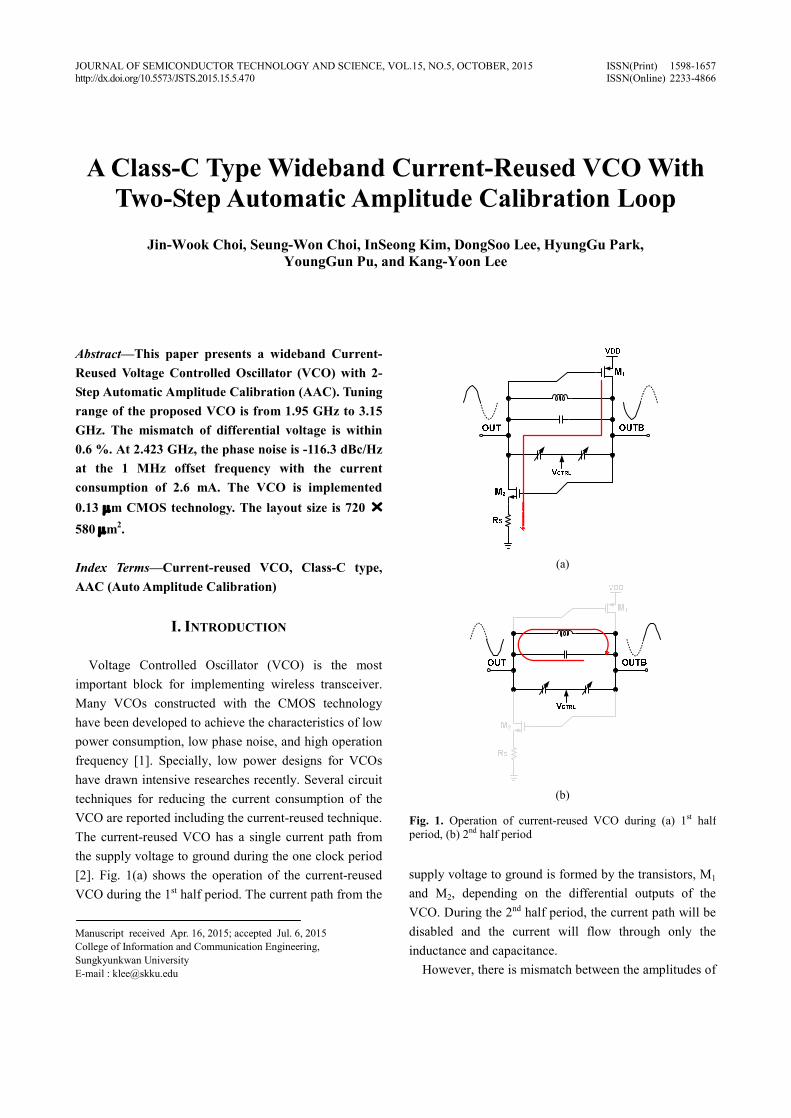
Voltage Controlled Oscillator (VCO) is the most important block for implementing wireless transceiver. Many VCOs constructed with the CMOS technology have been developed to achieve the characteristics of low power consumption, low phase noise, and high operation frequency [1]. Specially, low power designs for VCOs have drawn intensive researches recently. Several circuit techniques for reducing the current consumption of the VCO are reported including the current-reused technique. The current-reused VCO has a single current path from the supply voltage to ground during the one clock period [2]. Fig. 1(a) shows the operation of the current-reused VCO during the 1st half period. The current path from the
supply voltage to ground is formed by the transistors, M1 and M2, depending on the differential outputs of the VCO. During the 2nd half period, the current path will be disabled and the current will flow through only the inductance and capacitance.
However, there is mismatch between the amplitudes of
(a)
(b)
Fig. 1. Operation of current-reused VCO during (a) 1st half period, (b) 2nd half period

JOURNAL OF SEMICONDUCTOR TECHNOLOGY AND SCIENCE, VOL.15, NO.5, OCTOBER, 2015 471
differential outputs due to the asymmetric structure and operation. The overall system performance can be degraded due to the noise and distortion of the differential outputs. In this paper, the class-C type VCO [2] with 2-step automatic amplitude calibration (AAC) is proposed to compensate for the structural unbalance in addition to the unbalances due to the process variations.
II. PROPOSED CURRENT-REUSED VCO
The most important issue of Current-reused VCO is voltage imbalance at outputs. Because the unbalanced outputs of the VCO will result in the imbalance of In-Phase and Quadrature-Phase Local Oscillator (LO) signals degrading the Error Vector Magnitude (EVM) performance of the receiver. To solve this problem, researchers have been studied how to reduce the voltage mismatch. The methods are forcing proper negative-Gm bias voltage for maximizing voltage swing or inserting the resistor at the source of NMOS to minimize voltage mismatch [4]. We propose 2-step AAC method to reduce the voltage mismatch and dynamic current. Fig. 2 shows proposed current-reused VCO with 2-Step AAC Loop. As shown in Fig. 2, the 2-step AAC loop consists of peak detector, comparator and Control logic. First, at 1st AAC
loop, the peak detector senses the peak level of voltage outputs.
Fig. 3 and 4 show timing diagram and flow chart of 2-step AAC loop, respectively. After output of peak detector is compared with reference voltage (VREF1) which is generated by a bias block. If the output level of peak detector is bigger than the reference voltage, the gate bias voltage control bits, BIAS_CONT1<2:0> and BIAS_CONT2<1:0>, are adjusted from “000” to “111 until the outputs of the Peak Detectors are less than the reference levels, VREF1 and VREF2, respectively. Result from this process, VBIASN or VBIASP which is negative-gm bias voltage can be changed as shown in Fig. 3. When the output of peak detector is smaller than the reference voltage, 1st AAC loop end and 2nd AAC loop start. Overall operation of 2nd AAC loop is similar with 1st AAC loop. At the 2nd AAC loop, RES_CONT<9:0> controls the resistor value instead of negative-gm bias voltage in 1st AAC loop. In the second stage, firstly the peak detector output is compared with the reference voltage (VREF2) in the comparator. Depending on
Fig. 2. Proposed current-reused VCO with 2-step AAC loop
Fig. 3. Timing diagram of 2-step automatic amplitude calibration Loop
Fig. 4. Flow chart of 2-step automatic amplitude calibration Loop

472 JIN-WOOK CHOI et al : A CLASS-C TYPE WIDEBAND CURRENT-REUSED VCO WITH TWO-STEP AUTOMATIC AMPLITUDE …
comparator output RES_CONT<9:0> is determined. This operation continues until the output of peak detector is lower than VREF2. Through this process, resistor control bits (RES_CONT<9:0>) are changed by control logic block. According to resistor, dynamic current of VCO is controlled and the mismatch of differential outputs can be reduced.
III. EXPERIMENTAL RESULTS
Fig. 5 is the layout of proposed VCO. The size is 720 x 580 mm 2. Fig. 6 shows the operation sequence of the proposed current-reused VCO. After starting the oscillation (State2) of the VCO by a Start-up signal, (State 1), the two-step AAC calibration loop is enabled.
Fig. 7 shows the simulation results about two-step AAC loop. When the peak detector out is higher than comparator bias voltage, so BIAS_CONT1,2 <2:0> is changed from LSB. Therefore negative-Gm bias voltages (VBIASN, VBIASP) are moved separately. Because the
output of peak detector output is still lager than VREF1, the 2nd AAC loop starts to operate. Similar to 1st AAC loop, at 2nd AAC loop, RES_CONT<9:0> can control the VCO output swing by adjusting the entire dynamic current of VCO. The 2nd AAC loop operates until the output of the peak detector is smaller than VREF2.
Fig. 8(a) and (b) show the transient simulation result of VCO without the calibration loop and with two-step AAC loop. As shown in Fig. 7(a), when the two-step AAC calibration loop is disabled, the difference between differential outputs is about 50 mV. Also, they show the distorted waveforms with the phase difference of about 5% (18˚). As shown in Fig. 7(b), by operating the two-step AAC calibration loop, the difference between the
Fig. 5. The layout of proposed VCO
Fig. 6. Operation sequence of the proposed current-reused VCO
Fig. 7. Two-step AAC loop simulation results
(a)
(b)
Fig. 8. Transient simulation result of VCO (a) without calibration loop, (b) with 2-step AAC loop

JOURNAL OF SEMICONDUCTOR TECHNOLOGY AND SCIENCE, VOL.15, NO.5, OCTOBER, 2015 473
differential outputs can be reduced to approximately 1.5 mV ~ 4.5 mV around the oscillation range.
Fig. 9 shows the measured spectrum of the proposed VCO. The output power is –6.76 dBm.
Fig. 10 shows the frequency ranges of the proposed current-reused VCO. In this paper, 8-bit Capacitor bank connected to the output s of VCO is designed to have a wide range from 1.9 GHz to 3.1 GHz.
Fig. 11 shows the measured phase noise for the proposed current-reused VCO at the oscillation frequency of 2.423 GHz. The measured values for the proposed VCOs are -116 dBc/Hz at 1 MHz offset when the current consumption is 2.6 mA. The noise floor is relatively high due to the noises from the measurement environments and test board. Table 1 represents the summary of the VCO performance compared with other papers. Overall frequency tuning range is from 1.95 GHz to 3.15 GHz and mismatch between VCO outputs is within 4.5 mV (<
0.6%). Table 1 summarizes the VCO performance and comparison with other published wideband VCOs. The figure of merit including tuning range (FOMT) in Eq. (1) is used to make fair comparison.
0( ) 20log 10log1
20log10%
DCT
f PFoM L F
f mW
FTR
æ ö æ ö= D - +ç ÷ ç ÷D è øè ø
æ ö- ç ÷è ø
(1)
IV. CONCLUSIONS
The paper proposes the Class-C type Current-Reused VCO with Two-Step AAC Loop. The tuning range of the proposed VCO is from 1.95 GHz to 3.15 GHz. The mismatch of differential voltage is within 0.6 %. At 2.423 GHz, the phase noise is -116.3 dBc/Hz at the 1 MHz offset frequency with the current consumption of
Fig. 9. The output spectrum of the proposed current-reused VCO
Fig. 10. The output frequency range of proposed current-reused VCO
Fig. 11. Measured phase noise of proposed current-reused VCO
Table 1. Performance comparison with previous works
[1] [4] [5] [6] [7] This Work
Technology (mm) 0.18 0.18 0.18 0.18 0.13 0.13 Frequency (GHz) 16 3.5 2.26 1.96 0.83 2.5 Supply Voltage
(V) 1.8 1.5 1.8 1.8 1.2 1.2
Tuning Range (%) 5.6 21 8.5 56 127 47
Phase noise @ 1MHz (dBc/Hz)
-111 -122 -121.66 -118.3 -109 -116.3
Power (mW) 8.1 2.475 1.62 14.4 13 3.12 FoMT (dBc/Hz) -186.8 -195.7 -187 -190 -186 -192.3

474 JIN-WOOK CHOI et al : A CLASS-C TYPE WIDEBAND CURRENT-REUSED VCO WITH TWO-STEP AUTOMATIC AMPLITUDE …
2.6 mA. The VCO is implemented 0.13 mm CMOS technology. The layout size is 720 × 580 mm2.
ACKNOWLEDGMENTS
This research was supported by Basic Science Research Program through the National Research Foundation of Korea(NRF) funded by the Ministry of Education(NRF-2013R1A1A2010114)
REFERENCES
[1] Chin-Lung Yang, Yi-Chyun Chiang, “Low Phase-Noise and Low-Power CMOS VCO Constructed in Current-Reused Configuration”, IEEE MICROWAVE AND WIRELESS COMPONENTS LETTERS, VOL.18, NO.2, FEBRUARY 2008
[2] Jian Chen, Fredrik Jonsson, Mats Carlsson, Charlotta Hedenäs, and Li-Rong Zheng, “A Low Power, Startup Ensured and Constant Amplitude Class-C VCO in 0.18 mm CMOS”, IEEE MICROWAVE AND WIRELESS COMPONENTS LETTERS, VOL. 21, NO. 8, AUGUST 2011
[3] S-J. Yun, S-B. Shin, H-C Choi, and S-G. Lee, "A 1 mW Current-Reuse CMOS Diffential LC-VCO with Low PhaseNoise," IEEE International Solid-State Circuits Conference(ISSCC), Digest of Technical Papers, pp. 540-541, 2005.
[4] Muh-Dey Wie, Sheng-Fuh Chang, Shih-Wei Huang, “An Amplitude-Balanced Current-Reused CMOS VCO Using Spontaneous Transconductance Match Technique”, IEEE MICROWAVE AND WIRELESS COMPONENTS LETTERS, VOL. 19, NO. 6, JUNE 2009
[5] Chien-Hsuan Liu, Chia- Yo Chan, Ruey-Lue Wang, Yun-Kuin Su, “Low Power Current-reused Voltage-Controlled Oscillator with Optimum Source Damping Resistors”, IEEE Conference on Electron Devices and Solid-State Circuits, pp. 1017-1020, DECEMBER 2007
[6] Zou,W., Chen, X., Dai, K., and Zou, X.: ‘Switched-inductor VCO based on tapped vertical solenoid inductors’, Electron. Lett., 2012, 48, (9), pp. 509–511
[7] Xu, J.T., Saavedra, C.E., and Chen, G.: ‘An active inductor-based VCO with wide tuning range and
high DC-to-RF power efficiency’, IEEE Trans. Circuits Syst. II, 2011, 58, (8), pp. 462–466
JinWook Choi received his B.S. degree from the Department of Electronic and Electrical Engineering at Sejong University, Seoul, Korea, in 2014, where he is currently working toward a M.S. degree in School of Information and Communi-
cation Engineering, Sungkyunkwan University. His research interests include Sensor and CMOS RF IC.
Seung-Won Choi received his B.S. degree from the Department of Electronic Engineering at Sungkyun- kwan University, Suwon, Korea, in 2014, where he is currently working toward the Combined Ph.D. & M.S degree in School of Information and
Communication Engineering. His research interests include CMOS RF transceiver, Phase Locked Loop, Automotive Pressure Sensor.
InSeong Kim was born in Seoul, Korea. He received his B.S degree from the Department of Electronic Engineering at Konkuk University, Seoul, Korea, in 2014, and he is currently working toward the Combined Ph.D. & M.S. Course in School of
Information and Communication Engineering, Sungkyun- kwan University. His research interests include high-speed interface IC and CMOS RF transceiver.
DongSoo Lee received his B.S., and M.S. degree from the Department of Electronic Engineering at Konkuk University, Seoul, Korea, in 2012, and the electronic engineering at Sungkyunkwan University, Suwon, Korea, in 2014, respectively. He is
currently working toward a Ph.D. degree in electronic engineering at Sungkyunkwan University. His research interests are focused on CMOS RF IC and Phase Locked Loop, Silicon Oscillator, Sensor Interfaces design.
JOURNAL OF SEMICONDUCTOR TECHNOLOGY AND SCIENCE, VOL.15, NO.5, OCTOBER, 2015 475
Hyung-Gu Park received his B.S. degree from the Department of Electronic Engineering at Konkuk University, Seoul, Korea, in 2010, where he is currently working toward the Ph.D. degree in College of Information and Communication
Engineering, Sungkyunkwan University. His research interests include high-speed interface IC and CMOS RF transceiver.
YoungGun Pu received his B.S., M.S. and Ph.D. degrees from the Department of Electronic Engineering at Konkuk University, Seoul, Korea, in 2006, 2008 and 2012, respectively. His research interest is focused on CMOS fully integrated frequency
synthesizers and oscillators and on transceivers for low-power mobile communication.
Kang-Yoon Lee received the B.S., M.S. and Ph.D. degrees in the School of Electrical Engineering from Seoul National University, Seoul, Korea, in 1996, 1998, and 2003, respectively. From 2003 to 2005, he was with GCT Semiconductor Inc., San Jose,
CA, where he was a Manager of the Analog Division and worked on the design of CMOS frequency synthesizer for CDMA/PCS/PDC and single-chip CMOS RF chip sets for W-CDMA, WLAN, and PHS. From 2005 to 2011, he was with the Department of Electronics Engineering, Konkuk University as an Associate Professor. Since 2012, he has been with College of Information and Communication Engineering, Sungkyun- kwan University, where he is currently an Associate Professor. His research interests include implementation of power integrated circuits, CMOS RF transceiver, analog integrated circuits, and analog/digital mixed-mode VLSI system design.