a closer look at recent dram releases - techinsights · •...
TRANSCRIPT

A Closer Look at Recent DRAM Releases
A t 2011August 2011

DRAM M k t G thDRAM Market Growth• Smartphone and tablet markets continue to grow at
an approximate rate of 10% a year and demand for DRAM memory has matched that growth.
• Global DRAM sales volume to increase at a rate of• Global DRAM sales volume to increase at a rate of 12.3% annually through to 2020. *source: GBI Research
• Mobile DRAM shipments estimated to reach all-time phigh in 2010 of 1.87 billion units shipped *source: DRAMeXchange
2
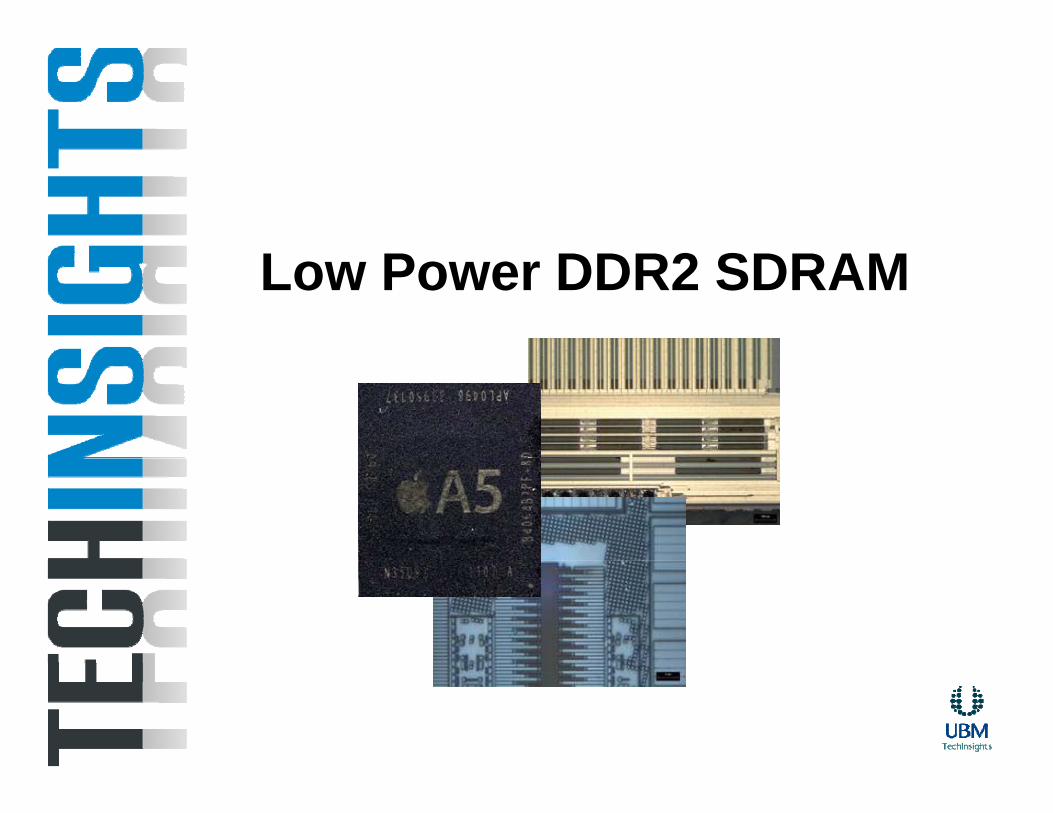
L P DDR2 SDRAMLow Power DDR2 SDRAM
El id B4064B2PF L P DDR2 SDRAMElpida B4064B2PF Low Power DDR2 SDRAM
• Found within the iPad 2 in a package-on-package with the Apple A5 processor.
• Identified by ‘B240ABB’ die marking• 2Gb LPDDR2 SDRAM manufactured at the 44nm process
node
Available reports:• Memory Detailed Structural Analysis of the Elpida B240ABB
44nm 2Gbit LPDDR2 SDRAM die found in the Apple A5 PoP• CircuitVision Analysis of the Elpida B240ABB 44nm 2Gbit y p
LPDDR2 SDRAM die found in the Apple A5 PoP• IC Review of the Elpida B4064B2PF-8D F DRAM Memory to
A5 Processor
44 I DRAM Update August 2011
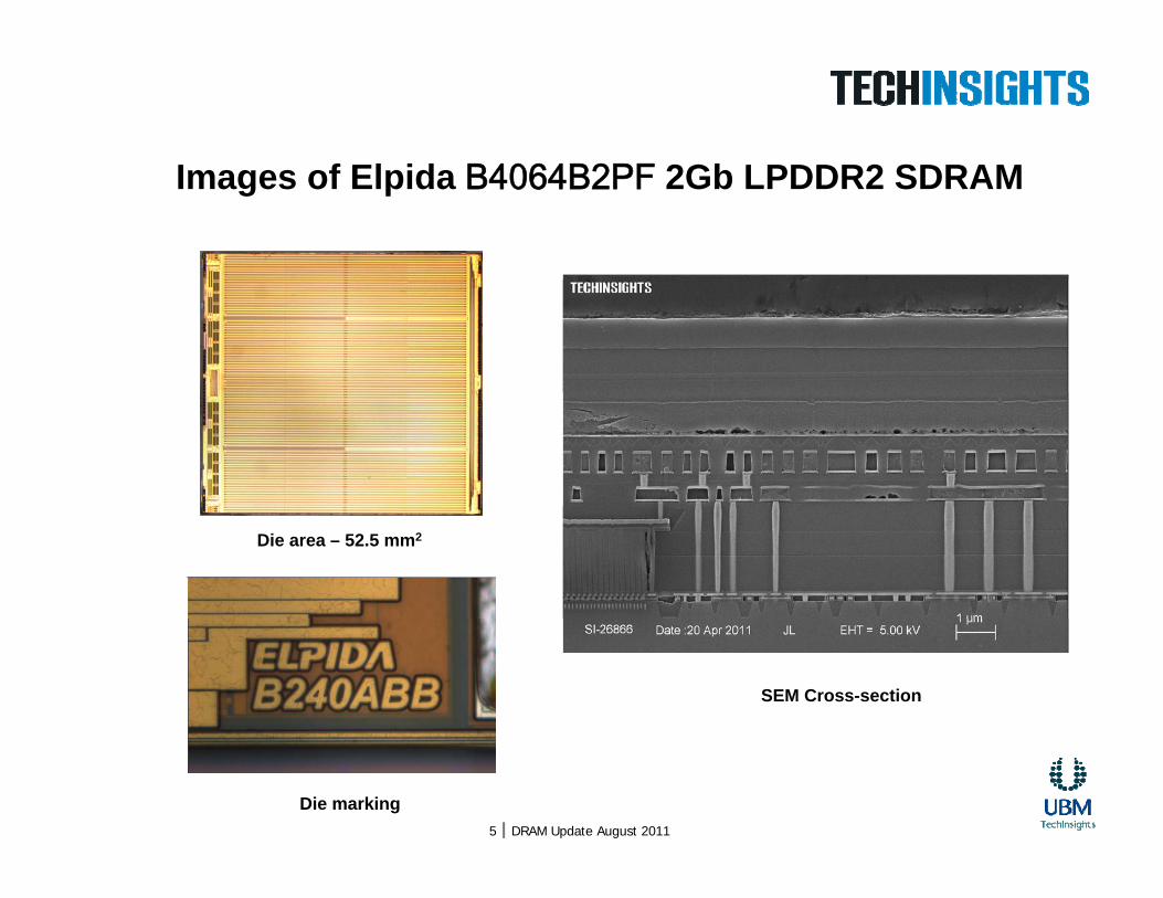
I f El id B4064B2PF 2Gb LPDDR2 SDRAMImages of Elpida B4064B2PF 2Gb LPDDR2 SDRAM
Die area – 52.5 mm2
SEM Cross-section
Die marking5 I DRAM Update August 2011
H i H5LR2G23M L P DDR2 SDRAMHynix H5LR2G23M Low Power DDR2 SDRAM
• Found within an LG handset in a package-on-package (PoP) with the Nvidea Tegra 2 processor.
• Identified by ‘H5LR2G23M’ die marking• 2Gb LPDDR2 SDRAM manufactured at the 44nm process
node
Available reports:• IC Review of the Hynix H5LR2G23M LPDDR2
SDRAMF th l i il bl t• Further analysis available on request
66 I DRAM Update August 2011
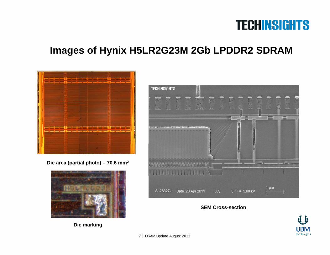
I f H i H5LR2G23M 2Gb LPDDR2 SDRAMImages of Hynix H5LR2G23M 2Gb LPDDR2 SDRAM
Die area (partial photo) – 70.6 mm2
SEM Cross-section
Die marking
SEM Cross-section
7 I DRAM Update August 2011

Micron MT42L64M32D1KL Low Power DDR2 SDRAM• Used in a package-on-package (PoP) orientation.• Identified by ‘G59A’ die marking• 2Gb LPDDR2 SDRAM manufactured at the 50nm process
node
Available reports:• IC Review of the Micron MT42L64M32D1KLIC Review of the Micron MT42L64M32D1KL
LPDDR2 SDRAM• Further analysis available on request
88 I DRAM Update August 2011

Images of Micron MT42L64M32D1KL 2Gb LPDDR2 SDRAMImages of Micron MT42L64M32D1KL 2Gb LPDDR2 SDRAM
Die area – 94.5 mm2
SEM Cross-section
Die mark9 I DRAM Update August 2011
S K4P2G324EC L P DDR2 SDRAMSamsung K4P2G324EC Low Power DDR2 SDRAM
• Found in a package-on-package (PoP) with the A5 processor of the iPad 2.
• Identified by ‘K4P2G324EC’ die marking• 2Gb LPDDR2 SDRAM manufactured at the 40nm-class
process node
Available reports:• IC Review of the Samsung K4P2G324EC LPDDR2
SDRAMF th l i il bl t• Further analysis available on request
1010 I DRAM Update August 2011
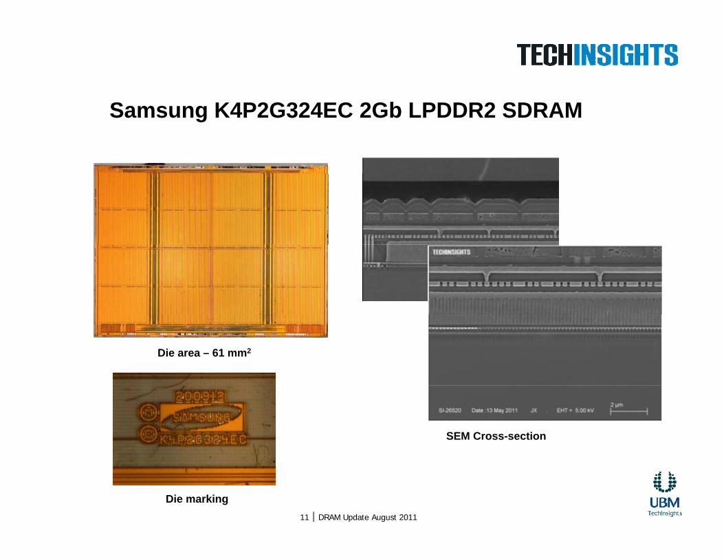
S K4P2G324EC 2Gb LPDDR2 SDRAMSamsung K4P2G324EC 2Gb LPDDR2 SDRAM
Die area – 61 mm2
SEM Cross-section
Die marking11 I DRAM Update August 2011
S K3PE7E700B L P DDR2 SDRAMSamsung K3PE7E700B Low Power DDR2 SDRAM
• Found in a package-on-package (PoP) with the Exynos processor from Samsung’s new Galaxy phones.
• Identified by ‘4G-B-MP’ die marking• 4Gb LPDDR2 SDRAM manufactured at the 30nm-class
process node
Available reports:• IC Review of the Samsung K3PE7E700B LPDDR2
SDRAMCi itVi i A l i th S 30 l• CircuitVision Analysis on the Samsung 30nm-class 4Gbit LPDDR2 SDRAM – Available Nov 2011
• Further analysis available on requestFurther analysis available on request
1212 I DRAM Update August 2011
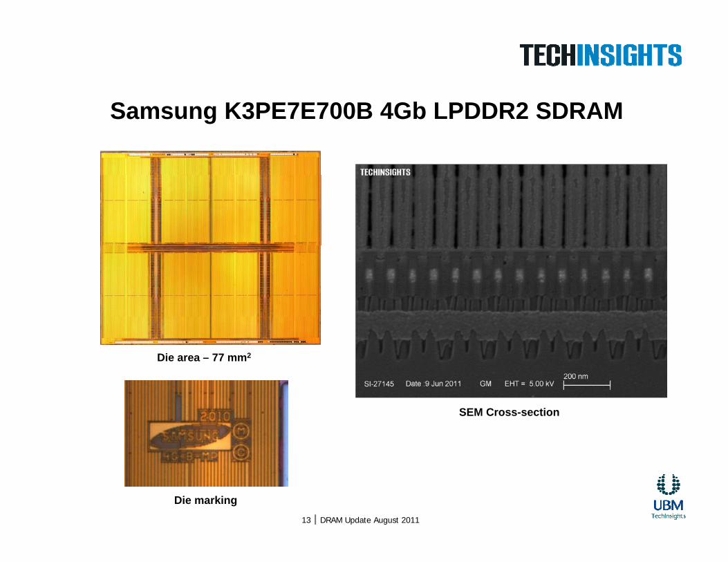
S K3PE7E700B 4Gb LPDDR2 SDRAMSamsung K3PE7E700B 4Gb LPDDR2 SDRAM
Die area – 77 mm2
SEM Cross-section
Die marking13 I DRAM Update August 2011
DDR3 SDRAM
S K4B2G0846D DDR3 SDRAMSamsung K4B2G0846D DDR3 SDRAM
• Located on DDR3 DIMM module.• Identified by ‘K4B2G0846D’ die marking• 2Gb DDR3 SDRAM manufactured at the 30nm-class process
node
Available reports:• IC Review of the Samsung K4B2G0846D DDR3IC Review of the Samsung K4B2G0846D DDR3
SDRAM• CircuitVision Analysis on the Samsung
K4B2G0846D 30nm-class 2Gbit DDR3 SDRAM• Memory Detailed Structural Analysis on the
Samsung K4B2G0846D 30nm-class 2Gbit DDR3Samsung K4B2G0846D 30nm class 2Gbit DDR3 DRAM
1515 I DRAM Update August 2011
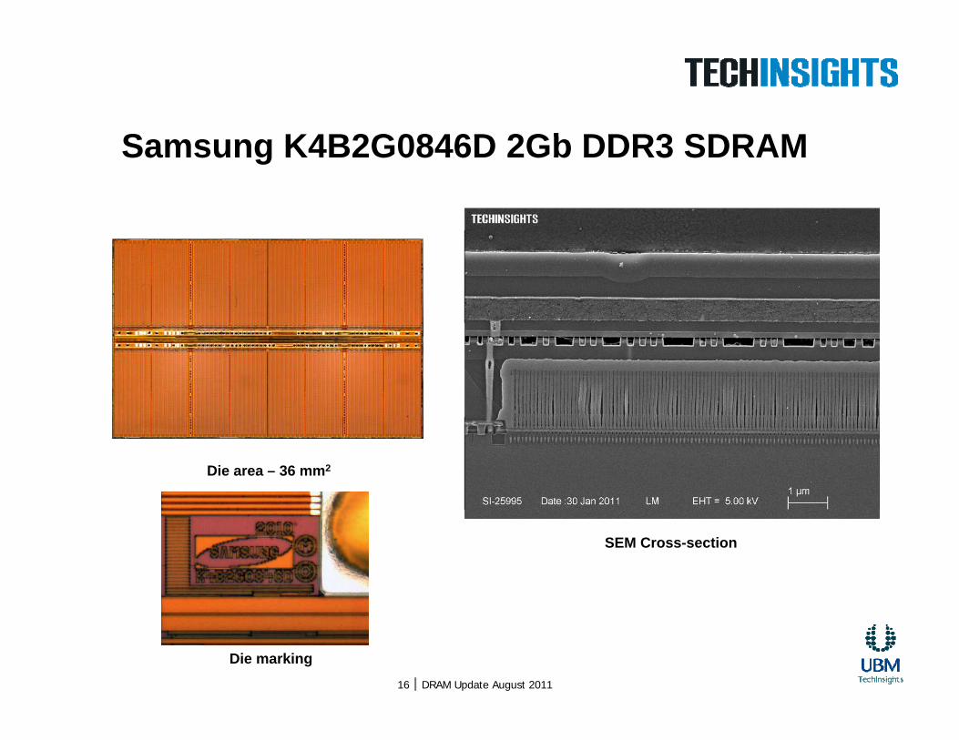
S K4B2G0846D 2Gb DDR3 SDRAMSamsung K4B2G0846D 2Gb DDR3 SDRAM
Die area – 36 mm2
SEM Cross-section
Die marking16 I DRAM Update August 2011
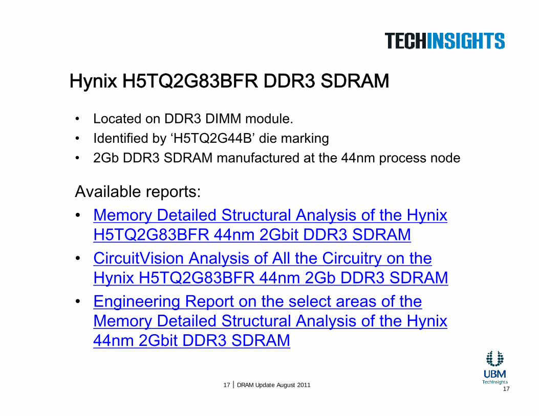
H i H5TQ2G83BFR DDR3 SDRAMHynix H5TQ2G83BFR DDR3 SDRAM
• Located on DDR3 DIMM module.• Identified by ‘H5TQ2G44B’ die marking• 2Gb DDR3 SDRAM manufactured at the 44nm process node
Available reports:• Memory Detailed Structural Analysis of the Hynix
H5TQ2G83BFR 44nm 2Gbit DDR3 SDRAMH5TQ2G83BFR 44nm 2Gbit DDR3 SDRAM• CircuitVision Analysis of All the Circuitry on the
Hynix H5TQ2G83BFR 44nm 2Gb DDR3 SDRAM• Engineering Report on the select areas of the
Memory Detailed Structural Analysis of the Hynix 44nm 2Gbit DDR3 SDRAM44nm 2Gbit DDR3 SDRAM
1717 I DRAM Update August 2011
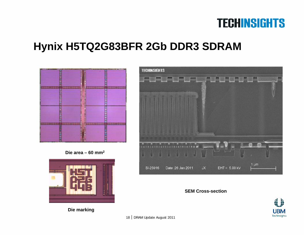
H i H5TQ2G83BFR 2Gb DDR3 SDRAMHynix H5TQ2G83BFR 2Gb DDR3 SDRAM
Die area – 60 mm2
SEM Cross-section
Die marking
SEM Cross-section
18 I DRAM Update August 2011

El id J2108BCSE DDR3 SDRAMElpida J2108BCSE DDR3 SDRAM
• Located on DDR3 DIMM module.• Identified by ‘J2108BC’ die marking• 2Gb DDR3 SDRAM manufactured at the 44nm process node
Available reports:• IC Review of the Elpida J2108BCSE-DJ-F DDR3
F th l i il bl t• Further analysis available upon request
1919 I DRAM Update August 2011
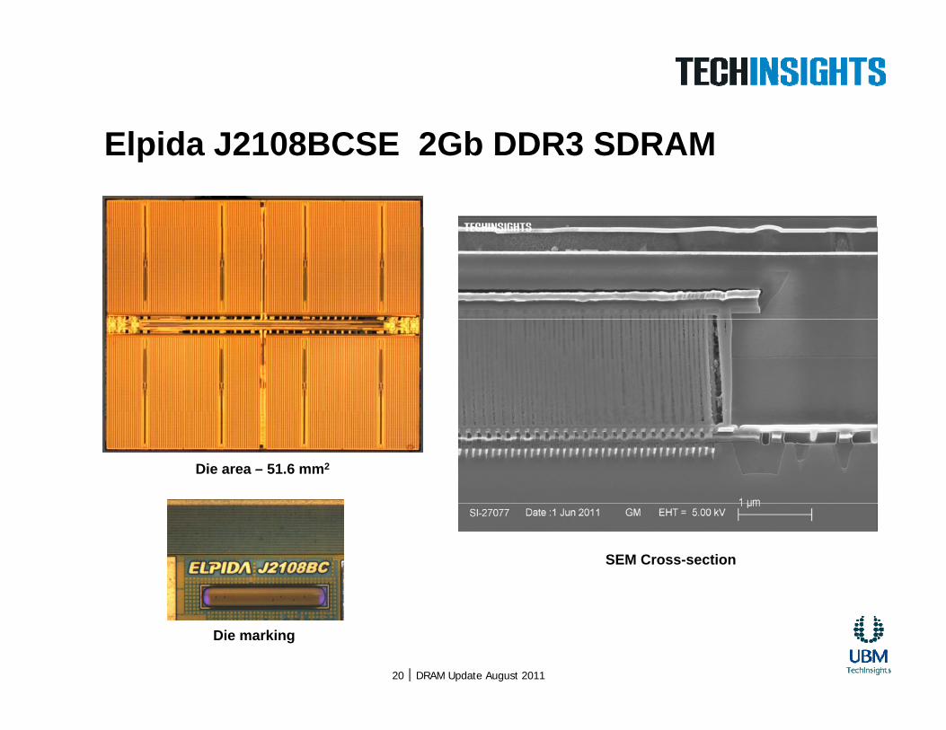
El id J2108BCSE 2Gb DDR3 SDRAMElpida J2108BCSE 2Gb DDR3 SDRAM
Die area – 51.6 mm2
SEM Cross-section
Die marking
20 I DRAM Update August 2011
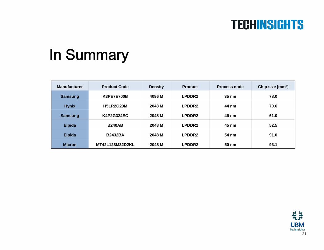
In Summary
Manufacturer Product Code Density Product Process node Chip size [mm2]
Samsung K3PE7E700B 4096 M LPDDR2 35 nm 78.0
Hynix H5LR2G23M 2048 M LPDDR2 44 nm 70.6
Samsung K4P2G324EC 2048 M LPDDR2 46 nm 61.0
Elpida B240AB 2048 M LPDDR2 45 nm 52.5
Elpida B2432BA 2048 M LPDDR2 54 nm 91.0
Micron MT42L128M32D2KL 2048 M LPDDR2 50 nm 93.1
21

If you are interested in finding out more about UBM TechInsights’ library ofabout UBM TechInsights library of DRAM reports and upcoming analyses, please contact:please contact:
Cindy Lin, Director of SalesT: 886 2 77072799E: [email protected]
22