a coin detection system by coupled printed spiral … coin detection system by coupled printed...
TRANSCRIPT

A Coin Detection System by Coupled Printed Spiral Inductors
Junichi Fukatani∗, Sho Yamaguchi∗, Masayuki Yamauchi†, Kazuhisa Yoshimatsu†, Hisashi Aomori∗ and Mamoru Tanaka∗∗Department of Electrical and Electronics Engineering, Sophia University
7-1 Kioi, Chiyoda-ku, Tokyo, 102-8554, JAPAN†Department of Electronics and Computer Engineering, Hiroshima Institute of Technology University
2-1-1 Miwake, Saeki-ku, Hiroshima-shi, Hiroshima, 731-5193, [email protected], [email protected], [email protected],
[email protected], [email protected], [email protected]
Abstract: This paper describes a coin detection system using coupled Printed Spiral Inductors (PS-Inductors). Inthis research, the PS-Inductor is composed of copper foil spiral on the printed board. As an advantages, the PS-Inductor can be made easily and does not need the iron core. The experimental measurement and the theoreticalcalculation of the inductance of the PS-Inductor are derived. This enables the easily realizable coin detectionsystem using PS-Inductor. In this system, a coin can be identified as changes of the mutual inductance of coupledPS-Inductors. The mutual inductance is investigated by inserting the coin between two PS-Inductors.
Key–Words: Coin detection, Mutual inductance, Printed Spiral Inductor, Combination inductance, Self-inductance
1 Introduction
A lot of spiral shape elements are used for RFID, IC,and so on [1][2]. Especially, the spiral shapes in-ductors are called spiral-inductor. The spiral induc-tor which is generated in an IC is often used [3]. Thespiral inductor is not only constructed on the chip butalso on a printed board. The spiral inductors on theprinted board have been easily used as a mutual in-ductor because the iron core does not need. That is,the mutual inductance can be easily achieved.
In this paper, we propose a novel coin detectionsystem using the mutual inductance changes of cou-pled printed spiral inductors (PS-Inductors). Sincethe elemental composition of each coin in the worldis unique, the influence of the electro magnetic fieldgenerated by two PS-Inductors, strongly depends onthe coin type. In other words, the coin can be iden-tified by investigating the mutual inductance changesof two PS-Inductors. The advantage of the proposedmethod is that this method is better realizable than theconventional coin detection system using the naturalfrequency of coin that requires the Fourier transformfor detection [4]. Moreover, it can be said that the PS-Inductor generated by semicircular wiring pattern inthe printed board is fit for the physical characteristicof coins.
The experimental results of various coins suggestthat the proposed method can identify coins correctly.
This paper is organized as follows. In Section 2,the evaluation of the inductance of the PS-Inductor isdescribed. The self inductance L is measured and cal-
culated. In Section 3, the coin identification systemis proposed. The coin can be distinguished by usingthe mutual inductance change effected by it. Section4 shows the experimental methods and results usingtwo coupled PS-Inductors. The coin identification isexperimented using two types of PS-Inductors whichhave different diameter. Finally, in Section 5 the con-clusion of this paper are drawn.
2 Printed Spiral Inductor
The PS-Inductor is designed by combining hemicy-cles. In general, a spiral inductor in an IC is com-posed of a square wiring pattern that is combinationof straight lines.
The circle wiring pattern can provide the high Qvalue [5]. Therefore, PS-Inductor with circle wiringpattern is decided in this paper. Besides, its physicalform suits to form of coins very well. The layout andinductance of PS-Inductor are decided by five param-eters as shown in Fig. 1 and Table 1. Also, two typesof PS-Inductor α and β are used in this research (seeFig. 2). The PS-Inductors are created by combiningsemicircular patterns by using cutting machine (seeFig. 3). The length of the conductor shortens towardthe center because the conductor rolls the hemicyclefrom the maximum radius to the center.
WSEAS TRANSACTIONS on CIRCUITS and SYSTEMS
Fukatani, Yamaguchi, Yamauchi, Yoshimatsu, Aomori and Tanaka
ISSN: 1109-2734 832 Issue 8, Volume 7, August 2008

maxRw
d
Figure 1: Design of PS-Inductor.
Table 1: Parameters of two kinds of PS-Inductor
α β
Greatest diameter Rmax 36[mm] 10[mm]Pattern distance d 0.2[mm] 0.11[mm]Pattern width w 0.1[mm] 0.09[mm]
Number of harf-turn TR 80[half-turn] 30[half-turn]Pattern thickness 35[um] 35[um]
(single-sided)Pattern thickness 9[um] 9[um](double-sided)Board material Glass epoxy Glass epoxy
2.1 Measurement of self-inductance of thePS-Inductor
There are many methods of the measurement induc-tance. In this research, the inductance is measured byoscillating system which is built by combining arbi-trary capacitors to a PS-Inductor. When the LC oscil-lation is caused, an inductance is obtained from an os-cillation frequency and the capacitances. The oscilla-tion frequency can be changed by changing values ofcapacitors. Therefore, the inductance of PS-Inductorcan be determined by some experiments.
2.1.1 Experimental measurement of self-inductance
An inductance of high accuracy can not be obtainedwithout an oscillation frequency and capacitances ofhigh accuracy. Therefore, when the inductance ismeasured, a parasitic impedance must be consideredby all possible means in the experiment circuit andthe calculation obataining the inductance. The Col-
PS-Inductor α
PS-Inductor β
Figure 2: Picture of PS-Inductor α and PS-Inductor β
cutting
copper foil
base material
Figure 3: Fabrication of PS-Inductor
pitts oscillator which uses only one bipolar transis-tor is used because the influences of the parasiticimpedances are reduced easily. Only a digital oscil-loscope is used for the frequency measurements andwaveform observations. Therefore, a circuit modelwith the measurement instrument can be drawn as likeFig. 4. An equivalent circuit of measuring impedance(see Table 2) is shown in the frame of Fig. 4. If os-cillation waveform is sinusoidal shape, an inductancecan be obtained from some capacitors, some resistors,an inductors, and an oscillation frequency by usingfollowing equations.
B
Measuring Impedance
ProbeOscillo-Scope
Z1Z2Z3Z4
L
RL
R2 A
R1
C1
C2
C3
c1 c2
L'r1
r2C4
R3
Figure 4: The circuit model with equivalent circuit ofmeasurement equipments.
WSEAS TRANSACTIONS on CIRCUITS and SYSTEMS
Fukatani, Yamaguchi, Yamauchi, Yoshimatsu, Aomori and Tanaka
ISSN: 1109-2734 833 Issue 8, Volume 7, August 2008

[MHz]f0
L[uH
]
30
35
40
45
50
55
60
65
70
0.7 0.8 0.9 1 1.1 1.2 1.3 1.4 1.5
Figure 5: The inductance L vs oscillating frequencyf0 using PS-Inductor α
L =1 +√
1 − 4η2R2
2ωη, (1)
where
η = ωC4 − ζ
ε2 + ζ2,
ε =αR3 + ω
2βδ
α2 + ω2β2,
ζ = − 1ω
(1
C1+
1C3
) +ω(αδ − βγ)α2 + ω2β2
α = 1 − ω2(r1 + r2)R3c2(c1 +C2) − ω2c2L′,
β = R3(c1 + c2 +C2) + c2(r1 + r2) − ω2L′R3c2(c1 +C2),
γ = R3 − ω2c2R3L′ , δ = (r1 + r2)c2R3 ,
The Eq. (1) can be obtained by following equa-tions and the oscillation condition.
Z1 =1
jωc1 +1
r1+ jωL′+r2+1
jωc2
,
Z2 =1
1R3+ 1
Z1
,
Z3 =1
1Z2+ jωC2
=γ + jωδα + jωβ
,
Z4 =1
jωC1+
1jωC3
+1Z3= ε + jζ
Y =R − jωL
R2 + ω2L2+ jωC4 +
1Z4
Im{Y} = 0.
(2)
The Y expresses an admittance of whole circuit. Theoscillation frequency f0 is measured while changing
Table 2: The value of parasitic element (1) modelnumber
(1) impedance
oscilloscope SS-7804 C2 = 25[pF]454/L/VL C2 = 16[pF]DS-9242A R = 1[MΩ]
probe SS-0110 C1 =170[pF]r1 + r2 =166.73[Ω]L′ =140[uH]
SS-101R C1 =12[pF]r1 + r2 =9.002738[MΩ]L′ =140[uH]
PP002i C1 = 15.5[pF]r1 + r2 =9.05[MΩ]L′ =140[uH]
transistor 2SC4083 0.8[pF]
Table 3: The Inductance of PS-Inductor
Parameter of Actual Calculated errorPS-Inductor measurement value [%]
α 31.944[uH] 31.265[uH] 2.17β 1.771[uH] 1.806[uH] 1.94
the capacitors C1, C2, C3, and C4. Figure 5 showsthe results using Eqs. (1) and (2). The inductance Lis approached to the constant value. Therefore, theinductance using Eqs. (1) and (2) is assumed as themeasurement value in this research.
2.1.2 Validation of experimental measurement
An inductance is calculated as follows:
L =Φ(t)i(t)
(3)
In our previous study, we developed a simulatorwhich calculates the magnetic flux by using Biot-Savart Law and finite element method, and calculatesan inductance of a PS-Inductor [6]. In this method,magnetic flux at an arbitrary domain “AT” of spacingis calculated from an arbitrary domain “SC” ofconductor of the PS-Inductor below sequences.
1. Magnetic flux density of a point “a” included do-main AT, and magnetic flux density of a point “b”
WSEAS TRANSACTIONS on CIRCUITS and SYSTEMS
Fukatani, Yamaguchi, Yamauchi, Yoshimatsu, Aomori and Tanaka
ISSN: 1109-2734 834 Issue 8, Volume 7, August 2008
a
b AT
Metal
A
Center
Magnetic field between these two dot lines is not calculated.
SC
Figure 6: Analysis of inside
included domain AT are calculated from a point“A” included domain SC by using Biot-SavartLaw (see Fig. 6).
2. An average of these magnetic flux densities iscalculated.
3. The magnetic flux of AT is calculated by multi-plying the average by a square measure of AT.
The magnetic flux of AT is obtained by applyingfor whole conductor, and an inductance of the PS-Inductor is calculated by applying for whole spac-ing. In this method, the averages of magnetic flux arecalculated, because computation time becomes shortand accuracy becomes good. The calculated values ofself-inductances of PS-Inductor α and β are shown inTable 3.
3 Coin Identification System
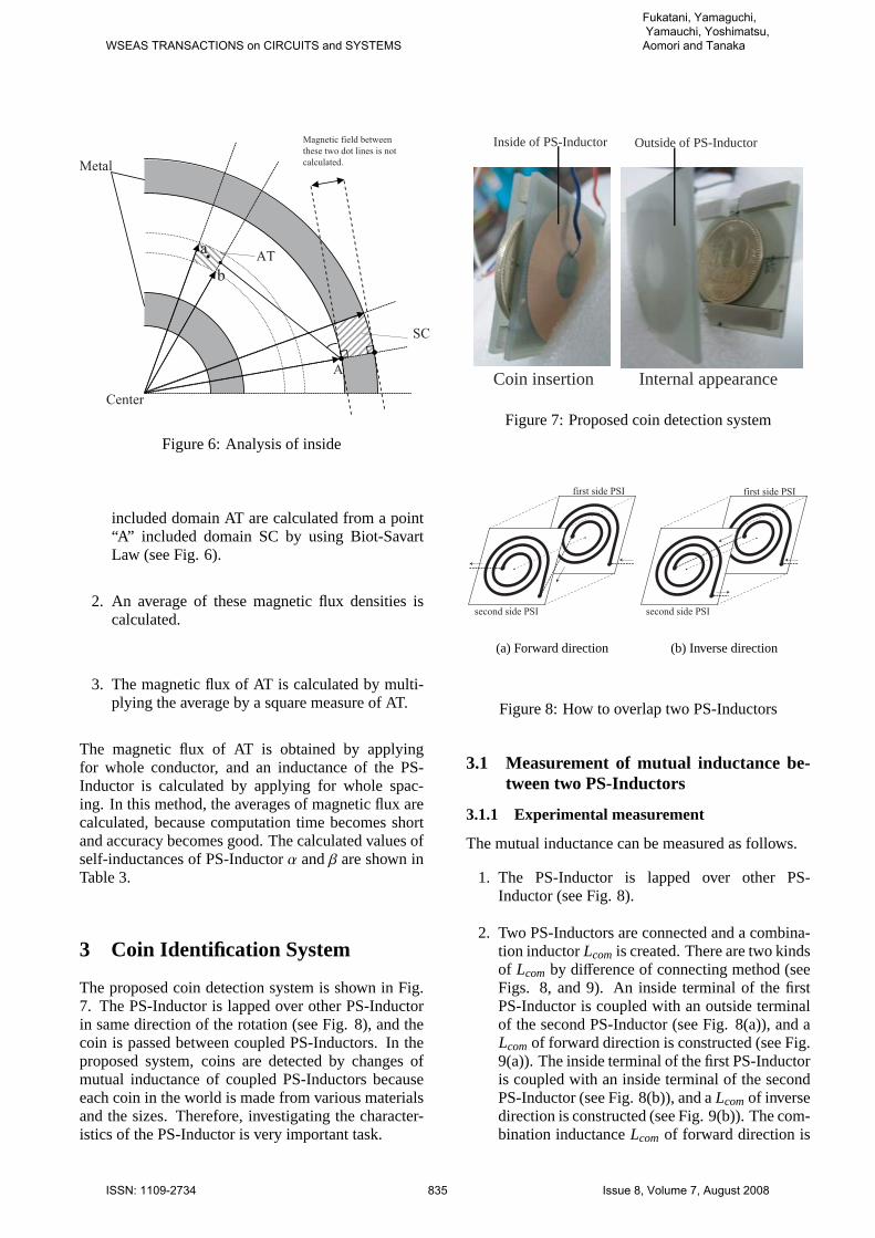
The proposed coin detection system is shown in Fig.7. The PS-Inductor is lapped over other PS-Inductorin same direction of the rotation (see Fig. 8), and thecoin is passed between coupled PS-Inductors. In theproposed system, coins are detected by changes ofmutual inductance of coupled PS-Inductors becauseeach coin in the world is made from various materialsand the sizes. Therefore, investigating the character-istics of the PS-Inductor is very important task.
Coin insertion Internal appearance
Inside of PS-Inductor Outside of PS-Inductor
Figure 7: Proposed coin detection system
first side PSI
second side PSI
(a) Forward direction
first side PSI
second side PSI
(b) Inverse direction
Figure 8: How to overlap two PS-Inductors
3.1 Measurement of mutual inductance be-tween two PS-Inductors
3.1.1 Experimental measurement
The mutual inductance can be measured as follows.
1. The PS-Inductor is lapped over other PS-Inductor (see Fig. 8).
2. Two PS-Inductors are connected and a combina-tion inductor Lcom is created. There are two kindsof Lcom by difference of connecting method (seeFigs. 8, and 9). An inside terminal of the firstPS-Inductor is coupled with an outside terminalof the second PS-Inductor (see Fig. 8(a)), and aLcom of forward direction is constructed (see Fig.9(a)). The inside terminal of the first PS-Inductoris coupled with an inside terminal of the secondPS-Inductor (see Fig. 8(b)), and a Lcom of inversedirection is constructed (see Fig. 9(b)). The com-bination inductance Lcom of forward direction is
WSEAS TRANSACTIONS on CIRCUITS and SYSTEMS
Fukatani, Yamaguchi, Yamauchi, Yoshimatsu, Aomori and Tanaka
ISSN: 1109-2734 835 Issue 8, Volume 7, August 2008

(a) Forward direction (b) Inverse direction
Figure 9: Combination inductance circuit
given by
v = L1didt+ M
didt+ L2
didt+ M
didt
= (L1 + L2 + 2M)didt,
Lcom = L1 + L2 + 2M,
(4)
and the combination inductance Lcom of inversedirection is obtained by
v = L1didt− M
didt+ L2
didt− M
didt
= (L1 + L2 − 2M)didt,
Lcom = L1 + L2 − 2M.
(5)
Therefore, the mutual inductance M is describedby
M =|Lcom − L1 − L2|
2. (6)
This proposed system uses the Lcom of forwarddirection, because the Lcom of forward directionis larger than that of inverse direction, and mea-surement of forward direction is easier than thatof inverse direction. Therefore, we focus on onlyLcom of the forward direction.
3. The measurement circuit uses the Colpitts-oscillator shown in Fig. 10. The distancebetween the first PS-Inductor and the secondPS-Inductor is expressed as “d”. The thick-ness of PS-Inductor’s base is expressed as “t”and t=0.0015[m]. A Collpitts-oscillator is con-structed using the Lcom. Two terminals of theLcom are connected with a terminal “A”, and a ter-minal “B”. The combination inductance is mea-sured by the oscillation method using a Colpitts-oscillator. From Eq. (1), the combination induc-tance is calculated as
Self-inductance
second side PSI
first side PSI
Mutual inductance
Figure 11: Three dimensional calculation
Lcom =1 +√
1 − 4η2RLcom2
2ωη, (7)
where the RLcom expresses a resistance including inthe Lcom.
3.1.2 Theoretical approach
In [7], Nukushida et.al. proposed a new method fortheoretical calculation of the mutual inductance by us-ing the Biot-Savart law and finite element method.The calculation method is changed to three dimen-sional calculation from previous simulator which iscomposed of two dimensional calculation (see Fig.11). The new simulator obtains the sum of a self in-ductance and a mutual inductance (L + M). The mu-tual inductance is calculated by subtracting self induc-tance L that is obtained by previous method.
3.1.3 Validation checking of experimental mea-surement
We experiment using two coupled PS-Inductors (seeTable 1) and Colpitts-oscillator circuit (see Fig. 10).The distance d of coupled PS-Inductors α is changedinto 0.0025, 0.0035, 0.0045, 0.0055 and 0.0065 [m]and coupled PS-Inductors β is changed into 0.002,0.003, 0.004, 0.005 ,0.006 and 0.007 [m]. The mu-tual inductance M and combination inductance Lcomare measured in each distance. Then we compare ac-tual measurement results with theoretical calculationresults (see Figs. 12 and 13, and Tables 4, 5, 6 and 7).
The relative error margin [%] of the combinationinductance Lcom is smaller than that of the mutual in-
WSEAS TRANSACTIONS on CIRCUITS and SYSTEMS
Fukatani, Yamaguchi, Yamauchi, Yoshimatsu, Aomori and Tanaka
ISSN: 1109-2734 836 Issue 8, Volume 7, August 2008

Z1Z2Z3
d
t B
Measuring Impedance
ProbeOscillo-Scope
Z1Z2Z3Z4
R2 A
R1
C1
C2
C3
c1 c2
L'r1
r2C4
R3
Lcom
RL1 RL2
L2L1
Figure 10: Coupled PS-Inductors and Colpitts-oscillator circuit
Table 4: Error of the Combination inductance Lcom
using PS-Inductor α (1)experimental measurementLcom[μH] (2)theoretical calculation Lcal[μH]
distance d[m] (1) (2) error
0.0025 114.8 112.7 2.10.0035 109.8 107.3 2.50.0045 106.2 106.0 0.20.0055 100.5 98.53 1.970.0065 99.23 93.34 5.89
ductance M. In the PS-Inductor β, a large margin oferror [%] especially appears to the mutual inductance.As the reason, the mutual inductance of PS-Inductorβ is small. Therefore, this system should be made inthe range of which distance d is small.
4 ExperimentsIn order to evaluate the coin identification perfor-mance, we apply our system to 10 coins (see Fig. 14,and Table 8); JPY (500, 100, 50, 10, 5 and 1) and USD(quarter, dime, nickel and penny).
Firstly, the PS-Inductor α is used. The measure-ment conditions are set as follows. As shown in Figs.15, x − y coordinates are fixed to the second side PS-
Table 5: Error of the Mutual inductance M of PS-Inductor α (1)experimental measurement Mmea[μH](2)theoretical calculation Mcal[μH]
distance d[m] (1) (2) error
0.0025 22.21 22.77 0.560.0035 19.71 20.07 0.360.0045 17.92 19.40 1.480.0055 15.06 15.68 0.620.0065 14.44 13.09 1.35
Inductor. These coordinate are decided based on theside of the 500-yen coin, because the 500-yen coin hasthe largest radius in ten kinds of coins. The Rmax, xmaxand d are fixed as 0.018 [m], 0.03125 [m], and 0.0045[m] respectively, because the radius of 500-yen coinis 0.01325 [m]. The center of the 500-yen coin runsthrow the origin coordinate of x-axis and y-axis. InFig. 10, the resistances R1, R2, and R3 are fixed as 10[kΩ], 10 [kΩ], and 3.3 [kΩ] respectively. The capaci-tors C1, C2, C3, and C4 are changed as shown in Table9 and measured at each parameter. Measurement val-ues are assumed an average of three values. The x ex-pressing the position of coin is changed to -0.03125,-0.018, -0.012, -0.009, -0.006, -0.003, 0, 0.003, 0.006,0.009, 0.012, 0.018, and 0.03125 [m], and mutual in-
WSEAS TRANSACTIONS on CIRCUITS and SYSTEMS
Fukatani, Yamaguchi, Yamauchi, Yoshimatsu, Aomori and Tanaka
ISSN: 1109-2734 837 Issue 8, Volume 7, August 2008

Distance d[m]
Mut
ual i
nduc
tanc
e M
, Com
bina
tion
indu
ctan
ce Lcom
[μH
]
0
20
40
60
80
100
120
140
0.002 0.0025 0.003 0.0035 0.004 0.0045 0.005 0.0055 0.006 0.0065 0.007
Actual measurement(Mutual)
Simulation(Mutual)Actual measurement(Combination)
Simulation(Combination)
Figure 12: Distance d v.s. Mutual inductance M andCombination inductance Lcom using PS-Inductor α
ductance and combination inductance are measuredat each position of the 500-yen coin. As a result ofFig. 16, mutual inductance and combination induc-tance have a minimum value around x=0. For this rea-son, the x is changed to 0, 0.003, 0.006, 0.012, 0.018,and 0.03125[m] (see Fig. 17), and mutual inductanceis measured at each position by ten coins. Fig. 18shows changing of mutual inductances by changed ofposition of each coin. Therefore, the coin can be pre-dicted by this result. Especially, many kind of the coincan be easily predicted around x=0.
Next, we use the PS-Inductor β. When thediameter of PS-Inductor is smaller than the averagediameter of coins, we try constructing coin detectionsystem. Some measurement conditions are changedfrom above conditions as follows. The distance d isfixed as 0.003 [m] and 0.005 [m]. In Fig. 10, thecapacitors C1, C2, C3, and C4 are changed as shown
Table 6: Error of the Combination inductance Lcom
using PS-Inductor β (1)experimental measurementLcom[μH] (2)theoretical calculation Lcal[μH]
distance d[m] (1) (2) error
0.002 4.33 5.28 0.950.003 4.23 4.94 0.710.004 4.00 4.73 0.730.005 3.92 4.60 0.680.006 3.81 4.51 0.70.007 3.70 4.45 0.75
Table 7: Error of the Mutual inductance M of PS-Inductor β (1)experimental measurement Mmea[μH](2)theoretical calculation Mcal[μH]
distance d[m] (1) (2) error
0.002 0.3955 0.4616 0.06610.003 0.3459 0.2933 0.05260.004 0.2276 0.1888 0.03880.005 0.1893 0.1224 0.06690.006 0.1323 0.0791 0.05320.007 0.0788 0.0501 0.0287
Mut
ual i
nduc
tanc
e M
, Com
bina
tion
indu
ctan
ce Lcom
[μH
]
Distance d[m]
0
0.5
1
1.5
2
2.5
3
3.5
4
4.5
5
0.002 0.0025 0.003 0.0035 0.004 0.0045 0.005 0.0055 0.006 0.0065 0.007
Actual measurement(Mutual)
Simulation(Mutual)Actual measurement(Combination)
Simulation(Combination)
Figure 13: Distance d v.s. Mutual inductance M andCombination inductance Lcom using PS-Inductor β
in Table 10 and measured at each value. Measurementvalues are assumed an average of four values. Otherconditions are not changed from above conditions.Figure 19 and 20 show the results. The coin can bepredicted only d≤0.003 [m]. However, from the viewpoint obtained by Fig.20, it is difficult to identify thecoins. Because the diameter of the PS-Inductor issmall, the mutual inductance is small.
The coin can be predicted by the PS-Inductorespecially around x=0. Furthermore, in other words,a position, a velocity, and a direction of the coincan be predicted by these results, if a kind of thecoin is known, and when the coin is running throughbetween PS-Inductors.
WSEAS TRANSACTIONS on CIRCUITS and SYSTEMS
Fukatani, Yamaguchi, Yamauchi, Yoshimatsu, Aomori and Tanaka
ISSN: 1109-2734 838 Issue 8, Volume 7, August 2008

yen yenyen yenyen yencent centcent cent
Coin position based on the 500-yen coin: x[m](y=0)
Mut
ual i
nduc
tanc
e[μH
]
Coin identification is easy when a difference is great.
Figure 18: Coins identification of mutual inductance using PS-Inductor α
Figure 14: 10coins (JPY (500, 100, 50, 10, 5, 1) andUSD (penny, nickel, dime, quarter))
5 Conclusion
In this paper, we proposed a novel coin detection sys-tem using coupled PS-Inductors. The experimental re-sults were shown that our method can identify the 10coins correctly. This method can identify the coins invery simple way that transition of mutual inductancebetween PS-Inductors by inserting the coin is only in-vestigated. The coin identification was possible evenby the PS-Inductor that is smaller than the coin. How-ever, prediction of the kind of coin became easy by
Table 8: Details of coin (1)outside diameter[mm](2)thickness[mm]
coin (1) (2) material
500yen 26.5 2.0 72[%]Cu, 20[%]Zn,8[%]Ni
100yen 22.6 1.7 75[%]Cu, 25[%]Ni50yen 21 1.5 75[%]Cu, 25[%]Ni10yen 23.5 1.3 95[%]Cu, 3-4[%]Zn,
1-2[%]Sn5yen 22 1.5 60-70[%]Cu,
30-40[%]Zn1yen 20 1.54 100[%]Al1cent 19.05 1.55 97.5[%]Zn, 2.5[%]Cu5cent 21.21 1.95 75[%]Cu, 25[%]Ni10cent 17.91 1.35 91.67[%]Cu, 8.33[%]Ni25cent 24.26 1.75 91.66[%]Cu, 8.34[%]Ni
using the PS-Inductor of diameter that is larger thandiameters of coins. Moreover, prediction of the kind
WSEAS TRANSACTIONS on CIRCUITS and SYSTEMS
Fukatani, Yamaguchi, Yamauchi, Yoshimatsu, Aomori and Tanaka
ISSN: 1109-2734 839 Issue 8, Volume 7, August 2008

0
0.2
0.4
0.6
0.8
1
1.2
1.4
1.6
0 0.005 0.01 0.015 0.02 0.025 0.03 0.035
500yen 100yen
50yen 10yen
5yen 1yen
1cent 5cent
10cent 25cent
Coin position based on the 500-yen coin: x[m](y=0)
Mut
ual i
nduc
tanc
e[μH
]
Figure 19: Coins identification of mutual inductance using PS-Inductor β d=0.003
Table 9: Combination of capacitors using parameter α(1)Combination
(1) C1[pF] C2[pF] C3[pF] C4[pF]
(γ) 4700 200 4700 100(δ) 4700 200 9400 100(ε) 6920 200 9400 100
Table 10: Combination of capacitors using parameterβ (1)Combination
(1) C1[pF] C2[pF] C3[pF] C4[pF]
(ζ) 100 20 20 1(η) 100 20 20 2(θ) 470 20 20 2(ι) 470 20 20 6
of coin became clear when the distance d between twoPS-Inductor is short.
It can be said that a very small coin identification
y
x
Rmax
y
Outside of the second side PS-InductorInside of the second side PS-Inductor
Figure 15: x − y coordinates
system at the stamp level can be constructed.
Acknowledgment
This research is supported by the fund of the OpenResearch Center Project from MEXT of the JapaneseGovernment (2007-2011). This research is sup-ported by the Grants-in-Aid for Young Scientific Re-search(B) (No. 19760270) from the Japan Society forthe Promotion of Science.
WSEAS TRANSACTIONS on CIRCUITS and SYSTEMS
Fukatani, Yamaguchi, Yamauchi, Yoshimatsu, Aomori and Tanaka
ISSN: 1109-2734 840 Issue 8, Volume 7, August 2008

0.3
0.4
0.5
0.6
0.7
0.8
0.9
1
1.1
1.2
1.3
0 0.005 0.01 0.015 0.02 0.025 0.03 0.035
500yen 100yen
50yen 10yen
5yen 1yen
1cent 5cent
10cent 25cent
Coin position based on the 500-yen coin: x[m](y=0)
Mut
ual i
nduc
tanc
e[μH
]
Figure 20: Coins identification of mutual inductance using PS-Inductor β d=0.005
Coin position based on the 500-yen coin: x[m](y=0)Mut
ual i
nduc
tanc
e M
, C
ombi
natio
n in
duct
ance
Lcom
[μH
]
-20
0
20
40
60
80
100
120
-0.04 -0.03 -0.02 -0.01 0 0.01 0.02 0.03 0.04
Combination inductance
Mutual inductance
Figure 16: Characteristic by the 500-yen coin
References:
[1] J. Park, Y. Park, Y. Kim, S. Jun, “A ResistanceDeviation-to-Time Interval Converter and itsApplication to a Passive RFID Tag for Security,”World Scientific and Engineering Academy andSociety(WSEAS) Circuits, Theory, and Applica-tions, Vol.1, pp.126-130, July 2007.
[2] A. Kabir, K. C. Huang, R. Wu, P. Rapajic, “NextGeneration Identity Card: RFID-based Auto-
matic Access Control System for Universities,”World Scientific and Engineering Academy andSociety(WSEAS) Selected Topics on Circuits,Systems, Electronics, Control and Signal pro-cessing, pp.480-483, December 2007.
[3] K. Okada, “Design Optimization Methodologyfor On-Chip Spiral Inductors,” IEICE Trans.Electron., Vol.E87-C, no.6, June, 2004.
[4] M. Suzuki, “Development of a simple and non-destructive examination for counterfeit coins us-ing acoustic characteristics,” Forensic ScienceInternational, Vol.177, Issue 1, pp.e5-e8, May2008.
[5] S. S. Mohan, “Simple Accurate Expressionsfor Planar Spiral Inductances,” IEEE Journalof solid-state circuits., Vol.37, no.10, October,1999.
[6] M. Motoyoshi, Y. Tanaka, M. Yamauchi and M.Tanaka, “Measurement and Numeric Calcula-tionfor Printed Spiral Inductors,” Proc. of Non-linear Theory and its Applications 2005, pp.290-293, 2005.
[7] M. Nukushina, T. Kunihiro, T. Nanko, M. Ya-mauchi and M. Tanaka, “Synchronization Phe-nomena of Coupled Colpitts Oscillators usingPrinted Spiral Inductors,” Proc. of Nonlinear
WSEAS TRANSACTIONS on CIRCUITS and SYSTEMS
Fukatani, Yamaguchi, Yamauchi, Yoshimatsu, Aomori and Tanaka
ISSN: 1109-2734 841 Issue 8, Volume 7, August 2008

x=0
x
y
r
y
x
x=0.006
x=0.018
y
x
x=0.003
x
y
x=0.012
x
x
y
x=0.03125
Figure 17: Setting of coordinates based on the 500-yen coin
Theory and its Applications 2007, pp.325-328,2007.
[8] J. Fukatani, S. Yamaguchi, M. Yamauchi, H. Ao-mori and M. Tanaka, “A Coin Detection Systemby Coupled Printed Spiral Inductors””, WorldScientific and Engineering Academy and Soci-ety(WSEAS) New aspects of circuits, pp.91-95,July 2008
[9] H.G. Dill, “Designing Inductors for Thin FilmApplications,” Electronic Design, pp.52-59,1964.
[10] S. Y. Y. Leung and D.C.C. Lam, “Performanceof Printed Polymer-Based RFID Antenna onCurvilinear Surface,” IEEE CPMT Transactionsin Electronic Packaging Manufacturing, Vol.30,no.3, pp.200-205, July 2007.
[11] F. J. Schmuckle, “The method of lines forthe analysis of rectangular spiral inductors [inMMICs],” Microwave Theory and Techniques,IEEE Transactions on , Vol.41 , Issue6, pp.1183-118y6, June-July 1993.
[12] M. H. Chiou, “A new wideband modeling tech-nique for spiral inductors,” Semiconductor De-vice Research Symposium, 2003 International,pp.290-291, December 2003.
[13] R. D. Lutz, “Modeling of spiral inductors onlossy substrates for RFIC applications,” RadioFrequency Integrated Circuits (RFIC) Sympo-sium, 1998 IEEE, pp.313-316, 7-9 June 1998.
WSEAS TRANSACTIONS on CIRCUITS and SYSTEMS
Fukatani, Yamaguchi, Yamauchi, Yoshimatsu, Aomori and Tanaka
ISSN: 1109-2734 842 Issue 8, Volume 7, August 2008