a comprehensive review of zno materials and devices
TRANSCRIPT
Virginia Commonwealth UniversityVCU Scholars Compass
Electrical and Computer Engineering Publications Dept. of Electrical and Computer Engineering
2005
A comprehensive review of ZnO materials anddevicesÜ. ÖzgürVirginia Commonwealth University, [email protected]
Ya. I. AlivovVirginia Commonwealth University
C. LiuVirginia Commonwealth University
See next page for additional authors
Follow this and additional works at: http://scholarscompass.vcu.edu/egre_pubs
Part of the Electrical and Computer Engineering Commons
Ozgur, U., Alivov, Y. I., Liu, C., et al. A comprehensive review of ZnO materials and devices. Journal of Applied Physics98, 041301 (2005). Copyright © 2005 AIP Publishing LLC.
This Article is brought to you for free and open access by the Dept. of Electrical and Computer Engineering at VCU Scholars Compass. It has beenaccepted for inclusion in Electrical and Computer Engineering Publications by an authorized administrator of VCU Scholars Compass. For moreinformation, please contact [email protected].
Downloaded fromhttp://scholarscompass.vcu.edu/egre_pubs/174

AuthorsÜ. Özgür, Ya. I. Alivov, C. Liu, A. Teke, M. A. Reshchikov, S. Doğan, Vitaliy Avrutin, S.-J. Cho, and H. Morkoç
This article is available at VCU Scholars Compass: http://scholarscompass.vcu.edu/egre_pubs/174

APPLIED PHYSICS REVIEWS
A comprehensive review of ZnO materials and devicesÜ. Özgür,a� Ya. I. Alivov, C. Liu, A. Teke,b� M. A. Reshchikov, S. Doğan,c� V. Avrutin,S.-J. Cho, and H. Morkoçd�
Department of Electrical Engineering and Physics Department, Virginia Commonwealth University,Richmond, Virginia 23284-3072
�Received 2 February 2005; accepted 13 June 2005; published online 30 August 2005�
The semiconductor ZnO has gained substantial interest in the research community in part becauseof its large exciton binding energy �60 meV� which could lead to lasing action based on excitonrecombination even above room temperature. Even though research focusing on ZnO goes backmany decades, the renewed interest is fueled by availability of high-quality substrates and reports ofp-type conduction and ferromagnetic behavior when doped with transitions metals, both of whichremain controversial. It is this renewed interest in ZnO which forms the basis of this review. Asmentioned already, ZnO is not new to the semiconductor field, with studies of its lattice parameterdating back to 1935 by Bunn �Proc. Phys. Soc. London 47, 836 �1935��, studies of its vibrationalproperties with Raman scattering in 1966 by Damen et al. �Phys. Rev. 142, 570 �1966��, detailedoptical studies in 1954 by Mollwo �Z. Angew. Phys. 6, 257 �1954��, and its growth bychemical-vapor transport in 1970 by Galli and Coker �Appl. Phys. Lett. 16, 439 �1970��. In termsof devices, Au Schottky barriers in 1965 by Mead �Phys. Lett. 18, 218 �1965��, demonstration oflight-emitting diodes �1967� by Drapak �Semiconductors 2, 624 �1968��, in which Cu2O was usedas the p-type material, metal-insulator-semiconductor structures �1974� by Minami et al. �Jpn. J.Appl. Phys. 13, 1475 �1974��, ZnO/ZnSe n-p junctions �1975� by Tsurkan et al. �Semiconductors6, 1183 �1975��, and Al/Au Ohmic contacts by Brillson �J. Vac. Sci. Technol. 15, 1378 �1978��were attained. The main obstacle to the development of ZnO has been the lack of reproducible andlow-resistivity p-type ZnO, as recently discussed by Look and Claflin �Phys. Status Solidi B 241,624 �2004��. While ZnO already has many industrial applications owing to its piezoelectricproperties and band gap in the near ultraviolet, its applications to optoelectronic devices has not yetmaterialized due chiefly to the lack of p-type epitaxial layers. Very high quality what used to becalled whiskers and platelets, the nomenclature for which gave way to nanostructures of late, havebeen prepared early on and used to deduce much of the principal properties of this material,particularly in terms of optical processes. The suggestion of attainment of p-type conductivity in thelast few years has rekindled the long-time, albeit dormant, fervor of exploiting this material foroptoelectronic applications. The attraction can simply be attributed to the large exciton bindingenergy of 60 meV of ZnO potentially paving the way for efficient room-temperature exciton-basedemitters, and sharp transitions facilitating very low threshold semiconductor lasers. The field is alsofueled by theoretical predictions and perhaps experimental confirmation of ferromagnetism at roomtemperature for potential spintronics applications. This review gives an in-depth discussion of themechanical, chemical, electrical, and optical properties of ZnO in addition to the technologicalissues such as growth, defects, p-type doping, band-gap engineering, devices, and nanostructures.© 2005 American Institute of Physics. �DOI: 10.1063/1.1992666�
TABLE OF CONTENTS
I. INTRODUCTION. . . . . . . . . . . . . . . . . . . . . . . . . . . . 2II. PROPERTIES OF ZnO. . . . . . . . . . . . . . . . . . . . . . . 3
A. Crystal structures. . . . . . . . . . . . . . . . . . . . . . . 3B. Lattice parameters. . . . . . . . . . . . . . . . . . . . . . . 6C. Electronic band structure. . . . . . . . . . . . . . . . . 7D. Mechanical properties. . . . . . . . . . . . . . . . . . . . 12E. Lattice dynamics. . . . . . . . . . . . . . . . . . . . . . . . 15F. Thermal properties. . . . . . . . . . . . . . . . . . . . . . 18
1. Thermal-expansion coefficients. . . . . . . . . . 182. Thermal conductivity. . . . . . . . . . . . . . . . . . 193. Specific heat. . . . . . . . . . . . . . . . . . . . . . . . . 21
G. Electrical properties of undoped ZnO. . . . . . . 221. Low-field transport. . . . . . . . . . . . . . . . . . . 23
a�Electronic mail: [email protected]�Present address: Balikesir University, Faculty of Art and Science, Depart-
ment of Physics, 10100 Balikesir, Turkey.c�Present address: Atatürk University, Faculty of Art and Science, Depart-
ment of Physics, 25240 Erzurum, Turkey.d�Electronic mail: [email protected]
JOURNAL OF APPLIED PHYSICS 98, 041301 �2005�
0021-8979/2005/98�4�/041301/103/$22.50 © 2005 American Institute of Physics98, 041301-1
[This article is copyrighted as indicated in the article. Reuse of AIP content is subject to the terms at: http://scitation.aip.org/termsconditions. Downloaded to ] IP:
128.172.48.58 On: Mon, 19 Oct 2015 20:45:44

2. High-field transport. . . . . . . . . . . . . . . . . . . 25III. ZnO GROWTH. . . . . . . . . . . . . . . . . . . . . . . . . . . . . 26
A. Bulk growth. . . . . . . . . . . . . . . . . . . . . . . . . . . 26B. Substrates. . . . . . . . . . . . . . . . . . . . . . . . . . . . . 28C. rf magnetron sputtering. . . . . . . . . . . . . . . . . . 29D. Molecular-beam epitaxy. . . . . . . . . . . . . . . . . . 30E. Pulsed-laser deposition. . . . . . . . . . . . . . . . . . . 34F. Chemical-vapor deposition. . . . . . . . . . . . . . . . 36
IV. OPTICAL PROPERTIES OF ZnO. . . . . . . . . . . . . . 39A. Prelude. . . . . . . . . . . . . . . . . . . . . . . . . . . . . . . 39B. Optical transitions in ZnO. . . . . . . . . . . . . . . . 39
1. Free excitons and polaritons. . . . . . . . . . . . 392. Bound excitons. . . . . . . . . . . . . . . . . . . . . . 423. Two-electron satellites in PL. . . . . . . . . . . . 444. DAP and LO-phonon replicas in PL. . . . . . 455. Temperature-dependent PL measurements.. 45
C. Time-resolved PL on ZnO. . . . . . . . . . . . . . . . 47D. Refractive index of ZnO. . . . . . . . . . . . . . . . . 48E. Stimulated emission in ZnO. . . . . . . . . . . . . . . 51
1. Thin films. . . . . . . . . . . . . . . . . . . . . . . . . . . 512. Polycrystalline ZnO films and “random
lasers”. . . . . . . . . . . . . . . . . . . . . . . . . . . . . . 543. Multiple-quantum wells. . . . . . . . . . . . . . . . 564. Stimulated-emission dynamics. . . . . . . . . . 56
V. DEFECTS IN ZnO. . . . . . . . . . . . . . . . . . . . . . . . . . . 57A. Predictions from first principles. . . . . . . . . . . . 57B. Experimental studies of native and
unintentionally introduced defects. . . . . . . . . . 581. Shallow acceptor in ZnO. . . . . . . . . . . . . . . 582. Green luminescence band. . . . . . . . . . . . . . 593. Yellow luminescence band. . . . . . . . . . . . . 614. Red luminescence band. . . . . . . . . . . . . . . . 62
VI. DOPING OF ZnO. . . . . . . . . . . . . . . . . . . . . . . . . . 62A. n-type doping. . . . . . . . . . . . . . . . . . . . . . . . . . 62B. p-type doping. . . . . . . . . . . . . . . . . . . . . . . . . . 63
1. Nitrogen doping. . . . . . . . . . . . . . . . . . . . . . 632. Codoping method: Nitrogen+group III. . . 653. Other dopants in group V. . . . . . . . . . . . . . 67
VII. ZnO-BASED DILUTE MAGNETICSEMICONDUCTORS. . . . . . . . . . . . . . . . . . . . . . . 68A. Theory of ZnO-based magnetic
semiconductors. . . . . . . . . . . . . . . . . . . . . . . . . 69B. Experimental results on ZnO-based
magnetic semiconductors. . . . . . . . . . . . . . . . . 72VIII. BAND-GAP ENGINEERING. . . . . . . . . . . . . . . . 76
A. MgxZn1−xO alloy. . . . . . . . . . . . . . . . . . . . . . . . 77B. CdyZn1−yO alloy. . . . . . . . . . . . . . . . . . . . . . . . 78
IX. PROCESSING, DEVICES, ANDHETEROSTRUCTURES. . . . . . . . . . . . . . . . . . . . . 79A. Ohmic contacts to ZnO. . . . . . . . . . . . . . . . . . 79B. Schottky contacts to ZnO. . . . . . . . . . . . . . . . . 80C. Heterostructure devices. . . . . . . . . . . . . . . . . . 82
1. Light-emitting devices. . . . . . . . . . . . . . . . . 832. Photodiodes. . . . . . . . . . . . . . . . . . . . . . . . . 85
D. Metal-insulator-semiconductor diodes. . . . . . . 86E. Transparent thin-film transistors. . . . . . . . . . . . 87
X. ZnO NANOSTRUCTURES. . . . . . . . . . . . . . . . . . . 88XI. SUMMARY. . . . . . . . . . . . . . . . . . . . . . . . . . . . . . . 95
I. INTRODUCTION
There has been a great deal of interest in zinc oxide�ZnO� semiconductor materials lately, as seen from a surgeof a relevant number of publications. The interest in ZnO isfueled and fanned by its prospects in optoelectronics appli-cations owing to its direct wide band gap �Eg�3.3 eV at300 K�. Some optoelectronic applications of ZnO overlapwith that of GaN, another wide-gap semiconductor �Eg
�3.4 eV at 300 K� which is widely used for production ofgreen, blue-ultraviolet, and white light-emitting devices.However, ZnO has some advantages over GaN among whichare the availability of fairly high-quality ZnO bulk singlecrystals and a large exciton binding energy ��60 meV�. ZnOalso has much simpler crystal-growth technology, resultingin a potentially lower cost for ZnO-based devices.
As indicated in the abstract, ZnO is not really a newlydiscovered material. Research on ZnO has continued formany decades with interest following a roller-coaster pattern.Interest in this material at the time of this writing is again ata high point. In terms of its characterization, reports go backto 1935 or even earlier. For example, lattice parameters ofZnO were investigated for many decades.1–9 Similarly, opti-cal properties and processes in ZnO as well as its refractiveindex were extensively studied many decades ago.10–25 Vi-brational properties by techniques such as Raman scatteringwere also determined early on.26–32 Investigations of ZnOproperties presumes that ZnO samples were available.Growth methods not much different from what is employedlately have been explored, among which are chemical-vaportransport,33 vapor-phase growth,34 hydrothermal growth35
which also had the additional motivation of doping with Liin an effort to obtain p-type material, high-quality platelets,36
and so on.37
The ZnO bulk crystals have been grown by a number ofmethods, as has been reviewed recently,38 and large-sizeZnO substrates are available.39–41 High-quality ZnO filmscan be grown at relatively low temperatures �less than700 °C�. The large exciton binding energy of �60 meVpaves the way for an intense near-band-edge excitonic emis-sion at room and higher temperatures, because this value is2.4 times that of the room-temperature �RT� thermal energy�kBT=25 meV�. There have also been a number of reports onlaser emission from ZnO-based structures at RT and beyond.It should be noted that besides the above-mentioned proper-ties of ZnO, there are additional properties which make itpreferable over other wide-band-gap materials: its high-energy radiation stability and amenability to wet chemicaletching.38 Several experiments confirmed that ZnO is veryresistive to high-energy radiation,42–44 making it a very suit-able candidate for space applications. ZnO is easily etched inall acids and alkalis, and this provides an opportunity forfabrication of small-size devices. In addition, ZnO has thesame crystal structure and close lattice parameters to that ofGaN and as a result can be used as a substrate for epitaxialgrowth of high-quality GaN films.45,46
ZnO has recently found other niche applications as well,such as fabrication of transparent thin-film transistors, wherethe protective covering preventing light exposure is elimi-
041301-2 Ozgur et al. J. Appl. Phys. 98, 041301 �2005�
[This article is copyrighted as indicated in the article. Reuse of AIP content is subject to the terms at: http://scitation.aip.org/termsconditions. Downloaded to ] IP:
128.172.48.58 On: Mon, 19 Oct 2015 20:45:44
nated since ZnO-based transistors are insensitive to visiblelight. Also up to 2�1021 cm−3 charge carriers can be intro-duced by heavy substitutional doping into ZnO. By control-ling the doping level electrical properties can be changedfrom insulator through n-type semiconductor to metal whilemaintaining optical transparency that makes it useful fortransparent electrodes in flat-panel displays and solar cells.ZnO is also a promising candidate for spintronics applica-tions. Dietl et al.47 predicted a Curie temperature of �300 Kfor Mn-doped ZnO. n-type doping in Fe-, Co-, or Ni-alloyedZnO was predicted to stabilize high-Curie-temperature ferro-magnetism. There have been a number of publications whichappear to confirm these predictions, as has been reviewedrecently,48,49 albeit with a good deal of controversy, as willbe discussed in Sec. VII.
However, one important problem should be overcomebefore ZnO could potentially make inroads into the world ofoptoelectronics devices: the growth of p-type-conductivityZnO crystals. Despite all the progress that has been madeand the reports of p-type conductivity in ZnO films usingvarious growth methods and various group-V dopant ele-ments �N, P, As, and Sb�, a reliable and reproducible high-quality p-type conductivity has not yet been achieved forZnO. Therefore, it remains to be the most pivotal topic inZnO research today, and congruently most of the researchefforts are directed just to solving this problem. In order toovercome this bottleneck and to control the material’s prop-erties, a clear understanding of physical processes in ZnO isnecessary in addition to obtaining low n-type background. Inspite of many decades of investigations, some of the basicproperties of ZnO still remain unclear. For example, the na-ture of the residual n-type conductivity in undoped ZnOfilms, whether being due to impurities of some native defector defects, is still under some degree of debate. Some authorsascribe the residual background to intrinsic defects �oxygenvacancies �VO� and interstitial zinc atoms �Zni��, and othersto noncontrollable hydrogen impurities introduced duringgrowth. The well-known green band in ZnO luminescencespectra �manifesting itself as a broad peak around500–530 nm�, observed nearly in all samples regardless ofgrowth conditions, is related to singly ionized oxygen vacan-cies by some and to residual copper impurities by others.Simply, a requisite consensus is lacking.
While p-type ZnO is difficult to attain, the advantages ofZnO are being explored and exploited by alternative methodssuch as heteroepitaxy in which p-n heterostructures can beobtained by depositing n-type ZnO films on other p-typematerials while still utilizing ZnO as the active layer.Progress has been made in this arena with a number of het-erostructures fabricated wherein one of the following, Si,NiO, GaN, AlGaN, SiC, ZnTe, CuO, CdTe, etc., plays therole of p-type layer. In particular, high-intensity UV emissionhas been observed from the n-ZnO/ p-AlGaN heterojunctionin which ZnO served as the active layer. These results arejust harbingers of what can be expected of ZnO in an effortto position it for future device applications. As in the earlydevelopments of GaN predating the demonstration of p-type
conductivity, metal-insulator-semiconductor device struc-tures not requiring p-type ZnO have been introduced but lackthe high efficiency.
In this paper we collate the properties of ZnO as well asreview the recent progress in ZnO research. This presentreview is distinguishable from the other reviews50–55 in thatthe previous ones focused mainly on material processing,doping, and transport properties, while the present one treatsthose topics in greater depth in addition to an in-depth dis-cussion of the growth, optical properties, p-type doping, anddevice fabrication aspects. The organization of this review isas follows: First, structural, chemical, and electrical proper-ties of undoped ZnO are discussed in Sec. II. This is fol-lowed by ZnO crystal growth, both bulk and film �Sec. III�,and optical properties of ZnO �Sec. IV�. Sections V–VII aredevoted, respectively, to defects in ZnO, doping, and mag-netic properties. Alloys of ZnO �band-gap engineering� arediscussed in Sec. VIII, and this is followed by ZnO-baseddevices and their applications �Sec. IX�. Finally, ZnO nano-structures are reviewed in Sec. X.
II. PROPERTIES OF ZnO
In this section crystal structures, inclusive of lattice pa-rameters, electronic band structures, mechanical properties,inclusive of elastic contants and piezoelectric constants, lat-tice dynamics and vibrational processes, thermal properties,electrical properties, and low-field and high-field carriertransports are treated.
A. Crystal structures
Most of the group-II-VI binary compound semiconduc-tors crystallize in either cubic zinc-blende or hexagonalwurtzite structure where each anion is surrounded by fourcations at the corners of a tetrahedron, and vice versa. Thistetrahedral coordination is typical of sp3 covalent bonding,but these materials also have a substantial ionic character.ZnO is a II-VI compound semiconductor whose ionicity re-sides at the borderline between covalent and ionic semicon-ductor. The crystal structures shared by ZnO are wurtzite�B4�, zinc blende �B3�, and rocksalt �B1�, as schematicallyshown in Fig. 1. At ambient conditions, the thermodynami-cally stable phase is wurtzite. The zinc-blende ZnO structurecan be stabilized only by growth on cubic substrates, and therocksalt �NaCl� structure may be obtained at relatively highpressures.
The ground-state total energy of ZnO in wurtzite, zinc-blende, and rocksalt structures has been calculated as a func-tion of unit-cell volume using a first-principles periodicHartree-Fock �HF� linear combination of atomic orbitals�LCAO� theory by Jaffee and Hess.56 The total-energy dataversus volume for the three phases are shown in Fig. 2 alongwith the fits to the empirical functional form of the third-order Murnaghan equation, which is used to calculate thederived structural properties,
041301-3 Ozgur et al. J. Appl. Phys. 98, 041301 �2005�
[This article is copyrighted as indicated in the article. Reuse of AIP content is subject to the terms at: http://scitation.aip.org/termsconditions. Downloaded to ] IP:
128.172.48.58 On: Mon, 19 Oct 2015 20:45:44

E�V� = E0 −B0V0
B� − 1+
B0V
B�� �V0/V�B�
B� − 1+ 1� , �1�
where E0, V0, and B0 are the total energy, volume per ZnOf.u., and bulk modulus at zero pressure �P�, respectively, andB�=dB /dP is assumed to be constant.
In this calculation, although E0 represents the sum of thetotal energies of isolated neutral Zn and O atoms, the abso-lute value of the energy at the minimum of each curve wasconsidered as a rough estimate of the equilibrium cohesiveenergy of the corresponding ZnO phases. The total energy�or roughly the cohesive energy per bond� in wurtzite varietywas calculated to be −5.658 eV for wurtzite, −5.606 eV forzinc-blende, and −5.416 eV for rocksalt phases. Later, Jaffeet al.57 employed the density-functional theory �DFT� usingtwo different approximations, namely, the local-density ap-proximation �LDA� and the generalized gradient approxima-tion �GGA�, in the exchange-correlation function to calculatethe total energy and electronic structure of ZnO. In thesecalculations, cohesive energies were obtained by subtractingthe total energy per ZnO f.u. of the solid at its equilibriumlattice constant from the energy of the corresponding isolatedatoms. Using the LDA calculation technique, the equilibriumcohesive energy of ZnO was reported as −9.769, −9.754, and−9.611 eV for wurtzite, zinc-blende, and rocksalt structures,respectively. The best agreement with the experimental valueof −7.52 eV, which is deduced from experimental Zn heat of
vaporization, ZnO enthalpy of formation, and O2 bindingenergy for the wurtzite phase,58 was achieved using the GGAtechnique. It gives −7.692, −7.679, and −7.455 eV cohesiveenergies for wurtzite, zinc-blende, and rocksalt phases, re-spectively. In these two techniques, although the calculatedenergy difference �EW-ZB between the wurtzite and zinc-blende lattices is small �about −15 and −13 meV/atom forLDA and GGA, respectively�, whereas it is relatively large,�50 meV/atom, for Hartree-Fock approximation, the wurtz-ite form is energetically preferable compared to zinc blendeand rocksalt.
The wurtzite structure has a hexagonal unit cell with twolattice parameters, a and c, in the ratio of c /a=�8/3=1.633 and belongs to the space group of C6�
4 or P63mc. Aschematic representation of the wurtzitic ZnO structure isshown in Fig. 3. The structure is composed of two interpen-etrating hexagonal-close-packed �hcp� sublattices, each ofwhich consists of one type of atom displaced with respect toeach other along the threefold c-axis by the amount of u=3/8=0.375 �in an ideal wurtzite structure� in fractional co-ordinates �the u parameter is defined as the length of thebond parallel to the c axis, in units of c�. Each sublatticeincludes four atoms per unit cell and every atom of one kind�group-II atom� is surrounded by four atoms of the otherkind �group VI�, or vice versa, which are coordinated at theedges of a tetrahedron. In a real ZnO crystal, the wurtzitestructure deviates from the ideal arrangement, by changingthe c /a ratio or the u value. It should be pointed out that astrong correlation exists between the c /a ratio and the uparameter in that when the c /a ratio decreases, the u param-eter increases in such a way that those four tetrahedral dis-tances remain nearly constant through a distortion of tetrahe-dral angles due to long-range polar interactions. These twoslightly different bond lengths will be equal if the followingrelation holds:
u = 1
3a2
c2 +1
4. �2�
Since the c /a ratio also correlates with the difference of theelectronegativities of the two constituents, components with
FIG. 1. Stick and ball representation of ZnO crystal structures: �a� cubicrocksalt �B1�, �b� cubic zinc blende �B3�, and �c� hexagonal wurtzite �B4�.The shaded gray and black spheres denote Zn and O atoms, respectively.
FIG. 2. Total energy vs volume �both per ZnO f.u.� for the three phases: zincblende �squares�, wurtzite �diamonds�, and rocksalt �circles�. The zero ofenergy is the sum of the total energy of an isolated Zn and an isolated Oatom. �Reprinted with permission from J. E. Jaffe and A. C. Hess, Phys.Rev. B 48, 7903 �1993�. Copyright 1993 by the American Physical Society.�
FIG. 3. Schematic representation of a wurtzitic ZnO structure having latticeconstants a in the basal plane and c in the basal direction; u parameter isexpressed as the bond length or the nearest-neighbor distance b divided by c�0.375 in ideal crystal�, and � and � �109.47° in ideal crystal� are the bondangles.
041301-4 Ozgur et al. J. Appl. Phys. 98, 041301 �2005�
[This article is copyrighted as indicated in the article. Reuse of AIP content is subject to the terms at: http://scitation.aip.org/termsconditions. Downloaded to ] IP:
128.172.48.58 On: Mon, 19 Oct 2015 20:45:44

the greatest differences show the largest departure from theideal c /a ratio.59
Like other II-VI semiconductors, wurtzite ZnO can betransformed to the rocksalt �NaCl� structure at relativelymodest external hydrostatic pressures. The reason for this isthat the reduction of the lattice dimensions causes the interi-onic Coulomb interaction to favor the ionicity more over thecovalent nature. The space-group symmetry of the rocksalt-type of structure is Fm3m, and the structure is sixfold coor-dinated. However, the rocksalt structure cannot be stabilizedby the epitaxial growth. In ZnO, the pressure-induced phasetransition from the wurtzite �B4� to the rocksalt �B1� phaseoccurs at approximately 10 GPa and a large volume decreaseof about 17%, as reported by Bates et al.60 They found thathigh-pressure cubic phase is metastable for long periods oftime even at ambient pressure and above 100 °C. More re-cently, energy-dispersive x-ray diffraction �EDXD� usingsynchrotron radiation has been employed to probe the phasetransition in ZnO.61,62 Gerward and Olsen61 and Recio etal.62 observed that the hexagonal wurtzite structure of ZnOundergoes a structural phase transformation with a transitionpressure ptr=10 GPa and completed at about 15 GPa. Themeasured lattice-plane spacings as a function of pressure forthe B1 phase are shown in Fig. 4. Accordingly, a large frac-tion of the B1 phase is retained when the pressure is released,indicating the metastable state of the rocksalt phase of ZnOeven at zero pressure.
In contrast, using in situ x-ray diffraction, Jamieson63
and later, using EDXD, Desgreniers64 reported that this tran-sition is reversible at room temperature. A large number ofEDXD spectra were recorded at pressures ranging from
0.1 MPa to 56±1 GPa at room temperature with increasingand decreasing pressures. A clear wurtzite-to-rocksalt transi-tion was observed starting at 9.1±0.2 GPa with increasingpressure. The two phases coexist over a pressure range of9.1–9.6 GPa, as shown in Fig. 5. The structural transition iscompleted at 9.6 GPa, resulting in a 16.7% change in theunit-cell volume. Upon decompression, it was observed thatZnO reverts to the wurtzite structure at 1.9±0.2 GPa, belowwhich a single phase is present. The phase hysteresis is con-sequently substantial. Similar hysteresis was also reported byKarzel et al.65 for this transition from x-ray and Zn-Mössbauer spectroscopy studies. The transition pressure wasmeasured to be 8.7 GPa for increasing pressure, whereas itwas 2.0 GPa for decreasing pressure.
On the theoretical side there have been several first-principles studies of compressive parameters of dense ZnO.Among them are the linear combination of Gaussian-typeorbitals �LCGTO� HF method,56 the full-potential linearmuffin-tin orbital �FP-LMTO� approach to DFT within theLDA and GGA,66 linear augmented plane-wave �LAPW�LDA,65 HF,67 correlated HF perturbed ion �HF-PI� models,62
LCGTO-LDA and GGA methods,62 and the extended ionicmodel.68 A critical comparison between experimental andtheoretical results can be made for ZnO as the structural and
FIG. 4. Lattice-plane spacings as functions of pressure for the ZnO B1phase. The crosses denote increasing pressure and the circles decreasingpressure. Miller indices hkl are indicated for each set of data. �Reprintedwith permission from J. M. Recio, M. A. Blanco, V. Luaña, R. Pandey, L.Gerward, and J. Staun Olsen, Phys. Rev. B 58, 8949 �1998�. Copyright 1998by the American Physical Society.�
FIG. 5. Examples of EDXD spectra indicating the coexistence of the wurtz-ite and rocksalt phases around 9.1±0.2 GPa �increasing pressure� and theemergence of the wurtzite phase at P�1.9±0.2 GPa upon decompression.The spectra are presented in cascade for clarity. The labels W and RS referto wurtzite and rocksalt, respectively. The x-ray-diffraction lines from theCu pressure gauge and the gasket material are labeled as Cu and g, respec-tively. �Reprinted with permission from S. Desgreniers, Phys. Rev. B 58,14102 �1998�. Copyright 1998 by the American Physical Society.�
041301-5 Ozgur et al. J. Appl. Phys. 98, 041301 �2005�
[This article is copyrighted as indicated in the article. Reuse of AIP content is subject to the terms at: http://scitation.aip.org/termsconditions. Downloaded to ] IP:
128.172.48.58 On: Mon, 19 Oct 2015 20:45:44

compressive parameters are measured since the dense solidadopts simple structures. These calculations have mostlybeen limited to the same pressure range as the experiments,and reasonable agreements are realized. Both experimentaland theoretical results are summarized in Table I for com-parison.
In addition to the commonly observed and calculatedphase transition of ZnO from B4 to B1 at moderate pressure�maximum pressure attained in any experiment on ZnO todate is 56 GPa where the B1 phase remained stable� it hasbeen suggested69 that at a sufficiently high pressure, ZnOshould undergo a phase transformation from the sixfold-coordinated B1 �cubic NaCl� to the eightfold-coordinated B2�cubic CsCl� structure, in analogy to the alkali halides andalkaline-earth oxides. Jaffe et al.57 predicted the transitionpressure from the B1 phase to the B2 phase at pT2=260 and256 GPa by employing LDA and GGA, respectively,whereas Zaoui and Sekkal70 calculated the transition pres-sure at a higher value of pT2=352 GPa by using atomisticcalculations based on an interatomic pair potential within theshell-model approach. However, these theoretical predictionsare still awaiting experimental observation for comparison.
The zinc-blende ZnO structure is metastable and can bestabilized only by heteroepitaxial growth on cubic substrates,such as ZnS,71 GaAs/ZnS,72 and Pt/Ti/SiO2/Si,73 reflectingtopological compatibility to overcome the intrinsic tendencyof forming a wurtzite phase. In the case of highly mis-matched substrates, there is usually a certain amount of thezinc-blende phase of ZnO separated by crystallographic de-fects from the wurtzite phase. The symmetry of the zinc-
blende structure is given by space group F4̄3m and com-posed of two interpenetrating face-centered-cubic �fcc�sublattices shifted along the body diagonal by one-quarter ofa body diagonal. There are four atoms per unit cell and everyatom of one type �group II� is tetrahedrally coordinated withfour atoms of the other type �group VI�, and vice versa.
Because of the tetrahedral coordination of wurtzite andzinc-blende structures, the four nearest neighbors and 12next-nearest neighbors have the same bond distance in bothstructures. Stick and ball stacking models for 2H wurtziticand 3C zinc-blende polytypes of ZnO crystals are shown inFig. 1. The main difference between these two structures liesin the stacking sequence of closed-packed diatomic planes.
The wurtzite structure consists of triangularly arranged alter-nating biatomic close-packed �0001� planes, for example, Znand O pairs, thus the stacking sequence of the �0001� plane isAaBbAaBb¯ in the �0001� direction. In contrast, the zinc-blende structure consists of triangularly arranged atoms inthe closed-packed �111� planes along the �111� direction thatcauses a stacking order of AaBbCcAaBbCc¯. The smalland large letters stand for the two different kinds of constitu-ents.
Since none of the three structures described above pos-sess an inversion symmetry, the crystal exhibits crystallo-graphic polarity, which indicates the direction of the bonds,i.e., closed-packed �111� planes in zinc-blende and rocksaltstructures and corresponding �0001� basal planes in the
wurtzite structure differ from �1̄1̄1̄� and �0001̄� planes, re-spectively. The convention is that the �0001� axis points fromthe face of the O plane to the Zn plane and is the positive zdirection. In other words, when the bonds along the c direc-tion are from cation �Zn� to anion �O�, the polarity is referredto as Zn polarity. By the same argument, when the bondsalong the c direction are from anion �O� to cation �Zn�, thepolarity is referred to as O polarity. Many properties of thematerial depend also on its polarity, for example, growth,etching, defect generation and plasticity, spontaneous polar-ization, and piezoelectricity. In wurtzite ZnO, besides theprimary polar plane �0001� and associated direction �0001�,which are the most commonly used surface and direction forgrowth, many other secondary planes and directions exist inthe crystal structure.
B. Lattice parameters
The lattice parameters of a semiconductor usually de-pend on the following factors: �i� free-electron concentrationacting via deformation potential of a conduction-band mini-mum occupied by these electrons, �ii� concentration of for-eign atoms and defects and their difference of ionic radiiwith respect to the substituted matrix ion, �iii� externalstrains �for example, those induced by substrate�, and �iv�temperature. The lattice parameters of any crystalline mate-rial are commonly and most accurately measured by high-resolution x-ray diffraction �HRXRD� by using the Bondmethod74 for a set of symmetrical and asymmetrical reflec-
TABLE I. Theoretical and experimental pressure parameters of ZnO.
Expt. results Theor. calc.
Ref. 60 Ref. 63 Ref. 65 Ref. 61 Ref. 64 Ref. 57 Ref. 56 Ref. 66 Ref. 65 Ref. 70
Volumewurtzite �Å3�
23.829 23.796 23.785 23.81 23.346 24.570 23.62 23.839
Volumerocksalt �Å3�
19.60 19.40 19.484 19.60 19.60 19.515 19.799 19.08 19.041
Volumechange,�V /V �%�
16.7 18.13 18.0 17.68 16.41 19.42 18.8 17.9 20.3
Transitionpressure,ptr �GPa�
9.5 9.0 8.7 10.0 9.1 9.32 8.57 8.0 14.5 10.45
041301-6 Ozgur et al. J. Appl. Phys. 98, 041301 �2005�
[This article is copyrighted as indicated in the article. Reuse of AIP content is subject to the terms at: http://scitation.aip.org/termsconditions. Downloaded to ] IP:
128.172.48.58 On: Mon, 19 Oct 2015 20:45:44

tions. Table II shows a comparison of measured and calcu-lated lattice parameters, c /a ratio, and u parameter reportedby several groups for ZnO crystallized in wurtzite, zinc-blende, and rocksalt structures.
For the wurtzite ZnO, lattice constants at room tempera-ture determined by various experimental measurements andtheoretical calculations are in good agreement. The latticeconstants mostly range from 3.2475 to 3.2501 Å for the aparameter and from 5.2042 to 5.2075 Å for the c parameter.The data produced in earlier investigations reviewed byReeber9 are also consistent with the values given in Table II.The c /a ratio and u parameter vary in a slightly wider range,from 1.593 to 1.6035 and from 0.383 to 0.3856, respectively.The deviation from that of the ideal wurtzite crystal is prob-ably due to lattice stability and ionicity. It has been reportedthat free charge is the dominant factor responsible for ex-panding the lattice proportional to the deformation potentialof the conduction-band minimum and inversely proportionalto the carrier density and bulk modulus. The point defectssuch as zinc antisites, oxygen vacancies, and extended de-fects, such as threading dislocations, also increase the latticeconstant, albeit to a lesser extent in the heteroepitaxial layers.
For the zinc-blende polytype of ZnO, the calculated lat-tice constants based on a modern ab initio technique arepredicted to be 4.60 and 4.619 Å. Ashrafi et al.72 character-
ized the zinc-blende phase of ZnO films grown by plasma-assisted metal-organic molecular-beam epitaxy using reflec-tion high-energy electron-diffraction �RHEED�, x-ray-diffraction �XRD�, transmission electron microscope �TEM�,and atomic-force microscope �AFM� measurements. Theyhave found that using a ZnS buffer layer led to the growth ofthe zinc-blende ZnO films. The lattice constants of the epil-ayer were estimated as 4.463, 4.37, and 4.47 Å by using thespacing of the RHEED pattern, albeit spotty, comparing theXRD peak position, and examining the TEM, respectively.These values are far from that of the wurtzite phase, indicat-ing the formation of zinc-blende ZnO. The lattice constantmeasured with the RHEED technique is in very good agree-ment with the theoretical prediction.
A high-pressure phase transition from the wurtzite to therocksalt structure decreases the lattice constant down to therange of 4.271–4.294 Å. The experimental values obtainedby x-ray diffraction are in close agreement. The predictedlattice parameter of 4.058–4.316 Å using various calculationtechniques, such as the HF-PI, GGA, and HF, are about 5%smaller or larger than the experimental values. The discrep-ancy in the calculated values is larger than the measuredones.
Desgreniers64 has investigated whether the u parameterand the ideal correlation between u and c /a are affected bythe compression of the ZnO wurtzite lattice. The change inc /a axial ratio was measured up to �10 GPa, and a pressurecoefficient of d�c /a� /dP=−0.0005±0.0001 GPa−1 was ob-tained from a linear fit �giving c /a=1.6021 at atmosphericpressure� to the experimental data. Even though the variationwith pressure seems within the experimental error, this pres-sure coefficient is in agreement with previously publishedexperimental �−0.0007 GPa−1 �Ref. 65�� and predicted�−0.0005 GPa−1 �Ref. 56�� values. The effect of pressure-induced change of the axial ratio on the u parameter versus apossible breakdown of the ideal relationship between theaxial ratio and u was isolated by recording the pressure-dependence variation of x-ray-diffraction intensity. It hasbeen concluded that the ideal relationship between the c /aaxial ratio and the u oxygen positional parameter is pre-served as the wurtzite lattice becomes denser while ap-proaching the structural transition pressure.
C. Electronic band structure
The band structure of a given semiconductor is pivotal indetermining its potential utility. Consequently, an accurateknowledge of the band structure is critical if the semiconduc-tor in question is to be incorporated in the family of materialsconsidered for device applications. Several theoretical ap-proaches of varying degrees of complexity have been em-ployed to calculate the band structure of ZnO for its wurzite,zinc-blende, and rocksalt polytypes. Besides, a number ofexperimental data have been published regarding the bandstructure of the electronic states of wurtzite ZnO. X-ray- orUV reflection/absorption or emission techniques have con-ventionally been used to measure the electronic core levels insolids. These methods basically measure the energy differ-ence by inducing transitions between electronic levels �for
TABLE II. Measured and calculated lattice constants and u parameter ofZnO.
Wurtzitea �� c �� c /a u Ref.
3.2496 5.2042 1.6018 0.3819 65a
3.2501 5.2071 1.6021 0.3817 59b
3.286 5.241 1.595 0.383 660c
3.2498 5.2066 1.6021 64d
3.2475 5.2075 1.6035 61e
3.2497 5.206 1.602 9f
1.593 0.3856 56g
1.600 0.383 661h
Zinc blende4.619,c 4.60,g 4.463,i 4.37,i 4.47i
Rocksalt4.271,a 4.283,d 4.294,e 4.30,g 4.280,j 4.275,k
4.058,k 4.316,k 4.207,k 4.225l
aMeasured by using x-ray diffraction.bMeasured by using x-ray diffraction.cCalculated by using ab initio periodic linear combination of atomic orbitals�LCAO� methods, based mainly on the Hartree-Fock Hamiltonian, with anall-electron Gaussian-type basis set.dMeasured by using EDXD.eMeasured by using x-ray diffraction.fMeasured by using x-ray powder diffraction.gCalculated by using first-principles periodic Hartree-Fock �HF� linear com-bination of atomic orbitals �LCAO� program.hCalculated by using ab initio quantum-mechanical level through the Berry-phase scheme applied to delocalized crystalline orbitals and through thedefinition of well-localized Wannier functions.iMeasured by using RHEED, XRD, and TEM �Ref. 72�.jMeasured by using x-ray diffraction �Ref. 60�.kMeasured by using EDXD, and calculated using Coulomb-Hartree-Fockpertubed ion, GGA, and LDA methods �Ref. 62�.lCalculated by using first-principles periodic Hartree-Fock �Ref. 67�.
041301-7 Ozgur et al. J. Appl. Phys. 98, 041301 �2005�
[This article is copyrighted as indicated in the article. Reuse of AIP content is subject to the terms at: http://scitation.aip.org/termsconditions. Downloaded to ] IP:
128.172.48.58 On: Mon, 19 Oct 2015 20:45:44

example, transitions from the upper valence-band states tothe upper conduction-band states, and from the lowervalence-band states� or by exciting collective modes �for ex-ample, the upper core states to the lower edge of the conduc-tion band and to excitations of plasmons�. Another importantmethod for the investigation of the energy region is based onthe photoelectric effect extended to the x-ray region, namely,photoelectron spectroscopy �PES�. The peaks in emissionspectrum correspond to electron emission from a core levelwithout inelastic scattering, which is usually accompanied bya far-less-intense tail region in the spectrum. More recently,angle-resolved photoelectron spectroscopy �ARPES� tech-nique has started to be used. This technique together withsynchrotron radiation excitation has been recognized as apowerful tool that enables experimental bulk and surfaceelectronic band-structure determinations under the assump-tions of k conservation and single nearly-free-electron-likefinal band.75 After the theoretical work on band-structure cal-culation of ZnO proposed by Rössler using Green’s function�Korringa-Kohn-Rostoker �KKR� method�76 in 1969, therehave been several experimental works77–80 performed on thewurtzite ZnO which proved Rössler’s predicted bulk elec-tronic structure to be far from satisfactory. Langer andVesely77 have reported experimental data related to the en-ergy levels of core electrons in ZnO using x-ray-inducedphotoemission spectroscopy. They have drawn two conclu-sions from their studies: �i� the location of the Zn 3d level inZnO has been unambiguously determined and �ii� the dis-crepancy between the measured values and the theoreticallydetermined energy values was angular momentum depen-dent. Powell et al.78,79 have carried out UV photoemissionmeasurements on hexagonal ZnO cleaved in vacuum. Thoseauthors have placed the Zn 3d core level at about 7.5 eVbelow the valence-band maximum, which is 3 eV lower thanthe value predicted by Rössler’s band calculation. This as-signment also showed good agreement with x-ray photo-emission results reported by Vesely et al.81 �8.5 eV� and Leyet al.80 �8.81 eV�. In the following years, LDA and tight-binding methods were employed82–85 by considering the Zn3d states as core levels to ease calculations. Satisfactoryagreement with qualitative valence-band dispersions wasachieved with this assumption. However, quantitative dis-agreements remained and the location of the Zn 3d statescould not be predicted. Most recently, with the advent ofcomputer capabilities, theoretical works have taken to in-clude the effect of the Zn 3d level in the calculations andthus to consider them as valence-band states.86–89 Thesemethods enable an estimation of the position of the Zn 3dstates and also take into account their non-negligible influ-ence on the s- and p-derived valence bands.
Recently, Girard et al.90 have studied the electronicstructure of the ZnO �0001� surface by angle-resolved pho-toelectron spectroscopy. They recorded both normal and off-normal-emission spectra, which give valuable informationabout bulk and surface states as well as the Zn 3d states.Figure 6 shows some of the normal-emission spectra re-corded at photon energies ranging from 20 to 50 eV and theinformation extracted from these data for bulk-band struc-ture. In these measurements, the binding energies were re-
ferred to the Fermi level and the intensities were normalizedto the photon flux. Among all the spectra displayed, sevenfeatures were seen, labeled from A to G. The dispersions ofthe four valence bands observed in the �0001� direction werecompared with theory based on LDA calculations, whichconsider the Zn 3d electrons as part of the valence band,86
and good agreement was realized. It should also be notedthat the Zn 3d states were observed to separate into twogroups of four and six bands, which show dispersion with k,which is in agreement with theoretical results, but the loca-tion of these states �about 10.5 eV below Fermi level� werenot accurately predicted.
FIG. 6. �a� Normal-emission spectra for photon energies ranging from20 to 50 eV. The spectra were normalized with respect to the photon flux.�b� The bulk-band structure of ZnO, �A corresponding to 0.6 Å−1. �Re-printed from R. T. Girard, O. Tjernberg, G. Chiaia, S. Söderholm, U. O.Karlsson, C. Wigren, H. Nylèn, and I. Lindau, Surf. Sci. 373, 409 �1997�,Copyright 1997, with permission from Elsevier.� The dashed lines are theLDA calculation results reproduced from Schröer et al. �Ref. 86�.
041301-8 Ozgur et al. J. Appl. Phys. 98, 041301 �2005�
[This article is copyrighted as indicated in the article. Reuse of AIP content is subject to the terms at: http://scitation.aip.org/termsconditions. Downloaded to ] IP:
128.172.48.58 On: Mon, 19 Oct 2015 20:45:44

The polar �0001�-Zn and �0001̄�-O surfaces and the non-
polar �101̄0� surface �m plane� have also been the object ofexperimental and theoretical investigations. Of these sur-
faces, the nonpolar �101̄0� surface is of particular interestfrom the viewpoint of surface chemistry, because the surfaceis terminated with the same number of O and Zn atoms. Thelow-energy electron-diffraction �LEED� studies have re-vealed that the surface undergoes relaxation, which is char-acterized by downward shift �spatially� of both surface Znand O atoms, with a greater shift for the Zn atom than the Oatom, resulting in the Zn–O bond rotation by 6.2° �Ref. 91�or 11.5° �Ref. 92� with respect to the ideal surface plane.Such a surface relaxation should influence the energetic po-sition as well as the dispersion width of the surface dangling-bond bands of the occupied O 2p and unoccupied Zn 4sstates. Besides, several theoretical studies have indicatedthat, upon relaxation, the O 2p dangling-bond state is stabi-lized while the Zn 4s dangling-bond state shifts up inenergy.84,88,93 The theoretically determined position of thesedangling-bond bands, especially the occupied O 2pdangling-bond band, relative to the bulk bands projected
onto the �101̄0� surface varies depending on the method em-ployed in the calculations.
A detailed experimental study applied to both polar andnonpolar surfaces of ZnO has been carried out by Göpel etal.94 using ARPES. They have identified two surface-inducedfeatures at the �, M, and X points of the surface Brillouinzone �BZ� and have assigned these states to the O 2p-deriveddangling-bond state and the Zn–O back-bond state. Zwickerand Jacobi95 have also performed the ARPES study on the
ZnO �101̄0� surface and have revealed the valence-bandstructure along the �M axis of the bulk BZ. In this experi-ment, however, a surface-related state was not identified andall the observed peaks were attributed to the bulk-band tran-
sitions. Recently, the off-normal ARPES spectra in the �̄M̄,
�̄K̄, and K̄M̄ directions were recorded for 20, 34, and44 eV photon energies at emission angles ranging between0° and 30° by Girard et al.90 From these measurements, twosurface states were observed on the �0001� surface. Onestate, at 7.5 eV binding energy, which was also predicted bytheory, was interpreted as arising from the “backbonding” ofthe Zn 4s-O 2p mixed bulk states. The other one, at 4.5 eVbelow Fermi level, which was not predicted by theoreticalcalculations, was related to Zn 4p-O 2p derived states.
More recently, detailed ARPES studies were performedto investigate the two-dimensional band structure of the O 2p
dangling-bond state on the ZnO �101̄0� surface along the
selected high-symmetry axes of the surface BZ, i.e., the �̄X̄
and �̄X̄� axes.96 The energetic position relative to the pro-jected bulk bands and the dispersion width of the dangling-bond band were determined and compared with the calcu-lated band structures by Wang and Duke93 and by Schröer etal.88 Figure 7 shows off-normal-emission spectra taken at
various detection angles along the �12̄10� ��̄X̄� and �0001���̄X̄�� azimuths and measured dispersion of the O 2p
FIG. 7. �a� Off-normal-emission spectra of the clean surface recorded at
h�=22.5 eV and i=55° along the �12̄10� ��̄X̄� direction and at h�
=27 eV and i=55° along the �0001� ��̄X̄�� direction. The incidence plane
of the light was parallel to the �12̄10� direction for both detection directions.The spectra are shown with 2° interval. The peak positions, indicated by thevertical bars, were determined from the second derivative of the spectra. Theposition of the valence-band maximum was determined from the normal-emission spectrum taken at h�=17 eV by extrapolating the onset of thevalence-band emission as shown in the inset of the right panel. �b� Themeasured dispersion of the O 2p dangling-bond state �open circles� and the
bulk-band-related states �filled circles� along the �̄X̄ and �̄X̄� axes. Thehatched area corresponds to the projected bulk-band region and the bolddashed line indicates the O 2p dangling-bond bands, both of which havebeen calculated using the sp3 model by Wang and Duke �Ref. 93�. The thindashed lines which are located above the projected bulk bands are thedangling-bond bands obtained from the LDA calculations. �Reprinted withpermission from K. Ozawa, K. Sawada, Y. Shirotori, K. Edamoto, and M.Nakatake, Phys. Rev. B 68, 125417 �2003�. Copyright 2003 by the Ameri-can Physical Society.�
041301-9 Ozgur et al. J. Appl. Phys. 98, 041301 �2005�
[This article is copyrighted as indicated in the article. Reuse of AIP content is subject to the terms at: http://scitation.aip.org/termsconditions. Downloaded to ] IP:
128.172.48.58 On: Mon, 19 Oct 2015 20:45:44

dangling-bond state and the bulk-band-related states along
the �̄X̄ and �̄X̄� axes together with theoretical calculation forcomparison.
From photon-energy-dependent measurements and Kand O2 adsorption studies it has been found that the surface-localized O 2p dangling-bond state exists at 3.7 eV below
the Fermi level at the �̄ point in the surface Brillouin zoneand shifts to the higher-binding-energy side by 0.8 and
0.5 eV along the �̄X̄ and �̄X̄� axes, respectively. Measure-
ments on K- and O2-exposed ZnO �101̄0� surfaces helped toidentify which peaks in the angle-resolved photoelectronspectra were associated with the states localized at the sur-face. The O 2p dangling-bond band was found to be locatedbelow the upper edge of the projected bulk bands along thesetwo high-symmetry axes. The empirical tight-binding calcu-lations performed by Ivanov and Pollmann84 and by Wangand Duke,93 which emphasize the ionic and covalent charac-ters of the Zn–O bonds, respectively, predict that the gapstate by the O 2p dangling bond is not formed at least along
the �̄X̄ and �̄X̄� axes. On the other hand, Schröer et al. havefound in their LDA study that the dangling-bond band isformed within the gap above the upper edge of the projectedbulk bands along the major high-symmetry axes of the sur-face BZ. Therefore, it has been concluded that the experi-mental study is consistent qualitatively with the band struc-ture given by the two empirical tight-binding approaches.
The theoretical calculation of the band structure of ZnOmostly involve the LDA,86,97–99 which is very demandingbecause of the cationic d electrons. If the d electrons aretreated as core electrons, the calculated lattice constant un-derestimates the experimental values by as much as 18% forwurtzite ZnO, while inclusion of the d electrons in the va-lence band yields very accurate lattice constants. However,even if the d electrons are properly taken into account, theresults of standard LDA calculations show distinct shortcom-ings, such as strongly underestimated band gap and overes-timated occupied cationic d bands, which roughly reside3 eV high in energy as compared to experiment. In addition,their interactions with the anion p valence bands are artifi-cially enlarged, resulting in overestimated dispersion andbandwidth of the latter and shifting them unphysically closeto the conduction bands. For example, the LDA underesti-mates the ZnO band gap to be as low as Eg
LDA=0.23 eV, asopposed to Eg
exp=3.37 eV. Zakharov et al.100 have recentlyreported plane-wave GW method for a number of II-VI com-pounds. They simply treated the d electrons as core electronsand deliberately carried out their GW calculation at the ex-perimental lattice constants. They obtained very good resultsfor the anion p valence bands and for the band-gap energiesbut no assertion concerning the d-band positions could bemade. Recently, Vogel et al.89 suggested an alternative ap-proach to treat the II-VI semiconductor compounds, whichapproximately incorporates dominant self-interaction correc-tions. It has been shown that self-interaction corrections toLDA can be very important for a quantitative description ofa system with strongly localized states such as 3d electrons.Their results along with the previous LDA calculations andthe O 2p valence bands are shown in Fig. 8 in more detail
with the ARPES data for comparison. The left panel in �a�shows the standard LDA result, which reveals the above-mentioned shortcomings. The right panel shows the bandstructure as calculated with the self—interaction correctedpseudopotential �SIC-PP� approach included in the LDA. Ithas been observed that the d bands are shifted down in en-ergy considerably and concomitantly the band gap is openeddrastically. The dispersion and bandwidth of the O 2p arealso changed. As compared to experimental data, the stan-dard LDA result is obscured by the artificially high-lyingbands leading to strong p-d interactions with the O 2p bands.The SIC-PP results are in better agreement with experiments.The calculated and measured energy gaps, the position of thecation d band, and anion valence bandwidths of ZnO aregiven in Table III. Based on this table, the LDA-SIC-PPapproximation gives close agreement with the experimentalresults for band gap and bandwidth compared to the standardLDA method. However, the d bands result in energy roughly1 eV too low as compared to the experimental value. This
FIG. 8. �a� LDA bulk-band structure of ZnO as calculated using a standardpseudopotential �PP� �left panel� and using SIC-PP �right panel�. The hori-zontal dashed lines indicate the measured gap energy and d-band width. �b�Comparison of the calculated and measured valence bands of ZnO. The leftpanel shows the standard LDA, while the right panel shows the SIC-PPresults. �Reprinted with permission from D. Vogel, P. Krüger, and J. Poll-mann, Phys. Rev. B 52, R14316 �1995�. Copyright 1995 by the AmericanPhysical Society.�
041301-10 Ozgur et al. J. Appl. Phys. 98, 041301 �2005�
[This article is copyrighted as indicated in the article. Reuse of AIP content is subject to the terms at: http://scitation.aip.org/termsconditions. Downloaded to ] IP:
128.172.48.58 On: Mon, 19 Oct 2015 20:45:44

deviation was attributed to the measured exciton energiesinfluenced by electronic relaxations, which is expected to bemostly pronounced for the highly localized cationic semicored states.
The electronic band structure of the other phases of ZnOhas also been studied by a number of researchers.56,57,101,102
For example, recently, Jaffe et al.57 utilized both the LDAand the PBE96 form of the GGA together with optimizedGaussian basis sets to expand the crystal orbitals and peri-odic electron density in order to calculate the electronicstructure for ZnO in the B4 �wurtzite�, B3 �zinc blende�, B1�rocksalt�, and B2 �CsCl� crystal structures over a range ofunit-cell volumes. Figures 9 and 10 show the calculated bandstructure and the total density of states �DOS� of ZnO fordifferent phases. When wurtzite ZnO is compressed, it hasbeen observed that the peak at the top of the upper valenceband is slightly reduced in height and shifted down in en-ergy, the O 2s- and Zn 3d-derived peaks are slightly broad-ened and shifted up in energy, and a splitting appears in theZn 3d states. While transforming to the B1 structure at thetransition pressure pT1, significant changes have been ob-served, in particular, the peak near the valence-band maxi-mum is greatly reduced in height. The Zn 3d peak also be-comes narrower, and the O 2s-derived states drop slightly inenergy. Upon compression of the B1-phase ZnO through thewide pressure range from pT1 to pT2, it has been observedthat the upper valence band broadens greatly, the splitting ofthe Zn 3d peak in the DOS shows a large increase, and the O2s-derived band moves down in energy and broadens. Thefundamental band gap also increases with increasing pres-sure in this range. With the B1→B2 transition, the uppervalence bandwidth remains almost unchanged but the peaknear the valence-band maximum reappears. The structure of
the Zn 3d states changes radically with the O 2p-derivedstates because of heavy hybridization, and the O 2s-derivedstates broaden further and shift up in energy. From theseobservations of ZnO band structure with compression andchanged atomic coordination it has been argued that the keyfeatures are �a� changes in nearest-neighbor bond lengths asthey affect overlaps and bandwidths and �b� changes in sym-metry as they affect p-d hybridization and band repulsion. Asthe neighboring atoms approach each other with compressionof the solid, basis functions �and orbitals in a Hückel-likepicture103� overlap more strongly, producing increased dis-persion of the electron bands in k space and consequentlyincreased bandwidths along the energy axis. However, it hasalso been considered that when there is a phase transition toa structure of increased coordination, the nearest-neighborbonds lengthen even though the density is increased. Thebehavior of the bandwidths up to pT2 reflects these consider-ations. The band structures reveal further qualitative changesthat occur with the change of symmetry at the structural tran-sitions. Where the symmetry permits hybridization of O 2p-and Zn 3d-derived bands, there is an effective repulsion be-tween them, which pushes the anion 2p states upwards. Inthe tetrahedrally coordinated B4 phase this repulsion ispresent throughout the Brillouin zone, but in the cubic B1and B2 structures it is suppressed near the � point as a resultof the inversion symmetry through the atomic center. Conse-quently, the highest valence bands are repelled upwards nearthe zone boundaries but not at the zone center, so that thevalence-band maximum now occurs at the zone boundary.This accounts for the change in shape of the band edge seenin the total DOS plots. There is also a change in the form of
TABLE III. Calculated and measured energy gaps Eg, cation d-band posi-tions Ed, and anion p valence bandwidths Wp �in eV� of ZnO �Vogel et al.�Ref. 89��. LDA-PP, local-density approximation pseudopotential; LDA-SIC-PP, local-density approximation self-interaction-corrected pseudopoten-tial.
LDA-PP LDA-SIC-PP Expt.
Eg 0.23 3.77 3.4Ed −5.1 −8.9 −7.8Wp −3.99 −5.2 −5.3
FIG. 9. Band structures for ZnO: �a� B4 structure at p=0, �b� B1 structure atp= pT1, and �c� B2 structure at p= pT2. �Reprinted with permission from J. E.Jaffe, J. A. Snyder, Z. Lin, and A. C. Hess, Phys. Rev. B 62, 1660 �2000�.Copyright 2000 by the American Physical Society.�
FIG. 10. Total density of states �DOS� for ZnO in the �a� B4 structure atp=0 and p= pT1, B1 structure at p= pT1, and �b� B1 and B2 structures at p= pT2. �Reprinted with permission from J. E. Jaffe, J. A. Snyder, Z. Lin, andA. C. Hess, Phys. Rev. B 62, 1660 �2000�. Copyright 2000 by the AmericanPhysical Society�.
041301-11 Ozgur et al. J. Appl. Phys. 98, 041301 �2005�
[This article is copyrighted as indicated in the article. Reuse of AIP content is subject to the terms at: http://scitation.aip.org/termsconditions. Downloaded to ] IP:
128.172.48.58 On: Mon, 19 Oct 2015 20:45:44

the Zn 3d-derived bands, which are now narrowest near the� point as a result of the suppressed hybridization there. Inthe B2 structure the Zn 3d and O 2p states are completelyhybridized and cannot be disentangled.
D. Mechanical properties
The mechanical properties of materials involve variousconcepts such as hardness, stiffness, and piezoelectric con-stants, Young’s and bulk moduli, and yield strength. In hex-agonal crystals, there exist five independent elastic constants:C11, C33, C12, C13, and C44. Elastic constants C11 and C33
correspond to longitudinal modes along the �1000� and�0001� directions, respectively. Elastic constants C44 andC66= �C11−C12� /2 �owing to symmetry� can be determinedfrom the sound velocity of transverse modes propagatingalong the �0001� and �1000� directions, respectively. The re-maining constant C13 is present in combination with fourother moduli in the velocity of modes propagating in less-symmetrical directions, such as �0011�. The bulk modulus isrelated to the elastic constants by104
B =�C11 + C12�C33 − 2C13
2
C11 + C12 + 2C33 − 4C13. �3�
Although the wurtzite ZnO crystal is acoustically aniso-tropic, there is only a very small difference between theshear sound velocities �TA1 and �TA2 propagating along the�001� and �100� directions, respectively ��TA2 /�TA1 0.98�.In the isotropic approximation, the Young modulus E andshear modulus G can also be evaluated using the relationsE=3B�1−2�� and G=E /2�1+��, respectively. The term � isthe Poisson ratio and is given by �=C13/ �C11+C12�.
It has been argued that the most precise technique usedto determine the elastic moduli of compound materials isultrasonic measurement, which requires thick single-crystalline samples, about 1 cm thick, to enable precise mea-surement of the time required for the plane-wave acousticpulses to propagate through the crystal.105 The quasilongitu-dinal and quasishear wave velocities can be used in the fol-lowing equation to calculate C13:
105
C13 =1
cos � sin ���22 − �V��33 − �V2��1/2 − C44, �4�
where, for hexagonal symmetry,
22 = C11 cos2 � + C44 sin2 � ,
�5�33 = C44 cos2 � + C33 sin2 � .
Here � is the angle between the propagation direction andthe c axis, � is the mass per unit volume, and V is either thequasilongitudinal or the quasishear velocity.
As an optical technique, Brillouin scattering allows thedetermination of the elastic constants and hence of the bulkmoduli through the interaction of light with thermal excita-tion in a material, in particular, acoustic phonons in a crystal.In this technique, the elastic constants C11 and C66 can bedirectly obtained from measurement of the phase velocity ofthe longitudinal mode and of the shear horizontal mode trav-eling parallel to the crystal surface. The remaining constants,
C13, C33, and C44, can be evaluated from measurement of thephase velocity of the Rayleigh surface wave and of the lon-gitudinal bulk acoustic wave propagating at different anglesfrom the surface normal. Various forms of x-ray diffraction,such as energy-dispersive x-ray diffraction �EDX� , angulardispersive x-ray diffraction �ADX� , and x-ray-absorptionspectroscopy �XAS�, can also be employed to determine thepressure dependence of the lattice parameters. From that, ex-perimental equation of state �EOS�, a widely used approachbeing the Murnaghan equation of state and hence directly thebulk modulus, which is based on the assumption that thebulk modulus has a linear dependence on pressure P, can bededuced as106
V = V01 +B�P
B1/B�
, �6�
where B and V0 represent the bulk modulus and unit volumeat ambient pressure, respectively, and B� is the derivative ofB with respect to pressure. X-ray diffraction leads to thedetermination of the isothermal bulk modulus, whereas Bril-louin scattering leads to the adiabatic one. Nevertheless insolids other than molecular solids there is no measurabledifference between the two thermodynamic quantities. Be-sides the experimental investigations, many theoretical cal-culations have also been employed to determine the struc-tural and mechanical properties of ZnO. Most of thecalculations are based on density-functional theory withinthe LDA using various types of exchange-correlation func-tionals, and either plane-wave expansion for the pseudopo-tentials or the LMTO method.
Among the tetrahedrally bonded semiconductors, it hasbeen stated that ZnO has the highest piezoelectric tensor or atleast one comparable to that of GaN and AlN.107 This prop-erty makes it a technologically important material for manyapplications, which require a large electromechanical cou-pling. The piezoelectric tensor has three independent compo-nents in hexagonal wurtzite phase and one �e14� in the cubiczinc-blende phase, which characterize the full piezoelectrictensors of such crystals.108 Two of these components inwurtzite phase measure the polarization induced along the caxis, at zero electric field, by a uniform strain either alongthe c axis or in the basal plane. The relevant relationship is109
Pzpiezo = e33�z + e31��, �7�
where �z and �� are the strain along the c axis and in thebasal plane, respectively. e33 and e31 are the piezoelectriccoefficients. The third independent component of the piezo-electric tensor, e15, describes the polarization induced by ashear strain which is usually neglected for simplicity. Thesign of the piezoelectric tensor is generally fixed assumingthat the positive direction along the c axis goes from thecation to the anion.
The natural structure of ZnO is wurtzite, which has alow symmetry, resulting in the existence of spontaneous po-larization along the c direction. However, the absolute valueof the spontaneous polarization in a nonferroelectric materialhas never been directly measured, while one invariably mea-sures the polarization derivatives. In semiconductors, the
041301-12 Ozgur et al. J. Appl. Phys. 98, 041301 �2005�
[This article is copyrighted as indicated in the article. Reuse of AIP content is subject to the terms at: http://scitation.aip.org/termsconditions. Downloaded to ] IP:
128.172.48.58 On: Mon, 19 Oct 2015 20:45:44

spontaneous polarization may be deduced by investigatingthe two-dimensional electron gas and the redshift of the tran-sitions in quantum wells albeit indirectly. From the theoreti-cal point of view, there have been some efforts in determin-ing the value of the spontaneous polarization in ZnO. Oneconventional approach is to define the spontaneous polariza-tion of a low-symmetry crystal �wurtzite� as the polarizationdifference with respect to a high-symmetry structure �zincblende� of the same material.
The micro- and nanoindentation methods are widelyused in the determination of hardness of ZnO over a widerange of size scales and temperatures. Hardness measure-ments are usually carried out on the �0001� surface of thecrystal using the conventional pyramidal or spherical dia-mond tip, or alternatively, with a sharp triangular indenter.The depth-sensing indentation measurements provide thecomplete information on the hardness and pressure-inducedphase transformation of semiconductor materials. Table IVshows the measured and calculated mechanical parametersreported by several groups for ZnO crystallized in the formof wurtzite, zinc-blende, and rocksalt.
For ZnO, it seems that theoretical predictions are in goodagreement with experimental findings for certain bulk mate-rial properties. The quality of the crystals and theoreticalapproximations are of primary importance for the precisedetermination of the physical properties. In regard to theelastic constants, theory and experiments seem capable ofproducing data which are quite consistent for wurtzite-phaseZnO. Bulk modulus and its rate of change with pressure forall phases are in good agreement within the various experi-mental findings as well as the theoretical predictions with afew exceptions. Any dispersion might be due to the samplequality, the accuracy of each experimental method, and pho-non dispersion. Each calculation method also has its ownlimitations related to the basic material parameters, basissets, and the precisions used in addition to the approxima-tions of the method itself, leading to variations in the calcu-lated parameters. As compared to group-III-nitrides �e.g., forGaN, C11=296 GPa, C12=130 GPa, C13=120 GPa, C33
=395 GPa, C44=241 GPa, and B=190–245 GPa�,110 theelastic and bulk moduli of ZnO are small. Recent ultrasonicexperiments on single-crystal specimens of the wurtzite �B4�phase of ZnO have shown that, under pressure, this materialbecomes softer against shear-type acoustic distortions.
Decremps et al.111 have studied the pressure behavior ofboth longitudinal �C11 and C33� and transverse �C44 and C66�elastic moduli for the wurtzite phase of single-crystal ZnOusing ultrasonic wave velocity measurements up to 10 GPaat three different temperatures. As shown in Fig. 11, it hasbeen observed that all the moduli exhibit a linear dependenceon pressure up to the phase-transition pressures, with posi-tive values for the room-temperature longitudinal moduli�dC11/dP=5.32 and dC33/dP=3.78� but negative values forthe shear moduli �dC44/dP=−0.35 and dC66/dP=−0.30�. Athigh temperatures, the pressure derivatives of the elasticshear modes become more negative. Thus, the elastic shearsoftening observed at room temperature is enhanced at el-evated temperatures. The effect of phonons and the role ofbond-bending forces as a function of pressure in causing the
elastic softening were investigated. It has been observed thatthe pressure at which the phase transition �B4–B1� com-mences decreases to about 6 GPa at 600 °C as compared to7.5 GPa at room temperature.
In an earlier study, similar pressure dependence was alsoreported by Soga and Anderson112 who measured the pres-sure derivatives of the room-temperature longitudinal �L�and transverse �T� sound velocities of polycrystalline ZnO.They obtained ���L /�P�T=3.643 310 23 km/s kbar and���T /�P�T=23.193 310 23 km/s kbar, corresponding to��B /�P�T=4.8 and ��G /�P�T=−0.71 �B is the bulk modulusand G is the shear modulus�. On the theoretical side, a linearevolution under pressure was calculated for the two longitu-dinal modes, C11 and C33, with pressure derivatives of 3.18and 1.72, respectively, using atomistic calculations based onan interatomic pair potential within the shell-modelapproach.70 The shear moduli C44 and C66 exhibited negativepressure dependence with pressure derivatives of −0.30 and−0.84, respectively. The experimental and calculated valuesslightly disagreed. The unusual negative values for bothshear modes were attributed to two simultaneous effects:111
�i� a major contribution of the second-nearest-neighbor inter-actions to the transverse-acoustic-phonon modes and �ii� anenhancement of the Coulomb forces screening between anatom and its second-nearest neighbor. Another explanationfor the observed shear softening of ZnO was related to thedecrease of bond-bending forces.
The deformation behavior of bulk ZnO single crystalswas studied by a combination of spherical nanoindentationand atomic-force microscopy.113 ZnO exhibited plastic defor-mation for relatively low loads ��4–13 mN with an�4.2-mm radius spherical indenter�. The average contactpressure hardness H and Young’s modulus E as a function ofindenter penetration were determined by analysis of partialload-unload data. The hardness value of ZnO is measured as5.0±0.1 GPa at a plastic penetration depth of 300 nm. TheYoung modulus remains essentially constant over the in-denter penetration depth, with E=111.2±4.7 GPa. Previousindentation studies performed mostly on polycrystalline ZnOhave reported a wide range of H ��1.5–12 GPa� and E��40–120 GPa� values. However, it should be noted fromthese results that ZnO is significantly softer than GaN, whereH �GaN�=15.5±0.9 GPa and E �GaN�=210±23 GPa.113
The lower value of H for ZnO is, in fact, expected due to alower melting point �1975 °C� and larger ionicity �0.616� ascompared to that of GaN �2500 °C and 0.500�.114
The spontaneous and piezoelectric polarization in ZnOhave been studied theoretically by a number of groups andcompared with a few available indirect experimental results.Dal Corso et al.107 demonstrated the feasibility of ab initiostudies of piezoelectricity within an all-electron scheme. Acomparative analysis was performed in order to understandthe microscopic origin of the peculiar behavior of ZnO. Theyhave concluded that the piezoelectric effect results from twodifferent contributions of opposite signs, which were referredto as the “clamped ion” and “internal strain.” It has beenshown that the large piezoelectric tensor of ZnO is due to thelow value of its clamped-ion contribution �reducing the can-celation effect�; besides, the piezoelectric tensor is domi-
041301-13 Ozgur et al. J. Appl. Phys. 98, 041301 �2005�
[This article is copyrighted as indicated in the article. Reuse of AIP content is subject to the terms at: http://scitation.aip.org/termsconditions. Downloaded to ] IP:
128.172.48.58 On: Mon, 19 Oct 2015 20:45:44

TABLE IV. Some mechanical properties of ZnO obtained by several experimental techniques and theoretical calculations.
Parameters Wurtzite Zinc blende Rocksalt
C11 �GPa� 209.7,a 206,b 157,c
190,d 207,e 209,f
230,g 231,h 246i
193i
C12 �GPa� 121.1,a 117,b 89,c
110,d 117.7,e 85,f
82,g 111,h 127i
139i
C13 �GPa� 105.1,a 118,b 83,c
90,d 106.1,e 95,f
64,g 104,h 105i
C33 �GPa� 210.9,a 211,b 208,c
196,d 209.5,e 270,f
247,g 183,h 246i
C44 �GPa� 42.47,a 44.3,b 38,c
39,d 44.8,e 46,f
75,g 72,h 56i
96i
C66 �GPa� 44.29,a 44.6,b 34,c
40,d 44.6,e 62,f
60,h 115i
Bulk modulus, B �GPA� 142.4,j 183,k 170,l 161.7,n 202.5,j 228,p 205,m
160,m 162.3,n
133.7,o 156.8k135.3,o 154.4k 205.7,n 172.7,o
203.3k
dB /dP 3.6,j 4.0,p 4.4,m
4.05,n 3.83,o 3.6k3.95,n 3.72,o
3.6,k3.54,j 4.0,p 4.88,m
3.90,n 3.77,o 3.6k
Young’s modulus, E �GPa� 111.2±4.7q
Hardness �GPa� 5.0±0.1q
e31 �C/m2� −0.62,r −0.51,c
−0.39,s −0.53,t
−0.51,u −0.55,i −0.66v
e33 �C/m2� 0.96,r 1.22,c 0.92,s
1.19,t 1.21,u 1.19,i
1.30,v
e15 �C/m2� −0.37,r −0.45,c −0.46i
e14 �C/m2� 0.69,i 0.64w
Spontaneouspolarization �C/m2�
−0.057,t −0.047,x
–0.057u
Born effectivecharge, Z*
2.06,t 2.11,u 2.10,w
2.1x
aUltrasonic measurement on single-crystal ZnO grown by chemical reaction in vapor state �Ref. 105�.bSurface Brillouin scattering on polycrystalline ZnO film deposited by rf sputtering on �100� Si substrate �Ref. 662�.cAcoustic investigation technique on ZnO film deposited by rf magnetron sputtering on sapphire substrate �Ref. 663�.dPolarized Brillouin scattering on bulk ZnO single crystal �Ref. 664�.eUltrasonic resonance method on ZnO single crystal �Ref. 665�.fCalculated using LDA �Ref. 66�.gCalculated using GGA �Ref. 66�.hAtomistic calculations based on an interatomic pair potential within the shell-model approach �Ref. 70�.iCalculated using ab initio periodic linear combination of atomic orbitals �LCAO� method, based mainly on the Hartree-Fock Hamiltonian, with an all-electronGaussian-type basis set �Ref. 660�.jX-ray diffraction using synchrotron radiation on polycrystalline ZnO �99.99% purity� �Ref. 64�.kCalculation based on ab initio all-electron periodic Hartree-Fock linear combination of atomic orbitals �Ref. 56�.lCalculation using molecular-dynamics simulation based on Tersoff’s potential �Ref. 133�.mCalculation based on modern theoretical HF cluster and full-potential scaler-relativistic linearized-augmental plane wave �Ref. 65�.nCalculating using LDA �Ref. 57�.oCalculation using GGA �Ref. 57�.pX-ray diffraction and 67Zn-Mössbauer spectroscopy on bulk ZnO �Ref. 65�.qSpherical nanoindentation on bulk ZnO �Ref. 113�.rResonance-antiresonance method on ZnO single crystal �Ref. 665�.sCalculation using modern ab initio �Ref. 107�.tCalculation using ab initio quantum-mechanical level by using through the Berry-phase scheme applied to delocalized crystalline orbitals and through thedefinition of well-localized Wannier functions �Ref. 661�.uCalculation based on ab initio using the Berry-phase approach to polarization in solids �Ref. 109�.vCalculation using a plane-wave pseudopotential implementation of density-functional theory and density-functional linear response within the local-densityapproximation �Ref. 101�.wReference 666.xCalculation using the LDA, HF, and a model GW scheme �Ref. 87�.
041301-14 Ozgur et al. J. Appl. Phys. 98, 041301 �2005�
[This article is copyrighted as indicated in the article. Reuse of AIP content is subject to the terms at: http://scitation.aip.org/termsconditions. Downloaded to ] IP:
128.172.48.58 On: Mon, 19 Oct 2015 20:45:44

nated by the internal relaxation of anion and cation sublat-tices induced by the macroscopic strain. Later, thepiezoelectric tensor in ZnO has been calculated by usingvarious techniques such as plane-wave analysis, ultrasoftpseudopotentials, and a generalized-gradient-approximationHamiltonian, an all-electron basis set and HF Hamiltonian.The values of e31 and e33 were reported in the range of 0.39–0.66 �mostly �0.52 C/m2� and 0.92–1.30 C/m2 �mostly�1.20 C/m2�, respectively, which were in satisfactoryagreement with the experimental data as given in Table IV.
Furthermore, the spontaneous polarization of ZnO hasalso been computed and compared with a very indirect ex-perimental estimate of the same quantity. Massidda et al.87
calculated ab initio the electronic states, spontaneous polar-ization, and Born dynamical charge of ZnO using the LDA,HF, and a model GW scheme. Among them the GW schemesgive a spontaneous polarization value of −0.047 C/m2,which is about 0.010 less than the other two reports�−0.057 C/m2 �Refs. 107 and 109��. Although there are nodirect experimental data available, these theoretical predic-tions are in good agreement with an indirect experimentalestimate value of −0.07±0.02 C/m2 obtained from a modelbased on nonlinear optics. For Born dynamical charge, the-oretical calculations and experimental data match quite well.From the value of the calculated Born dynamical charge,�2.1, it has been suggested that rigid-ion-like behavior ofZnO is dominant and its band-by-band decomposition hasanomalous contributions from O 2s, Zn 3d, and O 2p bands,indicating a substantial interaction between the correspond-ing occupied atomic orbitals.
Hill and Waghmare101 have also performed a first-principles study of the piezoelectric ZnO, named after theapplication, as a function of stress and temperature using aplane-wave pseudopotential implementation of density-functional theory and density-functional linear responsewithin the local-density approximation. The results areshown in Fig. 12. The piezoelectric constant is strongly sen-sitive to both temperature and stress, changing by about 20%and 15%–30%, respectively, over the range of parametersconsidered. By analyzing various physical contributions,
these dependences were primarily attributed to the changesin structural parameters as manifested through the phononand strain coupling. The strong bond-length-dependent hy-bridization between the O 2p and Zn 3d electrons were be-lieved to be the cause of the large magnitude and sensitivityof this coupling.
E. Lattice dynamics
A fundamental understanding of the thermal as well aselectrical properties in terms of low- and high-field carriertransports requires precise knowledge of the vibrationalmodes of the single crystal. In the wurtzite ZnO case,115 thenumber of atoms per unit cell is s=4 and there are a total of12 phonon modes, namely, one longitudinal-acoustic �LA�,two transverse-acoustic �TA�, three longitudinal-optical�LO�, and six transverse-optical �TO� branches. In the zinc-blende polytypes with s=2, only six modes are present, threeof which are acoustical �one LA and two TA� and the otherthree are optical �one LO and two TO� branches. Infraredreflection and Raman spectroscopies have been commonlyemployed to derive zone-center and some zone-boundaryphonon modes in ZnO. Because the space group C6� de-scribes the crystalline structure of the wurtzite ZnO com-pound with 2 f.u. in the primitive cell, the optical phonons atthe � point of the Brillouin zone belong to the followingirreducible representation. The A1 and E1 branches are bothRaman and infrared active, the two nonpolar E2 branches areRaman active only, and the B1 branches are inactive �silentmodes�. The A1 and E1 modes are each split into LO and TOcomponents with different frequencies due to the macro-scopic electric fields associated with the LO phonons. Be-cause the electrostatic forces dominate the anisotropy in theshort-range forces, the TO-LO splitting is larger than theA1-E1 splitting. For the lattice vibrations with A1 and E1
symmetries, the atoms move parallel and perpendicular to
FIG. 11. Elastic moduli of ZnO vs pressure at ambient temperature. Theslope of the C11 and C33 pressure dependences is positive �dC11/dP=5.32and dC33/dP=3.78�, whereas that for C44 and C66 is negative �dC44/dP=−20.35 and dC66/dP=−20.30. �Reprinted with permission from F. Dec-remps, J. Zhang, B. Li, and R. C. Liebermann, Phys. Rev. B 63, 224105�2001�. Copyright 2001 by the American Physical Society.�
FIG. 12. Dependence of piezoelectric constants 33 and 13 of ZnO ontemperature ��a� and �b�� and stress ��c� and �d��, respectively. ij used byHill and Waghmare correspond to eij used here. �Reprinted with permissionfrom N. A. Hill and U. Waghmare, Phys. Rev. B 62, 8802 �2000�. Copyright2000 by the American Physical Society.�
041301-15 Ozgur et al. J. Appl. Phys. 98, 041301 �2005�
[This article is copyrighted as indicated in the article. Reuse of AIP content is subject to the terms at: http://scitation.aip.org/termsconditions. Downloaded to ] IP:
128.172.48.58 On: Mon, 19 Oct 2015 20:45:44

the c axis, respectively. The low-frequency E2 mode is asso-ciated with the vibration of the heavy Zn sublattice, while thehigh-frequency E2 mode involves only the oxygen atoms. Inthe case of highly oriented ZnO films, if the incident light isexactly normal to the surface, only A1�LO� and E2 modes areobserved, and the other modes are forbidden according to theRaman selection rules. Table V gives a list of observed zone-center optical-phonon wave numbers along with those calcu-lated for wurtzite ZnO.
The complete set of phonon mode frequencies has beenmeasured using either IR or Raman spectroscopy �RS� forboth bulk and thin film ZnO. In early measurements, phononmodes of bulk ZnO were explored and discussed extensivelyby several groups using RS measurements.26–29,116 Observa-tion of the phonon modes in pulsed-laser deposition �PLD�-grown ZnO thin films was reported by Lu et al.117 and Ash-kenov et al.118 No significant differences for the E1�TO�,A1�TO�, and E2 mode frequencies were observed betweenthe thin film and the bulk sample. The thin-film ZnO phononmode frequencies are highly consistent with those of the bulkmaterial. A small redshift of the longitudinal-optical-phononmode frequencies of the ZnO films with respect to the bulkmaterial was tentatively assigned to the existence of vacancypoint defects within the films. The data obtained from IR andRS measurements are consistent with each other within the
experimental accuracy. The predicted phonon frequencies re-ported by Tsuboi and Wada30 are also in very good agree-ment with the experimental observations. The modes E1�TO�and A1�TO� reflect the strength of the polar lattice bonds.Accordingly, as discussed above no significant differencesbetween the lattice constants of the film and bulk sampleswere observed.
Figure 13 shows typical Raman spectra of the bulk andthin-film ZnO sample.118 In this particular study, the solidlines in both �a� and �b� indicate E1, A1, and E2 phononmodes of ZnO. The dashed-dotted lines mark features ob-served at 332, 541, and 665 cm−1 which were assigned topossible multiple-phonon-scattering processes based on pre-vious description.26,29 The dotted lines are related to the sap-phire phonon mode frequencies �A1g mode: 417 and645 cm−1; Eg mode: 379, 430, 450, 578, and 751 cm−1�.31
For both samples A1�LO� has not been observed and it wasclaimed that the scattering cross section for this mode ismarkedly smaller than that of the A1�TO� mode due to thedestructive interference between the Fröhlich interaction andthe deformation-potential contributions to the LO-phononscattering in ZnO.28
Rajalakshmi et al.119 have reported additional Ramanpeaks at 205, 331, and 539 cm−1 in their ZnO nanoparticle
TABLE V. Phonon mode frequencies �in units of cm−1� of wurtzite ZnO at the center of the Brillouin zoneobtained from infrared spectroscopic ellipsometry �IRSE� and RS measurements in comparison with theoreticalpredictions.
Symmetry Raman spectroscopyInfrared
spectroscopyTheor.calc.
A1-TO 380�2�,a 379�2�,b
380,c 380,d 378,e
380f
380g 382,h 386i
E1-TO 409�2�,a410�2�,b
407,c 413,d
409.5e
409.1�0.9�,a
408.2�0.3�,b
412g
316,h 407i
A1-LO 574,d 576,e 579,d
579f574.5�0.3�,a
577.1�0.4�,b
570g
548h
E1-LO 587�2�,a 591�2�,b
583,c 588,e 591d588.3�0.7�,a
592.1�0.2�,b
591g
628h
E2-low 102�1�,a 102�1�,b
101,c 101,d 98,e
99f
126,h 98i
E2-high 438�1�,a 437�1�,b
437,c 444,d
437.5,e 438f
335,h 433i
B1-low 240B2-high 540
aZnO epilayer grown on sapphire. The error bars in parentheses represent the 90% confidence limits �Ashkenovet al., 2003 �Ref. 118��.bBulk ZnO. The error bars in parentheses represent the 90% confidence limits. �Ashkenov et al., 2003 �Ref.118��.cRaman scattering on ZnO single crystal �Damen et al., 1966 �Ref. 26��.dRaman spectra on ZnO �Arguello et al., 1969 �Ref. 27��.eRaman spectra �Bairamov et al., 1983 �Ref. 116��.fRaman spectra on ZnO film �Koyano et al., 2002 �Ref. 667��.gIR reflection �Venger et al., 1995 �Ref. 668��.hAtomistic calculations based on an interatomic pair potential within the shell-model approach �Zaoui andSekkal, 2002 �Ref. 70��.iCalculation �Tsuboi and Wada, 1968 �Ref. 30��.
041301-16 Ozgur et al. J. Appl. Phys. 98, 041301 �2005�
[This article is copyrighted as indicated in the article. Reuse of AIP content is subject to the terms at: http://scitation.aip.org/termsconditions. Downloaded to ] IP:
128.172.48.58 On: Mon, 19 Oct 2015 20:45:44
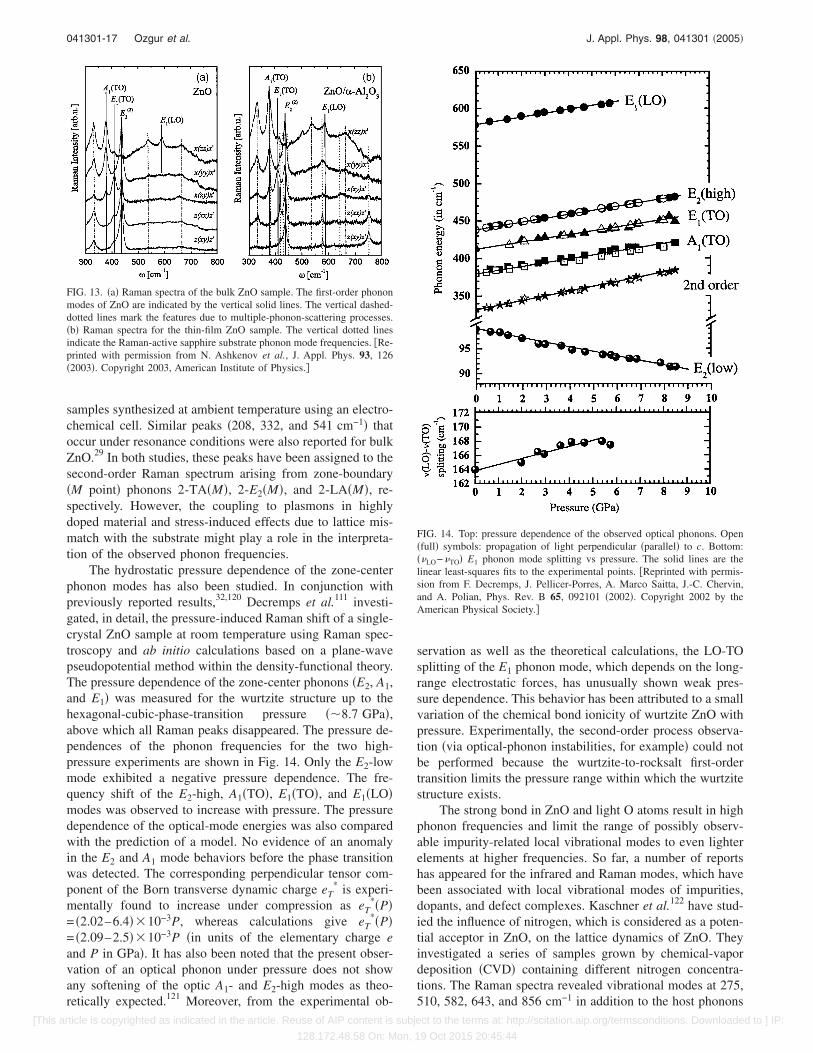
samples synthesized at ambient temperature using an electro-chemical cell. Similar peaks �208, 332, and 541 cm−1� thatoccur under resonance conditions were also reported for bulkZnO.29 In both studies, these peaks have been assigned to thesecond-order Raman spectrum arising from zone-boundary�M point� phonons 2-TA�M�, 2-E2�M�, and 2-LA�M�, re-spectively. However, the coupling to plasmons in highlydoped material and stress-induced effects due to lattice mis-match with the substrate might play a role in the interpreta-tion of the observed phonon frequencies.
The hydrostatic pressure dependence of the zone-centerphonon modes has also been studied. In conjunction withpreviously reported results,32,120 Decremps et al.111 investi-gated, in detail, the pressure-induced Raman shift of a single-crystal ZnO sample at room temperature using Raman spec-troscopy and ab initio calculations based on a plane-wavepseudopotential method within the density-functional theory.The pressure dependence of the zone-center phonons �E2, A1,and E1� was measured for the wurtzite structure up to thehexagonal-cubic-phase-transition pressure ��8.7 GPa�,above which all Raman peaks disappeared. The pressure de-pendences of the phonon frequencies for the two high-pressure experiments are shown in Fig. 14. Only the E2-lowmode exhibited a negative pressure dependence. The fre-quency shift of the E2-high, A1�TO�, E1�TO�, and E1�LO�modes was observed to increase with pressure. The pressuredependence of the optical-mode energies was also comparedwith the prediction of a model. No evidence of an anomalyin the E2 and A1 mode behaviors before the phase transitionwas detected. The corresponding perpendicular tensor com-ponent of the Born transverse dynamic charge eT
* is experi-mentally found to increase under compression as eT
*�P�= �2.02–6.4��10−3P, whereas calculations give eT
*�P�= �2.09–2.5��10−3P �in units of the elementary charge eand P in GPa�. It has also been noted that the present obser-vation of an optical phonon under pressure does not showany softening of the optic A1- and E2-high modes as theo-retically expected.121 Moreover, from the experimental ob-
servation as well as the theoretical calculations, the LO-TOsplitting of the E1 phonon mode, which depends on the long-range electrostatic forces, has unusually shown weak pres-sure dependence. This behavior has been attributed to a smallvariation of the chemical bond ionicity of wurtzite ZnO withpressure. Experimentally, the second-order process observa-tion �via optical-phonon instabilities, for example� could notbe performed because the wurtzite-to-rocksalt first-ordertransition limits the pressure range within which the wurtzitestructure exists.
The strong bond in ZnO and light O atoms result in highphonon frequencies and limit the range of possibly observ-able impurity-related local vibrational modes to even lighterelements at higher frequencies. So far, a number of reportshas appeared for the infrared and Raman modes, which havebeen associated with local vibrational modes of impurities,dopants, and defect complexes. Kaschner et al.122 have stud-ied the influence of nitrogen, which is considered as a poten-tial acceptor in ZnO, on the lattice dynamics of ZnO. Theyinvestigated a series of samples grown by chemical-vapordeposition �CVD� containing different nitrogen concentra-tions. The Raman spectra revealed vibrational modes at 275,510, 582, 643, and 856 cm−1 in addition to the host phonons
FIG. 13. �a� Raman spectra of the bulk ZnO sample. The first-order phononmodes of ZnO are indicated by the vertical solid lines. The vertical dashed-dotted lines mark the features due to multiple-phonon-scattering processes.�b� Raman spectra for the thin-film ZnO sample. The vertical dotted linesindicate the Raman-active sapphire substrate phonon mode frequencies. �Re-printed with permission from N. Ashkenov et al., J. Appl. Phys. 93, 126�2003�. Copyright 2003, American Institute of Physics.�
FIG. 14. Top: pressure dependence of the observed optical phonons. Open�full� symbols: propagation of light perpendicular �parallel� to c. Bottom:��LO−�TO� E1 phonon mode splitting vs pressure. The solid lines are thelinear least-squares fits to the experimental points. �Reprinted with permis-sion from F. Decremps, J. Pellicer-Porres, A. Marco Saitta, J.-C. Chervin,and A. Polian, Phys. Rev. B 65, 092101 �2002�. Copyright 2002 by theAmerican Physical Society.�
041301-17 Ozgur et al. J. Appl. Phys. 98, 041301 �2005�
[This article is copyrighted as indicated in the article. Reuse of AIP content is subject to the terms at: http://scitation.aip.org/termsconditions. Downloaded to ] IP:
128.172.48.58 On: Mon, 19 Oct 2015 20:45:44

of ZnO as discussed above. It has been observed that theintensity of these additional modes correlates linearly withthe nitrogen concentration. Therefore, these modes were in-terpreted as local vibrational modes due to the vibratingnitrogen-related complexes. The same group123 later mea-sured the phonon modes of Fe-, Sb-, Al-, Ga-, and Li-dopedZnO thin films, grown by pulsed-laser deposition on c-planesapphire substrates using polarized micro-Raman measure-ments. Additional modes at about 277, 511, 583, and644 cm−1, which had been assigned to N incorporation intheir previous work, were observed for intentionally dopedFe-, Sb-, and Al-doped films. The mode at 277 cm−1 was alsoobserved for Ga-doped films. Based on these observations ithas been stated that these modes cannot be related directly toN incorporation. Instead, they suggest intrinsic host latticedefects as their origin. Additional modes at 531, 631, and720 cm−1 were attributed to the Sb, Ga, and Fe dopants.
First-principles calculations based on DFT within theLDA and the pseudopotential-plane-wave method by Van deWalle124 suggest that hydrogen atoms might act as shallowdonors in ZnO. It was argued that the incorporation of hy-drogen accompanied by remarkably large relaxations of thesurrounding atoms lead to an O–H bond, which in fact, canbe regarded as a new type of dopant atom in ZnO. In order todetermine the microscopic structure of hydrogen donors, thelocal vibrational modes �LVMs� arising from these com-plexes have been investigated using IR and Ramanspectroscopies.125,126 The hydrogen-related defects in ZnOsamples, hydrogenated using a H or a D plasma, have beeninvestigated by a combination of local vibrational modespectroscopy and compared with the first-principles calcula-tions. Three new infrared �IR�-absorption lines at 3611.3,3349.6, and 3312.2 cm−1 have been observed at 10 K. Basedon polarization studies and first-principles calculations, theline at 3611.3 cm−1 was assigned to a single interstitial hy-drogen atom at the bond-center site oriented along the c axisof the crystal, although the possibility that this H atom isassociated with an impurity cannot be excluded. The lines at3349.6 and 3312.2 cm−1 were attributed to a zinc vacancythat contains two inequivalent hydrogen atoms, one in anO–H bond roughly aligned with the c axis, and the other inan O–H bond that forms an angle of 100° with the caxis.126,127
McCluskey et al.125 have also used IR spectroscopy tomeasure local vibrational modes in ZnO annealed in hydro-gen gas. An IR-absorption peak at 3326.3 cm−1 was observedat a temperature of 8 K and attributed to the O–H stretchmode based on comparison with the first-principles calcula-tions of Van de Walle,124 in which the calculated mode fre-quencies were 3726 and 3384 cm−1 for the bond-centeredand antibonding configurations, respectively, after subtract-ing 166 cm−1 due to the anharmonic terms in the potential,causing the stretch-mode frequency to shift downward. How-ever, because of the uncertainty in actual anharmonicity thebond-centered configuration was not ruled out. The IR spec-trum of ZnO annealed in deuterium has revealed an addi-tional stretch mode at 2470.3 cm−1 for the same temperature,which was tentatively assigned to the oxygen-deuterium�O–D� complexes. Using polarization measurements at room
temperature they also showed that the dipole of the O–Hcomplex does not lie parallel to the c axis of wurtziteZnO.128,129
More recently, using Raman-backscattering spectros-copy, Nickel and Fleischer130 have detected six local vibra-tional modes at 2854, 2890, 2918, 2948, 2988, and3096 cm−1. A Raman-backscattering spectrum measured onan as-grown ZnO single crystal is shown in Fig. 15. Thepeak positions were obtained by deconvoluting the spectruminto six Gaussian lines. In order to elucidate the origin of thelocal vibrational modes Nickel and Fleischer performed hy-drogen effusion experiments on ZnO single crystals. Uponannealing some samples up to 950 °C to remove hydrogenthe subsequent measurement revealed that the local vibra-tional modes disappeared, from which the observed vibra-tional modes are attributed to the presence of hydrogen in theZnO crystals. It has been found that the stretching vibrationof the corresponding hydrogen complex is not parallel to thec axis. The vibrational modes located at 2854, 2890, 2918,2948, and 2988 cm−1 were assumed to be due to the stretch-ing modes of C–H, symmetric stretching modes of C–H3,symmetric stretching modes of C–H2, antisymmetric stretch-ing modes of C–H3, and antisymmetric stretching modes ofC–H2, respectively, based on the effusion data, where a sig-nificant concentration of hydrocarbons were detected. Thelocal vibrational mode located at 3096 cm−1 was attributed tothe N–H, assuming a considerable amount of hydrogen isbonded to nitrogen atoms based on the effusion experimentaldata. This observed mode frequency was also found to beconsistent with that reported for ZnSe compoundsemiconductors.131
F. Thermal properties
1. Thermal-expansion coefficients
The lattice parameters of semiconductors are tempera-ture dependent and quantified by thermal-expansion coeffi-
FIG. 15. Raman-backscattering spectrum of as-grown single-crystal ZnOafter background subtraction. The sample was irradiated with the 488-nmline of an Ar laser and a power of 190 mW. The solid line represents aleast-squares fit of six Gaussian lines to the data. The dashed lines indicatethe individual local vibrational modes. The peak positions are indicated inthe plot. �Reprinted with permission from N. H. Nickel and K. Fleischer,Phys. Rev. Lett. 90, 197402 �2003�. Copyright 2003 by the American Physi-cal Society.�
041301-18 Ozgur et al. J. Appl. Phys. 98, 041301 �2005�
[This article is copyrighted as indicated in the article. Reuse of AIP content is subject to the terms at: http://scitation.aip.org/termsconditions. Downloaded to ] IP:
128.172.48.58 On: Mon, 19 Oct 2015 20:45:44

cients, which are defined as �a /a or �a and �c /c or �c, forin-and out-of-plane cases, respectively. They are dependenton stoichiometry, presence of extended defects, and free-carrier concentration. The temperature dependence of the lat-tice constants a and c, and the thermal-expansion coefficientsof hexagonal ZnO have been determined by the capacitivemethod.132 Reeber9 has employed x-ray powder-diffractionmethods to measure the temperature dependence of the lat-tice parameters of ZnO in the range of 4.2–296 K. The re-sults are shown in Fig. 16. When analyzing the dependenceof the lattice parameters on temperature, fourth-order poly-nomials,
aT = 3.248 53 − 1.0811 � 10−5T + 6.820 � 10−8T2
− 6.109 � 10−11T3 + 2.143 � 10−14T4, �8�
were fitted using the least-squares method, which gives aminimum for the a0 parameter at 93 K. The c0 parameter didnot give any minimum, most probably due to its less preci-sion and uncertainty in the measurement.
Han and Jou133 studied thermal properties of ZnO filmsprepared by rf magnetron sputtering on Si and GaAs sub-strates. Thermal stresses were determined by using the bend-ing beam technique where the specimens were thermallycycled from 25 to 400 °C. They investigated the thermal-expansion coefficient as a function of some growth param-eters, such as substrate temperature, sputtering power, etc.With a few exceptions, they found no significant changeswith the variation of total gas pressure from 0.53 to 2.1 Pa,substrate temperature from 250 to 450 °C, Ar-to-O pressureratio from 0.3 to 3, and power from 100 to 300 W. It hasbeen observed that the thermal-expansion coefficient in-creases about 37% from 5�10−6 to 8�10−6 1 / °C withinthe temperature range of 25–400 °C. Aoumeur et al.133 cal-culated the thermal-expansion coefficient for both the zinc-blende and rocksalt phases of ZnO using a molecular-dynamics simulation based on Tersoff’s potential. Theyfound that �=1.24�10−5 K−1 for the zinc-blende and �=0.16�10−5 K−1 for rocksalt structures.
2. Thermal conductivity
Thermal conductivity ���, which is a kinetic propertydetermined by the contributions from the vibrational, rota-tional, and electronic degrees of freedom, is an extremelyimportant material property when high-power/high-temperature electronic and optoelectronic devices are consid-ered. For pure crystals, phonon-phonon scattering, which isideally proportional to T−1 above the Debye temperature, isthe limiting process for thermal conductivity. The heat trans-port is predominantly determined by phonon-phonon um-klapp scattering, and phonon scattering by point and ex-tended defects, such as vacancies �inclusive of latticedistortions caused by them�, impurities, and isotope fluctua-tions �mass fluctuation�. As for other semiconductors, due totheir imperfection, point defects play a significant role in thethermal conductivity of ZnO. The lattice contribution �pho-non scattering� to the thermal conductivity � is obtainedfrom the kinetic theory as134
�lattice�T� =1
3�sClattice�T�L�T� , �9�
where T is the temperature, �s is the velocity of sound �al-most independent of temperature�, Clattice�T� is the latticespecific heat, and L�T� is the phonon mean free path. Inalmost all materials ��T� first increases with temperature,reaches a maximum ��max� at some characteristic tempera-ture Tch, and then decreases. At low temperatures L is rela-tively long and is dominated by extrinsic effects such as“defects” and/or finite crystal size and Clattice�T���T /D�3,where D is the Debye temperature. As the temperature in-creases Clattice�T� begins to saturate and intrinsictemperature-dependent umklapp processes become domi-nant, thus causing a decrease in L.
The electronic contribution to the thermal conductivitywhich is negligible for carrier concentrations �1019 cm−3
is135
�electr�T� =�2nkB
2T�electr
3mc* , �10�
where n is the carrier density, kB is the Boltzman constant,�electr is the scattering time of the electrons, and mc
* is theconduction-band effective mass. The overall thermal conduc-tivity generally decreases with increasing carrier concentra-tion, because the decrease in the lattice component of � dueto increased phonon scattering from both the impurities andfree electrons outweighs the increase in the electronic con-tribution to �.136
Scanning thermal microscopy �SThM� has been appliedto measure the room-temperature thermal conductivity on Znand O face of high-quality ZnO �0001� single crystals, grownby a vapor-phase transport method.137 The thermal investiga-tion was performed in two ways: point-by-point ��2-�mresolution� and area scans. The point-by-point measurementson Zn-face samples produced �=1.16±0.08 and1.02±0.07 W/cm K, while O-face samples showed �=1.10±0.09 and 0.98±0.08 W/cm K. The variations repre-sent the standard deviation in the data, which was obtainedby investigating approximately 15–20 points randomly dis-
FIG. 16. Wurtzite ZnO lattice parameters as a function of temperature.�Reprinted with permission from R. R. Reeber, J. Appl. Phys. 41, 5063�1970�. Copyright 1970, American Institute of Physics.�
041301-19 Ozgur et al. J. Appl. Phys. 98, 041301 �2005�
[This article is copyrighted as indicated in the article. Reuse of AIP content is subject to the terms at: http://scitation.aip.org/termsconditions. Downloaded to ] IP:
128.172.48.58 On: Mon, 19 Oct 2015 20:45:44

tributed over a 6�6-mm2 surface area. In this study, a cor-relation between the surface topography and thermal-conductivity variations was also studied by acquiring theAFM and SThM scans simultaneously during the area scan.The effects of surface roughness on effective � values weretreated in terms of tip-surface geometry. It was argued thatwhen the experimental voltage variations �proportional to ��correspond to only 6%–7% changes in the thermal conduc-tivity, variations probably originate from the topography.Larger variations ��12% � in the SThM voltage reading forAFM topographical features with heights �100 nm wouldbe an indication of intrinsic thermal-conductivity variationsacross the area under investigation.
Pollak et al.138 measured the thermal conductivity � ofseveral bulk ZnO �0001� samples grown by CERMET, Inc.,and prepared by our group under different surface treat-ments. The measurements were made using SThM with aspatial/depth resolution of about 2–3 �m. The surface treat-ments of various samples are summarized in Table VI. Themeasurements were made at different points on each sampleand the results are also shown in Table VI. On sample a inboth positions, � is considerably less than the previouslyreported values of about 1.0 W/cm K.137 To be consistentwith the earlier models, one would argue that forming-gasannealing has resulted in surface roughness, which has con-siderably reduced �. The same is mostly true for sample e,which exhibits considerable inhomogeneity in the measured�. At the present time we do not have an explanation for thisresult, although Florescu et al.136 did find that in GaN, � wasa function of carrier concentration, i.e., it decreased withincreasing carrier concentration due to scattering of phononsfrom the ionized impurities. We have no information aboutthe carrier concentrations/doping levels, nor their distributionfor this or any other of the samples. For sample b the mea-sured results for � are similar to those reported in Ref. 137,while for samples c and d they are actually somewhat higherand are the highest � values reported for ZnO. Thus, air-annealing and nitrogen-plasma treatment both result in agood surface.
Olorunyolemi et al.139 measured the thermal conductiv-ity of ZnO powders with different particle sizes �micrometer,submicrometer, and nanometer� from the as-received powderstate to the fully sintered state using a laser flash technique.Curves of thermal conductivity versus temperature for thethree sets of ZnO samples �micrometer, submicrometer, andnanometer�, measured as they were heated to 600 °C andcooled back to 25 °C, are shown in Fig. 17. The first surpris-ing observation is that the thermal conductivity at room tem-perature and up to 200 °C is the reverse of what is expectedfor the different particle sizes, with the nanopowder havingthe highest thermal conductivity. The room-temperature ther-mal conductivities were measured as 0.745, 0.914, and1.160 W/m K for micro-, submicro-, and nanosize sampleshaving average particle diameters of 1.0 �m, 0.2 �m, and20 nm, respectively. The initial higher thermal conductivityof the nanopowder ZnO samples were attributed to the ad-sorbed water including chemisorbed water �more than thatadsorbed by the submicrometer, which in turn is more thanthat adsorbed by the micrometer powder�. Above 400 °C thethermal conductivity of the nanoparticle size increases fasterwith increasing temperature than that of the submicrometerand the micrometer particle size samples. In this work, amodel for interparticle neck growth was also developedbased on mass transfer to the neck region of a powder as aresult of a known temperature. The observed data were com-pared with the theoretical results obtained by the three-dimensional numerical code combined with this model.
Figure 18 shows the measured thermal conductivity of afully sintered sample heated from room temperature to1000 °C. The thermal conductivity decreases from37 to 4 W/m K as the temperature is increased from roomtemperature to 1000 °C. This is the thermal conductivitycurve for a fully dense ZnO crystal, where the resistivephonon-phonon interactions �umklapp processes� are thedominant scattering mechanism.
The thermal properties of ZnO doped with Al and Mgwere also studied by a number of groups140–144 for the evalu-ation of the thermoelectric performance. Tsubota et al.143 in-
TABLE VI. Thermal conductivity, � �W/cm K�, at multiple positions ofbulk ZnO samples with various surface treatments �Ref. 138�.
Sample Surface treatmentThermal conductivity
�W/cm K�
a Forming-gas-annealed �1� �=0.67±0.08�2� �=0.46±0.05
b As-received �O face� �1� �=1.00±0.08�2� �=0.95±0.06
c Air-annealed �1� �=1.35±0.08�2� �=1.25±0.05
d Nitrogen plasma treated at 750 °C �1� �=1.44±0.08�2� �=1.47±0.08
e Oxygen plasma treated at 700 °C �1� �=0.87±0.06�2� �=0.75±0.06�3� �=0.80±0.06�4� �=1.24±0.05�5� �=0.54±0.07
FIG. 17. Thermal conductivity of nanometer, submicrometer, and microme-ter particle size ZnO heated from room temperature to 600 °C at 3 °C/min.�Reprinted with permission from T. Olorunyolemi, A. Birnboim, Y. Carmel,O. C. Wilson, Jr., and I. K. Lloyd, J. Am. Ceram. Soc. 85, 1249 �2002�.Copyright 2002, Blackwell Publishing.�
041301-20 Ozgur et al. J. Appl. Phys. 98, 041301 �2005�
[This article is copyrighted as indicated in the article. Reuse of AIP content is subject to the terms at: http://scitation.aip.org/termsconditions. Downloaded to ] IP:
128.172.48.58 On: Mon, 19 Oct 2015 20:45:44

vestigated the thermal conductivity of sintered�Zn1−yMgy�1−xAlxO �x=0–0.1 and y=0–0.1� samples deter-mined from thermal diffusivity and specific-heat capacitymeasured by the laser flash technique and differential scan-ning calorimetry �DSC�, respectively. The temperature de-pendences of the thermal conductivities of�Zn1−yMgy�0.98Al0.02O �y=0,0.02,0.1� are shown in Fig. 19in comparison with that of ZnO. The reduction of � fromZnO to Zn0.98Al0.02O was almost negligible. Although addi-tion of Al �using Al2O3� is considered to be ineffective insuppressing � of ZnO-based materials, the difference in the �values between the MgO-added samples and theZn0.98Al0.02O sample is significantly larger at low tempera-tures, indicating that the addition of MgO was very effectivein reducing the thermal conductivity at low temperatures.From the temperature-dependence behavior �1/T dependenceabove the Debye temperature� the authors have concludedthat the decrease in phonon-phonon-scattering contribution ismainly responsible for the reduction of thermal conductivityupon addition of MgO as well as Al2O3. Formation of a solidsolution of MgO and ZnO is thereby considered to be effec-tive in introducing phonon-scattering centers in order to re-duce the vibrational component, and thereby the overallvalue of �.
Similarly, thermal properties of �Zn1−yMgy�1−xAlxO �0�x�0.05 and 0�y�0.16� ceramics synthesized from apowder precursor prepared by a polymerized complexmethod has also been investigated by Katsuyama et al.142
They observed similar dependence of thermal conductivityon temperature and doping constitutes as Tsubota et al.143
The thermal conductivity decreased with increasing x, butfurther suppression of the thermal conductivity was attainedby the additional substitution of the Zn sites by Mg atomswith the resultant lattice contribution, i.e., the point defectsintroduced by the addition of Mg enhanced the phonon scat-tering. However, in both studies, although the temperaturedependence reveals 1 /T behavior indicative of umklapp scat-tering, room-temperature thermal conductivity of sinteredZnO, which is about 40 W m−1 K−1 and reduces to�7 W m−1 K−1 with increasing MgO concentration, is muchsmaller than the values reported for the high-quality singlecrystal discussed above. This indicates the large contributiondue to enhanced phonon-point defects or –extended defectsand grain-boundary scattering.
3. Specific heat
The specific heat of a semiconductor has contributionsfrom lattice vibrations, free carriers �very effective at lowtemperatures�, and point and extended defects. For good-quality semi-insulating crystal, the specific heat is deter-mined mostly by the lattice vibrations. The availablespecific-heat data for ZnO are very limited. Only Lawlessand Gupta145 investigated the specific heat for both pure andvaristor types of ZnO samples between the temperatureranges of 1.7 and 25 K, where the latter has an average grainsize of 10 �m. Specific-heat measurements were performedusing the pulse method. As seen in Fig. 20, the specific heatof varistor ZnO diverges from that of pure ZnO below 20 K.This difference was attributed to the contribution by the large
FIG. 18. Thermal conductivity of fully sintered ZnO heated from roomtemperature to 1000 °C. �Reprinted with permission from T. Olorunyolemi,A. Birnboim, Y. Carmel, O. C. Wilson, Jr., and I. K. Lloyd, J. Am. Ceram.Soc. 85, 1249 �2002�. Copyright 2002, Blackwell Publishing.�
FIG. 19. The thermal conductivities of ZnO ���, Zn0.98Al0.02O ���, and�Zn1−yMgy�0.98Al0.02O for y=0.02 ��� and 0.1 ��� as a function of inversetemperature. �Reproduced by permission of the Royal Society of Chemistryfrom T. Tsubota, M. Ohtaki, K. Eguchi, and H. Arai, J. Mater. Chem. 8, 409�1998�.�
FIG. 20. Specific-heat data measured for pure ZnO compared to the data forvaristor ZnO. �Reprinted with permission from W. N. Lawless and T. K.Gupta, J. Appl. Phys. 60, 607 �1986�. Copyright 1986, American Institute ofPhysics.�
041301-21 Ozgur et al. J. Appl. Phys. 98, 041301 �2005�
[This article is copyrighted as indicated in the article. Reuse of AIP content is subject to the terms at: http://scitation.aip.org/termsconditions. Downloaded to ] IP:
128.172.48.58 On: Mon, 19 Oct 2015 20:45:44

amount of impurities present in the region of the grainboundaries of varistor-type ZnO, giving rise to a very largeexcess specific heat below 20 K.
The specific-heat data for pure ZnO were further ana-lyzed by considering two non-Debye features at differenttemperature regions according to
C = CDebye + CSchottky + CEinstein, �11�
where CDebye, CSchottky, and CEinstein represent the Debye,Schottky, and Einstein terms of the total specific heat ofZnO, respectively. In general, the Debye expression for thetemperature dependence of specific heat in a solid at a con-stant pressure can be expressed as
CDebye = 18R T
D3�
0
xD x4ex
�ex − 1�2dx , �12�
where xD�D /T, and R=8.3144 J /mol K is the molar gasconstant. The coefficient in front of the term R has beenmultiplied by 2 to take into account the two constituentsmaking up the binary compound. By fitting the measuredtemperature-dependent heat capacity to the Debye expres-sion, one can obtain the Debye temperature D specific to theheat capacity. It is often easier to extract a Debye tempera-ture using data either near very low temperatures or wellbelow the Debye temperature where the specific heat has asimple cubic dependence on temperature:
CDebye = 234R T
D3
. �13�
Unfortunately for ZnO, the samples contain large densities offree carriers and defects, which make the Debye specific-heatexpression unreliable. The Debye contribution to the specificheat of pure ZnO is also shown in Fig. 20 as the curvelabeled with a calorimetric Debye temperature of D
=399.5 K, and the deviation of the data below �5 K is dueto the Schottky term, and above �10 K due to the Einsteinterm. The latter has an exponential dependence and is givenby
CEinstein = 3RrEE
T2
exp−E
T for T � E, �14�
where rE is the number of Einstein oscillators per formulaweight and E is the Einstein temperature. The Schottky termhas a T−2 dependence and is expressed by
CSchottky = bT−2, �15�
where b=nR�� /2�2 �n=rE is assumed� is the Schottky coef-ficient.
The least-squares fit of these two expressions to the ex-perimental data for the corresponding temperature range isshown in Fig. 21. Very good agreement with 2%–3% uncer-tainty was achieved for the values of E=120.5 K and rE
=8.72�10−2 for the case of the Einstein model, and b=350.7 ergs g−1 K−1 for the Schottky term. The Zn intersti-tials �3.6�1021 cm−3� might be responsible for the disper-sionless Einstein-type contribution to the specific heat above10 K, whereas the Schottky contribution appearing below
4 K is due to ordering of, possibly, Zn interstitials with acharacteristic energy of �=1.1�105 eV for such an orderingmechanism.
G. Electrical properties of undoped ZnO
As a direct and large-band-gap material, ZnO is attract-ing a lot of attention for a variety of electronic and optoelec-tronic applications. Advantages associated with a large bandgap include higher breakdown voltages, ability to sustainlarge electric fields, lower noise generation, and high-temperature and high-power operation. The electron trans-port in semiconductors can be considered for low and highelectric fields. �i� At sufficiently low electric fields, the en-ergy gained by the electrons from the applied electric field issmall compared to the thermal energy of electrons, and there-fore, the energy distribution of electrons is unaffected bysuch a low electric field. Since the scattering rates determin-ing the electron mobility depend on the electron distributionfunction, electron mobility remains independent of the ap-plied electric field, and Ohm’s law is obeyed. �ii� When theelectric field is increased to a point where the energy gainedby electrons from the external field is no longer negligiblecompared to the thermal energy of the electron, the electrondistribution function changes significantly from its equilib-rium value. These electrons become hot electrons character-ized by an electron temperature larger than the lattice tem-perature. Furthermore, as the dimensions of the device are
FIG. 21. Fit to the pure ZnO data �a� using the Schottky model �this fityields a Debye temperature of 395.5 K� and �b� using the Einstein model.Cex is obtained by removing the Debye and Schottky contributions. TheEinstein oscillators are identified as the Zn interstitials. �Reprinted withpermission from W. N. Lawless and T. K. Gupta, J. Appl. Phys. 60, 607�1986�. Copyright 1986, American Institute of Physics.�
041301-22 Ozgur et al. J. Appl. Phys. 98, 041301 �2005�
[This article is copyrighted as indicated in the article. Reuse of AIP content is subject to the terms at: http://scitation.aip.org/termsconditions. Downloaded to ] IP:
128.172.48.58 On: Mon, 19 Oct 2015 20:45:44

decreased to submicron range, transient transport occurswhen there is minimal or no energy loss to the lattice duringa short and critical period of time, such as during transportunder the gate of a field-effect transistor or through the baseof a bipolar transistor. The transient transport is characterizedby the onset of ballistic or velocity overshoot phenomenon.Since the electron drift velocity is higher than its steady-statevalue, one can design a device operating at frequencies ex-ceeding those expected from linear scaling of dimensions.
1. Low-field transport
Hall effect is the most widely used technique to measurethe transport properties and assess the quality of epitaxiallayers. For semiconductor materials, it yields the carrier con-centration, its type, and carrier mobility. More specifically,experimental data on Hall measurements over a wide tem-perature range �4.2–300 K� provide quantitative informationon impurities, imperfections, uniformity, scattering mecha-nisms, etc. The Hall coefficient and resistivity ��� are experi-mentally determined and then related to the electrical param-eters through �for n-type conduction� RH=rH /ne and �H
=RH /�, where n is the free-electron concentration, e is theunit electronic charge, �H is the Hall mobility, and rH is theHall scattering factor which is dependent on the particularscattering mechanism. The drift mobility is the average ve-locity per unit electric field in the limit of zero electric fieldand is related to the Hall mobility through the Hall scatteringfactor by �H=rH�. As noted above, the Hall scattering factordepends on the details of the scattering mechanism, whichlimits the drift velocity. As the carriers travel through a semi-conductor, they encounter various scattering mechanismsthat govern the carrier mobility in the electronic system. Theparameter for characterizing the various scattering mecha-nisms is the relaxation time �, which determines the rate ofchange in electron momentum as it moves in the semicon-ductor crystal. Mobility is related to the scattering time by
� =q���m* , �16�
where m* is the electron effective mass, q is the electroniccharge, and ��� is the relaxation time averaged over the en-ergy distribution of electrons. The total relaxation time �T
when various scattering mechanisms are operative is givenby Matthiessen’s rule:
1
�T= �
i
1
�i, �17�
where i represents each scattering process, provided that theelectron while undergoing one scattering event is not af-fected by another.
The major scattering mechanisms that generally governthe electron transport in III-V semiconductors are also validfor ZnO. They are briefly listed as follows.
�1� Ionized impurity scattering is due to deflection of freecarriers by the long-range Coulomb potential of thecharged centers caused by defects or intentionally doped
impurities. This can be thought as a local perturbation ofthe band edge, which affects the electron motion.
�2� Polar LO-phonon scattering is caused by the interactionof a moving charge with an electric field induced byelectric polarization associated with lattice vibration dueto the ionic nature of the bonds in a polar semiconductor.
�3� Acoustic-phonon scattering through deformation poten-tial arises from the energy change of the band edgesinduced by strain associated with acoustic phonons,where the scattering rate increases with the wave vectorsof the phonons.
�4� Piezoelectric scattering arises from the electric fieldsthat are produced by the strain associated with phononsin a crystal without inversion symmetry.
�5� If the density of dislocations and native defects are highin a semiconductor, dislocation scattering and scatteringthrough defects are also considered as possible scatter-ing mechanisms. Dislocation scattering is due to the factthat acceptor centers are introduced along the dislocationline, which capture electrons from the conduction bandin an n-type semiconductor. The dislocation lines be-come negatively charged and a space-charge region isformed around it, which scatters electrons travelingacross the dislocations, thus reducing the mobility.
Experimental investigation of the temperature-dependentcarrier mobility and concentration can be used to determinethe fundamental material parameters and understand the car-rier scattering mechanisms along with an accurate compari-son with theory. Table VII gives the selected best values ofelectron mobility and corresponding carrier concentration inbulk and thin-film ZnO grown by various techniques.
The transport properties reported in the literature aremostly based on Hall-effect measurements, assuming theHall scattering factor to be unity. Using Monte Carlo simu-lations, Albrecht et al.146 predicted the room-temperatureelectron mobility of ZnO as �300 cm2/V s. Nominally un-doped ZnO with a wurtzite structure naturally becomes ann-type semiconductor due to the presence of intrinsic or ex-trinsic defects, which were generally attributed to native de-fects, such as the Zn-on-O antisite �ZnO�, the Zn interstitial�ZnI�, and the O vacancy �VO�.146 However, recently first-principles investigations based on density-functional theorysuggest that hydrogen in ZnO occurs exclusively in the posi-tive charge state and is responsible for the n-type conductiv-ity of ZnO �Ref. 124� �discussed in detail in Sec. V�. Thehighest room-temperature electron mobility for a bulk ZnOsingle crystal grown by vapor-phase transport method is re-ported to be about 205 cm2/V s with a carrier concentrationof 6.0�1016 cm−3.146 This value is very close to the pre-dicted mobility value. The Hall data obtained as a function oftemperature is shown in Fig. 22. The mobility data werefitted using Rode’s method of solving the Boltzmann trans-port equation by taking into consideration the major scatter-ing mechanisms, such as polar-optical-phonon scattering,acoustic-phonon scattering through deformation and piezo-electric potentials, and Coulomb scattering from ionized im-purities or defects. It was argued that the conduction wasdominated by hopping at 8 K due to the carrier freeze-out
041301-23 Ozgur et al. J. Appl. Phys. 98, 041301 �2005�
[This article is copyrighted as indicated in the article. Reuse of AIP content is subject to the terms at: http://scitation.aip.org/termsconditions. Downloaded to ] IP:
128.172.48.58 On: Mon, 19 Oct 2015 20:45:44
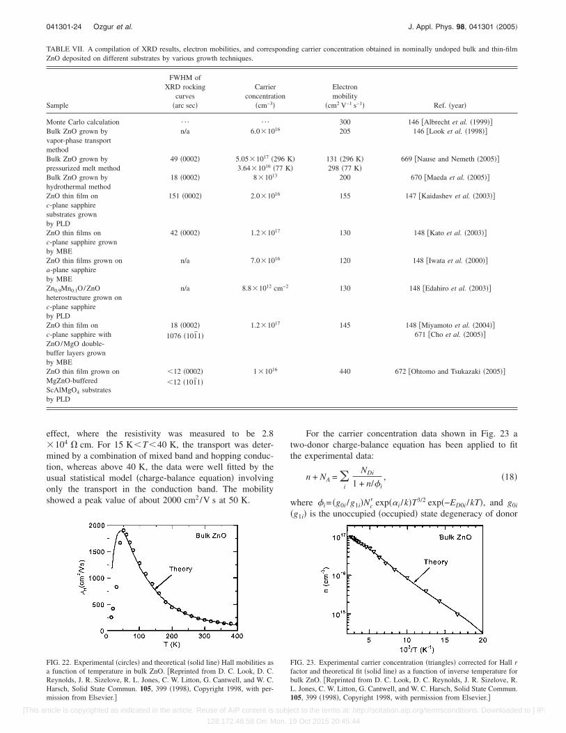
effect, where the resistivity was measured to be 2.8�104 � cm. For 15 K�T�40 K, the transport was deter-mined by a combination of mixed band and hopping conduc-tion, whereas above 40 K, the data were well fitted by theusual statistical model �charge-balance equation� involvingonly the transport in the conduction band. The mobilityshowed a peak value of about 2000 cm2/V s at 50 K.
For the carrier concentration data shown in Fig. 23 atwo-donor charge-balance equation has been applied to fitthe experimental data:
n + NA = �i
NDi
1 + n/�i, �18�
where �i= �g0i /g1i�Nc� exp��i /k�T3/2 exp�−ED0i /kT�, and g0i
�g1i� is the unoccupied �occupied� state degeneracy of donor
TABLE VII. A compilation of XRD results, electron mobilities, and corresponding carrier concentration obtained in nominally undoped bulk and thin-filmZnO deposited on different substrates by various growth techniques.
Sample
FWHM ofXRD rocking
curves�arc sec�
Carrierconcentration
�cm−3�
Electronmobility
�cm2 V−1 s−1� Ref. �year�
Monte Carlo calculation ¯ ¯ 300 146 �Albrecht et al. �1999��Bulk ZnO grown byvapor-phase transportmethod
n/a 6.0�1016 205 146 �Look et al. �1998��
Bulk ZnO grown bypressurized melt method
49 �0002� 5.05�1017 �296 K�3.64�1016 �77 K�
131 �296 K�298 �77 K�
669 �Nause and Nemeth �2005��
Bulk ZnO grown byhydrothermal method
18 �0002� 8�1013 200 670 �Maeda et al. �2005��
ZnO thin film onc-plane sapphiresubstrates grownby PLD
151 �0002� 2.0�1016 155 147 �Kaidashev et al. �2003��
ZnO thin films onc-plane sapphire grownby MBE
42 �0002� 1.2�1017 130 148 �Kato et al. �2003��
ZnO thin films grown ona-plane sapphireby MBE
n/a 7.0�1016 120 148 �Iwata et al. �2000��
Zn0.9Mn0.1O/ZnOheterostructure grown onc-plane sapphireby PLD
n/a 8.8�1012 cm−2 130 148 �Edahiro et al. �2003��
ZnO thin film onc-plane sapphire withZnO/MgO double-buffer layers grownby MBE
18 �0002�1076 �101̄1�
1.2�1017 145 148 �Miyamoto et al. �2004��671 �Cho et al. �2005��
ZnO thin film grown onMgZnO-bufferedScAlMgO4 substratesby PLD
�12 �0002��12 �101̄1�
1�1016 440 672 �Ohtomo and Tsukazaki �2005��
FIG. 22. Experimental �circles� and theoretical �solid line� Hall mobilities asa function of temperature in bulk ZnO. �Reprinted from D. C. Look, D. C.Reynolds, J. R. Sizelove, R. L. Jones, C. W. Litton, G. Cantwell, and W. C.Harsch, Solid State Commun. 105, 399 �1998�, Copyright 1998, with per-mission from Elsevier.�
FIG. 23. Experimental carrier concentration �triangles� corrected for Hall rfactor and theoretical fit �solid line� as a function of inverse temperature forbulk ZnO. �Reprinted from D. C. Look, D. C. Reynolds, J. R. Sizelove, R.L. Jones, C. W. Litton, G. Cantwell, and W. C. Harsch, Solid State Commun.105, 399 �1998�, Copyright 1998, with permission from Elsevier.�
041301-24 Ozgur et al. J. Appl. Phys. 98, 041301 �2005�
[This article is copyrighted as indicated in the article. Reuse of AIP content is subject to the terms at: http://scitation.aip.org/termsconditions. Downloaded to ] IP:
128.172.48.58 On: Mon, 19 Oct 2015 20:45:44

i. The term Nc� is the effective conduction-band density ofstates at T=1 K and �i is the temperature coefficient definedby EDi=ED0i−�iT, where EDi is the activation energy of do-nor i. Although their origin was left unclear in this work ithas been determined that the dominant hydrogenic shallowdonor had a concentration of about 1�1017 cm−3 and anenergy of about 60 meV, whereas the total acceptor concen-tration was much lower, about 2�1015 cm−3, resulting in alower compensation ratio of 0.02. However, the shallowerdonor that was ruled out in this work due to its smallerconcentration �about one order of magnitude less than thedeeper donor� at an energy of �31 meV was further inves-tigated later by the same group.146 They reported that high-energy electron irradiation in ZnO produces shallow donorsat about 30 meV. Because the process was found to be po-larity dependent, where the production rate is much higher
for Zn-face �0001� than O-face �0001̄� irradiation, it has beenconcluded that this native shallower donor is related to aZn-sublattice defect, most likely the interstitial ZnI or aZnI-related complex.
Regarding the ZnO epilayers grown by various growthtechniques on different substrates, room-temperature mobili-ties are relatively poor147 �typically below 100 cm2/V s�compared to bulk ZnO, particularly the variety grown by thevapor-transport method. However, as listed in Table VIIsome room-temperature mobility values are comparable tothe best reported value for bulk ZnO. Kaidashev et al.147
reported the best reproducible electron mobilities from 115up to 155 cm2/V s at 300 K in a narrow carrier concentra-tion range from 2�1016 to 5�1016 cm−3 for nominally un-doped ZnO thin films of total thickness of 1–2 �m grown onc-plane sapphire substrates by a multistep PLD technique.They attributed this success to the multistep PLD process,which includes the insertion of 30-nm-thin ZnO relaxationlayers deposited at a reduced substrate temperature. The to-pographical properties of the films were correlated with thecorresponding electrical properties. The high-mobilitysamples showed atomically flat surface structure with a grainsize of about 0.5–1 �m, whereas the surfaces of low-mobility films consist of clearly resolved hexagonally fac-eted columnar grains of only 200-nm size. The observationof the excitonic features at low-temperature photolumines-cence spectra also reflects the quality of the samples, whichis of primary importance to improve the electrical propertiesof ZnO.
Kato et al. and Iwata et al.148 have performed similarand successful studies on heteroepitaxially grown ZnO epil-ayers using plasma-assisted molecular-beam epitaxy �MBE�and radical-source MBE techniques. Kato et al.148 used
�112̄0� a-plane sapphire substrates and high-temperaturegrowth with low-temperature buffer layers for high-qualityundoped ZnO epitaxial films. They obtained electron mobili-ties as high as 120 cm2/V s and residual carrier concentra-tions as low as 7�1016 cm−3. With further optimization ofthe growth condition such as O/Zn flux ratio, a maximummobility of 130 cm2/V s with a residual carrier concentra-tion of 1.2�1017 cm−3 was reported.148 It has been sug-gested that stoichiometric ZnO films have the lowest dislo-
cation density and the highest electron mobility compared toZnO films grown under nonstoichiometric flux conditions.Iwata et al.148 used ZnO/MgO double-buffer layers for high-electron-mobility ZnO epilayers grown on c-plane sapphire.It has been argued that the precisely controlled low growthrate of the double-buffer layers was crucial for the improve-ment of electrical properties. The highest electron mobilityof 145 cm2/V s in MBE-grown ZnO film was reported atroom temperature. This improvement was attributed to a de-crease in dislocation density, based on both x-ray-diffraction�-rocking curve measurements and calculated electron mo-bilities.
ZnO-based heterostructures, which contain magnetic im-purities in the barrier layer, were grown on c-cut sapphiresubstrates by pulsed-laser deposition by Edahiro et al.148 Thetemperature dependence of the mobility of theZn0.9Mn0.1O/ZnO heterostructure exhibits the suppression ofionized impurity scattering below 100 K as shown in Fig. 24.The carrier concentration and the mobility measured at1.85 K are 4.0�1012 cm−2 and 360 cm2/V s, respectively.These transport properties revealed that two-dimensionalelectron gas is successfully formed at the Zn0.9Mn0.1O/ZnOinterface.
2. High-field transport
Ensemble Monte Carlo �MC� simulations have been thepopular tools to investigate the steady-state electron transportin semiconductors theoretically. In particular, the steady-statevelocity-field characteristics have been determined using theMonte Carlo method for electric-field strengths up to350 kV/cm in bulk, wurtzite-structure ZnO at lattice tem-peratures of 300, 450, and 600 K.146 The conduction bandsof wurtzite-phase ZnO structure were calculated using FP-LMTO-LDA method. For the MC transport simulation, thelowest � valley ��1 symmetry� and the satellite valleys lo-cated at � ��3 symmetry� and at U point, Umin �U1 symme-try�, which is located two-thirds of the way between the Mand L symmetry points on the edge of the Brillouin zone,were considered.
The calculated electron drift velocity versus electric-fieldcharacteristics are plotted in Fig. 25 for wurtzite-phase ZnO
FIG. 24. Temperature dependence of the mobility of the ZnMnO/ZnO het-erostructure �squares� and the 1-�m-thick ZnO single-layer �triangles� con-trol sample. �Reprinted with permission from T. Edahiro, N. Fujimura, andT. Ito, J. Appl. Phys. 93, 7673 �2003�. Copyright 2003, American Institute ofPhysics.�
041301-25 Ozgur et al. J. Appl. Phys. 98, 041301 �2005�
[This article is copyrighted as indicated in the article. Reuse of AIP content is subject to the terms at: http://scitation.aip.org/termsconditions. Downloaded to ] IP:
128.172.48.58 On: Mon, 19 Oct 2015 20:45:44
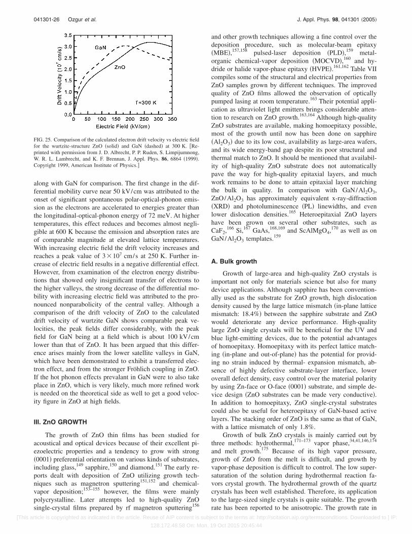
along with GaN for comparison. The first change in the dif-ferential mobility curve near 50 kV/cm was attributed to theonset of significant spontaneous polar-optical-phonon emis-sion as the electrons are accelerated to energies greater thanthe longitudinal-optical-phonon energy of 72 meV. At highertemperatures, this effect reduces and becomes almost negli-gible at 600 K because the emission and absorption rates areof comparable magnitude at elevated lattice temperatures.With increasing electric field the drift velocity increases andreaches a peak value of 3�107 cm/s at 250 K. Further in-crease of electric field results in a negative differential effect.However, from examination of the electron energy distribu-tions that showed only insignificant transfer of electrons tothe higher valleys, the strong decrease of the differential mo-bility with increasing electric field was attributed to the pro-nounced nonparabolicity of the central valley. Although acomparison of the drift velocity of ZnO to the calculateddrift velocity of wurtzite GaN shows comparable peak ve-locities, the peak fields differ considerably, with the peakfield for GaN being at a field which is about 100 kV/cmlower than that of ZnO. It has been argued that this differ-ence arises mainly from the lower satellite valleys in GaN,which have been demonstrated to exhibit a transferred elec-tron effect, and from the stronger Fröhlich coupling in ZnO.If the hot phonon effects prevalant in GaN were to also takeplace in ZnO, which is very likely, much more refined workis needed on the theoretical side as well to get a good veloc-ity figure in ZnO at high fields.
III. ZnO GROWTH
The growth of ZnO thin films has been studied foracoustical and optical devices because of their excellent pi-ezoelectric properties and a tendency to grow with strong�0001� preferential orientation on various kinds of substrates,including glass,149 sapphire,150 and diamond.151 The early re-ports dealt with deposition of ZnO utilizing growth tech-niques such as magnetron sputtering151,152 and chemical-vapor deposition;153–155 however, the films were mainlypolycrystalline. Later attempts led to high-quality ZnOsingle-crystal films prepared by rf magnetron sputtering156
and other growth techniques allowing a fine control over thedeposition procedure, such as molecular-beam epitaxy�MBE�,157,158 pulsed-laser deposition �PLD�,159 metal-organic chemical-vapor deposition �MOCVD�,160 and hy-dride or halide vapor-phase epitaxy �HVPE�.161,162 Table VIIcompiles some of the structural and electrical properties fromZnO samples grown by different techniques. The improvedquality of ZnO films allowed the observation of opticallypumped lasing at room temperature.163 Their potential appli-cation as ultraviolet light emitters brings considerable atten-tion to research on ZnO growth.163,164 Although high-qualityZnO substrates are available, making homoepitaxy possible,most of the growth until now has been done on sapphire�Al2O3� due to its low cost, availability as large-area wafers,and its wide energy-band gap despite its poor structural andthermal match to ZnO. It should be mentioned that availabil-ity of high-quality ZnO substrate does not automaticallypave the way for high-quality epitaxial layers, and muchwork remains to be done to attain epitaxial layer matchingthe bulk in quality. In comparison with GaN/Al2O3,ZnO/Al2O3 has approximately equivalent x-ray-diffraction�XRD� and photoluminescence �PL� linewidths, and evenlower dislocation densities.165 Heteroepitaxial ZnO layershave been grown on several other substrates, such asCaF2,166 Si,167 GaAs,168,169 and ScAlMgO4,170 as well as onGaN/Al2O3 templates.159
A. Bulk growth
Growth of large-area and high-quality ZnO crystals isimportant not only for materials science but also for manydevice applications. Although sapphire has been convention-ally used as the substrate for ZnO growth, high dislocationdensity caused by the large lattice mismatch �in-plane latticemismatch: 18.4%� between the sapphire substrate and ZnOwould deteriorate any device performance. High-qualitylarge ZnO single crystals will be beneficial for the UV andblue light-emitting devices, due to the potential advantagesof homoepitaxy. Homoepitaxy with its perfect lattice match-ing �in-plane and out-of-plane� has the potential for provid-ing no strain induced by thermal- expansion mismatch, ab-sence of highly defective substrate-layer interface, loweroverall defect density, easy control over the material polarityby using Zn-face or O-face �0001� substrate, and simple de-vice design �ZnO substrates can be made very conductive�.In addition to homoepitaxy, ZnO single-crystal substratescould also be useful for heteroepitaxy of GaN-based activelayers. The stacking order of ZnO is the same as that of GaN,with a lattice mismatch of only 1.8%.
Growth of bulk ZnO crystals is mainly carried out bythree methods: hydrothermal,171–173 vapor phase,34,41,146,174
and melt growth.175 Because of its high vapor pressure,growth of ZnO from the melt is difficult, and growth byvapor-phase deposition is difficult to control. The low super-saturation of the solution during hydrothermal reaction fa-vors crystal growth. The hydrothermal growth of the quartzcrystals has been well established. Therefore, its applicationto the large-sized single crystals is quite suitable. The growthrate has been reported to be anisotropic. The growth rate in
FIG. 25. Comparison of the calculated electron drift velocity vs electric fieldfor the wurtzite-structure ZnO �solid� and GaN �dashed� at 300 K. �Re-printed with permission from J. D. Albrecht, P. P. Ruden, S. Limpijumnong,W. R. L. Lambrecht, and K. F. Brennan, J. Appl. Phys. 86, 6864 �1999�.Copyright 1999, American Institute of Physics.�
041301-26 Ozgur et al. J. Appl. Phys. 98, 041301 �2005�
[This article is copyrighted as indicated in the article. Reuse of AIP content is subject to the terms at: http://scitation.aip.org/termsconditions. Downloaded to ] IP:
128.172.48.58 On: Mon, 19 Oct 2015 20:45:44

the �0001� direction was �0.25 mm/day, and the ratio ofgrowth rates between the fast ��0001�� direction and slow
��0001̄�� direction was 3:1.176 However, the hydrothermalcrystals inevitably incorporate alkali metals �K and Li� andsmall amounts of metallic impurities from the solution.
Figure 26 shows a schematic diagram of a hydrothermalgrowth system.171 The hydrothermal method uses ZnOsingle-crystal seeds �suspended by Pt wire�, and sinteredZnO strings together with a KOH �3 mol/ l� and LiOH�1 mol/ l� aqueous solution are used as a nutrient. The seedsand the nutrient are placed into a Pt crucible. This crucible issealed by welding and placed in an autoclave. The autoclaveis then placed into a two-zone vertical furnace. ZnO is trans-ferred from the nutrient in the higher-temperature zone to theseeds in the lower-temperature zone. The seeds grow to bulkingots about 10 mm in size after 2 weeks. The growth tem-perature is 300–400 °C at a pressure between 70 and100 MPa. A Pt inner container is used for preventing impu-rity incorporation from the aqueous solution. TransparentZnO crystals grown to a size of 50�50�15 mm3 showed afull width at half maximum �FWHM� of 8 arc sec for the�0002� XRD rocking curve. The ZnO crystals were sur-
rounded by the �0001�, �101̄1�, �101̄0�, �101̄1̄�, and �0001̄�faces.173 The crystal shapes were reported to depend on theprecursor and the solution basicity, and on the shapes of seedcrystals. The crystal color is nonuniform because of the an-isotropic crystal growth in which the growth rate of eachsector depends on orientation. When used as substrates forepitaxy, proper surface preparation is necessary to evaluatethe quality of hydrothermally grown ZnO.176 As confirmedby PL and XRD, improved polishing methods result in sig-nificantly improved surface quality. Properly polished hydro-thermal ZnO exhibits optical properties similar to the vapor-phase-grown material.
A method which produces very high quality bulk ZnOwafers is based on vapor transport. In this method, the reac-tion takes place in a nearly closed horizontal tube.146 PureZnO powder used as the ZnO source is placed at the hot endof the tube which is kept at about 1150 °C. The material istransported to the cooler end of the tube, maintained at about1100 °C, by using H2 as a carrier gas. A carrier gas is nec-essary because the vapor pressures of O and Zn are quite lowover ZnO at these temperatures. The likely reaction in thehot zone is ZnO�s�+H2�g�→Zn�g�+H2O�g�. At the coolerend, ZnO is formed by the reverse reaction, assisted by asingle-crystal seed. To maintain the proper stoichiometry, asmall amount of water vapor is added. Growth time of150–175 h provided 2-in.-diameter crystals of about 1 cm inthickness. Hall carrier concentration and mobility at 300 Kwere about 6�1016 cm−3 and 205 cm2 V−1 s−1, respectively,and the peak mobility �at 50 K� was about 2000 cm2 V−1 s−1.Vapor transport using chlorine and carbon as transportingagents has been used to achieve ZnO crystal growth at mod-erate temperature of 950–1000 °C.41 FWHMs of �0002�XRD rocking curves were around 30 arc sec, and room-temperature electron concentration in the crystals was ashigh as 3�1019 cm−3.
Another method for producing bulk ZnO is that of meltgrowth which is employed at Cermet, Inc.175 The Cermet,Inc. melt method is based on a pressurized induction meltingapparatus �see Fig. 27�. The melt is contained in a cooledcrucible. Zinc oxide powder is used as the starting material.The heat source used during the melting operation is radiofrequency �rf� energy, induction heating. The rf energy pro-duces joule heating until the ZnO is molten at about1900 °C. Once the molten state is attained, the crucible isslowly lowered away from the heated zone to allow crystal-lization of the melt. A FWHM of about 125 arc sec was re-ported for the �0004� x-ray rocking curve. The room-temperature electron concentration and mobility were 5.04�1017 cm−3 and 131 cm2 V−1 s−1, respectively.
FIG. 26. Schematic drawing of a hydrothermal growth system. �Reprintedfrom T. Sekiguchi, K. Obara, T. Shishido, and N. Sakagami, J. Cryst.Growth 214/215, 72 �2000�, Copyright 2000, with permission fromElsevier.�
FIG. 27. Schematic sketch of the ZnO crystal melt growth apparatus �afterNause et al. �Ref. 175��.
041301-27 Ozgur et al. J. Appl. Phys. 98, 041301 �2005�
[This article is copyrighted as indicated in the article. Reuse of AIP content is subject to the terms at: http://scitation.aip.org/termsconditions. Downloaded to ] IP:
128.172.48.58 On: Mon, 19 Oct 2015 20:45:44

B. Substrates
In order to reduce the strains and dislocation density inepitaxial ZnO and related films, closely lattice-matched sub-strates are favored for growth. Sapphire substrates are com-monly used for ZnO heteroepitaxial growth, primarily on the
�0001� orientation �basal or c plane�, and also on the �112̄0�a plane. In addition, ZnO and related oxides have beengrown on Si,167 SiC,177 GaAs,168,169 CaF2,166 andScAlMgO4.170 Lattice parameters of several substrate mate-rials frequently used for ZnO growth and their mismatch toZnO are listed in Table VIII.
Single-crystal ZnO films have been grown on sapphirewith a high degree of surface flatness, which is essential fordevice fabrication. The ZnO layers have been grown on sap-phire by using a variety of growth techniques, includingPLD,159 MOCVD,178 and MBE.157,179,180 Because of thelarge lattice mismatch between ZnO �a=0.3250 nm and c=0.5213 nm� and the underlying sapphire �a=0.4754 nmand c=1.299 nm�, even after a 30° in-plane rotation to re-duce the mismatch, as-grown ZnO films usually display largemosaicity, high residual �most likely due to defect-inducednative centers� carrier concentrations �in the 1017-cm−3
range�, and low mobilities �less than 100 cm2 V−1 s−1 atroom temperature� as compared to an electron concentrationof �1015 cm−3 and Hall mobility of �200 cm2 V−1 s−1 typi-cal for bulk single crystals,157,170,181 making their use foroptoelectronic applications a challenge.
The growth of ZnO films on sapphire �0001� �c plane�substrates usually results in the epitaxial relationship of
ZnO�0001� �Al2O3�0001� and ZnO�101̄0� �Al2O3�112̄0� �ba-sically the m-plane normal direction of ZnO aligns with thea-plane normal of sapphire�.157,158 The lattice mismatch de-creased to 18.4% with the 30° in-plane rotation. The epitax-ial relationship of ZnO grown on c-axis sapphire is shown inFig. 28. ZnO layers were also successfully grown on sap-
phire �112̄0� �a plane�.182 In order to eliminate the in-planedomain rotation, several lattice-matched substrates have beenused for ZnO growth. Ohtomo et al.170 selected hexagonalScAlMgO4 �0001� substrates to grow ZnO by laser-assistedMBE. The lattice constants of hexagonal ScAlMgO4 are a=3.246 Å and c=25.195 Å, giving rise to an in-plane latticemismatch with ZnO as small as 0.09%. ZnO layers weregrown at temperatures ranging from 350 to 1000 °C, and thecrystal perfection was drastically improved by usingScAlMgO4 �0001� substrates. All the films showed an epi-taxial relationship of ZnO�0001� �ScAlMgO4�0001� and
ZnO�112̄0� �ScAlMgO4�112̄0� without any trace of the otherin-plane orientation domains which were observed for ZnO/sapphire �0001�. The residual carrier concentration and elec-tron mobility were low 1016 cm−3 and 60–100 cm2 V−1 s−1,respectively. The growth on CaF2 �111� substrates �the latticemismatch with ZnO is −15.8%� with the application of alow-temperature �LT� buffer layer have been performed toimprove the ordering both in-plane and along the growthdirection.166 The epitaxial relationships between the ZnOfilms and CaF2 �111� substrate are ZnO�0001� �CaF2�111�and ZnO�21̄1̄0� �CaF2�1̄10�. For surface-acoustic wave�SAW� device applications, single-crystal ZnO films have
been grown on �011̄2� LiTaO3 �Ref. 183� and �0001�LiNbO3 substrates �Ref. 184� by electron-cyclotron-resonance-assisted MBE. The ZnO film orientation on
�011̄2� LiTaO3 substrate was dependent on the oxygen-to-
zinc ratio. Under high oxygen-to-zinc ratio condition, �112̄0�ZnO with the c axis parallel to the LiTaO3 substrate wasgrown, while under low oxygen-to-zinc ratio, �0001� ZnOwith the c axis perpendicular to the LiTaO3 substrate wasgrown. The epitaxial relationships between ZnO and LiNbO3
are �0001� ZnO � �0001�LiNbO3 and �1̄21̄0� ZnO � �1̄100�LiNbO3. ZnO growth on GaN templates is discussed in detailin Sec. III D.
In addition to the heteroepitaxial growth on the above-mentioned substrates, ZnO homoepitaxy has been studied byseveral groups.185,186 Due to the nature of the wurtzite struc-ture along the �0001� direction, i.e., alternating O and Znlayers, the �0001� ZnO wafer surfaces could be either Zn- orO-terminated, meaning, �0001� indicating Zn surface layer or
�0001̄� indicating O surface layer. The chemical bonding ofsurface atoms for the aforementioned two polarities is differ-
TABLE VIII. Lattice parameters of a number of the prospective substratematerials for ZnO.
MaterialCrystalstructure
Latticeparametersa ��c ��
Latticemismatch�%�
Thermal-expansioncoefficient,� �K−1��a �10−6��c �10−6�
ZnO Hexagonal 3.2525.213
¯ 2.94.75
GaN Hexagonal 3.1895.185
1.8 5.174.55
AlN Hexagonal 3.1124.980
4.5 5.34.2
�-Al2O3 Hexagonal 4.75712.983
�18.4% after30° in-planerotation�
7.38.1
6H-SiC Hexagonal 3.08015.117
3.5 4.24.68
Si Cubic 5.430 40.1 3.59ScAlMgO4 Hexagonal 3.246
25.1950.09
GaAs Cubic 5.652 42.4 6.0
FIG. 28. Schematic diagram showing the epitaxial relationships of ZnO�0001� grown on Al2O3 �0001�.
041301-28 Ozgur et al. J. Appl. Phys. 98, 041301 �2005�
[This article is copyrighted as indicated in the article. Reuse of AIP content is subject to the terms at: http://scitation.aip.org/termsconditions. Downloaded to ] IP:
128.172.48.58 On: Mon, 19 Oct 2015 20:45:44

ent, which has an impact on surface preparation due to thedifference in surface hardness. Studies on the sublimation ofZnO basal surface showed that Zn atoms start to evaporatefrom the Zn-face substrate at temperatures as low as 380 °C,while the sublimation of O surface takes place above�600 °C.187 Homoepitaxial films were grown on the twopolar surfaces of ZnO substrates.185 Under excessive Zn sup-
ply, the surface was smooth on −c-oriented or �0001̄� �Osurface� ZnO substrate but was completely covered with hill-ocks on +c-oriented or �0001� �Zn surface� ZnO substrate, asshown in Fig. 29. It was concluded that excessive Zn pres-sure from the initial growth stage is required for −c-directiongrowth, while excessive oxygen supply leads to +c-directiongrowth.185 The O surface is better than the Zn surface forfilm growth because mechanical damage can easily occur onthe softer Zn surface. The Zn-rich surface may also formdifferent compositional domains in the oxygen environment.High-temperature annealing of single crystals in air improvesthe structure, morphology, and optical property of the O sur-face but there is only a slight effect on the Zn surface.
C. rf magnetron sputtering
One of the most popular growth techniques for earlyZnO investigations was sputtering �dc sputtering, rf magne-tron sputtering, and reactive sputtering�. As compared to solgel and chemical-vapor deposition,153–155 the magnetronsputtering was a preferred method because of its low cost,simplicity, and low operating temperature.188 ZnO filmsgrow at a certain substrate temperature by sputtering from ahigh-purity ZnO target using a rf magnetron sputter system.The growth is usually carried out in the growth ambient withO2/Ar+O2 ratios ranging from 0 to 1 at a pressure of10−3–10−2 Torr. O2 serves as the reactive gas and Ar acts asthe sputtering enhancing gas. ZnO can also be grown by dcsputtering from a Zn target in an Ar+O2 gas mixture. The rfpower applied to the plasma is tuned to regulate the sputter-ing yield rate from the ZnO target. For these experiments, thetarget is presputtered for 5–15 min before the actual deposi-
tion begins to remove any contamination on the target sur-face, make the system stable, and reach optimum condition.
Although most of the earlier sputtered materials werepolycrystalline or even amorphous, some important accom-plishments were reported. Although, sapphire substrates arethe most popular choice due to the similar lattice structure,other substrates have also been used for various device ap-plications. For SAW devices and piezoelectric studies, ZnOfilms have been deposited on diamond �111�,151 glass,189,190
GaAs,168,169 and Si substrates.167,191–194 The epitaxial rela-tionship between ZnO thin film and the diamond was deter-
mined as �112̄0� ZnO � �1̄01� diamond.151 The growth tem-perature used in these studies was ranged from roomtemperature to about 400 °C, and the ZnO thin films showedpreferred �0001� orientation.193,194 Jeong et al.191 reportedthe effects of growth ambient on PL properties of ZnO filmsgrown on Si �100� by rf magnetron sputtering. Upon increas-ing the O2/Ar+O2 ratio in the growth ambient, the visibleemission in the RT PL spectra was drastically suppressedwithout sacrificing the band-edge emission intensity in theultraviolet region. This tendency is attributed to the reductionof the oxygen vacancies and zinc interstitials in the film in-duced by the improvement of the stoichiometry, indicatingthat the visible emission in ZnO originates possibly fromoxygen vacancy or zinc-interstitial-related defects. A MgObuffer layer has been used for sputtered ZnO on Si �100�substrates to accommodate the large lattice mismatch.192 TheMgO films used as buffers were deposited by electron-beamevaporation from MgO crystals, and ZnO films were formedby annealing the rf-sputtered Zn metallic films in O2. At anannealing temperature above 800 °C, the ZnO film under-went a phase transformation from ZnO to MgxZn1−xO alloy,although the composition was not reported. Intense UVband-edge PL from the MgZnO alloy was observed at roomtemperature.
The ZnO films with �0001� orientation have been ob-served on both c- and a-plane sapphire substrates just as inthe case of GaN on sapphire.110 The effect of sputtering vari-ables �substrate temperature, rf power, gas pressure, andcomposition� on the ZnO film structure and optical proper-ties have been one of the major research topics. Kim et al.156
reported high-quality single-crystal ZnO films prepared onsapphire �0001� by rf magnetron sputtering. They found thata high substrate temperature is essential to improve the crys-tal structure, but rf power had to be adjusted for the appro-priate growth rate, as shown in Fig. 30.156 The ZnO filmdeposited at 120 W and 600 °C exhibited the best FWHM of0.13° for �0002� XRD rocking curve and the correspondingFWHM of RT PL was 76 meV. The cross-sectional transmis-sion electron microscopy �TEM� revealed that the samplesgrown under the optimum temperature and rf power combi-nation exhibited the largest grain size. A TEM study of crys-tallite structure and data from RT PL suggested that the ori-gin of deep-level emission in the ZnO films could be due tothe existence of oxygen vacancies, which is consistent withthe result reported in Ref. 191. In the sputtering growth ofoxide films, O− ions are mainly responsible for the resputter-ing phenomenon.195,196 The sputtering effect of O ions on theZnO film surface was studied by applying a grid bias during
FIG. 29. SEM images of faceting ZnO films grown on bulk ZnO substrates�a� on −c surface and �b� on +c surface. �Reprinted from K. Sakurai, M.Kanehiro, T. Tanabe. S. Fujita, and S. Fujita, J. Cryst. Growth 209, 522�2000�, Copyright 2000, with permission from Elsevier.�
041301-29 Ozgur et al. J. Appl. Phys. 98, 041301 �2005�
[This article is copyrighted as indicated in the article. Reuse of AIP content is subject to the terms at: http://scitation.aip.org/termsconditions. Downloaded to ] IP:
128.172.48.58 On: Mon, 19 Oct 2015 20:45:44
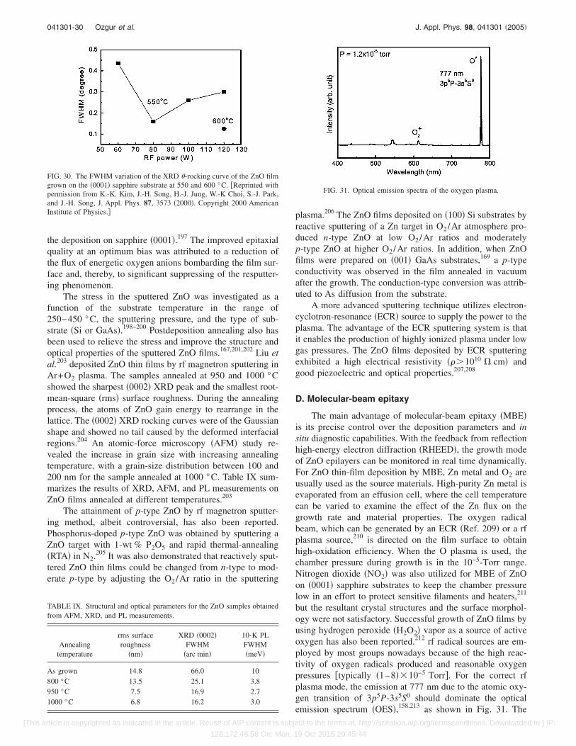
the deposition on sapphire �0001�.197 The improved epitaxialquality at an optimum bias was attributed to a reduction ofthe flux of energetic oxygen anions bombarding the film sur-face and, thereby, to significant suppressing of the resputter-ing phenomenon.
The stress in the sputtered ZnO was investigated as afunction of the substrate temperature in the range of250–450 °C, the sputtering pressure, and the type of sub-strate �Si or GaAs�.198–200 Postdeposition annealing also hasbeen used to relieve the stress and improve the structure andoptical properties of the sputtered ZnO films.167,201,202 Liu etal.203 deposited ZnO thin films by rf magnetron sputtering inAr+O2 plasma. The samples annealed at 950 and 1000 °Cshowed the sharpest �0002� XRD peak and the smallest root-mean-square �rms� surface roughness. During the annealingprocess, the atoms of ZnO gain energy to rearrange in thelattice. The �0002� XRD rocking curves were of the Gaussianshape and showed no tail caused by the deformed interfacialregions.204 An atomic-force microscopy �AFM� study re-vealed the increase in grain size with increasing annealingtemperature, with a grain-size distribution between 100 and200 nm for the sample annealed at 1000 °C. Table IX sum-marizes the results of XRD, AFM, and PL measurements onZnO films annealed at different temperatures.203
The attainment of p-type ZnO by rf magnetron sputter-ing method, albeit controversial, has also been reported.Phosphorus-doped p-type ZnO was obtained by sputtering aZnO target with 1-wt % P2O5 and rapid thermal-annealing�RTA� in N2.205 It was also demonstrated that reactively sput-tered ZnO thin films could be changed from n-type to mod-erate p-type by adjusting the O2/Ar ratio in the sputtering
plasma.206 The ZnO films deposited on �100� Si substrates byreactive sputtering of a Zn target in O2/Ar atmosphere pro-duced n-type ZnO at low O2/Ar ratios and moderatelyp-type ZnO at higher O2/Ar ratios. In addition, when ZnOfilms were prepared on �001� GaAs substrates,169 a p-typeconductivity was observed in the film annealed in vacuumafter the growth. The conduction-type conversion was attrib-uted to As diffusion from the substrate.
A more advanced sputtering technique utilizes electron-cyclotron-resonance �ECR� source to supply the power to theplasma. The advantage of the ECR sputtering system is thatit enables the production of highly ionized plasma under lowgas pressures. The ZnO films deposited by ECR sputteringexhibited a high electrical resistivity ���1010 � cm� andgood piezoelectric and optical properties.207,208
D. Molecular-beam epitaxy
The main advantage of molecular-beam epitaxy �MBE�is its precise control over the deposition parameters and insitu diagnostic capabilities. With the feedback from reflectionhigh-energy electron diffraction �RHEED�, the growth modeof ZnO epilayers can be monitored in real time dynamically.For ZnO thin-film deposition by MBE, Zn metal and O2 areusually used as the source materials. High-purity Zn metal isevaporated from an effusion cell, where the cell temperaturecan be varied to examine the effect of the Zn flux on thegrowth rate and material properties. The oxygen radicalbeam, which can be generated by an ECR �Ref. 209� or a rfplasma source,210 is directed on the film surface to obtainhigh-oxidation efficiency. When the O plasma is used, thechamber pressure during growth is in the 10−5-Torr range.Nitrogen dioxide �NO2� was also utilized for MBE of ZnOon �0001� sapphire substrates to keep the chamber pressurelow in an effort to protect sensitive filaments and heaters,211
but the resultant crystal structures and the surface morphol-ogy were not satisfactory. Successful growth of ZnO films byusing hydrogen peroxide �H2O2� vapor as a source of activeoxygen has also been reported.212 rf radical sources are em-ployed by most groups nowadays because of the high reac-tivity of oxygen radicals produced and reasonable oxygenpressures �typically �1–8��10−5 Torr�. For the correct rfplasma mode, the emission at 777 nm due to the atomic oxy-gen transition of 3p5P-3s5S0 should dominate the opticalemission spectrum �OES�,158,213 as shown in Fig. 31. The
FIG. 30. The FWHM variation of the XRD -rocking curve of the ZnO filmgrown on the �0001� sapphire substrate at 550 and 600 °C. �Reprinted withpermission from K.-K. Kim, J.-H. Song, H.-J. Jung, W.-K Choi, S.-J. Park,and J.-H. Song, J. Appl. Phys. 87, 3573 �2000�. Copyright 2000 AmericanInstitute of Physics.�
TABLE IX. Structural and optical parameters for the ZnO samples obtainedfrom AFM, XRD, and PL measurements.
Annealingtemperature
rms surfaceroughness
�nm�
XRD �0002�FWHM
�arc min�
10-K PLFWHM�meV�
As grown 14.8 66.0 10800 °C 13.5 25.1 3.8950 °C 7.5 16.9 2.71000 °C 6.8 16.2 3.0
FIG. 31. Optical emission spectra of the oxygen plasma.
041301-30 Ozgur et al. J. Appl. Phys. 98, 041301 �2005�
[This article is copyrighted as indicated in the article. Reuse of AIP content is subject to the terms at: http://scitation.aip.org/termsconditions. Downloaded to ] IP:
128.172.48.58 On: Mon, 19 Oct 2015 20:45:44

II/VI ratio can be tuned through the Zn cell temperature aswell as rf power and O2 flow rate of the plasma source. Forhigh-quality ZnO films, the reported growth temperature is inthe range of 350–650 °C with a growth rate of0.3–0.7 �m/h.157,158,214
In 1997 and 1998 Chen et al. reported ZnO epitaxialgrowth on �0001� sapphire substrates by using an oxygenmicrowave plasma source.158,180 The epitaxy process exhib-ited two-dimensional �2D� nucleation at the initial growthstage, which was followed by three-dimensional �3D� growthas indicated by RHEED. An in situ oxygen plasma preexpo-sure of the sapphire substrate was found to be critical for theinitial two-dimensional nucleation. The sapphire substrateswere exposed to the oxygen plasma for 30 min at 600 °Cbefore the growth. The preexposure produces an oxygen-terminated surface, which allows the first monolayer of ZnOto adjust itself to the oxygen sublattice of the Al2O3 substrateand thus to reduce the lattice mismatch. The XRD rockingcurve of ZnO showed a narrow �0002� peak �FWHM�0.005° � with a broad tail extending from the peak due tothe in-plane mosaicity. The PL spectra exhibited dominantbound-exciton emission with a FWHM of 3 meV at low tem-peratures and a free-exciton emission combined with a veryweak deep-level emission at RT.
The c plane of sapphire is composed of alternating layersof oxygen �sixfold symmetry� and Al atoms �threefold sym-metry�, while in the wurtzite structure of ZnO, both O andZn are sixfold symmetric about the ZnO c axis, as shown inFig. 28. For films grown on c-plane sapphire, the orientationrelationship along the direction normal to the surface is ZnO�0001� � sapphire �0001�, but two types of in-plane rotationaldomains are observed as a result of the following alignments:
ZnO �12̄10� � sapphire �11̄00� and ZnO �101̄0� � sapphire
�112̄0�.157,158 This corresponds to a 30° rotation between theZnO and sapphire a axes, presumably due to preferentialbonding of Zn atoms with sapphire O atoms. The presence ofthese domains leads to increased carrier scattering as exem-plified by the typical low mobilities of 10–40 cm2 V−1 s−1.
In order to eliminate the orientational domains often ob-
served in ZnO thin films grown on �0001� sapphire, �112̄0�sapphire substrates have been used for ZnO epitaxy. The lat-tice parameter a=0.3250 nm of ZnO and parameter c=1.299 nm of sapphire are related almost exactly by a factorof 4, with a mismatch less than 0.08% at room temperature.Based on this fact and coining the term “uniaxial lockedepitaxy,” Fons et al.210,215 conducted an investigation of ZnO
epitaxy growth on a-plane �112̄0� sapphire, including a de-tailed analysis of the initial stages of growth.216 The out-of-plane and in-plane orientational relationships are ZnO
�0001� � sapphire �112̄0� and ZnO �112̄0� � sapphire �0001�,respectively. The epitaxial relationship is shown in Fig. 32.As confirmed by the x-ray pole figure shown in Fig. 33, norotational domains or twins were present in the films. Theuse of a-plane sapphire substrates showed a significant im-provement compared to the c-plane sapphire substrates. Theresidual carrier concentration was decreased to 6�1016 cm−3 with electron mobility over 120 cm2 V−1 s−1.AFM revealed a rms roughness of less than 0.4 nm.
The effects of substrate offset angle on MBE growth ofZnO on c-plane sapphire were investigated by Sakurai et
al.217 Twin-crystal RHEED patterns from both �101̄0� and
�112̄0� planes and surface faceting observed withc-plane-oriented substrates were suppressed by enlarging theoffset angles from near 0° to 2.87°, tilted from c-plane to-ward the a-axis direction. As a result, improvement in crystalstructure and surface morphology was observed.
Different surface chemistries of sapphire substrates canlead to different growth modes. The surface chemistry of
�112̄0�-oriented sapphire was alternated from O rich to Alrich by changing the pregrowth treatment from oxygenplasma to atomic hydrogen.218 The two-dimensional growthwas more favorable and continued longer on a hydrogen-treated surface, although the initial two-dimensional growthwas eventually taken over by a three-dimensional growth forboth types of pretreatments. Figure 34 shows different ZnO
FIG. 32. Schematic diagram of the atom positions for basal ZnO grown ona-plane sapphire. The dots mark the O-atom positions and the dashed linesshow the sapphire a-plane unit cells. The open squares mark the Zn-atompositions and the solid lines show the ZnO basal-plane unit cell.
FIG. 33. Stereographic projections of the x-ray pole figure results for the
ZnO �101̄1� reflection for a ZnO film grown on �a� �inset� a c-plane sapphiresubstrate and �b� an a-plane sapphire substrate. The in-plane orientation of
sapphire is indicated by a sapphire �112̄6� measurement �filled circles�. �Re-printed with permission from P. Fons, K. Iwata, A. Yamada, K. Matsubara,S. Niki, K. Nakahara, T. Tanabe, and H. Takasu, Appl. Phys. Lett. 77, 1801�2000�. Copyright 2000 American Institute of Physics.�
041301-31 Ozgur et al. J. Appl. Phys. 98, 041301 �2005�
[This article is copyrighted as indicated in the article. Reuse of AIP content is subject to the terms at: http://scitation.aip.org/termsconditions. Downloaded to ] IP:
128.172.48.58 On: Mon, 19 Oct 2015 20:45:44
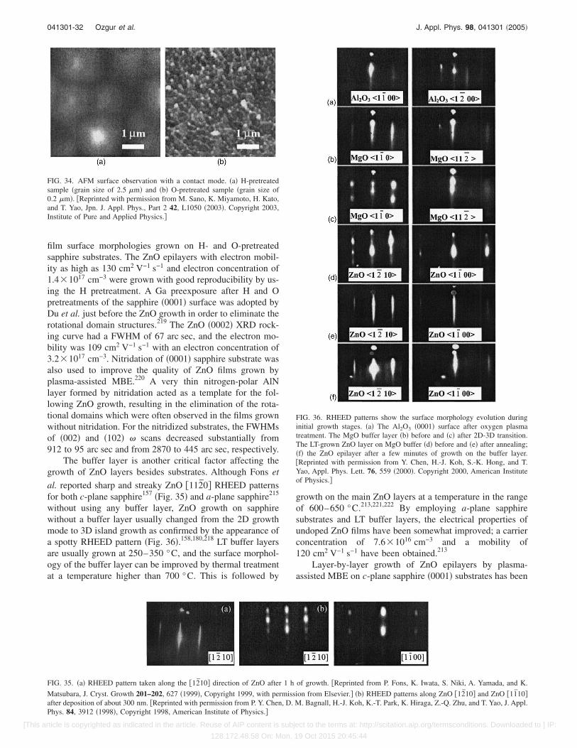
film surface morphologies grown on H- and O-pretreatedsapphire substrates. The ZnO epilayers with electron mobil-ity as high as 130 cm2 V−1 s−1 and electron concentration of1.4�1017 cm−3 were grown with good reproducibility by us-ing the H pretreatment. A Ga preexposure after H and Opretreatments of the sapphire �0001� surface was adopted byDu et al. just before the ZnO growth in order to eliminate therotational domain structures.219 The ZnO �0002� XRD rock-ing curve had a FWHM of 67 arc sec, and the electron mo-bility was 109 cm2 V−1 s−1 with an electron concentration of3.2�1017 cm−3. Nitridation of �0001� sapphire substrate wasalso used to improve the quality of ZnO films grown byplasma-assisted MBE.220 A very thin nitrogen-polar AlNlayer formed by nitridation acted as a template for the fol-lowing ZnO growth, resulting in the elimination of the rota-tional domains which were often observed in the films grownwithout nitridation. For the nitridized substrates, the FWHMsof �002� and �102� � scans decreased substantially from912 to 95 arc sec and from 2870 to 445 arc sec, respectively.
The buffer layer is another critical factor affecting thegrowth of ZnO layers besides substrates. Although Fons et
al. reported sharp and streaky ZnO �112̄0� RHEED patternsfor both c-plane sapphire157 �Fig. 35� and a-plane sapphire215
without using any buffer layer, ZnO growth on sapphirewithout a buffer layer usually changed from the 2D growthmode to 3D island growth as confirmed by the appearance ofa spotty RHEED pattern �Fig. 36�.158,180,218 LT buffer layersare usually grown at 250–350 °C, and the surface morphol-ogy of the buffer layer can be improved by thermal treatmentat a temperature higher than 700 °C. This is followed by
growth on the main ZnO layers at a temperature in the rangeof 600–650 °C.213,221,222 By employing a-plane sapphiresubstrates and LT buffer layers, the electrical properties ofundoped ZnO films have been somewhat improved; a carrierconcentration of 7.6�1016 cm−3 and a mobility of120 cm2 V−1 s−1 have been obtained.213
Layer-by-layer growth of ZnO epilayers by plasma-assisted MBE on c-plane sapphire �0001� substrates has been
FIG. 34. AFM surface observation with a contact mode. �a� H-pretreatedsample �grain size of 2.5 �m� and �b� O-pretreated sample �grain size of0.2 �m�. �Reprinted with permission from M. Sano, K. Miyamoto, H. Kato,and T. Yao, Jpn. J. Appl. Phys., Part 2 42, L1050 �2003�. Copyright 2003,Institute of Pure and Applied Physics.�
FIG. 35. �a� RHEED pattern taken along the �12̄10� direction of ZnO after 1 h of growth. �Reprinted from P. Fons, K. Iwata, S. Niki, A. Yamada, and K.
Matsubara, J. Cryst. Growth 201–202, 627 �1999�, Copyright 1999, with permission from Elsevier.� �b� RHEED patterns along ZnO �12̄10� and ZnO �11̄10�after deposition of about 300 nm. �Reprinted with permission from P. Y. Chen, D. M. Bagnall, H.-J. Koh, K.-T. Park, K. Hiraga, Z.-Q. Zhu, and T. Yao, J. Appl.Phys. 84, 3912 �1998�, Copyright 1998, American Institute of Physics.�
FIG. 36. RHEED patterns show the surface morphology evolution duringinitial growth stages. �a� The Al2O3 �0001� surface after oxygen plasmatreatment. The MgO buffer layer �b� before and �c� after 2D-3D transition.The LT-grown ZnO layer on MgO buffer �d� before and �e� after annealing;�f� the ZnO epilayer after a few minutes of growth on the buffer layer.�Reprinted with permission from Y. Chen, H.-J. Koh, S.-K. Hong, and T.Yao, Appl. Phys. Lett. 76, 559 �2000�. Copyright 2000, American Instituteof Physics.�
041301-32 Ozgur et al. J. Appl. Phys. 98, 041301 �2005�
[This article is copyrighted as indicated in the article. Reuse of AIP content is subject to the terms at: http://scitation.aip.org/termsconditions. Downloaded to ] IP:
128.172.48.58 On: Mon, 19 Oct 2015 20:45:44

achieved by introducing a thin MgO buffer.181,223,224 Theionic radius of Mg2+ is close to that of Zn2+,225 so the re-placement of Zn by Mg is not expected to induce a signifi-cant change for the lattice constants of MgZnO alloys. Theincorporation of MgO buffer is very effective in improvingthe surface morphology during the initial stages of growthand leads to an atomically flat surface. The 3�3 surfacereconstruction of ZnO was observed from RHEED �see Fig.36�. The twin defects with a 30° in-plane crystal-orientationmisalignment were completely eliminated and the total dis-location density was reduced as confirmed by small line-
widths of 13 and 84 arc sec observed for �0002� and �101̄5��-rocking curves, respectively.181 The �111�-oriented rock-salt MgO grows on sapphire �0001� with the following epi-
taxial relationship: MgO �11̄0� � sapphire �21̄1̄0� and
MgO �1̄1̄2� � sapphire �011̄0�.When the effects of the substrate orientation and buffer
layers are considered, homoepitaxy of ZnO seems to be themost efficient way to improve the overall properties.186 ZnOfilms have been grown on Zn-polar ZnO substrates, and two-dimensional growth with a smooth surface has been obtainedunder the O-rich flux condition. In addition to the improve-ment in the structural and optical properties, due to the re-duction in density of the edge-type threading dislocation, theresidual carrier concentration in the homoepitaxial ZnO filmswas as low as 2.2�1016 cm−3, and the electron mobility of158 cm2/V s was achieved.
The II/VI ratio has been studied for its effects on thesurface morphology and electrical properties. Figure 37shows the change of growth rate with Zn/O ratio.226 ZnOthin films with a MgO buffer layer were grown on c-planesapphire substrate. ZnO layers grown under stoichiometricand O-rich flux conditions show larger hexagonal islands of3000-nm diameter, whereas those grown under Zn-rich fluxconditions show smaller hexagonal islands of 200-nm diam-eter. The ZnO film was found to have O polarity. The ob-served surface morphology can be explained by the fact thatfor growth conducted on the O-polar surface, the surfacediffusion length of Zn adatoms was smaller under the Zn-rich condition than under the stoichiometric or O-rich condi-tion. ZnO layers grown under stoichiometric flux conditions
had high crystalline quality, the lowest dislocation density,and the highest electron mobility ��130 cm2 V−1 s−1� whencompared with ZnO films grown under nonstoichiometricflux conditions.
The control of the film polarity is an important issue inepitaxial growth of ZnO. When the film is grown in the�0001� direction, Zn polarity �+c� is obtained and the topsurface is Zn terminated. Likewise when the growth is in the
�0001̄� direction, O polarity �−c� is obtained and the topsurface is O terminated. Much effort has been expended todetermine the effects of polarity and to find a way of con-trolling the polarity during growth. The ZnO films grown byplasma-assisted MBE on as-polished �0001� sapphire sub-strates with or without a MgO buffer layer have Opolarity158,227,228 mainly due to the growth conditions. Thesapphire surface should be O terminated, since sapphire sub-strates are treated at elevated temperatures �600–700 °C� byO plasma prior to the growth. MgO buffer under the oxygenambient most likely has O-stabilized MgO surface. As dem-onstrated for atomically flat sapphire �0001� substrates, thepolarity of ZnO grown by laser MBE is closely correlatedwith the in-plane orientation of ZnO, i.e.,
ZnO �101̄0� �Al2O3 �112̄0� in the case of O polarity and
ZnO �112̄0� �Al2O3 �112̄0� in the case of Zn polarity.229 ZnOfilms with Zn polarity are preferentially obtained at lowgrowth temperature and high growth rate. The control overthe ZnO surface polarity has also been achieved on GaNsubstrates by plasma-assisted MBE.228,230 As confirmed bythe coaxial impact collision ion scattering spectroscopy�CAICISS� �see Fig. 38�, Zn- and O-polar ZnO films weresuccessfully grown with Zn- and O-plasma preexposures onGa-polar GaN templates prior to ZnO growth, respectively.
Although ZnO films grown on sapphire have shownpromising electrical and optical properties as discussedabove, the crystal quality still needs improvement, since highdensity of defects are present at the interface and throughoutthe films as a consequence of a large lattice mismatch �18%�between ZnO and sapphire. On the other hand, GaN is aclosely lattice-matched material to ZnO with a lattice mis-match of 1.8%. In this vein, Ko et al.231 studied the growthand characteristics of as-grown and annealed ZnO thin filmswith LT buffer layers on �0001� GaN templates grown byMOCVD on sapphire. The LT ZnO buffer layers were grownat 250–300 °C, and the surface was dramatically improvedby a thermal treatment above 600 °C.232 The growth tem-perature for the top ZnO layer was in the range from500 to 700 °C. A 3�3 RHEED pattern was observed duringcooling for the flat ZnO surface �see Fig. 39�.232
Ko et al.231 also studied the possibility of controlling theZnO/GaN interface by employing different surface-treatment procedures prior to ZnO growth.233 A treatment ofthe GaN surface by using Zn- or oxygen-plasma preexpo-sures affects the subsequent ZnO growth in different ways.The Zn pretreatment provides a well-ordered GaN surfacewithout any interface layer, while the oxygen-plasma pre-treatment results in the formation of a disordered surface dueto the formation of a Ga2O3 interface layer. Accordingly, thestructural and optical properties of Zn-exposed samples are
FIG. 37. Growth rate of ZnO layers against Zn beam flux. �Reprinted withpermission from H. Kato, M. Sano, K. Miyamoto, and T. Yao, Jpn. J. Appl.Phys., Part 1 42, 2241 �2003�. Copyright 2003, Institute of Pure and AppliedPhysics.�
041301-33 Ozgur et al. J. Appl. Phys. 98, 041301 �2005�
[This article is copyrighted as indicated in the article. Reuse of AIP content is subject to the terms at: http://scitation.aip.org/termsconditions. Downloaded to ] IP:
128.172.48.58 On: Mon, 19 Oct 2015 20:45:44
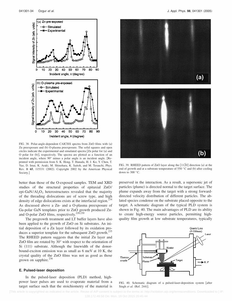
better than those of the O-exposed samples. TEM and XRDstudies of the structural properties of epitaxial ZnO/epi-GaN/Al2O3 heterostructures revealed that the majorityof the threading dislocations are of screw type, and highdensity of edge dislocations exists at the interfacial region.234
As discussed above a Zn- and a O-plasma preexposure ofGa-polar GaN templates prior to ZnO growth produced Zn-and O-polar ZnO films, respectively.228,230
The pregrowth treatment and LT buffer layers have alsobeen applied to the growth of ZnO on Si substrates. An ini-tial deposition of a Zn layer followed by its oxidation pro-duces a superior template for the subsequent ZnO growth.235
The RHEED pattern suggests that the initial Zn layer andZnO film are rotated by 30° with respect to the orientation ofSi �111� substrate. Although the linewidth of the donor-bound-exciton emission was as small as 6 meV at 10 K, thecrystal quality of the ZnO films was not as good as thosegrown on sapphire.236
E. Pulsed-laser deposition
In the pulsed-laser deposition �PLD� method, high-power laser pulses are used to evaporate material from atarget surface such that the stoichiometry of the material is
preserved in the interaction. As a result, a supersonic jet ofparticles �plume� is directed normal to the target surface. Theplume expands away from the target with a strong forward-directed velocity distribution of different particles. The ab-lated species condense on the substrate placed opposite to thetarget. A schematic diagram of the typical PLD system isshown in Fig. 40. The main advantages of PLD are its abilityto create high-energy source particles, permitting high-quality film growth at low substrate temperatures, typically
FIG. 38. Polar-angle-dependent CAICISS spectra from ZnO films with �a�Zn preexposure and �b� O-plasma preexposure. The solid squares and opencircles indicate the experimental and simulated spectra �Zn polar for �a� andO polar for �b��, respectively. The spectra are plotted as a function of anincident angle, where 90° minus a polar angle is an incident angle. �Re-printed with permission from S. K. Hong, T. Hanada, H. J. Ko, Y. Chen, T.Yao, D. Imai, K. Araki, M. Shinohara, K. Saitoh, and M. Terauchi, Phys.Rev. B 65, 115331 �2002�. Copyright 2002 by the American PhysicalSociety.�
FIG. 39. RHEED pattern of ZnO layer along the �112̄0� direction �a� at theend of growth and at a substrate temperature of 550 °C and �b� after coolingdown to 300 °C.
FIG. 40. Schematic diagram of a pulsed-laser-deposition system �afterSingh et al. �Ref. 244��.
041301-34 Ozgur et al. J. Appl. Phys. 98, 041301 �2005�
[This article is copyrighted as indicated in the article. Reuse of AIP content is subject to the terms at: http://scitation.aip.org/termsconditions. Downloaded to ] IP:
128.172.48.58 On: Mon, 19 Oct 2015 20:45:44

ranging from 200 to 800 °C, its simple experimental setup,and operation in high ambient gas pressures in the10−5–10−1-Torr range. For the growth of ZnO by PLD tech-nique, usually UV excimer lasers �KrF: =248 nm and ArF:=193 nm� and Nd: yttrium aluminum garnet �YAG� pulsedlasers �=355 nm� are used for ablation of the ZnO target inan oxygen environment. In some cases, Cu-vapor laser emit-ting at =510–578 nm �Ref. 237� was also used for thesame purpose. Cylindrical ZnO tablets made from pressedZnO powder are usually used as targets. Single-crystal ZnOhas been used to grow high-quality ZnO thin films veryrecently.238 A pure Zn metal is used only in rare cases.239,240
The properties of the grown ZnO films depend mainly on thesubstrate temperature, ambient oxygen pressure, and laserintensity. Sankur and Cheung241 and Nakayama242 have re-ported on high-quality ZnO growth by PLD. However, theinfluence of the growth conditions on the ZnO properties wasstudied much later.243–246
Tsukazaki et al.238 reported the high-quality ZnO thin-film deposition on close lattice-mismatched hexagonalScAlMgO4 substrates by laser MBE at high growth tempera-tures up to 1000 °C. The growth direction is identified as
�0001̄� direction �oxygen face�. The FWHM of �0002� XRDrocking curve is less than 18 arc sec for 1-�m-thick ZnOfilms. By using the high-quality undoped ZnO films, theseauthors also demonstrated ZnO p-i-n homojunctions forlight-emitting diode �LED� application. Nitrogen was used asthe p-type dopant by applying a “repeated temperaturemodulation epitaxy” method.
Choopun et al.243 studied the influence of oxygen pres-sure on surface morphology and optoelectronic properties ofZnO films grown on sapphire �0001� by PLD. The films weregrown at an optimized growth temperature of 750 °C. Thegrowth was carried out under various oxygen backgroundpressures ranging from 10−5 to 10−1 Torr. All the ZnO layersgrown were found to be c-axis oriented. The films grownunder lower oxygen pressure regimes �10−5–10−4 Torr� hada c-axis lattice parameter 0.25% larger than that of the bulkmaterial. This effect was attributed to both oxygen deficiencyand compressive strain induced by the sapphire substrate.However, for the films deposited under higher oxygen pres-sures �10−2–10−1 Torr�, the c lattice constant was found toapproach the bulk value. The FWHM of XRD �-rockingcurve was 0.069° for the film grown at an O2 pressure of10−4 Torr. The in-plane ordering, as determined from XRD
� scans of the ZnO �101̄1� planes, however, was strongly
influenced by the oxygen pressure. The FWHMs of �101̄1�peaks were 0.43° and 0.78° for the ZnO films grown at 10−4
and 10−1 Torr, respectively.Figure 41 shows the surface morphology of the ZnO
films grown at various O2 pressures.243 The morphology ofthe films grown at 10−5–10−4 Torr was dominated by a typi-cal “honeycomblike” structure with 3D growth features asevidenced by the well-faceted hexagons �Fig. 41�a��. Thetransition towards the growth of a smooth film was found atan O2 pressure of 10−2 Torr. This change in the growth moderesulted in a substantial reduction of rms roughness to10–20 Å for a flat surface. A further increase of the O2 pres-
sure to 10−1 Torr showed an adverse effect on the surfacemorphology �Fig. 41�c�� typically featured by high nucle-ation densities, irregular grains with different sizes, and theincrease in surface roughness to about 400 Å.
The effect of oxygen pressure on the electrical properties�Hall mobility � and carrier concentration n� of the ZnOfilms is shown in Fig. 42.243 The highest electron mobility�72 cm2/V s� was obtained for the film grown at10−4–10−3 Torr, but this film also showed the highest carrierconcentration �7�1017 cm−3�. Further increase in O2 pres-sure reduced the Hall mobility, possibly as a result of elec-tron scattering by defects/ionized impurities. The opticalquality of the ZnO epilayer grown at 10−4 Torr was muchhigher than those grown at 10−1 Torr, as evidenced by amuch higher excitonic luminescence intensity �by two ordersof magnitude�. This indicates that a high concentration ofdefects in ZnO film affects the radiative processes.
As seen from the above results, the PLD growth of high-quality epitaxial ZnO films with smooth surfaces and desir-able electrical and optical properties has different optimumoxygen pressure regimes. To overcome this problem, a two-step growth procedure has been developed.243 In this process,the nucleation layer is grown at low oxygen pressure�10−4 Torr�, which produces a high-quality template for thesubsequent growth of ZnO at a high oxygen pressure�10−1 Torr�.
The preparation of highly conducting and transparentaluminum-doped zinc oxide films was reported by Singh etal.244 The films were deposited on quartz and Corning 7059glass by focusing a XeCl �=308 nm and 20-ns pulse width�excimer laser onto a target rotating at 15 rpm. The ZnO tar-get was 2 in. in diameter and doped with 2-wt % Al2O3. Forall the experiments, a repetition rate of 5 Hz and an energy
FIG. 41. AFM images of the ZnO films grown at various oxygen pressures:�a� 10−4 Torr, �b� 10−2 Torr, �c� 10−1 Torr, and �d� 10−1 Torr, with a nucle-ation layer of 100 Å grown at 10−4 Torr. �Reprinted with permission from S.Choopun, R. D. Vispute, W. Noch, A. Balsamo, R. P. Sharma, T. Venkatesan,A. Iliadis, and D. C. Look, Appl. Phys. lett. 75, 3947 �1999�. Copyright1999, American Institute of Physics.�
041301-35 Ozgur et al. J. Appl. Phys. 98, 041301 �2005�
[This article is copyrighted as indicated in the article. Reuse of AIP content is subject to the terms at: http://scitation.aip.org/termsconditions. Downloaded to ] IP:
128.172.48.58 On: Mon, 19 Oct 2015 20:45:44

density of 1.5 J /cm2 were used. The distance between thetarget and the substrate was 30 mm, and the deposition timewas kept at 30 min. The effects of substrate temperature�from room temperature to 400 °C� and oxygen pressure�from 0.1 to 5 mTorr� were investigated by analyzing theoptical and electrical properties of the films. The averagetransmittance was found to be in the range of 86%–92%, andresistivity varied from 3.56�10−3 to 7.0�10−3 � cm. Thelowest resistivity measured was 1.4�10−4 � cm for thefilms grown at 300 °C and 1 mTorr oxygen pressure.
Matsubara et al.245 used oxygen radical-assisted PLD togrow highly transparent and low-resistivity Al-doped ZnOfilms at room temperature. A KrF excimer laser �=248 nm, 30-ns pulse width, and 10-Hz repetition rate� wasused for ablation. The oxygen partial pressure during depo-sition was �0.7–1.4��10−5 Torr, and the applied rf powerwas 150 W. The distance between the target and the sub-strate was approximately 6 cm. The minimum resistivity ofthe obtained transparent films was 5�10−4 � cm. The aver-age transmittance in the visible wavelength region was over86% for �0.7-�m-thick films. The films grown in a low-pressure molecular-oxygen atmosphere �1.4�10−5 Torr�were slightly black and had low transmittance in the visibleand near infrared regions of the optical spectrum, and hadrelatively lower resistivity. The radical source assisted theincorporation of oxygen into the films and made the filmstransparent.
Craciun et al.246 deposited high-quality ZnO films onglass and silicon substrates by the PLD technique employinga KrF laser �=248 nm�, and studied the influence of the
deposition parameters, such as substrate temperature, oxygenpressure, and laser fluence, on the properties of the grownfilms. All the films grown over a rather wide range of depo-sition conditions were found to be optically transparent, elec-trically conductive, and c-axis oriented, with the FWHM ofthe �002� XRD line being very often less than 0.25°. Inves-tigations of the effect of different oxygen partial pressuresshowed that the best-quality films could be obtained in thehigher pressure range, i.e., between 1�10−3 and4�10−3 Torr. This result is quite different from that ob-tained previously, and has been accounted for by the differ-ences in the substrate-to-target distances employed. The elec-trical resistivity of the films was strongly affected by theoxygen pressure, increasing from �7–9��10−3 � cm for thefilms deposited at 2�10−5 Torr to �5–8��10−2 � cm forthose deposited at 2�10−3 Torr. This behavior can be easilyunderstood by taking into account that the electrical conduc-tivity of ZnO is controlled by Zn interstitials or O vacancies.From these studies it was concluded that the best conditionsfor PLD of ZnO films center around substrate temperaturesbetween 300 and 350 °C, oxygen partial pressures from1�10−3 to 2�10−3 Torr, and a laser fluence of around2 J /cm2. Within this range, the FWHM of the �002� XRDline is always below 0.18° and the transparency is above85% in the visible region of the spectrum. Figure 43 showsthe XRD pattern recorded for a ZnO film grown with a flu-ence of 2.1 J /cm2, substrate temperature of 350 °C, andoxygen pressure of 2�10−3 Torr.246 Only the �002� and�004� XRD lines are present along with the Si �100� peak ofthe substrate. The FWHM of the �002� reflection was 0.13°,one of the lowest values yet reported in the literature forPLD-grown ZnO. The small peak at around 10° was attrib-uted to the presence of a very thin amorphous transitionallayer between the Si substrate and the grown ZnO film. Therocking curve measured for the �002� diffraction, as shown inthe inset of Fig. 43, is at 16.99° with a FWHM of 2.07°.
F. Chemical-vapor deposition
Among other growth methods, chemical-vapor deposi-tion �CVD� technology is particularly interesting not only
FIG. 42. Hall mobility and carrier concentration vs oxygen pressure for ZnOgrowth. For comparison, the data for the ZnO film grown at 10−1 Torr withthe nucleation layer grown at 10−4 Torr are also shown. �Reprinted withpermission from S. Choopun, R. D. Vispute, W. Noch, A. Balsamo, R. P.Sharma, T. Venkatesan, A. Iliadis, and D. C. Look, Appl. Phys. Lett. 75,3947 �1999�. Copyright 1999, American Institute of Physics.�
FIG. 43. XRD pattern of a ZnO thin film deposited under optimized condi-tions. The rocking curve recorded for the �002� line is shown in the inset.�Reprinted with permission from V. Craciun, J. G. E. Gardeniers, and I. W.Boyd, Appl. Phys. Lett. 65, 2963 �1994�. Copyright 1994, American Insti-tute of Physics.�
041301-36 Ozgur et al. J. Appl. Phys. 98, 041301 �2005�
[This article is copyrighted as indicated in the article. Reuse of AIP content is subject to the terms at: http://scitation.aip.org/termsconditions. Downloaded to ] IP:
128.172.48.58 On: Mon, 19 Oct 2015 20:45:44

because it gives rise to high-quality films but also because itis applicable to large-scale production. This technique iswidely used in the fabrication of epitaxial films toward vari-ous GaN-based optoelectronic devices, and similar trendmight be expected for future applications of ZnO. There areseveral modifications of this method depending on precur-sors used. When metal-organic precursors are used, the tech-nique is called MOCVD,160 metal-organic vapor-phase epi-taxy �MOVPE�, or organometallic vapor-phase epitaxy�OMVPE�. In the case of hydride or halide precursors, thetechnique is named hydride or halide CVD or VPE.161,162
In the CVD method, ZnO deposition occurs as a result ofchemical reactions of vapor-phase precursors on the sub-strate, which are delivered into the growth zone by the car-rier gas. The reactions take place in a reactor where a neces-sary temperature profile is created in the gas flow direction.
For hydride VPE growth of ZnO, hydrogen �H2� wasemployed as a carrier gas.247–249 In these particular cases, thetypical pressure was �133 Pa and the flow rate was about40 ml/min. Targets made from ZnO powder were placed inthe evaporation zone in which the temperature was around770 °C. The following chemical reaction between the ZnOtarget and H2 carrier gas takes place in the evaporation zone:
ZnO + H2 → Zn + H2O.
On the substrate �the deposition zone�, where the tempera-ture was kept in the range of 590–610 °C, the reverse reac-tion occurs:
Zn + H2O → ZnO + H2.
The ZnO films grown by this method show quite high crys-tal, electrical, and luminescence properties.250,251
ZnO films were also grown by halide VPE employingoxygen gas and Zn chloride �ZnCl2� �Ref. 162� or Zn iodide�ZnI2� �Ref. 252� as sources of Zn and O, respectively. It wasdemonstrated that the iodide system allows growing ZnOlayers of higher optical and structural properties. The mainadvantage of this technique is its very high growth rate. Thepreparation of 100-�m ZnO films showing room-temperature ultraviolet emission with a PL FWHM as narrowas 10 meV was reported by Takashi et al.253
For ZnO growth, MOCVD/MOVPE technique typicallyinvolves the use of metal alkyls, usually dimethyl zinc��CH3�2Zn� �DMZn� or diethyl zinc ��C2H5�2Zn� �DEZn� incombination with a separate source of oxygen and argon ornitrogen as a carrier gas. In earlier investigations, O2 or H2Owere used as oxygen precursors.37,254,255 However, DEZnand DMZn are highly reactive with oxygen and water vaporso that severe premature reaction in the gas phase occurs inthe cold zone of the reactor, resulting in the formation ofwhite powder, that degrades the film quality. Nevertheless,great progress has been made in ZnO growth by MOCVDrecently. The improvement of the material quality is relatedto improved reactor design256 and/or the use of less-reactiveprecursors, allowing one to minimize parasitic prereactionsin the gas phase. Stable metal-organic source of zinc acety-lacetonate in combination with oxygen was successfully usedfor the growth of high-quality ZnO films on r-plane257 aswell as on c- and a-plane258 sapphire substrates by atmo-
spheric pressure MOCVD. For the group-VI precursor, a va-riety of oxygen compounds were employed: isopropanol�i-PrOH�,259–262 tertiary-butanol �t-BuOH�,263–266 acetone,37
N2O,37,267–270 and NO2.258
High-quality ZnO layers have been prepared onGaN/sapphire259,261 and c-plane sapphire252,260 substrates byusing DEZn and i-PrOH. FWHMs of the �-2 scans were100 and 270 arc sec depending on the substrate, and the5-K PL spectra showed strong near-band-edge emission withline widths of 5–12 meV with phonon replicas.251,259 For thefilms grown on c-plane sapphire under optimized conditions,PL was dominated by strong near-band-edge lines withFWHM below 4 meV, and the excitonic signals were clearlyvisible in reflectivity measurements.260 Hall-effect measure-ments indicated an n-type background doping in the1017-cm−3 range with carrier mobilities of more than100 cm2/V s.
Kirchner et al.266 have reported direct comparison ofMOVPE growth of ZnO layers on c-plane sapphire usingi-PrOH and t-BuOH as oxygen precursors and DEZn as azinc source. It has been demonstrated that the two oxygenprecursors show similar pressure dependence of the ZnOgrowth rate but large differences in temperature-dependentgrowth rate �see Fig. 44�. The growth rate was found to bealmost constant over a wide temperature range from380 to 510 °C in the case of t-BuOH, whereas for i-PrOHthe maximum growth rate was achieved at 380 °C. The op-tical quality of the ZnO layers grown with t-BuOH weresuperior to those grown with i-PrOH. For ZnO grown underoptimized conditions using t-BuOH, strong near-band-edgeemission lines with half-widths of 1.1 meV dominated thePL spectra.
Great potential of nitrous oxide for MOVPE of ZnO wasdemonstrated by Ogata et al.267 Low reactivity allows one togrow ZnO films at a high substrate temperature that results inhigh crystal perfection and good optical quality of the mate-rial. Oleynik et al.262 reported superior characteristics of ZnOlayers grown on GaN/Si substrates with the use of N2Ocompared to those prepared with i-PrOH and acetone. The
FIG. 44. Temperature dependence of the ZnO growth rate using isopropanol�black rectangles� or tertiary butanol �black circles� as the oxygen precursor.The DEZn flow rate is 100 �mol/min. The reactor pressure for both sets ofsamples is 400 mbars. �Reprinted from C. Kirchner, T. Gruber, F. Reuss, K.Thonke, A. Waag, C. Giessen, and M. Heuken, J. Cryst. Growth 248, 20�2003�, Copyright 2003, with permission from Elsevier.�
041301-37 Ozgur et al. J. Appl. Phys. 98, 041301 �2005�
[This article is copyrighted as indicated in the article. Reuse of AIP content is subject to the terms at: http://scitation.aip.org/termsconditions. Downloaded to ] IP:
128.172.48.58 On: Mon, 19 Oct 2015 20:45:44

growth of a LT- �500 °C� buffer layer of ZnO was demon-strated to be essential to enhance the initial nucleation pro-cess and to achieve high-quality ZnO overgrown layers athigher growth temperatures �600–700 °C�.267 Dadgar etal.270 used t-BuOH and DEZn as precursors for the growthof LT �450 °C� ZnO buffers on GaN/sapphire substrates. Atthe second stage, ZnO layers were grown at a high tempera-ture �900–950 °C� using N2O. The layers showed smoothsurface morphology and high crystalline quality as demon-strated by XRD �FWHM of �0002� � scans for a2.28-�m-thick layer was 160 arc sec�. The bright lumines-cence was dominated by narrow excitonic �FWHM�1.3 meV� emission lines. The effects of LT-buffer thick-ness as well as substrate temperature on the optical quality ofZnO layers were studied systematically �see Fig. 45�.
High-quality homoepitaxial ZnO layers were grown onbulk ZnO substrates by using N2O and DEZn.271 Two con-ditions, proper thermal treatment of substrate prior to thegrowth to obtain a flat surface and high flow-rate ratios ofsource materials, were found to be important to obtain high-quality layers. Surface roughness below 1 nm as well asstrong free-exciton emission at 15 K was reported for thefilms grown under optimal conditions.
The improvement of MOCVD technology also gave riseto great progress in the quality of ZnO layers grown with theuse of DEZn and O2. The pressure used for the growth wasin the range of 5–250 Torr.272,273 Lower-pressure effect wasinvestigated and the results showed that the crystal qualitywas better for films grown at 6 Torr than those grown at0.05 Torr.274 R-plane sapphire substrate has been used inMOCVD growth of ZnO.272 The epitaxial relationship be-tween ZnO and R-plane sapphire was found to be
�112̄0�ZnO � �011̄2� sapphire and �0001�ZnO � �01̄11� sap-phire. Figure 46 shows the epitaxial relationship. High-crystallinity ZnO epilayers were grown on sapphire �0001�substrates with LT ZnO buffer layer.273 The XRD rockingcurve data of as-grown films exhibited FWHM values in therange of 0.04°–0.05°.
The in-plane orientation of ZnO epitaxial films grownon as-polished �0001� sapphire substrates by MOCVD hasbeen reported to depend on the initial conditions whenstarting the flow of DEZn over the substrate.275 The epi-taxial orientation can easily be controlled to be either
ZnO �112̄0� � sapphire�112̄0� �no in-plane rotation� or ZnO
�101̄0� � sapphire�112̄0� �30° in-plane rotation�, but all thefilms had Zn polarity regardless of the in-plane orientation,in contrast to the result obtained by MBE.229
The effect of oxygen partial pressure on the structuralperfection as well as optical and electrical properties of ZnOfilms grown at 600 °C on Al2O3 �0001� was studied by Maet al.276 It was found that the conduction type in undopedZnO layers could be controlled by adjusting the oxygen par-tial pressure during growth. The films grown under an oxy-gen partial pressure lower than 45 Pa showed n-type conduc-tivity. With increasing oxygen pressure, the crystallinity ofthe ZnO layers degraded to polycrystalline with additional
�101̄2� orientation, and intrinsic p-type ZnO �which shouldbe treated with some caution� was produced as the oxygenpartial pressure became higher than 55 Pa. The hole concen-tration and mobility reached 1.59�1016 cm−3 and9.23 cm2/V s, and the resistivity was 42.7 � cm. The near-band-edge and deep-level emissions in RT PL spectra wereinfluenced strongly by the oxygen partial pressure.Temperature-dependent PL spectra in n-type ZnO filmsshowed a dominant neutral-donor-bound-exciton emission,while the p-ZnO was dominated by the neutral-acceptor-bound-exciton line. With decreasing temperature, both peaksincreased in intensity and blueshifted. The band that origi-nated from zinc vacancies emerged for temperatures below155 K only in the p-type films. The origin of intrinsic p-typeconductivity in ZnO thin films was attributed to zinc vacan-cies, the premise of which should be treated with a great dealof caution.
Evolution and growth of ZnO films grown onGaN/AlN/SiC �0001� �Refs. 277 and 278� and ZnO �Ref.279� from DEZn and O2 have been reported by Smith et al.From a microscopic study of initial growth stages it wasconcluded that ZnO on GaN templates nucleated and grewvia the Stranski-Krastanov mode.277 At 500 °C, dense ZnO
FIG. 45. CL linewidth of the ZnO near band-edge emission as a function ofLT buffer layer thickness and growth temperature. The linewidth decreaseswith increasing growth temperature and with increasing layer thickness ofthe LT ZnO buffer. �Reprinted from A. Dadgar, N. Oleynik, D. Forster, S.Deiter, H. Witek, J. Blasing, F. Bertramm, A. Krtschil, A. Diez, J. Christen,and A. Frost, J. Cryst. Growth 267, 140 �2004�, Copyright 2004, with per-mission from Elsevier.�
FIG. 46. Epitaxial relationships of a-plane ZnO grown on R-plane Al2O3.
041301-38 Ozgur et al. J. Appl. Phys. 98, 041301 �2005�
[This article is copyrighted as indicated in the article. Reuse of AIP content is subject to the terms at: http://scitation.aip.org/termsconditions. Downloaded to ] IP:
128.172.48.58 On: Mon, 19 Oct 2015 20:45:44
�0001� films formed via coalescence of islands either onGaN/AlN/SiC �0001� substrates or on initial, coherent ZnOlayers.278 To check the possible effect of interface oxide layeron the growth mode and film morphology, the GaN surfacewas preexposed to the reagents in different ways at the ini-tiation of growth. Interfaces between ZnO and GaN exposedeither simultaneously to diethylzinc and oxygen or only todiethylzinc were sharp and epitaxial. Interfaces formed afterthe exposure of the GaN to O2 were less coherent, though aninterfacial oxide was not observed by cross-sectionalTEM.278 A strong effect of the surface polarity was revealedfor homoepitaxial growth of ZnO films on O- and Zn-terminated ZnO �0001� substrates.279 The films, grown onO-terminated ZnO surfaces were initially dense. However,they changed to a textured polycrystalline microstructure af-ter approximately 100 nm and exhibited a surface roughnessof 7.3 nm. By contrast, the films grown on the Zn-terminatedsurface under the same conditions were fully dense, withouttexture, and appeared to be monocrystalline with a signifi-cantly improved surface roughness of 3.4 nm.
An important advantage of the MOCVD/MOVPE tech-nique is the feasibility of catalyst-free growth of ZnO nano-wires �nanorods�. For DEZn and N2O source materials,Ogata et al.280 demonstrated a possibility to control thegrowth mode by tuning the growth parameters. At lowertemperatures and/or lower VI/ II ratio, the growth tended tobe three-dimensional and nanorod structure could be grownon sapphire substrates. At higher temperatures two-dimensional growth was performed, and the flat and uniformepilayers could be formed both on sapphire and bulk ZnOsubstrates. The homoepitaxial ZnO layers exhibited a rmsvalue of 3 nm and a FWHM of 0.5 meV in low-temperature�9 K� PL emission. With the use of different precursor sys-tems, the MOCVD/MOVPE method was successfully ap-plied to the catalyst-free growth of ZnO nanowires on vari-ous substrates, such as Si,281,282 GaN/sapphire,281 c-planesapphire,281,283,284 and GaAs �001�.285 In the case of GaAssubstrate it was reported that, postgrowth heat treatment re-sulted in p-type doping of nanowires owing to As diffusionfrom GaAs substrate.285 Yang and Zhang 286 used MOCVDto grow ZnO single-crystal whiskers on glass substrates. Inorder to investigate the possibility of a combination of band-gap engineering and nanopillar growth, Kling et al.287 grewZnMgO nanorods. The Mg incorporation was confirmed byPL measurements and a blueshift of the band gap of up to170 meV could be achieved for the nanopillars with thehighest Mg concentration. Park et al.288 also demonstratedthe growth of ZnO/Zn0.8Mg0.2O nanorod single-quantum-well structures. Moreover, a fabrication of high-mobilityfield-effect transistors �FETs� using ZnO nanorods grown byMOVPE has been reported very recently.289 A high transcon-ductance of 1.9 �S and high electron mobility above1000 cm2/V s were achieved.
IV. OPTICAL PROPERTIES OF ZnO
A. Prelude
The optical properties of a semiconductor are connectedwith both intrinsic and extrinsic effects. Intrinsic optical tran-
sitions take place between the electrons in the conductionband and holes in the valence band, including excitonic ef-fects due to the Coulomb interaction. Excitons are classifiedinto free and bound excitons. In high-quality samples withlow impurity concentrations, the free exciton can also exhibitexcited states, in addition to their ground-state transitions.Extrinsic properties are related to dopants or defects, whichusually create discrete electronic states in the band gap, andtherefore influence both optical-absorption and emission pro-cesses. The electronic states of the bound excitons �BEs�depend strongly on the semiconductor material, in particular,the band structure. In theory, excitons could be bound toneutral or charged donors and acceptors. A basic assumptionin the description of the principal bound-exciton states forneutral donors and acceptors is a dominant coupling of thelike particles in the BE states. For a shallow neutral-donor-bound exciton �DBE�, for example, the two electrons in theBE state are assumed to pair off into a two-electron statewith zero spin. The additional hole is then weakly bound inthe net hole-attractive Coulomb potential set up by thisbound two-electron aggregate. Similarly, shallow-neutralacceptor-bound excitons �ABEs� are expected to have a two-hole state derived from the topmost valence band and oneelectron interaction. These two classes of bound excitons areby far the most important cases. Other defect-related transi-tions could be seen in optical spectra such as free to bound�electron-acceptor�, bound to bound �donor-acceptor�, andthe so-called yellow/green luminescence.
B. Optical transitions in ZnO
Optical transitions in ZnO have been studied by a varietyof experimental techniques such as optical absorption, trans-mission, reflection, photoreflection, spectroscopic ellipsom-etry, photoluminescence, cathodoluminescence, calorimetricspectroscopy, etc. In this section, a review on the intrinsicexcitonic properties is given first. The donor- and acceptor-bound excitons are discussed next. This is followed by adiscussion of two-electron satellites related to the donor-bound excitons. Finally, LO-phonon replicas of the main ex-citonic emissions and the donor-acceptor-pair �DAP� transi-tion are reviewed. The temperature dependence of the full PLspectrum is also explored and necessary arguments are madeto support the assignments for specific transitions. Thedefect-related transitions are discussed in detail in Sec. V.
1. Free excitons and polaritons
The wurtzite ZnO conduction band is mainly constructedfrom the s-like state having �7
c symmetry, whereas the va-lence band is a p-like state, which is split into three bandsdue to the influence of crystal-field and spin-orbitinteractions.290 The near-band-gap intrinsic absorption andemission spectrum is therefore dominated by transition fromthese three valence bands. The related free-exciton transi-tions from the conduction band to these three valence bandsor vice versa are usually denoted by A �also referred to as theheavy hole�, B �also referred to as the light hole�, and C �alsoreferred to as crystal-field split band�. However, the orderingof the crystal-field and spin-orbit coupling split states of the
041301-39 Ozgur et al. J. Appl. Phys. 98, 041301 �2005�
[This article is copyrighted as indicated in the article. Reuse of AIP content is subject to the terms at: http://scitation.aip.org/termsconditions. Downloaded to ] IP:
128.172.48.58 On: Mon, 19 Oct 2015 20:45:44

valence-band maximum in wurtzite ZnO has been a subjectof controversy.11,12,290–292 The essential difference has itsgenesis in the interpretation of the spectral line, which wasinitially assigned to the intrinsic ground-state A-exciton tran-sition by Thomas,11 and in contrast to extrinsic, ionizeddonor-bound-exciton complex transition, by Park et al.12 Re-cent availability of high-quality ZnO single crystals haspaved the way to observe intrinsic exciton transitions in low-temperature photoluminescence, magnetoluminescence, andreflectance measurements.291,293,294 Reynolds et al.291 ad-dressed this issue using second-order photoluminescencespectra, which helped resolve the additional fine structure ofthe excitons. They concluded that the valence-band symme-try ordering �A-�9, B-�7, and C-�7� in ZnO is not reversedbut the same as that observed in most other wurtzitic II-VIstructures and GaN. However, Lambrecht et al.295 arguedthat the analysis of Reynolds et al. was incorrect due to theirassumptions about the sign of the Lande g factor for holesand that the valence-band ordering is in fact A-�7, B-�9, andC-�7. Figure 47 shows the band diagram for the zinc-blendeand the wurtzite ZnO structures. �After Birman296 forvalence-band ordering A-�9, B-�7, and C-�7.�
Group-theory arguments and the direct product of thegroup representations of the band symmetries ��7 for theconduction band, �9 for the A valence band, upper �7 for Bvalence band, and lower �7 for C valence band� will result inthe following intrinsic exciton ground-state symmetries:
�7 � �9 → �5 + �6,
�7 � �7 → �5 + �1 + �2.
The �5 and �6 exciton ground states are both doubly degen-erate, whereas �1 and �2 are both singly degenerate. In ideal,i.e., strain-free, wurtzite crystals free excitons should obeythe selection rules in optical one-photon processes; �5 and �1
are allowed transitions with E�c and E �c polarizations, re-spectively, but the �6 and �2 are not allowed. Therefore, allthree excitons are allowed in the � polarization�E�c and k�c�, but the C exciton is quite weak. The Cexciton is strongly allowed in the � polarization �E �c andk�c�. However, the A exciton is forbidden and the B excitonis only weakly observable in this geometry. In the � polar-ization �E�c and k �c� all three transitions are clearly ob-servable. Each of these fundamental excitonic states are ex-pected to have a fine structure due both to exciton-polaritonlongitudinal-transverse splitting and the splitting caused byelectron-hole exchange interaction, which are on the order ofa few meV.22,297
The transition energies of the intrinsic excitons weremeasured by employing the low-temperature absorption,18,298
reflection,12,291,299 photoreflectance �PR�,300,301 and PL �Refs.299, 291, 293, and 294� spectroscopy techniques. Thesemeasurements pave the way for the determination of excitonbinding energies, exciton Bohr radii, the dielectric constant,and with the aid of the quasicubic model, spin-orbit andcrystal-field parameters. In this section, these optical proper-ties of the ZnO excitonic transitions will be discussed indetail.
In 1960, Thomas11 studied the fundamental absorptionedge and the exciton structure of ZnO. He measured thelow-temperature absorption and reflectance spectra of pol-ished and etched thin crystals grown from the vapor phase.Thomas analyzed the reflectance data by means of theKramers-Kronig relation and three peaks arising from n=1exciton transitions involving holes from each one of the threevalence bands. At 4.2 K the n=2 exciton states were appar-ent in reflection, allowing estimates to be made of the exci-ton binding energy and reduced mass. An example of a re-flectance spectra obtained in the � and � polarizations aregiven in Fig. 48 for a single-crystal ZnO sample.
Park et al.12 reported the fundamental spectra of ZnOand successfully explained the exciton spectrum on the basisof Birman’s model296 of the wurtzite structure analyzing theenergy and polarization of the fine structure around the fun-damental absorption region. Stimulated by these results,Hopfield and Thomas22 studied the polariton absorption linesin ZnO using a magnetic field in appropriate geometry to
FIG. 47. Band structure and selection rules for the ZB and W structures. Thecrystal field and spin-orbit splittings are indicated schematically. The tran-sitions which are allowed for various polarizations of photon electric-fieldvector with respect to the c axis are indicated �after Birman �Ref. 296��.
FIG. 48. Reflection from ZnO at 4.2 K for �a� E�c and�b� E �c. Notice the PL lines for the E�c data. �Re-printed from D. G. Thomas, J. Phys. Chem. Solids�15,86 �1960�, Copyright 1960, with permission fromElsevier.�
041301-40 Ozgur et al. J. Appl. Phys. 98, 041301 �2005�
[This article is copyrighted as indicated in the article. Reuse of AIP content is subject to the terms at: http://scitation.aip.org/termsconditions. Downloaded to ] IP:
128.172.48.58 On: Mon, 19 Oct 2015 20:45:44

allow couplings at polariton crossings. A satisfactory agree-ment was attained when the crossing frequencies of the po-lariton dispersion and light with E �c and E�c polarizationswere compared with the measured absorption line energies.Depending on their results Hopfield and Thomas also arguedthat the B exciton in fact belongs to the �9 symmetry group.
Among these publications, there exists a discrepancy inthe quoted values for the spin-orbit interaction energy andthe exciton binding energies, which most likely may have itsgenesis in the difficulty of interpreting the complex spectranear the band edge. The features associated with A-, B-, andC-exciton transitions, their excited states, and exciton-polariton and exciton-LO-phonon complexes are sometimesmisinterpreted, resulting in reports of different energy values.To shed additional light, Liang and Yoffe18 performedpolarization-dependent transmission measurements onsingle-crystal ZnO thin platelets grown by the vapor trans-port method. In addition to the transitions associated with theground, the first, and the second excited states of intrinsicexcitons, the exciton-phonon complexes were also observedin the transmission spectrum. In the same vein but later on,Reynolds et al.302 reported the shift in intrinsic exciton tran-sitions analyzing the reflection data from strained ZnO singlecrystals grown by the vapor transport method. Duringgrowth, defect complexes �probably pairs� are preferentiallyincorporated in certain crystallographic orientations, produc-ing compressive strain in the vicinity of the defect pairs withthe strain being oriented in the direction of the pair. By ob-serving the changes in emission from the defect pairs as theannealing temperature is increased, Reynolds et al.302 inves-tigated the relaxation of strain following an increase in thenumber of nearer pairs. Intrinsic energy bands were observedto adjust to these changes by moving to lower energies. Foran annealing temperature of 800 °C, shifts as much as0.4 meV for the A-exciton transition and 3 meV for theB-exciton transition were quoted for � polarization at 2 K.
Chichibu et al.301 studied the photoreflectance spectra ofhigh-quality ZnO epitaxial layers grown on ScAlMgO4 sub-strates by laser MBE and observed clear excitonic reso-nances due to the three excitons. A larger broadening wasobserved for the B and C excitons compared to the A exci-ton, which was interpreted to be due to a contribution by theexciton polaritons in terms of large longitudinal-transversesplitting of the respective excitons. Chichibu et al.300 alsoused polarized photoreflectance spectroscopy to study exci-tonic polaritons in a ZnO single crystal. Following their ob-servations of longitudinal-transverse splitting of ground-stateexciton polaritons and resonances due to the first excitedstates of the respective excitons, they confirmed the valence-band ordering to be A-�9�, B-�7�
u , and C-�7�l . The observed
longitudinal-transverse splitting energies �1.5, 11.1, and13.9 meV for the A, B, and C excitons, respectively� were ingood agreement with earlier results by Hümmer andGebhardt303 �2, 11, and 16 meV for A, B, and C excitons,respectively�.
By transmission measurements Muth et al.304 deter-mined the absorption coefficient, band gap, and exciton bind-ing energies in epitaxial zinc oxide thin films grown bypulsed-laser deposition on c-plane sapphire substrates. It was
found that the excitonic absorption features were sharper infilms annealed in oxygen. The absorption coefficient wasconsistent with the earlier report on thin ZnO platelets byLiang and Yoffe.18 However, assignments by Muth et al.shown in Fig. 49 for the B- and C-exciton energies are verydifferent from that in other reports most probably due tomisinterpretation of the C exciton as the B exciton and theexciton-LO-phonon complex transitions18,305 as the C exci-ton.
Another very powerful technique for studying excitonstructure is photoluminescence �PL�. The low-temperaturePL spectrum of ZnO single crystal has been investigated inmany aspects by many researchers.291,293,294,299,302,306–310 Fig-ure 50 shows the typical PL spectrum in the range of thefundamental excitonic region taken at 10 K by Teke et al.299
in the E�c polarization geometry for a high-quality ZnOcrystal annealed under forming gas �5% H2 and 95% N2�.The A free excitons and their first excited-state transitions areobserved at FXA
n=1=3.3771 eV and FXAn=2=3.4220 eV, re-
spectively, for �5- �3.3757 and 3.4202 eV for �6� band sym-metry. Although, at k=0, �6 exciton is forbidden in the mea-surement mode of polarization, it is still observed, evidently
FIG. 49. Absorption coefficient and excitonic structure for an annealed�solid lines� and an unannealed �dotted line� sample at room temperature.The inset shows the absorption coefficient for the annealed samples at 77 K.�Reprinted with permission from J. F. Muth, R. M. Kolbas, A. K. Sharma, S.Oktyabrsky, and J. Narayan, J. Appl. Phys. 85, 7884 �1999�. Copyright1999, American Institute of Physics.� The C exciton is misinterpreted as theB exciton and the exciton-LO-phonon complex transitions as the C exciton.
FIG. 50. Free-excitonic fine-structure region of the 10-K PL spectrum for aforming-gas-annealed ZnO substrate. �Reprinted with permission from A.Teke, Ü. Özgür, S. Doğan, X. Gu, H. Morkoç, B. Nemeth, J. Nause, and H.O. Everitt, Phys. Rev. B 70, 195207 �2004�. Copyright 2004 by the Ameri-can Physical Society.�
041301-41 Ozgur et al. J. Appl. Phys. 98, 041301 �2005�
[This article is copyrighted as indicated in the article. Reuse of AIP content is subject to the terms at: http://scitation.aip.org/termsconditions. Downloaded to ] IP:
128.172.48.58 On: Mon, 19 Oct 2015 20:45:44

due to the fact that the photon has finite momentum. Geo-metrical effects such as not having the sample orientationexactly perpendicular to electric field can also be consideredas a reason for the observed �6 transition. Using the energyseparations of ground-state and excited-state peak positions,and assuming that exciton has a hydrogenlike set of energylevels, the exciton binding energy and band-gap energy canbe predicted. The energy differences of about 45 meV givesan A-free-exciton binding energy of 60 meV and a corre-sponding band-gap energy of 3.4371 eV at 10 K. Based onthe reported energy separation of the A and B free excitons�in the range of �AB=9–15 meV�,11,291,294 the weak emissioncentered at 3.3898 eV, which is about 12.7 meV apart fromthe A exciton, is assigned to the B-exciton transition.
In strongly polar materials such as ZnO, transverse �5
excitons couple with photons to form polaritons. In principle,although the polaritons can be formed anywhere along thedispersion curves, polariton lifetimes, which are higher atcertain points, determine the observed peak positions. There-fore, as indicated in Fig. 50 the FXA
n=1��5� exciton line hastwo components. The higher energy component at3.3810 eV, which is 3.6 meV apart from the A exciton, isassigned to the so-called longitudinal exciton �upper polar-iton branch, UPBA�. The lower energy component at3.3742 eV, which is about 2.9 meV apart from the A exciton,corresponds to the recombination from the “bottleneck” re-gion, in which the photon and free-exciton dispersion curvescross �lower polariton branch, LPBA�. These assignments arealso consistent with the theory used to calculate the energyseparation between the main exciton and polariton branches.The longitudinal-transverse splitting is given by �E=E��5�4�� /2�, where E��5� is the energy of the �5 exciton,4�� is the polarizability, and � is the optical dielectric con-stant. By using the reported values of 7.7�10−3 forpolarizability311 and 4.0–5.0 for optical dielectricconstant312,313 the calculated value will be in the range of2.6–3.3 meV for E��5�=3.3771 eV. The measured energysplitting �2.9 meV for LPBA and 3.6 meV for UPBA� is com-parable to the predicted values and also to the experimentalvalues of Chichibu et al.300 �1.5 meV� and Hümmer andGebhardt303 �2 meV�, supporting the assignment of thesetwo peaks. Since the �6 excitons do not have transverse char-acter, they do not interact with light to form polaritons, andthus have only normal free-exciton dispersion curves as seenin the PL spectra.
Low-temperature reflectivity measurements were alsoperformed by Teke et al.299 in order to validate the free-excitonic features and corresponding peak assignments de-pending on PL measurements. Figure 51 shows reflectivitymeasurements performed at 10 K for unpolarized and�-polarized light. The 10-K PL spectrum is also superim-posed on the same graph to show the agreement in the peakpositions. For unpolarized light, ground and first excitedstates of A and B excitons along with a weak C-excitonfeature are observed. The reflection minima at FXA
n=1
=3.3772 eV and FXABn=1=3.3901 eV are in excellent agree-
ment within the experimental resolution with the emissionpeaks for A and B free excitons in PL spectra. The positionof the first excited state �FXA
n=2=3.421 eV� and thereby bind-
ing energy of the A free exciton ��60 meV� were also con-firmed by reflectivity measurements. Additionally, the reflec-tion minima at 3.427 and 3.433 eV were assumed to berelated to the second and first excited states of the A and Bfree excitons, respectively. As will be discussed later, thetemperature evolutions of the A- and B-exciton PL peaks alsoreveal characteristic features related to these exciton transi-tions, supporting this premise.
Table X tabulates the observed excitonic peak energiesreported by Teke et al.299 along with some of the other re-ported results for high-quality ZnO single crystals from re-flectance, photoreflectance, absorption, and PL measure-ments. The peak position of the A and B free excitons, andthe first excited states of the A exciton are in very goodagreement, within the experimental accuracy, with the resultsreported by Reynolds et al.291 The observed polariton posi-tions are also in reasonable agreement with the reported en-ergies for bulk ZnO grown by Eagle-Picher using vapor-phase transport. It should be noted that experimentalresolution and the wavelength calibration of the particularsetup used must be considered carefully to identify the exactpeak positions of the very narrow excitonic lines.
2. Bound excitons
Bound excitons are extrinsic transitions and are relatedto dopants or defects, which usually create discrete electronicstates in the band gap, and therefore influence both optical-absorption and emission processes. The electronic states ofthe bound excitons depend strongly on the semiconductormaterial, in particular, the band structure. In theory, excitonscould be bound to neutral or charged donors and acceptors. Abasic assumption in the description of the bound excitonstates for neutral donors and acceptors is a dominant cou-pling of the like particles in the bound-exciton states. Thesetwo classes of bound excitons are by far the most importantcases for direct band-gap materials. In high-quality bulk ZnOsubstrates, the neutral shallow DBE often dominates becauseof the presence of donors due to unintentional �or doped�impurities and/or shallow donorlike defects. In samples con-taining acceptors, the ABE is observed. The recombination
FIG. 51. Reflection spectra of a forming-gas-annealed ZnO substrate mea-sured at 10 K with unpolarized light and with E �c. The PL spectrum is alsosuperimposed for comparison. �Reprinted with permission from A. Teke, Ü.Özgür, S. Doğan, X. Gu, H. Morkoç, B. Nemeth, J. Nause, and H. O.Everitt, Phys. Rev. B 70, 195207 �2004�. Copyright 2004 by the AmericanPhysical Society.�
041301-42 Ozgur et al. J. Appl. Phys. 98, 041301 �2005�
[This article is copyrighted as indicated in the article. Reuse of AIP content is subject to the terms at: http://scitation.aip.org/termsconditions. Downloaded to ] IP:
128.172.48.58 On: Mon, 19 Oct 2015 20:45:44

of bound excitons typically gives rise to sharp lines with aphoton energy characteristic to each defect. Many sharpdonor- and acceptor-bound-exciton lines were reported in anarrow energy range from 3.348 to 3.374 eV in ZnO �see,for example, Ref. 314 and references therein�. However, thechemical origin and binding energy of the most underlyingdonor and acceptor atoms remain unclear.
The low-temperature PL spectra are dominated by sev-eral bound excitons in the range from 3.348 to 3.374 eV, asseen in Fig. 52, for the bulk sample characterized by Teke etal.299 The prominent lines are the A excitons bound to neutraldonors that are positioned at 3.3598�D1
0XA�, 3.3605�D20XA�,
3.3618�D30XA�, 3.3650�D4
0XA�, and 3.3664�D50XA� eV. The
most intense one at 3.3605 eV has a full width at half maxi-mum of about 0.7 meV, indicating a good quality of thesample. Several small peaks and shoulders can also be seenbetween these prominent lines. Based on the energy separa-tion between the FXA
n=1��5� and DBE peaks, it is concludedthat the binding energies of the DBEs related to the differentdonors range from 10 to 20 meV.
On the high-energy side of the neutral DBE, transitionsbetween 3.3664 and 3.3724 eV have been attributed to the
excited states or excited rotator states of the ground-stateneutral-donor-bound excitons. These excited states are analo-gous to the rotational states of the H2 molecule. Severalmodels have been proposed to explain the rotator states fordifferent material systems. To identify these rotator states inbulk ZnO, Reynolds et al.306 adopted the model which isoriginally proposed by Rorison et al.315 to explain their high-magnetic-field results in InP. In this model, DBEs are con-sidered to be free excitons rotating around neutral donors,where one electron of the DBE state is strongly correlatedwith the hole and the other with the donor. In Ref. 306, thetransitions observed at 3.3662 ��6� and 3.3670 ��5� eV wereattributed to the rotator states associated with the ground-state neutral-bound-exciton line at 3.3564 eV. The peaks at3.702 ��6� and 3.3714 ��5� eV are assigned to the rotatorstate of the neutral-bound exciton at 3.3594 eV. In measure-ments by Teke et al.,299 very weak emissions at 3.3686 ��6�and 3.3702 ��5� eV with an energy separation of about1.6 meV has been attributed to the rotator states associatedwith the main neutral-bound-exciton emission at 3.3605 eV�D2
0XA�. The splitting of these two peaks is consistent withthe energy separation of the �6- and �5-band symmetries.Another relatively strong emission line at 3.3724 eV �D2
0XB�that is attributed to the transition due to the B free excitonbound to the same main neutral donor was also observed.The energy separation between this peak and the main peakat 3.3605 eV �D2
0XA� is about 12 meV, which is consistentwith the energy splitting of the A- and B-free-exciton lines.Analysis of the temperature dependence of the PL spectrumalso supports this assignment.
In the lower-energy part of the PL spectrum, ABEs at3.3564 �A1
0XA�, 3.3530 �A20XA�, and 3.3481 �A3
0XA� eV arealso observed. Some of the recently reported values forbound-exciton peak energies observed in low-temperaturePL are given in Table XI for comparison. Reynolds et al.306
have investigated the bound-exciton region in detail by usinglow-temperature PL measurements performed for differentpolarizations and applied magnetic fields. They resolvedseven bound-exciton lines using the second-order gratingconfiguration in the bound-exciton spectral region. However,in this particular paper there is almost a 2-meV shift between
TABLE X. Excitonic peak energies �eV� in ZnO single crystals.
FXAn=1��5� FXA
n=1��6� FXAn=2��5� FXA
n=2��6� LPBA UPBA FXBn=1 FXB
n=2 FXCn=1 FXC
n=2
Teke et al. �Ref. 299� 3.3771 3.3757 3.4220 3.4206 3.3740 3.3810 3.3898Reynolds et al. �Ref. 291� 3.3773 3.3756 3.4221 3.4209 3.3895Reynolds et al. �Ref. 297� 3.3793 3.3775 3.3743 3.3829Hamby et al. �Ref. 308� 3.378 3.374 3.385Muth et al. �Ref. 304� 3.40 3.45 3.55
�295 K� �295 K� �295 K�3.455 3.516 3.60�77 K� �77 K� �77 K�
Chichibu et al.�Ref. 300�
3.4231 3.3768 3.3783 3.4290 3.4679
Park et al. �Ref. 12� 3.3931 3.4243 3.4331 3.4696Thomas �Ref. 11� 3.3768 3.3828 3.4208Liang andYoffe�Ref. 18�
3.3781 3.4282 3.3856 3.4324 3.4264 3.4722
FIG. 52. Bound-excitonic region of the 10-K PL spectrum for a forming-gas-annealed ZnO substrate. �Reprinted with permission from A. Teke, Ü.Özgür, S. Doğan, X. Gu, H. Morkoç, B. Nemeth, J. Nause, and H. O.Everitt, Phys. Rev. B 70, 195207 �2004�. Copyright 2004 by the AmericanPhysical Society.�
041301-43 Ozgur et al. J. Appl. Phys. 98, 041301 �2005�
[This article is copyrighted as indicated in the article. Reuse of AIP content is subject to the terms at: http://scitation.aip.org/termsconditions. Downloaded to ] IP:
128.172.48.58 On: Mon, 19 Oct 2015 20:45:44
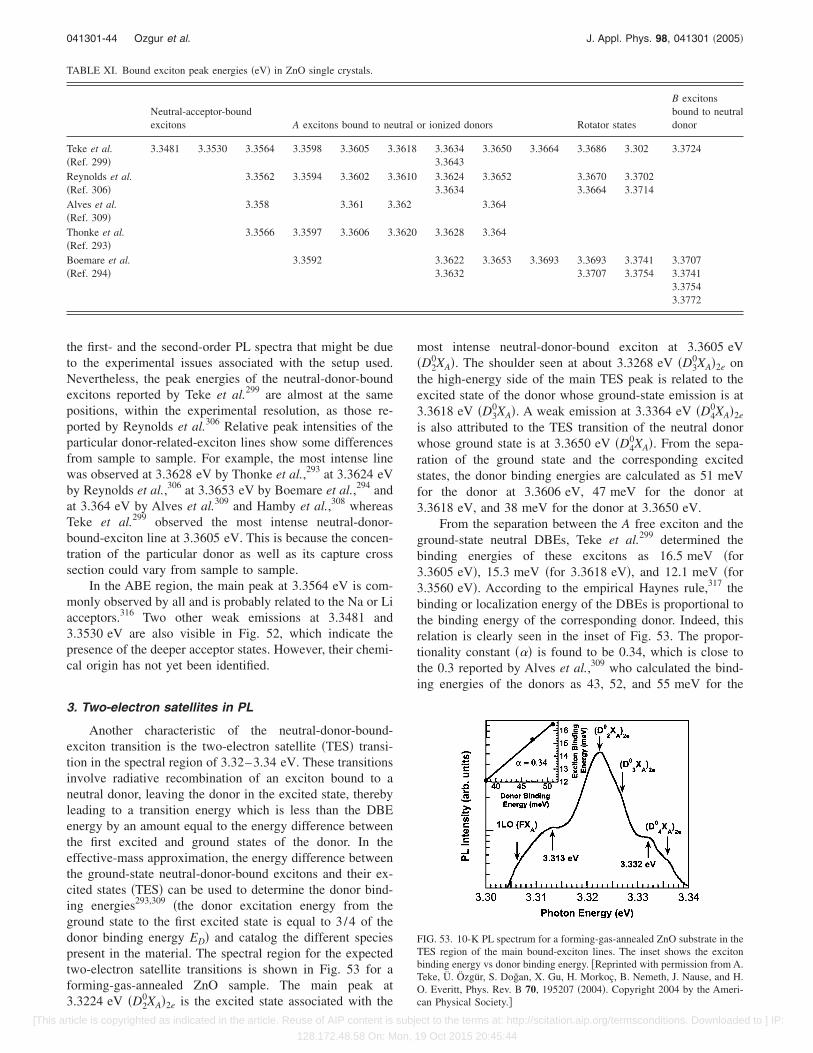
the first- and the second-order PL spectra that might be dueto the experimental issues associated with the setup used.Nevertheless, the peak energies of the neutral-donor-boundexcitons reported by Teke et al.299 are almost at the samepositions, within the experimental resolution, as those re-ported by Reynolds et al.306 Relative peak intensities of theparticular donor-related-exciton lines show some differencesfrom sample to sample. For example, the most intense linewas observed at 3.3628 eV by Thonke et al.,293 at 3.3624 eVby Reynolds et al.,306 at 3.3653 eV by Boemare et al.,294 andat 3.364 eV by Alves et al.309 and Hamby et al.,308 whereasTeke et al.299 observed the most intense neutral-donor-bound-exciton line at 3.3605 eV. This is because the concen-tration of the particular donor as well as its capture crosssection could vary from sample to sample.
In the ABE region, the main peak at 3.3564 eV is com-monly observed by all and is probably related to the Na or Liacceptors.316 Two other weak emissions at 3.3481 and3.3530 eV are also visible in Fig. 52, which indicate thepresence of the deeper acceptor states. However, their chemi-cal origin has not yet been identified.
3. Two-electron satellites in PL
Another characteristic of the neutral-donor-bound-exciton transition is the two-electron satellite �TES� transi-tion in the spectral region of 3.32–3.34 eV. These transitionsinvolve radiative recombination of an exciton bound to aneutral donor, leaving the donor in the excited state, therebyleading to a transition energy which is less than the DBEenergy by an amount equal to the energy difference betweenthe first excited and ground states of the donor. In theeffective-mass approximation, the energy difference betweenthe ground-state neutral-donor-bound excitons and their ex-cited states �TES� can be used to determine the donor bind-ing energies293,309 �the donor excitation energy from theground state to the first excited state is equal to 3/4 of thedonor binding energy ED� and catalog the different speciespresent in the material. The spectral region for the expectedtwo-electron satellite transitions is shown in Fig. 53 for aforming-gas-annealed ZnO sample. The main peak at3.3224 eV �D2
0XA�2e is the excited state associated with the
most intense neutral-donor-bound exciton at 3.3605 eV�D2
0XA�. The shoulder seen at about 3.3268 eV �D30XA�2e on
the high-energy side of the main TES peak is related to theexcited state of the donor whose ground-state emission is at3.3618 eV �D3
0XA�. A weak emission at 3.3364 eV �D40XA�2e
is also attributed to the TES transition of the neutral donorwhose ground state is at 3.3650 eV �D4
0XA�. From the sepa-ration of the ground state and the corresponding excitedstates, the donor binding energies are calculated as 51 meVfor the donor at 3.3606 eV, 47 meV for the donor at3.3618 eV, and 38 meV for the donor at 3.3650 eV.
From the separation between the A free exciton and theground-state neutral DBEs, Teke et al.299 determined thebinding energies of these excitons as 16.5 meV �for3.3605 eV�, 15.3 meV �for 3.3618 eV�, and 12.1 meV �for3.3560 eV�. According to the empirical Haynes rule,317 thebinding or localization energy of the DBEs is proportional tothe binding energy of the corresponding donor. Indeed, thisrelation is clearly seen in the inset of Fig. 53. The propor-tionality constant ��� is found to be 0.34, which is close tothe 0.3 reported by Alves et al.,309 who calculated the bind-ing energies of the donors as 43, 52, and 55 meV for the
TABLE XI. Bound exciton peak energies �eV� in ZnO single crystals.
Neutral-acceptor-boundexcitons A excitons bound to neutral or ionized donors Rotator states
B excitonsbound to neutraldonor
Teke et al.�Ref. 299�
3.3481 3.3530 3.3564 3.3598 3.3605 3.3618 3.36343.3643
3.3650 3.3664 3.3686 3.302 3.3724
Reynolds et al.�Ref. 306�
3.3562 3.3594 3.3602 3.3610 3.36243.3634
3.3652 3.36703.3664
3.37023.3714
Alves et al.�Ref. 309�
3.358 3.361 3.362 3.364
Thonke et al.�Ref. 293�
3.3566 3.3597 3.3606 3.3620 3.3628 3.364
Boemare et al.�Ref. 294�
3.3592 3.36223.3632
3.3653 3.3693 3.36933.3707
3.37413.3754
3.37073.37413.37543.3772
FIG. 53. 10-K PL spectrum for a forming-gas-annealed ZnO substrate in theTES region of the main bound-exciton lines. The inset shows the excitonbinding energy vs donor binding energy. �Reprinted with permission from A.Teke, Ü. Özgür, S. Doğan, X. Gu, H. Morkoç, B. Nemeth, J. Nause, and H.O. Everitt, Phys. Rev. B 70, 195207 �2004�. Copyright 2004 by the Ameri-can Physical Society.�
041301-44 Ozgur et al. J. Appl. Phys. 98, 041301 �2005�
[This article is copyrighted as indicated in the article. Reuse of AIP content is subject to the terms at: http://scitation.aip.org/termsconditions. Downloaded to ] IP:
128.172.48.58 On: Mon, 19 Oct 2015 20:45:44

donors whose ground-state bound-exciton lines were at3.364, 3.362, and 3.361 eV, respectively. Thonke et al.293
also studied the TES transitions and found the binding ener-gies of two shallow donors to be 39.9 and 55.5 meV. Rey-nolds et al.306 reported binding energies of 55.5 and56.7 meV for two donors at 3.3636 and 3.3614 eV, respec-tively. The Haynes proportionality constant obtained fromthese binding energies is about 2, much higher than the val-ues given above. There are two additional peaks at 3.332 and3.312 eV on both sides of the main TES lines, which couldnot be identified at this point but they may be related to theexcitons bound to structural defects.
4. DAP and LO-phonon replicas in PL
The spectral region containing the DAP transition andLO-phonon replicas of the main transitions has not beenstudied widely for single-crystal ZnO. Figure 54 shows thecorresponding spectrum taken by Teke et al.299 at 10 K for aforming-gas-treated sample. It should be noted that LO-phonon replicas occur with a separation of 71–73 meV, theLO-phonon energy in ZnO.318 Since some of the peaks areeither very weak or mixed with other closely spaced peaks,temperature evolution of these peaks should be tracked care-fully in order to make sure that the corresponding assign-ments are correct. As indicated in Fig. 54, the bump at thehigher-energy side of the spectrum labeled as 1LO �FXA� hasa peak around 3.306 eV, which is at the expected position forthe 1LO-phonon replica of the free-exciton peak �about71 meV apart from the FXA
n=1 free-exciton peak�. Althoughthey are weak, second- and third-order LO-phonon replicas�labeled as 2LO �FXA� and 3LO �FXA�� are also observed inthe PL spectrum.
The first-order LO-phonon replicas of the main neutral-bound excitons should fall between 3.290 and 3.295 eV.However, due to the line broadening, the peaks correspond-ing to each individual bound exciton could not be resolvedvery well. Indeed, the peak labeled as 1LO �D0X� has a line-width of about 6 meV, which prevents a definitive resolu-
tion. The LO-phonon replicas of the peak at 3.3650 eV canbe separated from the two other closely spaced peaks at3.3618 and 3.3605 eV. The peak at 3.2898 eV is the firstLO-phonon replica of both the 3.3618- and 3.3605-eV lines,whereas the first LO-phonon replica of the 3.3650-eV line isseen as a shoulder on the high-energy side of this intensepeak. Resolving the second- and higher-order LO replicas iseven harder because the energy position �3.218–3.223 eV�falls in the spectral region where the DAP transition and itsLO-phonon replicas are expected to appear in the PL spectra.In fact, Teke et al.299 observed a radiative recombinationpeak at 3.217 eV that is attributed to the donor-acceptor-pair�labeled as DAP in Fig. 54� transition, along with its first,second, and third LO-phonon replicas at 3.145, 3.073, and3.001 eV, respectively. Regarding the origin of the emissionline at 3.2898 eV, Reynolds et al.302 suggested that this lineis associated with an acceptor-related transition based ontheir internal strain study by changing the postannealing tem-peratures, which disagrees with the interpretation by Teke etal.299 Although the latter investigation differs somewhat, itreports at least two closely spaced peaks at 3.2898 and3.2920 eV, which are about 72 meV apart from the mainneutral-DBE lines at 3.3605 and 3.3650 eV. Thetemperature-dependent measurements also show that relativeintensities of these LO-phonon replicas follow those of themain bound excitons. Additionally, LO-phonons replicas areexpected to be roughly two orders of magnitude less intensethan the neutral-donor-bound-exciton lines.293 This is alsosimilar to the case of GaN and other II-VI semiconductors,where donor-related bound-exciton lines couple only weaklywith the optical phonons.
The relatively broad peak around 3.280 eV in Fig. 54 isthe first LO-phonon replica associated with the most intenseacceptor-bound-exciton line �3.3564 eV�. This is indicated as1LO �A0X� in the spectrum. Finally, the first-, second-, andthird-order LO-phonon replicas of the TES lines are alsoclearly observed in the PL spectra. These peaks are labeledas 1LO, 2LO, and 3LO �TES� and they are positioned at3.252, 3.182, and 3.112 eV, respectively.
5. Temperature-dependent PL measurements
In order to provide additional support for some of thepeak assignments in the low-temperature PL spectrum of thehigh-quality ZnO substrate investigated, Teke et al.299 stud-ied the temperature evolution of these peaks. Thetemperature-dependent measurements were performed be-tween 10 and 300 K. Figure 55 shows only the PL spectrafor temperatures up to 160 K because most of the importantchanges occur in this range. The spectrum for each tempera-ture is displaced vertically for clarification.
The variation of both A- and B-exciton peak positionswith temperature is shown in the inset of Fig. 55. The A- andB-exciton peaks can be tracked up to �160 K, above whichline broadening prevents a satisfactory distinction betweenthe two. This is clearly seen for the room-temperature PLspectrum, where the peak position is at �3.28 eV instead ofthe expected position of 3.31 eV �if the mostly acceptedband gap of 3.37 eV �Ref. 158� and the measured bindingenergy of 60 meV were used�. As the temperature is in-
FIG. 54. 10-K PL spectrum for a forming-gas-annealed ZnO substrate in theregion where the donor-acceptor-pair transition and LO-phonon replicas areexpected to appear. �Reprinted with permission from A. Teke, Ü. Özgür, S.Doğan, X. Gu, H. Morkoç, B. Nemeth, J. Nause, and H. O. Everitt, Phys.Rev. B 70, 195207 �2004�. Copyright 2004 by the American PhysicalSociety.�
041301-45 Ozgur et al. J. Appl. Phys. 98, 041301 �2005�
[This article is copyrighted as indicated in the article. Reuse of AIP content is subject to the terms at: http://scitation.aip.org/termsconditions. Downloaded to ] IP:
128.172.48.58 On: Mon, 19 Oct 2015 20:45:44

creased, the convergence of the A and B excitons, and thecoupling of the 1LO-phonon replica with the line broadeningof each of these peaks hamper an accurate determination ofthe peak positions above 160 K. Therefore, the room-temperature peak should be considered a combination ofthese multiple peaks.
The intensity of A and B free excitons increases withtemperature up to 40 and 80 K, respectively, and thendecreases as the temperature is increased further. From thisobservation, Teke et al.299 attribute the 3.3771- and3.3898-eV emission lines at 10 K to the free excitons corre-sponding to the A and B bands, respectively. The most in-tense acceptor-bound-exciton peak at 3.3564 eV �A1
0XA�, aswell as the other two weak acceptor-related peaks labeled as�A2
0XA� and �A30XA�, quenches gradually with increasing tem-
perature and disappears above 40 K. The temperature evolu-tion of the main neutral-donor-bound excitons was alsotraced within the temperature range of 10–160 K �see alsothe Fig. 55 inset�. With increasing temperature, the mainpeaks related to �D2
0XA� at 3.3605 eV and its TES along withtheir LO-phonon replicas quench. On the other hand, relativeintensities of the bound-exciton emissions lying between thismain DBE peak and the A-free-exciton peak increase ini-tially, where the strength depends on the particular boundexciton, and then decrease at higher temperatures. The inten-sity of the bound-exciton peak at 3.3724 eV, which was at-tributed to the B exciton bound to the main donor rather thanto a rotator state, follows the temperature behavior of the Bexciton up to 40 K, supporting the assignment of Teke etal.299 Although the B-free-exciton emission continues to in-crease up to 80 K, further increase of the donor-boundB-exciton intensity is prevented due to its partial dissociationabove 40 K. The observed temperature characteristics of thefree exciton and dominant bound exciton, where the relativeintensity IFX/ IBX is seen to increase with increasing tempera-ture, can be interpreted using the approach of Viswanath etal.319 for the study of GaN. Those authors also observed an
increase consistent with the aforementioned ratio and in-ferred that with increasing temperature the dominant donor-bound exciton dissociates into a free exciton and a neutraldonor. Based on this argument and the works of Reynolds etal.306 and Hamby et al.,308 Teke et al.299 concluded that ther-mal dissociation of the 3.3605-eV bound exciton results inincrease of the free excitons and the other shallower donor-bound excitons.
There is some controversy in the assignment of the3.223-eV peak, which is close to the main DAP transition atlow temperatures. Analyzing its temperature dependence,Thonke et al.293 attributed this peak to the free-electron-acceptor �e ,A0� transition due to thermal ionization of thedonor with increasing temperature. With the help of Hallmeasurements, they determined the acceptor ionization en-ergy to be �195 meV for the unintentional acceptor presentin ZnO, the chemical origin of which was assumed to be thesubstitutional nitrogen on O sites. On the other hand, Hambyet al.308 attributed this peak to the second LO-phonon replicaof the A free exciton. Hamby et al. observed a very goodagreement in terms of the temperature-dependent energy po-sitions of this peak with that of the predicted values by tak-ing into account the temperature broadening effect. Teke etal.299 also assigned this peak to the 2LO-phonon replica ofthe A free exciton depending on its temperature evolution. Asseen in Fig. 55, the main DAP line and its LO-phonon rep-licas quench with increasing temperature, while the adjacentline at 3.223 eV on the high-energy side increases and be-comes more apparent at higher temperatures. The tempera-ture dependence of this peak is similar to the A free exciton;it increases with increasing temperature up to 60 K and thendecreases at higher temperatures. Also, by following the ap-proach of Hamby et al.,308 the variation of A free exciton andits 1LO and 2LO peak energies with temperature are plottedin Fig. 56. As seen in this figure, the expected and measuredenergy peak positions of the 1LO and 2LO replicas of the Afree exciton agree well, supporting the assignments on these
FIG. 55. Temperature-dependent PL spectrum for a forming-gas-annealedZnO substrate. The inset shows the PL in the DAP and LO-phonon replicaregions up to 160 K. The spectrum for each temperature is displaced verti-cally for clarity. The room-temperature PL data are also included at thebottom. The lines drawn on some peaks are for guidance. �Reprinted withpermission from A. Teke, Ü. Özgür, S. Doğan, X. Gu, H. Morkoç, B. Nem-eth, J. Nause, and H. O. Everitt, Phys. Rev. B 70, 195207 �2004�. Copyright2004 by the American Physical Society.�
FIG. 56. Temperature-dependent peak positions of the A-free exciton,FXA
n=1��5� and its 1LO- and 2LO-phonon replicas. Also shown are the tem-perature evolutions of the peak positions of the two major neutral-donorbound exciton transitions at 3.3606 and 3.3650 eV. The FXA
n=1��5� data werefitted using the Varshni equation and the LO-phonon replicas were fittedwith the equation shown on the figure. �Reprinted with permission from A.Teke, Ü. Özgür, S. Doğan, X. Gu, H. Morkoç, B. Nemeth, J. Nause, and H.O. Everitt, Phys. Rev. B 70, 195207 �2004�. Copyright 2004 by the Ameri-can Physical Society.�
041301-46 Ozgur et al. J. Appl. Phys. 98, 041301 �2005�
[This article is copyrighted as indicated in the article. Reuse of AIP content is subject to the terms at: http://scitation.aip.org/termsconditions. Downloaded to ] IP:
128.172.48.58 On: Mon, 19 Oct 2015 20:45:44

peaks. It is also noted that the temperature variation of theA-free-exciton peak energy follows the Varshni formula318
Eg�T�=Eg�0�−�T2 / �T+��, where Eg�0� is the transition en-ergy at 0 K, T is the temperature, and � and � are the tem-perature coefficients. In Fig. 56, a higher-order LO-phononreplica of the A free exciton also develops persistently withincreasing temperature.
C. Time-resolved PL on ZnO
Time-resolved PL �TRPL� is a nondestructive and pow-erful technique commonly used for the optical characteriza-tion of semiconductors. The free-carrier or exciton lifetime,an important parameter related to material quality and deviceperformance, can be measured by TRPL spectroscopy. Theexciton lifetimes will vary with crystal quality, becominglonger as the quality improves. The efficiency of the radia-tive recombination is strongly related to the decay time ofthe particular transition.
Reynolds et al.320 measured the recombination lifetimeof the allowed ��5� and forbidden ��6, allowed by inducedstrain� free excitons at 2 K in a strained single-crystal ZnOgrown by the hydrothermal method as 259 and 245 ps, re-spectively. The lifetime for the �5 exciton was slightlyhigher, 322 ps, for an unstrained sample. They noted thatfree-exciton lifetimes are determined not only by the radia-tive decay but also by the nonradiative decay and by captureprocesses leading to bound excitons.321 Evidently, the mea-sured single exponential decays reflect the effects from allthree.
Teke et al.299 measured the room-temperature TRPLfrom bulk ZnO samples, one as received from Cermet, Inc.,and the other annealed in forming gas �FG�. Figure 57 showsthe TRPL data for both samples at an excitation energy den-sity of 540 �J /cm2. The time-resolved signals were inte-grated over a 10-nm-wide spectral region around the peak PLenergy �3.266 eV�. The instrument-limited rise implies thatthe relaxation processes to cool the carriers from 3.81-eVexcitation-energy-defined states to the zero-momentum exci-tonic band-edge states are very fast. For both samples, thedecaying part of the TRPL data was well described by abiexponential decay function: A1 exp�−t /�1�+A2 exp�−t /�2�.Table XII summarizes the decay constants and the amplituderatios obtained from the fits.
The fast decay constant �1 is smaller for the as-receivedsample �170.4 ps�, and most probably represents the effec-tive nonradiative recombination at room temperature. Theslow decaying component is attributed to the radiative life-time of the free exciton. The 0.86-ns value measured for theas-received sample is reasonably consistent with the0.97-ns value measured by Koida et al.322 for single-crystalZnO. The relative magnitude of the slow decaying compo-nent to the fast decaying component �A2 /A1=0.094 for540 �J /cm2� for the as-received sample suggests that thenonradiative processes are dominant. It has been proposedthat the nonradiative recombination processes are governedby the defects introduced by the Zn vacancy complexes.322
After forming-gas annealing the decay constants increasedremarkably ��1=0.86 ns and �2=2.47 ns�, and the slow de-caying component became dominant �A2 /A1=2.54 for540 �J /cm2�, suggesting an increase in radiative recombina-tion. This is also supported by the fact that the PL intensityincreased by almost a factor of 4 in the forming-gas-annealedZnO sample compared to the as-received one. The increasein the decay times is clearly observed in Fig. 57.
When the excitation density was decreased from540 to 54 �J /cm2, Teke et al.299 observed a blueshift in thePL peak by 15 meV, most probably due to reducing strengthof the band-gap renormalization. For the as-received samplethe decay constants increase slightly with increasing excita-tion density, whereas the forming-gas-treated sample followsan opposite trend. In addition, compared to the forming-gas-treated sample, the as-received sample shows a more evidentincrease in the relative strength of the slow decaying com-ponent as the excitation density is increased, as the nonradi-ative centers begin to saturate.
FIG. 57. Room-temperature time-resolved PL data for the as-received andthe forming-gas-treated samples. �Reprinted with permission from A. Teke,Ü. Özgür, S. Doğan, X. Gu, H. Morkoç, B. Nemeth, J. Nause, and H. O.Everitt, Phys. Rev. B 70, 195207 �2004�. Copyright 2004 by the AmericanPhysical Society.�
TABLE XII. TRPL decay time constants and amplitude ratios for the ZnO samples at two different excitationenergy densities. FX and DBE denote the free and donor-bound excitons, respectively �Teke et al. �Ref. 299��.
Samples
540 �J /cm2 54 �J /cm2
�1 �ps� �2 �ps� A2 /A1 �1 �ps� �2 �ps� A2 /A1
300 K As-received 170.4±1.8 863.9±14.8 0.094 116.5±1.5 585.0±6.4 0.060�FX� FG-annealed 358.7±8.8 2469±256 2.536 428.3±32.1 2969±115 2.47685 K As-received 310.2±2.5 1130±6.6 0.653 286.8±2.9 1000±5.9 0.820
�DBE� FG-annealed 474.0±5.5 1285±14.6 0.614 366.4±4.1 1021±7.3 0.869
041301-47 Ozgur et al. J. Appl. Phys. 98, 041301 �2005�
[This article is copyrighted as indicated in the article. Reuse of AIP content is subject to the terms at: http://scitation.aip.org/termsconditions. Downloaded to ] IP:
128.172.48.58 On: Mon, 19 Oct 2015 20:45:44

The decay time constants of both as-received andforming-gas-annealed samples were also measured at85 K.299 At this temperature, the main donor-bound excitonstill dominates the overall cw-PL spectrum even though Aand B free excitons are clearly observed. However, a distinc-tion between the bound and the free excitons could not bemade in the TRPL measurements due to the resolution limi-tation of the experimental setup. Therefore, the TRPL datareflect mainly the decay due to the main donor-bound exci-ton. In order to measure purely the free-excitonic-emissiondecay time, the measurements had to be performed at tem-peratures above 160 K where the bound-exciton emissiondiminishes. The time constants measured at 85 K are alsoincluded in Table XII for two different excitation densities.The main DBE-emission lines in both samples are similar interms of their intensities as observed from the time-integrated and the cw PL. Compared to the as-receivedsample, the forming-gas-annealed sample showed slightlylarger decay constants. Additionally, the decay times de-creased with decreasing excitation energy density. In contrastto the significant improvement in free-exciton lifetimes mea-sured at room temperature, the postgrowth treatment is notobserved to have a strong effect on the DBE decay times.
Epitaxial ZnO layers exhibit shorter carrier lifetimes,since they suffer from higher defect densities compared tothe bulk samples. Koida et al.322 studied the correlation be-tween the excitonic PL lifetime at room temperature andpoint defect density in bulk and epitaxial ZnO layers. Thedefect density, Zn vacancy being the most probable defect,was analyzed by positron annihilation. The single-crystalsample showed biexponential behavior with decay constantsof 0.97 and 14 ns, which were suggested to represent thefree-exciton lifetime and the free-carrier lifetime includingtrapping and emission processes, respectively. For ZnO epi-taxial layers grown by laser MBE on ScAlMgO4 �SCAM�substrates, the single exponential TRPL decay time, which ismainly governed by nonradiative processes, increased from46 to 110 ps with increasing growth temperature from570 to 800 °C. However, since a homoepitaxial film exhib-ited the shortest decay time �36 ps� in spite of the smallestnumber of point defects among the epilayers, i.e., no clearcorrelation was found between the PL decay time and thepoint defect density, the nonradiative process was consideredto be governed by certain defect species introduced by thepresence of Zn vacancies such as vacancy complexes.
Jung et al.323 reported a biexponential decay for high-quality ZnO epitaxial layers grown on sapphire by low-pressure metal-organic vapor-phase epitaxy. Room-temperature TRPL measurements produced decay times of180 ps and 1 ns, most probably representing the nonradiativeand the radiative excitonic recombination times, respectively,consistent with the measurements of Teke et al.299 and Koidaet al.322 on bulk ZnO samples.
D. Refractive index of ZnO
Knowledge of the dispersion of the refractive indices ofsemiconductor materials is necessary for accurate modelingand design of devices. The wurtzite ZnO lacks cubic sym-
metry and therefore has anisotropic optical properties. Theanisotropy results in uniaxial birefringence, two different re-fractive indices for polarization parallel �no, ordinary� andperpendicular �ne, extraordinary� to the c axis. In this sectiona summary of reported results on ZnO dielectric constantsand refractive index dispersion will be given.
In the early 1950s and 1960s, several workers reportedthe results of optical reflection measurements with light po-larized parallel and perpendicular to the c axis, and used theKramers-Kronig analysis to determine the dielectric func-tions. Mollwo16 and Bond17 have reported on refractive in-dex dispersion of single-crystal ZnO using the method ofminimum deviation at room temperature for the visible andnear-infrared spectrum. Prisms fabricated from vapor-transport-grown ZnO were used. For light below the directband edge, traditional angle-of-minimum deviation methodsproduced very accurate values of the refractive index forboth E�c and E �c. Park and Schneider24 then extended themeasurements to the spectral region near the onset of theexciton absorption at temperatures down to liquid-heliumtemperature using transmission interferometry. A ZnO plate-let sample �with the c axis lying in the plane of the platelet�grown by vapor-phase transport was used for the measure-ments. By lowering the temperature, the dispersion curveswere observed to get sharper and blueshift. The refractiveindices obtained at 4.2 K near the absorption edge are listedin Table XIII. Freeouf20 obtained the dielectric functionsabove and below the band gap by measuring the reflectivityfrom 0.6 to 30 eV before applying the Kramers-Kroniganalysis to determine the dielectric functions. Matz andLütz324 determined the optical functions of ZnO using null-ing ellipsometry at several wavelengths defined by interfer-ence filters.
Hu et al.325 used optical transmission to measure theoptical functions of thin-film ZnO prepared by pulsed-laserdeposition on �-SiO2 substrates. The ordinary refractive in-dices deduced from transmittance oscillations were 0.02–0.03 lower than the bulk ZnO crystal data by Bond.17 Theexistence of grain boundaries in the films was assumed to bethe source for this difference. Additionally, the measurementtechnique introduced a considerably large error resulting inlarge variations in the data. The best fits for the ordinaryindex using the three-term Cauchy equation
n�� = A +B
2 +C
4 , �19�
produced parameters of A=1.9281, B=−1.1157�10−5 �m2,and C=5.9696�10−3 �m4, whereas the bulk ZnO crystal17
was best characterized by A=1.9436, B=−1.9714�10−5 �m2, and C=7.0918�10−3 �m4.
The Kramers-Kronig technique is far less accurate thanthe ellipsometric technique, since it relies on less-accuratedata �reflectance� and requires extrapolations to perform theKramers-Kronig integrals. More recent measurements ofcomplex dielectric functions were reported by Yoshikawaand Adachi326 using spectroscopic ellipsometry in the photonenergy range of 1.5–5.0 eV at room temperature. Samples
041301-48 Ozgur et al. J. Appl. Phys. 98, 041301 �2005�
[This article is copyrighted as indicated in the article. Reuse of AIP content is subject to the terms at: http://scitation.aip.org/termsconditions. Downloaded to ] IP:
128.172.48.58 On: Mon, 19 Oct 2015 20:45:44
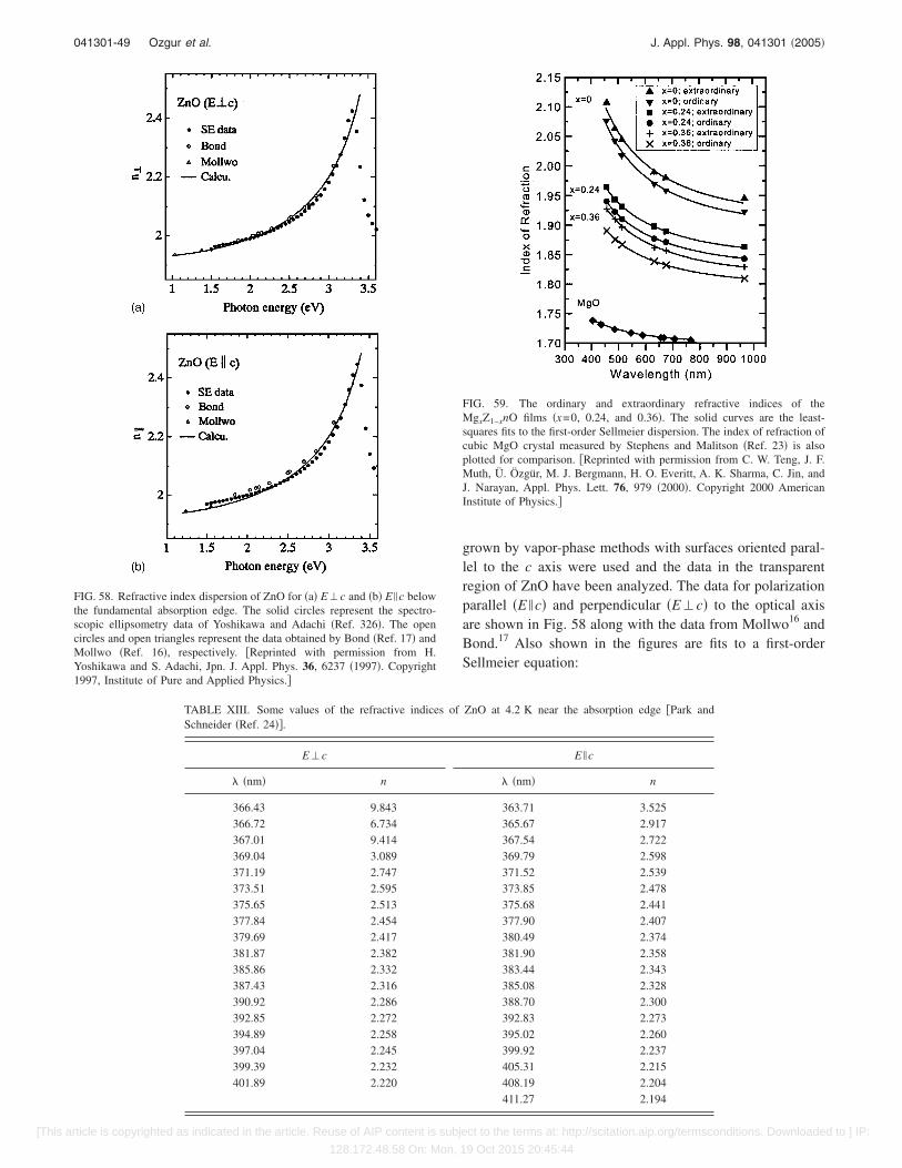
grown by vapor-phase methods with surfaces oriented paral-lel to the c axis were used and the data in the transparentregion of ZnO have been analyzed. The data for polarizationparallel �E �c� and perpendicular �E�c� to the optical axisare shown in Fig. 58 along with the data from Mollwo16 andBond.17 Also shown in the figures are fits to a first-orderSellmeier equation:
FIG. 58. Refractive index dispersion of ZnO for �a� E�c and �b� E �c belowthe fundamental absorption edge. The solid circles represent the spectro-scopic ellipsometry data of Yoshikawa and Adachi �Ref. 326�. The opencircles and open triangles represent the data obtained by Bond �Ref. 17� andMollwo �Ref. 16�, respectively. �Reprinted with permission from H.Yoshikawa and S. Adachi, Jpn. J. Appl. Phys. 36, 6237 �1997�. Copyright1997, Institute of Pure and Applied Physics.�
FIG. 59. The ordinary and extraordinary refractive indices of theMgxZ1−xnO films �x=0, 0.24, and 0.36�. The solid curves are the least-squares fits to the first-order Sellmeier dispersion. The index of refraction ofcubic MgO crystal measured by Stephens and Malitson �Ref. 23� is alsoplotted for comparison. �Reprinted with permission from C. W. Teng, J. F.Muth, Ü. Özgür, M. J. Bergmann, H. O. Everitt, A. K. Sharma, C. Jin, andJ. Narayan, Appl. Phys. Lett. 76, 979 �2000�. Copyright 2000 AmericanInstitute of Physics.�
TABLE XIII. Some values of the refractive indices of ZnO at 4.2 K near the absorption edge �Park andSchneider �Ref. 24��.
E�c E �c
�nm� n �nm� n
366.43 9.843 363.71 3.525366.72 6.734 365.67 2.917367.01 9.414 367.54 2.722369.04 3.089 369.79 2.598371.19 2.747 371.52 2.539373.51 2.595 373.85 2.478375.65 2.513 375.68 2.441377.84 2.454 377.90 2.407379.69 2.417 380.49 2.374381.87 2.382 381.90 2.358385.86 2.332 383.44 2.343387.43 2.316 385.08 2.328390.92 2.286 388.70 2.300392.85 2.272 392.83 2.273394.89 2.258 395.02 2.260397.04 2.245 399.92 2.237399.39 2.232 405.31 2.215401.89 2.220 408.19 2.204
411.27 2.194
041301-49 Ozgur et al. J. Appl. Phys. 98, 041301 �2005�
[This article is copyrighted as indicated in the article. Reuse of AIP content is subject to the terms at: http://scitation.aip.org/termsconditions. Downloaded to ] IP:
128.172.48.58 On: Mon, 19 Oct 2015 20:45:44

n��2 = A +B2
2 − C2 , �20�
where A, B, and C are the fitting parameters, and is thewavelength. Best fits were obtained for A=2.84, B=0.84,and C=0.319 �m for E�c, and A=2.85, B=0.87, and C=0.310 �m for E �c.
Jellison and Boatner327 employed a two-modulator gen-eralized ellipsometry �2-MGE� technique to determine theanisotropic optical functions of ZnO, using samples grownby chemical-vapor transport and hydrothermal methods.Near and above the band edge, the resulting dielectric func-tions from both samples were identical within the experi-mental error, whereas the refractive indices of hehydrothermal-grown sample were �0.012±0.007 smallerthan the refractive index of the vapor-transport-grownsample from 850 to 450 nm. 2-MGE is claimed to producethe most accurate results above the band edge, particularlymore accurate than the results by Freeouf20 in the measuredspectral region of 3.3–5.0 eV, while the refractive indicesdetermined below the direct band edge agree with theminimum-deviation methods17 within an accuracy of ±0.003.
Using the prism-coupled waveguide technique, Teng etal.328 measured the indices of refraction for MgxZn1−xO epi-taxial films grown on c-plane sapphire substrates by pulsed-laser deposition. Measurements were performed for sampleswith x up to 0.36 in the wavelength range of 457–968 nm.The results are shown in Fig. 59 for the ordinary and theextraordinary refractive indices. The data were fit by theleast-squares method to the first-order Sellmeier dispersionrelationship with A=1 in Eq. �20�. The data for the ZnOsample were best characterized with fitting parameters B=2.60±0.02 and C=0.2114±0.0037 �m for the ordinary in-dex and B=2.66±0.02 and C=0.2143±0.0051 �m for theextraordinary index. The Sellmeier parameters forMgxZn1−xO films are summarized in Table XIV.
One of the most recent reports of dielectric functions ofZnO is by Ashkenov et al.118 who characterized thin films
grown by pulsed-laser deposition on c-plane sapphire and asingle-crystalline sample grown by seeded chemical-vaportransport method. The static dielectric constant was obtainedfrom infrared spectroscopic ellipsometry measurements. Thehigh-frequency dielectric constant was calculated throughthe Lyddane-Sachs-Teller �LST� relation using the static con-stant and the TO- and LO-phonon mode frequencies. Theresults are compared with the data from some of the previousreports in Table XV.
Schmidt et al.329 also reported room-temperature spec-troscopic ellipsometry results on pulsed-laser-deposition-grown wurtzite MgxZn1−xO �0�x�0.29� thin films. The re-fractive index data were fit to a three-term Cauchy-approximation-type formula �Eq. �19�� and the anisotropicCauchy model parameters A, B, and C for ZnO were ob-tained as 1.916, 1.76, and 3.9 for E�c, and 1.844, 1.81, and3.6 for E �c, respectively. For the MgxZn1−xO alloy system,linear dependence of the Cauchy parameters on x was as-sumed:
n�� = A + ax +B + bx
2 +C + cx
4 . �21�
The coefficients b and c were found isotropic, and the pa-rameters obtained from fits to Eq. �21� are listed in TableXVI. Surprisingly, for all the MgxZn1−xO thin films investi-gated the birefringence was found negative, unlike ZnO,which showed positive birefringence �0.05� in the transpar-ency region. This change of the sign of the birefringencegoing from ZnO to the MgxZn1−xO alloy system is in con-trast to the results reported by Teng et al.,328 where a positivebirefringence of approximately 0.025 for ZnO andMgxZn1−xO for all Mg contents was found. When comparedto the ZnO data by Teng et al.328 Jellison and Boatner,327
Yoshikawa and Adachi,326 and Hu et al.,325 the ZnO ordinaryand extraordinary refractive index values of Schmidt et al.329
are about 0.02 lower and 0.03 higher, respectively, up to700 nm, and the birefringence is larger.
TABLE XV. Static and high-frequency dielectric constants of ZnO.
Sample
Ashkenov et al.�Ref. 118�
Teng et al.�Ref. 328�
Yoshikawa andAdachi �Ref. 326� Bond �Ref. 17�
Thin film Bulk Thin film Bulk Bulk
�0a E�c 7.46 7.77 7.44 7.61 7.65
E �c 8.59 8.91 8.36 8.50 8.57�� E�c 3.61 3.70 3.60 3.68 3.70
E �c 3.76 3.78 3.66 3.72 3.75
aCalculated via the LST relation with the phonon mode parameters obtained by Ashkenov et al. �Ref. 118�.
TABLE XIV. Sellmeier coefficients for MgxZn1−xO films �After Teng et al. �Ref. 328��.
Parameter x=0 x=0.24 x=0.36
Ordinary index B 2.60±0.02 2.37±0.003 2.27±0.004E�c C ��m� 0.2114±0.0037 0.1793±0.0012 0.1686±0.0008Extraordinary index B 2.66±0.02 2.43±0.01 2.32±0.01E �c C ��m� 0.2143±0.0051 0.1815±0.0016 0.1801±0.0016
041301-50 Ozgur et al. J. Appl. Phys. 98, 041301 �2005�
[This article is copyrighted as indicated in the article. Reuse of AIP content is subject to the terms at: http://scitation.aip.org/termsconditions. Downloaded to ] IP:
128.172.48.58 On: Mon, 19 Oct 2015 20:45:44
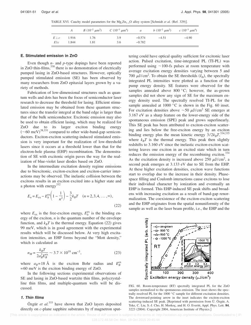
E. Stimulated emission in ZnO
Even though n- and p-type dopings have been reportedin ZnO thin-films,330 there is no demonstration of electricallypumped lasing in ZnO-based structures. However, opticallypumped stimulated emission �SE� has been observed bymany researchers from ZnO epitaxial layers grown by a va-riety of methods.
Fabrication of low-dimensional structures such as quan-tum wells and dots has been the focus of semiconductor laserresearch to decrease the threshold for lasing. Efficient stimu-lated emission may be obtained from these quantum struc-tures since the transfer integral at the band edge is larger thanthat of the bulk semiconductor. Excitonic emission may alsobe used to obtain efficient lasing, which may be realized forZnO due to its larger exciton binding energy��60 meV�38,331 compared to other wide-band-gap semicon-ductors. Exciton-exciton scattering-induced stimulated emis-sion is very important for the realization of low-thresholdlasers since it occurs at a threshold lower than that for theelectron-hole plasma �EHP� recombination. The demonstra-tion of SE with excitonic origin paves the way for the real-ization of blue-violet laser diodes based on ZnO.
In the intermediate excitation density regime emissionsdue to biexcitonic, exciton-exciton and exciton-carrier inter-actions may be observed. The inelastic collision between theexcitons results in an exciton excited into a higher state anda photon with energy332
En = Eex − Ebex1 −
1
n2 −3
2kBT �n = 2,3,4, . . . ,�� ,
�22�
where Eex is the free-exciton energy, Ebex is the binding en-
ergy of the exciton, n is the quantum number of the envelopefunction, and kBT is the thermal energy. Equation �22� gives99 meV, which is in good agreement with the experimentalresults which will be discussed below. At very high excita-tion intensities, an EHP forms beyond the “Mott density,”which is calculated as
nM =kBT
2aB3EB
ex � 3.7 � 1019 cm−3, �23�
where aB=18 Å is the exciton Bohr radius and EBex
=60 meV is the exciton binding energy of ZnO.In the following sections experimental observations of
SE and lasing in ZnO-based wurtzite thin films, polycrystal-line thin films, and multiple-quantum wells will be dis-cussed.
1. Thin films
Özgür et al.333 have shown that ZnO layers depositeddirectly on c-plane sapphire substrates by rf magnetron sput-
tering could have optical quality sufficient for excitonic laseraction. Pulsed excitation, time-integrated PL �TI-PL� wasperformed using �100-fs pulses at room temperature withaverage excitation energy densities varying between 5 and700 �J /cm2. To obtain the SE thresholds �Ith�, the spectrallyintegrated PL intensities were plotted as a function of thepump energy density. SE features were observed for thesamples annealed above 800 °C; however, the as-grownsamples did not show any sign of SE for the maximum en-ergy density used. The spectrally resolved TI-PL for thesample annealed at 1000 °C is shown in the Fig. 60 inset.For excitation densities above �50 �J /cm2 SE emerges at3.167 eV as a sharp feature on the lower-energy side of thespontaneous emission �SPE� peak and grows superlinearly.This SE peak has been attributed to exciton-exciton scatter-ing and lies below the free-exciton energy by an excitonbinding energy plus the mean kinetic energy 3/2kBT,334,335
where kBT is the thermal energy. This peak then slightlyredshifts to 3.160 eV since the inelastic exciton-exciton scat-tering leaves one exciton in an excited state which in turnreduces the emission energy of the recombining exciton.334
As the excitation density is increased above 250 �J /cm2, asecond peak emerges at 3.133 eV due to SE from the EHP.At these higher excitation densities, exciton wave functionsstart to overlap due to the increase in their density. Phase-space filling and Coulomb interactions cause excitons to losetheir individual character by ionization and eventually anEHP is formed. This EHP-induced SE peak shifts and broad-ens with increasing excitation as a result of band-gap renor-malization. The coexistence of the exciton-exciton scatteringand the EHP originates from the spatial nonuniformity of thesample as well as the laser beam profile, i.e., the EHP and the
TABLE XVI. Cauchy model parameters for the MgxZn1−xO alloy system �Schmidt et al. �Ref. 329��.
A B �10−2 �m2� C �10−3 �m4� a b �10−2 �m2� c �10−3 �m4�
E�c 1.916 1.76 3.9 −0.574 −4.51 −4.90E �c 1.844 1.81 3.6 −0.782
FIG. 60. Room-temperature �RT� spectrally integrated PL for the ZnOsamples normalized to the spontaneous emission. The inset shows the spec-trally resolved PL for the 1000 °C sample for different excitation densities.The downward-pointing arrow in the inset indicates the exciton-excitonscattering-induced SE peak. �Reprinted with permission from Ü. Özgür, A.Teke, C. Liu, S.-J. Cho, H. Morkoç, and H. O. Everitt, Appl. Phys. Lett. 84,3223 �2004�. Copyright 2004, American Institute of Physics.�
041301-51 Ozgur et al. J. Appl. Phys. 98, 041301 �2005�
[This article is copyrighted as indicated in the article. Reuse of AIP content is subject to the terms at: http://scitation.aip.org/termsconditions. Downloaded to ] IP:
128.172.48.58 On: Mon, 19 Oct 2015 20:45:44

exciton-exciton-scattering-induced SE may come from dif-ferent regions of the sample excited by the laser.
Özgür et al.333 observed the SE peak attributed toexciton-exciton scattering also for another rf-sputteredsample annealed at 950 °C, but not for the sample annealedat 800 °C. Due to the existence of exciton-exciton scattering,Ith for the 950 and 1000 °C samples �49 and 58 �J /cm2,respectively� were significantly lower than that for the800 °C sample �130 �J /cm2�. Figure 60 shows the PL dataspectrally integrated between 3.1 and 3.4 eV for all thesamples.
Stimulated emission and lasing, which could surviveeven at temperatures as high as 550 K, have been observedby Bagnall et al.335,336 in ZnO thin films grown by plasma-enhanced MBE on c-plane sapphire. At room temperature,for excitation intensities exceeding 400 kW/cm2 the exciton-exciton-scattering-related SE peak appeared at 3.18 eV andgrew superlinearly. At higher excitation intensities�800 kW/cm2� the electron-hole plasma peak appeared at3.14 eV and broadened and redshifted due to band-gaprenormalization with further increase in the excitation inten-sity. The thresholds for the SE lines were 1.2 and1.9 MW/cm2 for the exciton-exciton scattering and EHPmechanisms, respectively. Figure 61 shows the SE observedat room temperature and at 550 K.
Bagnall et al.163 reported optically pumped room-temperature lasing from cleaved ZnO cavities even throughthey were unable to observe the longitudinal cavity modesdirectly. In a later study,336 they could clearly see a verystrong and stable mode structure on the room-temperatureEHP emission peak of one of the ZnO epitaxial layers �seeFig. 62�. Although its origin was not explicitly identified, thelasing was claimed to be produced by a naturally formed or“accidental” �70-�m cavity as calculated from the 0.5-nmmode spacing. In the same samples, pump-probe measure-ments revealed that the optical gain forms when photoex-
cited hot carriers cool down to an EHP state.337 Yu et al.338
also observed optically pumped lasing in 60-nm-thick micro-crystalline ZnO films grown on c-plane sapphire by laserMBE. However, the lasing mechanism was attributed to in-elastic exciton-exciton scattering and a peak gain of300 cm−1 was observed at a fluence of 3.8 �J /cm2. Althoughdifferent optical pumping conditions could be a reason forthe observed discrepancy, the different crystal properties ofthe investigated epitaxial layers should also play a criticalrole in lasing mechanisms.
By using the variable stripe length method, Chen etal.334 measured the optical gain spectrum of ZnO epilayerswhich were grown on c-plane sapphire by plasma-assistedMBE �P-MBE� employing a thin MgO buffer layer. Figure63 shows the stimulated-emission spectra with excitationdensity near Ith for various excitation stripe lengths. Thesharp increase of the emission intensity with excitation
FIG. 61. Normalized PL spectra forvarious excitation intensities at �a�room temperature and at �b� 550 K�Reprinted with permission from D.M. Bagnall, Y. F. Chen, Z. Zhu, T.Yao, M. Y. Shen, and T. Goto, Appl.Phys. Lett. 73, 1038 �1998�. Copyright1998, American Institute of Physics.�
FIG. 62. Room-temperature laser emission spectra. The inset shows clearlythe resolved mode.s �Reprinted from D. M. Bagnall, Y. F. Chen, M. Y. Shen,Z. Zhu, T. Goto, and T. Yao, J. Cryst. Growth 184–185, 605 �1998�, Copy-right 1998, with permission from Elsevier.�
041301-52 Ozgur et al. J. Appl. Phys. 98, 041301 �2005�
[This article is copyrighted as indicated in the article. Reuse of AIP content is subject to the terms at: http://scitation.aip.org/termsconditions. Downloaded to ] IP:
128.172.48.58 On: Mon, 19 Oct 2015 20:45:44
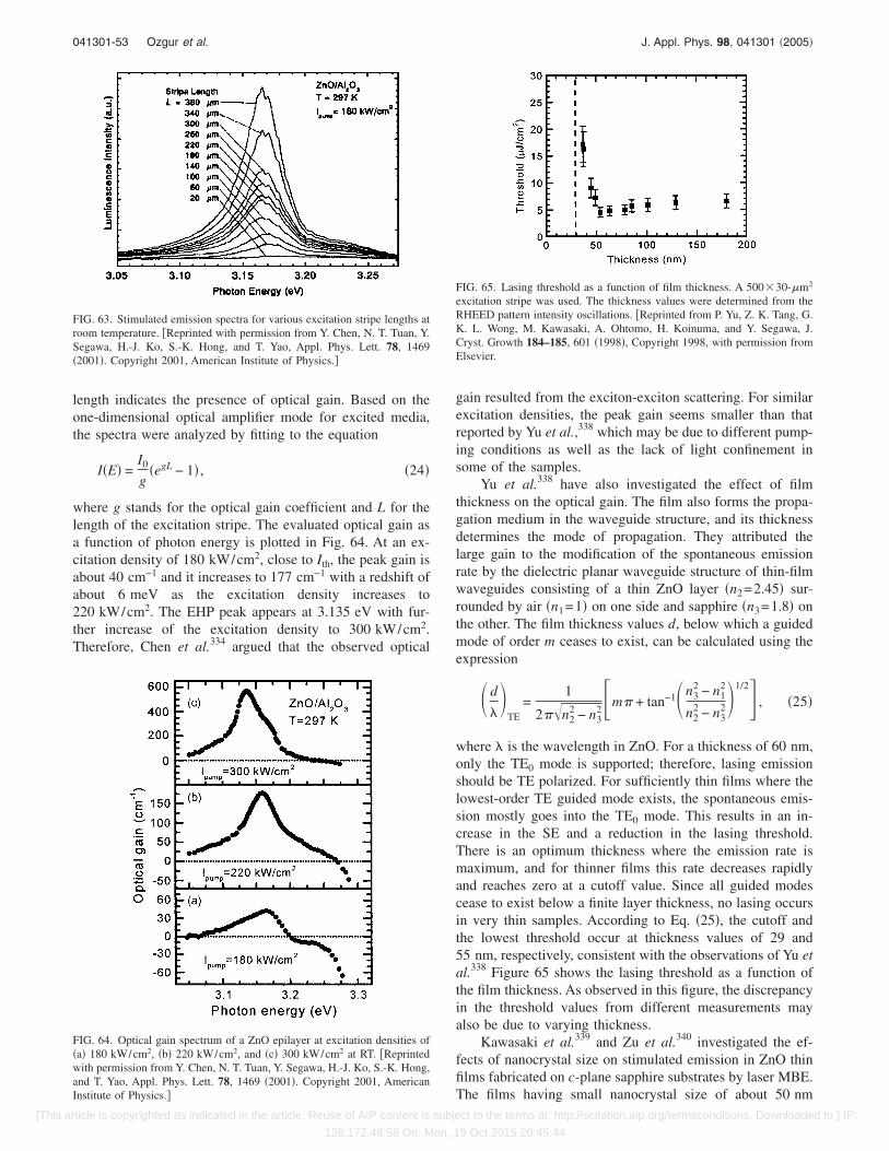
length indicates the presence of optical gain. Based on theone-dimensional optical amplifier mode for excited media,the spectra were analyzed by fitting to the equation
I�E� =I0
g�egL − 1� , �24�
where g stands for the optical gain coefficient and L for thelength of the excitation stripe. The evaluated optical gain asa function of photon energy is plotted in Fig. 64. At an ex-citation density of 180 kW/cm2, close to Ith, the peak gain isabout 40 cm−1 and it increases to 177 cm−1 with a redshift ofabout 6 meV as the excitation density increases to220 kW/cm2. The EHP peak appears at 3.135 eV with fur-ther increase of the excitation density to 300 kW/cm2.Therefore, Chen et al.334 argued that the observed optical
gain resulted from the exciton-exciton scattering. For similarexcitation densities, the peak gain seems smaller than thatreported by Yu et al.,338 which may be due to different pump-ing conditions as well as the lack of light confinement insome of the samples.
Yu et al.338 have also investigated the effect of filmthickness on the optical gain. The film also forms the propa-gation medium in the waveguide structure, and its thicknessdetermines the mode of propagation. They attributed thelarge gain to the modification of the spontaneous emissionrate by the dielectric planar waveguide structure of thin-filmwaveguides consisting of a thin ZnO layer �n2=2.45� sur-rounded by air �n1=1� on one side and sapphire �n3=1.8� onthe other. The film thickness values d, below which a guidedmode of order m ceases to exist, can be calculated using theexpression
d
TE=
1
2��n22 − n3
2�m� + tan−1n32 − n1
2
n22 − n3
21/2� , �25�
where is the wavelength in ZnO. For a thickness of 60 nm,only the TE0 mode is supported; therefore, lasing emissionshould be TE polarized. For sufficiently thin films where thelowest-order TE guided mode exists, the spontaneous emis-sion mostly goes into the TE0 mode. This results in an in-crease in the SE and a reduction in the lasing threshold.There is an optimum thickness where the emission rate ismaximum, and for thinner films this rate decreases rapidlyand reaches zero at a cutoff value. Since all guided modescease to exist below a finite layer thickness, no lasing occursin very thin samples. According to Eq. �25�, the cutoff andthe lowest threshold occur at thickness values of 29 and55 nm, respectively, consistent with the observations of Yu etal.338 Figure 65 shows the lasing threshold as a function ofthe film thickness. As observed in this figure, the discrepancyin the threshold values from different measurements mayalso be due to varying thickness.
Kawasaki et al.339 and Zu et al.340 investigated the ef-fects of nanocrystal size on stimulated emission in ZnO thinfilms fabricated on c-plane sapphire substrates by laser MBE.The films having small nanocrystal size of about 50 nm
FIG. 63. Stimulated emission spectra for various excitation stripe lengths atroom temperature. �Reprinted with permission from Y. Chen, N. T. Tuan, Y.Segawa, H.-J. Ko, S.-K. Hong, and T. Yao, Appl. Phys. Lett. 78, 1469�2001�. Copyright 2001, American Institute of Physics.�
FIG. 64. Optical gain spectrum of a ZnO epilayer at excitation densities of�a� 180 kW/cm2, �b� 220 kW/cm2, and �c� 300 kW/cm2 at RT. �Reprintedwith permission from Y. Chen, N. T. Tuan, Y. Segawa, H.-J. Ko, S.-K. Hong,and T. Yao, Appl. Phys. Lett. 78, 1469 �2001�. Copyright 2001, AmericanInstitute of Physics.�
FIG. 65. Lasing threshold as a function of film thickness. A 500�30-�m2
excitation stripe was used. The thickness values were determined from theRHEED pattern intensity oscillations. �Reprinted from P. Yu, Z. K. Tang, G.K. L. Wong, M. Kawasaki, A. Ohtomo, H. Koinuma, and Y. Segawa, J.Cryst. Growth 184–185, 601 �1998�, Copyright 1998, with permission fromElsevier.
041301-53 Ozgur et al. J. Appl. Phys. 98, 041301 �2005�
[This article is copyrighted as indicated in the article. Reuse of AIP content is subject to the terms at: http://scitation.aip.org/termsconditions. Downloaded to ] IP:
128.172.48.58 On: Mon, 19 Oct 2015 20:45:44

showed excitonic SE as well as the SE from the EHP. Thespontaneous emission generated by exciton-exciton colli-sions, which showed a quadratic intensity dependence, wasfollowed by SE from the same process at higher excitationintensities exhibiting an eighth-power dependence. With fur-ther increase of the excitation intensity the Coulomb interac-tion leads to ionization of excitons and the formation of adense EHP. Therefore, the intensity of the excitonic SE peakis observed to reduce. This was not observed in previouslymentioned reports due to the sample inhomogeneity. Anothermajor observation was that, unlike the EHP-induced SE, theexciton-exciton-scattering-induced SE was not present in thefilms having larger nanocrystal size. Kawasaki et al.339 con-cluded that there is an optimum hexagonally shaped micro-crystallite size of �50 nm�3 for observing excitonic SE. Ana-lyzing similar results, Ohtomo et al.341 speculated that theexcitonic stimulated emission is due to the giant oscillatorstrength that can occur in high-quality nanocrystals with adimension larger than the exciton Bohr radius ��2 nm�, butsmaller than the optical wavelength �390 nm�. For large-grain samples, the exciton superradiance effect becomesweak such that the exciton-exciton collision process shouldnot occur. Thus, the grain boundaries between nanocrystalsare considered to serve as barriers resulting in the confine-ment of excitons in nanocrystals.
2. Polycrystalline ZnO films and “random lasers”
As previously observed in Ti:sapphire and TiO2 disor-dered systems,342,343 there have been reports of “random las-ing” in polycrystalline ZnO films as a result of strong scat-tering in disordered dielectric media.344–346 It was shown thatin the case of such strong scattering and gain, recurring scat-tering events could provide coherent feedback and result inlasing.347 When the scattering mean free path becomes equalto or less than the wavelength, photon may return to a scat-terer from which it was scattered before, and thereby closed-loop paths may be formed. If the amplification along such aloop path exceeds the loss, lasing could occur in the loop thatserves as a resonator. Such a laser is called a “random laser,”where the phase shift along the loop must be equal to amultiple of 2�. Unlike the traditional semiconductor laserswhich have well-defined cavities, the random-laser cavitiesare “self-formed” due to strong optical scattering in the poly-crystalline films. The main requirement to observe this kindof laser emission is that the particle size should be less thanthe emission wavelength. The photon localization in this caseis similar to Anderson localization of electrons in disorderedsystems.348
Cao et al.344,345 observed random-laser emission in poly-crystalline ZnO. Figure 66 shows the evolution of the emis-sion spectra as the pump intensity was increased.345 At lowexcitation intensities, the spectrum consisted of a singlebroad spontaneous-emission peak. As the pump power in-creased, the emission peak became narrower due to the pref-erential amplification at frequencies close to the maximum ofthe gain spectrum. When the excitation intensity exceeded athreshold, very narrow peaks emerged in the emission spec-tra. The linewidth of these peaks was less than 0.3 nm, whichwas more than 30 times smaller than the linewidth of the
amplified spontaneous-emission peak below the threshold.When the pump intensity increased further, more sharp peaksappeared. The frequencies of the sharp peaks depended onthe sample position, that is, when the excitation spot wasmoved across the film, the frequencies of the sharp peakschanged. Above the threshold, the integrated emission inten-sity increased much more rapidly with the pump power, andthe emission was measured to be strongly polarized, indicat-ing that laser action has occurred in the ZnO films.
The characteristics of lasing in semiconductor polycrys-talline films exhibit remarkable differences from that of aconventional laser. First of all, the laser emission from theZnO polycrystalline films can be observed in all directions,and the laser emission spectrum varies with the observationangle. Second, the pump intensity required to reach the las-ing threshold depends on the excitation area. As the excita-tion area decreases, the lasing threshold density increases,and when the excitation area is reduced to below a criticalsize, lasing stops because the closed-loop paths are too short,and the amplification along the loops is not high enough toachieve lasing. When the excitation area is increased, morelasing peaks emerge in the emission spectra that is explainedby forming more closed-loop paths for light, and thus, in-creasing the number of lasing modes. The shape and size ofthe laser cavities change as the excitation spot is movedacross the film. The size and shape of the laser resonators aredetermined by the optical gain coefficient, the grain size and
FIG. 66. Spectra of emission from the ZnO powder when the excitationintensities are �from bottom to top� 400, 562, 763, 875, and 1387 kW/cm2.The thickness of the film of the ZnO powder is 6 �m. The excitation area isabout 1600 �m2. The inset is a schematic diagram showing the formation ofa closed-loop path for light through recurring scattering in the powder. �Re-printed with permission from H. Cao, Y. G. Zhao, S. T. Ho, E. W. Seelig, Q.H. Wang, and R. P. H. Chang, Phys. Rev. Lett. 82, 2278 �1999�. Copyright1999 by the American Physical Society.�
041301-54 Ozgur et al. J. Appl. Phys. 98, 041301 �2005�
[This article is copyrighted as indicated in the article. Reuse of AIP content is subject to the terms at: http://scitation.aip.org/termsconditions. Downloaded to ] IP:
128.172.48.58 On: Mon, 19 Oct 2015 20:45:44
distribution, the scattering cross section, and the boundaryconditions, so the lasing frequencies vary across the film.
The microlasers have potential applications in integratedphotonic circuits. The demonstration of random lasers opensup the possibility of using disordered semiconductor micro-structures as alternative sources of coherent light emission.The fabrication of the conventional microlasers requires ex-pensive state-of-the-art crystal growth and microfabricationfacilities. The realization of lasing in semiconductor poly-crystalline films, which are nonepitaxially grown on amor-phous fused silica substrates, provides a possibility to fabri-cate semiconductor lasers on many different types ofsubstrates. As a result, fabrication of such a polycrystallinefilm-based microlaser is much easier and less expensive thanthat of most microlasers. In this context development ofmethods for growing high-quality polycrystalline ZnO filmsis important, since polycrystalline ZnO films also have manyother applications as phosphors, coatings, etc., in variousdevices.349
Several authors suggested very simple methods forgrowing polycrystalline ZnO films by oxidation of metallicZn films deposited on different substrates.350–354 Dimova-Alyakova et al.350 obtained polycrystalline ZnO films by oxi-dation of metal Zn films deposited on sapphire substrates bythermal evaporation. However, the quality of the films wasquite poor as judged by the weak near-band-edge emissioneven at high excitation levels. Cho et al.351 succeeded inpreparing high-quality polycrystalline ZnO thin films havingstrong band-edge emission by oxidation of Zn films depos-ited on silica substrates by magnetron sputtering. Increasingthe oxidation temperature from 300 to 1000 °C led to an in-crease in the average grain size from 18 to 61 nm. Also as aresult, the PL peak intensity increased, FWHM decreased,and the peak position redshifted �due to quantum confine-ment effects in grains� as shown in Fig. 67. The PL FWHMswere 107 and 23 meV for the samples annealed at 700 and1000 °C, respectively. Optically pumped lasing action inthese ZnO polycrystalline films was observed with a thresh-old intensity of 9 MW/cm2 �see Fig. 68�. These results indi-cate that polycrystalline ZnO thin films prepared by thermaloxidation from metallic Zn films are suitable for fabricationof random lasers. The results reported by Chen et al.352 werealmost similar to those reported in this work.351 However,
Wang et al.353 reported the optimum oxidizing temperatureto be 410 °C at which the best crystallinity and the mostintense PL emission were observed. The authors attributedthis phenomenon to the low rate of formation of intrinsicdefects at such a low temperature.
Alivov et al.354 studied the properties �crystal, optical,and electrical� of polycrystalline ZnO films obtained by oxi-dizing metallic Zn layers which were electron-beam evapo-rated on various substrates. No predominating orientationwas observed for the Zn and ZnO films deposited on glass,sapphire, and silica. Besides, the mean grain size in Zn films�120 nm� as well as in the subsequent ZnO films �size de-pending on the oxidation temperature� was also independentof the substrate nature. A dramatic improvement of the PLwith increasing oxidation temperature was observed as inRef. 351. The effect of oxygen partial pressure was studiedrecording the RT cathodoluminescence �CL� spectra of se-lected ZnO films oxidized at T=800 °C and at different oxy-gen partial pressures. As seen from Fig. 69 the UV CL in-tensity increased by almost a factor of 10 when the oxygenpartial pressure was decreased from 760 to 5�10−5 Torr.FWHM of the UV CL band decreased from 125 to 81 meVin the same pressure range. When the annealing temperaturewas increased from 400 to 900 °C the mean grain size of thefilms increased from 138 to 245 nm, the resistivity � in-creased from 3.81�102 to 6.02�104 � cm, electron con-centration decreased from 4.56�1015 to 7.32�1012 cm−3,and mobility increased from 3.6 to 14.2 cm2/V s. The varia-
FIG. 67. PL intensity and PL peak position vs annealing temperature. �Re-printed with permission from S. Cho, J. Ma, Y. Kim, Y. Sun, G. K. L. Wong,and J. B. Ketterson, Appl. Phys. Lett. 75, 2761 �1991�. Copyright 1999,American Institute of Physics.�
FIG. 68. Lasing spectra of the polycrystalline ZnO thin film obtained byoxidation of metallic Zn films. The threshold intensity �Ith� for the lasingwas �9 MW/cm2. �Reprinted with permission from S. Cho, J. Ma, Y. Kim,Y. Sun, G. K. L. Wong, and J. B. Ketterson, Appl. Phys. Lett. 75, 2761�1999�. Copyright 1999, American Institute of Physics.�
FIG. 69. The dependences of the UV CL peak intensity and FWHM as afunction of oxygen partial pressure �T=300 K, electron-beam current of1 �A was used for excitation� �after Alivov et al. �Ref. 354��.
041301-55 Ozgur et al. J. Appl. Phys. 98, 041301 �2005�
[This article is copyrighted as indicated in the article. Reuse of AIP content is subject to the terms at: http://scitation.aip.org/termsconditions. Downloaded to ] IP:
128.172.48.58 On: Mon, 19 Oct 2015 20:45:44
tion of the electrical properties with the oxygen partial pres-sure was very small compared to the oxidation temperature.The resistivity and mobility increased only by a factor of 2-4when oxygen partial pressure was varied from 1.01�10−5 to 1.33�10−3 Pa.
3. Multiple-quantum wells
Stimulated emission has been observed also in quantum-well structures utilizing the alloys of ZnO. It is expected thatthe observation of the excitonic SE phenomenon should befavored in quantum wells owing to the enhanced bindingenergy of excitons and hence by the larger stability of theexciton states. However, in other II-VI materials SE has beenmostly demonstrated only at low temperatures and rarely atroom temperature. Ohtomo et al.355 reported the observationof SE in ZnO/ZnMgO multiple-quantum wells �MQWs� upto 373 K, but did not elucidate the mechanism of SE. Theyinvestigated ten-period MQWs grown on SCAM substratesby laser MBE. The barriers were 5 nm thick, and the widthsof the wells varied from 0.7 to 4.7 nm. The stimulated-emission threshold was observed to increase with decreasingwell width and also with increasing Mg composition in thebarriers. Figure 70 shows the variation of the SE thresholdwith well width for two sets of samples having 12% and 26%Mg in the barriers.
Sun et al.356 later investigated the mechanism of SE inthe same MQW samples. They observed SE induced by bothexciton-exciton scattering and EHP recombination. Theexciton-origined recombination mechanism of SE was stud-ied further by measuring the temperature dependence of theSE peak position. It was observed that the exciton-excitonband has the same temperature-dependence characteristics asthat of a ZnO single layer, supporting the notion that thisemission in ZnO/MgZnO MQWs is indeed due to exciton-exciton scattering. Additionally, the measurements at 5 K re-vealed that the exciton binding energy increases with de-creasing QW width. These binding energies were deducedfrom the energy difference between the exciton-exciton-scattering-related and the free-exciton emission lines.
4. Stimulated-emission dynamics
In order to investigate the effects of annealing and SE oncarrier dynamics, TRPL spectroscopy was employed at roomtemperature and at 85 K by Özgür et al.333 The TRPL mea-surements used the same optical pulse excitation source asthe TI-PL measurements mentioned before in Sec. IV E 1,and the PL was detected by an �45-ps resolutionHamamatsu streak camera. Figure 71 shows the TRPL datafor three annealed samples at room temperature. The excita-tion densities were kept slightly below Ith��30 �J /cm2� tomeasure the SPE decay times, while high excitation densities��200 �J /cm2� were used to observe the recombination dy-namics under the influence of SE. Single exponential decayfits revealed the spontaneous recombination times as 74, 59,and 30 ps for the samples annealed at 1000, 950, and800 °C, respectively. The decay time for the as-depositedsample �not shown� was below the system resolution. Here,it should be noted that no deconvolution of the system re-sponse was performed for the TRPL data. The increase of thedecay times with annealing temperature suggests a reductionin the density of nonradiative recombination centers. As ex-pected, the SE-induced recombination occurs very fast��30 ps�. The TRPL data for above Ith excitations also showa much weaker and slower decaying component visible afterthe SE is over ��55 ps� with the characteristic decay time ofthe spontaneous recombination.
The spontaneous recombination times observed byÖzgür et al.333 for the rf-sputtered ZnO thin films are com-parable with other values reported in the literature. Guo etal.357 reported 30-ps room-temperature excitonic recombina-tion times for ZnO thin films grown on Si by MOCVD.Koida et al.358 measured recombination times of up to 110 psfor good-quality ZnO thin films grown on ScAlMgO4 sub-strates by MBE. These decay times, including the ones mea-sured by Özgür et al.,333 are much shorter than those reportedfor bulk ZnO �Refs. 299 and 358� most probably due toeffective nonradiative recombination in thin films at roomtemperature. Surprisingly, TRPL measurements performedon rf-sputtered ZnO thin films at 85 K did not show anysignificant change in decay times. The inset in Fig. 71 com-pares the room-temperature and the 85-K TRPL data for the
FIG. 70. Well width �Lw� dependence of the stimulated emission threshold�Ith� in the superlattices with x=0.12 �closed circles� and 0.26 �open circles�.Stimulated emission did not take place for the x=0.26 films with Lw below1 nm since the excitation energy is lower than the absorption energy. �Re-printed with permission from A. Ohtomo et al., Appl. Phys. Lett. 77, 2204�2000�. Copyright 2000, American Institute of Physics.�
FIG. 71. Room-temperature �RT� TRPL for the spontaneous emission �SPE�and the stimulated emission �SE� from the annealed ZnO samples. The insetshows the 85-K and RT TRPL data for the sample annealed at 950 °C.�Reprinted with permission from Ü. Özgür, A. Teke, C. Liu, S.-J. Cho, H.Morkoç, and H. O. Everitt, Appl. Phys. Lett. 84, 3223 �2004�. Copyright2004, American Institute of Physics.�
041301-56 Ozgur et al. J. Appl. Phys. 98, 041301 �2005�
[This article is copyrighted as indicated in the article. Reuse of AIP content is subject to the terms at: http://scitation.aip.org/termsconditions. Downloaded to ] IP:
128.172.48.58 On: Mon, 19 Oct 2015 20:45:44

950 °C annealed sample for both below and aboveIth �950 °C�. At 85 K the SPE decay time is 49 ps, indicatingthat an effective nonradiative recombination mechanism isstill present. However, the characteristic single exponentialdecay along with the strong photon emission suggests thatthe radiative decay component is also fast. The slight de-crease in the decay time at 85 K may be explained by in-creased absorption at low temperatures and the weak carrierdensity dependence of the recombination times.
V. DEFECTS IN ZnO
A. Predictions from first principles
As in any semiconductor, point defects affect the electri-cal and optical properties of ZnO as well. Kohan et al.359 andVan de Walle360 recently calculated formation energies andelectronic structure of native point defects and hydrogen inZnO by using the first-principles, plane-wave pseudopoten-tial technique together with the supercell approach. In thistheory, the concentration of a defect in a crystal dependsupon its formation energy Ef in the following form:
c = Nsites exp−Ef
kBT , �26�
where Nsites is the concentration of sites in the crystal wherethe defect can occur. A low formation energy implies a highequilibrium concentration of the defect; a high formation en-ergy means that defects are unlikely to form.
The formation energy of a point defect in a charge stateq is given by
Ef�q� = Etot�q� − nZn�Zn − nO�O − qEF, �27�
where Etot�q� is the total energy of a system containing nZn
and nO zinc and oxygen atoms, �Zn and �O are the chemicalpotentials for zinc and oxygen, respectively, and EF is theFermi energy. The total energy can be obtained from thestate-of-art first-principles calculations that do not requireany adjustable parameter or any input from experiments. Thechemical potentials depend on the growth conditions. For thezinc-rich case �Zn=�Zn�bulk� and for the oxygen-rich case�O=�O2. For intermediate II-VI ratios �O��O2 and �Zn
��Zn�bulk�. However, the chemical potentials for Zn and Oare not independent, since both species are in equilibriumwith ZnO: �Zn+�O��ZnO.
The results of calculations for oxygen and zinc vacan-cies, interstitials, and antisities in ZnO are shown in Fig. 72for the two limiting zinc chemical-potential values. Note thatthere are two possible interstitial sites in the wurtzite ZnO:one is tetrahedrally coordinated �teth� and another is octahe-drally coordinated �octh�. It can be concluded that, depend-ing on the partial pressure of Zn, the two most commondefects in ZnO are likely to be oxygen and zinc vacancies. Inparticular, oxygen vacancies �VO� have lower formation en-ergy than the zinc interstitials �Zni� and hence should bemore abundant in Zn-rich conditions. In O-rich conditions,zinc vacancies �VZn� should dominate. As for the electronicstructure of the main point defects in ZnO, the oxygen va-cancy has been identified as a negative-U defect, since withincreasing Fermi level a transition occurs from the +2 to the
neutral state. Zinc vacancy is expected to have charge −2 inn-type ZnO where its formation is more favorable. The tran-sition level between the −1 and −2 charge states of VZn oc-curs at �0.8 eV above the valence band. Thus, we may ex-pect transitions from the conduction band or a shallow donorto the VZn acceptor at around 2.6 eV in n-type ZnO. Thus,the broad green luminescence commonly observed in n-typeZnO can be attributed to VZn.
359 This proposal is similar tothe earlier prediction that negatively charged gallium vacan-cies are responsible for the yellow luminescence in GaN.361
The 2+ /0 level of the oxygen vacancy is predicted at about2.7 eV above the valence band.360 Since the positive chargestate of VO is unstable in ZnO, an electron-paramagnetic-resonance �EPR� signal associated with this defect is not ex-pected to be observable, at least in thermodynamically stableconditions.360
Hydrogen in ZnO has been also investigated by theabove-mentioned first-principles calculations. Unlike othersemiconductors �where hydrogen is amphoteric, i.e., occursas H+ in p-type material and H− in n-type material�, hydro-gen in ZnO is always positive, i.e., always acts as a donor.360
Hydrogen is tightly bound to an oxygen atom in ZnO, form-ing an OH bond with a length of about 1.0 Å. In n-type ZnO,the formation energy for hydrogen is only 1.56 eV. In p-typeZnO, incorporation of hydrogen is even more favorable. Infact, this may be beneficial for obtaining p-type ZnO. Indeed,incorporation of hydrogen during growth may increase ac-ceptor solubility and suppress formation of compensating de-
FIG. 72. Calculated defect formation energy for the main native point de-fects in ZnO as a function of the Fermi level. Only the lowest formation-energy values are shown. The zero of the Fermi level is set to the top of thevalence band. �a� Zinc-rich conditions and �b� oxygen-rich conditions. �Re-printed with permission from A. F. Kohan, G. Ceder, D. Morgan, and C. G.Van de Walle, Phys. Rev. B 61, 15019 �2000�. Copyright 2000 by the Ameri-can Physical Society.�
041301-57 Ozgur et al. J. Appl. Phys. 98, 041301 �2005�
[This article is copyrighted as indicated in the article. Reuse of AIP content is subject to the terms at: http://scitation.aip.org/termsconditions. Downloaded to ] IP:
128.172.48.58 On: Mon, 19 Oct 2015 20:45:44

fects, similar to behavior of hydrogen during doping of GaNwith Mg acceptor. Then, the problem may reduce to removalof hydrogen during a postgrowth annealing.
Among all the candidates for p-type doping, nitrogenwas predicted to be the shallowest acceptor in ZnO.362 Yan etal.363 demonstrated that while NO is a shallow acceptor,�N2�O is a double-shallow donor, and competition between Nand N2 during doping of ZnO with N controls the dopingtype. These authors suggest that the use of N2 or N2O gas isnot effective in p-type doping since energy must be suppliedto break the strong N–N bond. It contrast, NO or NO2 mol-ecules can readily form NO acceptors, taking advantage ofthe fact that O atoms are host atoms. Below we give a suc-cinct account of native defects in ZnO.
B. Experimental studies of native and unintentionallyintroduced defects
There are only a few studies of point defects in ZnO upto date. Most of the experimental results have been obtainedfrom the analysis of mainly the low-temperature photolumi-nescence �PL� data. In undoped ZnO, the well-known25
green luminescence �GL� band peaking at about 2.5 eV usu-ally dominates the defect-related part of the PL spectrum.Some information is available about the shallow donor-acceptor-pair �DAP� band having its main peak at about3.22 eV. There are a few reports about other PL bands, inparticular, the yellow luminescence in Li-doped ZnO.
1. Shallow acceptor in ZnO
Besides strong and rich exciton-related emissions in thephoton energy range of 3.25–3.4 eV, PL spectrum of un-doped high-quality ZnO usually contains a sharp peak atabout 3.22 eV followed by at least two LO-phonon replicas.This emission has been attributed to the DAP transitions in-volving a shallow donor and a shallow acceptor.364 This con-clusion is based mostly on a characteristic transformation ofthe DAP emission lines to similar, but shifted, emission linesarising from transitions from the conduction band to thesame shallow acceptor �e-A transitions� with increasing tem-perature �Fig. 73�. The DAP line at 3.220 eV quenches andgives way to the e-A line at 3.236 eV at temperatures above30 K due to thermal ionization of the shallow donors.364
From the position of the e-A and DAP lines, the ionizationenergy of the unintentional shallow acceptor in ZnO hasbeen estimated to be 195±10 meV. The shallow acceptor isassumed to be NO, which was dominant in the samplesanalyzed.364
In ZnO intentionally doped with N �with concentrationup to 1019 cm−3�, a relatively broad line at 3.315 eV domi-nates the PL spectrum.365 Look et al.365 attributed this line toan acceptor-bound exciton �A0X�, associated with the NO ac-ceptor. A weaker and broader line �or shoulder� appearing at3.238 eV has been attributed to the DAP emission, involvingthe NO acceptor, superimposed with the LO-phonon replicaof the dominant �A0X� emission. The activation energy of theNO acceptor has been estimated at 0.17–0.20 eV from theabove PL experiments. In another study,366 the PL spectrumof the p-type ZnO samples, doped with N by using NO gas,
also contained a strong line at 3.309 eV followed by twoLO-phonon replicas, that could be attributed to the shallowNO acceptor. A broad peak at 3.245 eV followed by LO-phonon replicas has been observed also by Matsui et al.367 inN-doped ZnO grown by pulsed-laser deposition on ZnO andglass substrates. This line has been attributed to DAP transi-tion involving the NO acceptor. The characteristic DAP emis-sion with the zero-phonon line at 3.235 eV was observed inthe PL spectrum of N-doped ZnO �Fig. 74� and studied inmore detail by Zeuner et al.368 Transient PL studies on thisband confirmed its DAP nature. Nonexponential decay of PLintensity after pulse excitation was attributed to transitionsbetween distant pairs. The acceptor binding energy has beenestimated at 165±10 meV from these experiments.
In ZnO doped with As, a line at about 3.23–3.24 eV,followed by two LO-phonon replicas has been observed inthe PL spectrum with an intensity exceeding the excitonemission intensity.369 This emission has been attributed to the
FIG. 73. PL spectra of undoped ZnO at different temperatures. The plots arevertically shifted for clarity. Between 30 and 100 K the DAP transition at3.220 eV decreases, and the adjacent e-A transition at 3.236 eV increases.�Reprinted from K. Thonke, T. Gruber, N. Teofilov, R. Schönfelder, A.Waag, and R. Sauer, Physica B 308–310, 945 �2001�, Copyright 2001, withpermission from Elsevier.�
FIG. 74. Low-temperature PL spectra of the �a� undoped and �b� nitrogen-doped ZnO films. �Reprinted with permission from A. Zeuner, H. Alves, D.M. Hofmann, B. K. Meyer, A. Hoffmann, U. Haboeck, M. Strassburg, andM. Dworzak, Phys. Status Solidi B 234, R7 �2002�. Copyright 2002, Wiley.�
041301-58 Ozgur et al. J. Appl. Phys. 98, 041301 �2005�
[This article is copyrighted as indicated in the article. Reuse of AIP content is subject to the terms at: http://scitation.aip.org/termsconditions. Downloaded to ] IP:
128.172.48.58 On: Mon, 19 Oct 2015 20:45:44
shallow As acceptor, the activation energy of which was es-timated at 180±10 meV from the temperature dependence ofthe PL spectrum. Note that simultaneous with the DAP emis-sion line, a sharp line at 3.325 eV appeared in these samples,tentatively attributed to the As acceptor-bound exciton.369 Inyet another study,370 the 3.322- and 3.273-eV lines greatlyincreased with As doping, and the 3.219- and 3.172-eV linesdominated the PL spectrum at the highest chemical concen-trations of the As dopant in the low 1020-cm−3 range. Ryu etal.370 attributed the 3.359-eV line to the �A0X� exciton, the3.322- and 3.273-eV lines to the As-related e-A transitions,and the 3.219- and 3.172-eV lines to the DAP transitions.The activation energies of the two As-related acceptors wereestimated at 115 and 164 meV.
2. Green luminescence band
The nature of the GL, appearing at about 2.5 eV in un-doped ZnO, remained controversial for decades. Although inthe early studies it was unambiguously attributed to copperimpurities, strong evidence was later presented in favor ofthe oxygen vacancy �VO� as the defect responsible for the GLband. The architects of both mechanisms make compellingarguments. The controversy could perhaps be resolved if oneassumes that while similar in position and width, these PLbands may actually be of different origins. As it will beshown below, the GL band with a characteristic fine structureis most likely related to the copper impurities, whereas thestructureless GL band with nearly the same position andwidth may be related to a native point defect such as VO orVZn.
a. Copper in ZnO. Dingle371 studied wurtzite n-type ZnOcrystals containing trace amounts of copper �4±2 ppm�, alu-minum ��2 ppm�, iron, magnesium, silicon, boron, and in-dium. The PL spectrum obtained in that sample was domi-nated by a broad GL band peaking at �2.45 eV andrevealing the characteristic fine structure �Fig. 75�. The GLband decayed exponentially after a pulse excitation, with thecharacteristic time of 440±10 ns. The zero-phonon line wascomposed of two sharp lines �A and B components� sepa-rated by �0.1 meV �Fig. 76�. The ratio of the intensities ofthe two lines remained constant over the temperature rangeof 1.6–20.4 K and was independent of the crystal origin.
Dingle371 also studied the behavior of these lines and theband as a function of temperature, under uniaxial pressure,magnetic field, and polarized excitation source. The defininginformation for the identification of the defect responsiblefor the GL band has been obtained from the splitting of the Aand B lines in applied magnetic field. Each component of thezero-phonon line split into four symmetrically disposed com-ponents when the magnetic field was applied parallel or per-pendicular to the crystal c axis. The Zeeman patterns gener-ated by the A and B lines were identical, and the following gfactors have been obtained for both components from analy-sis of the angle dependence of their splitting in magneticfield: g� =0.73±0.05 and g�=1.48±0.05. These g factors arenearly identical to those obtained from EPR studies of adivalent copper ion Cu2+ in a zinc lattice site of ZnO �g�
=0.7383±0.0003 and g�=1.5237±0.003�.372 Moreover, theA /B ratio is in excellent agreement with the ratio of the twonaturally abundant Cu isotopes, Cu63/Cu65=2.24. All theseobservations, including the absence of thermalization be-tween the A and B lines in zero magnetic field, invariance ofthe A /B ratio in different samples, and identical Zeeman pat-terns for the A and B lines, provided the basis for the un-equivocal identification of the GL band with its characteristicfine structure as being due to the CuZn defect.371 Dingle hassuggested a model whereby in the ground state �in dark�CuZn is a neutral acceptor with a hole in the 3d shell �elec-tronic configuration 3d9�. In the excited state �after excitationwith light above 2.9 eV�, the hole transfers from the d shell�which becomes 3d10� to sp3 orbitals, where it becomes rela-tively loosely bound. Dingle assumed that the Cu acceptorground state must lie above the shallow donor level in n-typeZnO, i.e., close to the conduction band. Mollwo et al.373
estimated the energy separation between this level and thebottom of the conduction band as 190 meV, based on theirresults of electrical conductivity and Hall effect in Cu-doped
FIG. 75. GL band in ZnO at 1.6 K. The enlarged portion shows the finestructure at the high-energy side with the zero-phonon line at 2.859 eV.�Reprinted with permission from R. Dingle, Phys. Rev. Lett. 23, 579 �1969�.Copyright 1969 by the American Physical Society.�
FIG. 76. High-resolution spectra in the region of the zero-phonon line near2.859 eV. The intensity ratio A /B=2.25±0.05 is invariant in the tempera-ture range of 1.6–20.4 K. �Reprinted with permission from R. Dingle, Phys.Rev. Lett. 23, 579 �1969�. Copyright 1969 by the American PhysicalSociety.�
041301-59 Ozgur et al. J. Appl. Phys. 98, 041301 �2005�
[This article is copyrighted as indicated in the article. Reuse of AIP content is subject to the terms at: http://scitation.aip.org/termsconditions. Downloaded to ] IP:
128.172.48.58 On: Mon, 19 Oct 2015 20:45:44
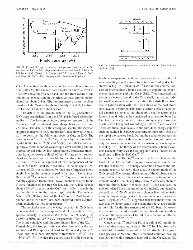
ZnO. Accounting for the energy of the zero-phonon transi-tion �2.86 eV�, the excited state should then have a level at�0.4 eV above the valence band, and the Bohr radius of thehole in the excited state in the effective-mass approximationshould be about 2.4 Å. The luminescence process involvestransfer of the Zn–O orbitals to a highly shielded, localizedlevel in the 3d shell of the Cu atom.
The details of the ground state of the CuZn acceptor inZnO were established from the EPR and infrared-absorptionstudies.372 The low-temperature absorption spectrum of theCu-doped ZnO contained two sharp lines at 717 and722 meV. The details of the absorption spectra, the Zeemansplitting in magnetic field, and the EPR data allowed Dietz etal.372 to construct the following model of CuZn in ZnO. Thefree-ion term 2D of the Cu2+ ion is split by the tetrahedralcrystal field into the 2E�D� and 2T2�D� states that in turn aresplit by a combination of weaker spin-orbit coupling and thetrigonal crystal field. At low temperatures, intracenter transi-tions from the lowest sublevel of the 2T2 state to two sublev-els of the 2E state are responsible for the absorption lines at717 and 722 meV. Assignment of two components of theline at 717 meV �split by �0.1 meV� as being due to twoisotopes of Cu was confirmed by their transformation into asingle line in the crystals doped with only 63Cu isotope.Dietz et al.372 concluded that the Cu2+ t2 wave function isradially expanded �more than e wave function� relative to thed wave function of the free Cu ion, and the t2 hole spendsabout 60% of its time on the Cu2+ ion, while it spends therest of the time in the oxygen sp3 orbitals. The inverse2E�D�→ 2T2�D� transition of the Cu2+ ions in ZnO �a zero-phonon line at 717 meV� has been observed under electron-beam excitation at low temperatures.374
The excited states of the CuZn acceptor in ZnO havebeen revealed in the absorption and PL excitation �PLE�spectra, namely, a characteristic triplet, �, �, and , at2.8594, 2.8680, and 2.8733 eV, respectively �Fig. 77�.375–378
The � line coincides with the zero-phonon line of the GL.371
Remarkably, the isotope shift was also observed in the ab-sorption and PLE spectra, at least for the � and � lines.377
These lines have been attributed to transitions Cu2+�d9�+h�→ �Cu+�d10� ,h� in which the excited state is split into three
levels, corresponding to three valence bands a, b, and c. Aschematic diagram of various transitions in Cu-doped ZnO isshown in Fig. 78. Dahan et al.376 have introduced the con-cept of intermediately bound excitons to explain the experi-mental data associated with Cu in ZnO. They suggested thatthe tenth electron, bound to the Cu d shell, has a larger orbit�or swollen wave function� than the other d-shell electronsdue to hybridization with the Bloch states of the host atoms�the covalent swelling�. This tenth electron creates the poten-tial capturing a hole, so that the tenth d-shell electron and aloosely bound hole can be considered as an exciton bound toCu. Intermediately bound excitons are typically formed incrystals with hexagonal wurtzite-type lattice379 such as ZnO.There are three close levels in the forbidden energy gap forsuch an exciton in ZnO:Cu according to three split levels ofthe top of the valence band. During the excitation process, allthree excited states of the exciton can be observed, whereasonly the lowest one is observed in emission at low tempera-ture �Fig. 78�. The theory of the intermediately bound exci-tons accounts very well the isotope shift and g factors of the�, �, and lines in ZnO:Cu.376,377
Kuhnert and Helbig380 studied the broad phonon side-band of the GL in ZnO �having maximum at 2.4 eV andFWHM of 0.42 eV�. The energy separation between the sub-sequent peaks is 72 meV, close to a LO-phonon mode of theZnO crystal. The spectral distribution of the GL band can bedescribed in terms of the one-dimensional configuration co-ordinate model. The Huang-Rhys factor S=6.5 was obtainedfrom the fitting. Later, Reynolds et al.381 also analyzed thephonon-related fine structure of the GL in ZnO, but identifiedthe peak at �2.26 eV as the zero-phonon line, while attrib-uting the high-energy peaks to hot luminescence. In anotherwork, Reynolds et al.382 suggested that transitions from thetwo shallow donor states to the same deep level are partiallyresponsible for the fine structure of the GL band. However,this picture is in conflict with the fact that different authorsobserved the same shape of the GL fine structure in differentZnO samples.371,375,378,380
Garces et al.,383 studying PL of a bulk ZnO sample be-fore and after annealing in air at 900 °C for 1 h, observed aremarkable transformation of a broad structureless greenband peaking at 500 nm into a structured emission peakingnear 510 nm with a structure identical to the Cu-related GL.
FIG. 77. PL and PLE spectra near the zero-phonon transition of the GLassociated with Cu in ZnO. �Reprinted with permission from P. J. Dean, D.J. Robbins, S. G. Bishop, J. A. Savage, and P. Porteous, J. Phys. C: Solidstate Phys. 14, 2847 �1981�. Copyright 1981, Institute of Physics.�
FIG. 78. A schematic diagram of the transitions in ZnO:Cu �after Dahan etal. �Ref. 376��.
041301-60 Ozgur et al. J. Appl. Phys. 98, 041301 �2005�
[This article is copyrighted as indicated in the article. Reuse of AIP content is subject to the terms at: http://scitation.aip.org/termsconditions. Downloaded to ] IP:
128.172.48.58 On: Mon, 19 Oct 2015 20:45:44
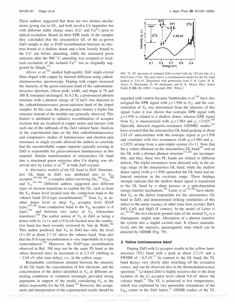
These authors suggested that there are two distinct mecha-nisms giving rise to GL, and both involve Cu impurities butwith different stable charge states �Cu+ and Cu2+� prior tooptical excitation. Based on their EPR study of the samplesthey concluded that the structureless GL of the as-grownZnO sample is due to DAP recombination between an elec-tron bound to a shallow donor and a hole loosely bound tothe Cu+ ion before annealing, while the structured greenemission after the 900 °C annealing was assigned to local-ized excitation of the isolated Cu2+ ion as originally sug-gested by Dingle.371
Alivov et al.384 studied high-quality ZnO single-crystalfilms doped with copper by thermal diffusion using cathod-oluminescence spectroscopy. Doping with copper increasedthe intensity of the green-emission band of the cathodolumi-nescence spectrum, whose peak, width, and shape at 78 and300 K remained unchanged. At 4.2 K, a pronounced phononstructure with a phonon energy of 72 meV was detected inthe cathodoluminescence green-emission band of the dopedsamples. In this case, the phonon peaks feature a triplet finestructure instead of the doublet one generally observed. Thisfeature is attributed to radiative recombination of acceptorexcitons that are localized at copper atoms and interact witheach one of the subbands of the ZnO valence band. Analysisof the experimental data on the film cathodoluminescenceand comparative studies of luminescence and electron-spinresonance in single crystals allowed the authors to concludethat the uncontrollable copper impurity typically existing inZnO is responsible for green-emission luminescence in thismaterial. Similar transformation of structureless GL bandinto a structured green emission after Cu doping was ob-served also by Leiter et al.385 in bulk ZnO crystals.
b. Alternative models of the GL band in ZnO. Structure-less GL band in ZnO was attributed also to VZn
acceptor,359,386–388 a complex defect involving Zni,389 OZn,
390
and VO.391–394 Different authors suggested also differenttypes of electron transitions to explain the GL, such as fromthe VO donor level located near the conduction band to thevalence band �D-h-type recombination�,391 from VO or an-other donor level to deep VZn acceptor level �DAPtype�,387,388 from conduction band to the VZn acceptor �e-Atype�,359 and between two states of VO �intracentertransition�.393 The earlier notion of VO in ZnO as being adonor with its 2+ /+ and +/0 levels located near the conduc-tion band has been recently reviewed by Van de Walle.360
This author predicted that VO in ZnO has only the level�2+ /0� at about 2.7 eV above the valence band. Note alsothat the D-h-type recombination is very improbable in n-typesemiconductor.395 Moreover, the DAP-type recombinationobserved in Ref. 388 may not be the same PL band as theothers detected since its maximum is at 2.3 eV �shifting to�2.04 eV after time delay�, i.e., in the yellow range.
Remarkable correlations attained between the intensityof the GL band, the concentration of free electrons, and theconcentration of the defect identified as VO at different an-nealing conditions or oxidation seemingly provided strongarguments in support of the model considering VO as thedefect responsible for the GL band.391 However, this assign-ment and interpretation of the experimental results should be
regarded with caution because Vanheusden et al.391 have alsoassigned the EPR signal with g=1.956 to VO, and the con-centration of VO was determined from the intensity of thissignal. Later it was shown that isotropic EPR signal withg=1.956 is related to a shallow donor, whereas EPR signalfrom VO is characterized with g� =1.984 and g�=2.025.393
Optically detected magnetic-resonance �ODMR� studies393
have revealed that the structureless GL band peaking at about2.45 eV anticorrelates with the isotropic signal at g=1.956and correlates with two resonances �with g� =1.984 and g�
=2.025� arising from a spin-triplet system �S=1�. Note thatthe g values obtained on the structureless GL band393 and onthe GL with a distinct phonon structure371,383 are incompat-ible, and thus, these two PL bands are related to differentdefects. The triplet resonances were detected only in the en-ergy range of the structureless GL band, while the shallowdonor signal �with g=1.956� quenched the GL band and en-hanced emission in the excitonic range. These findingsstrongly indicate that the shallow donor signal is transferredto the GL band by a shunt process or a spin-dependentenergy-transfer mechanism.393 Leiter et al.393,394 have identi-fied VO as the defect responsible for the structureless GLband in ZnO, and demonstrated striking similarities of thisdefect to the anion vacancy in other ionic host crystals: BaO,SrO, CaO, and MgO �F centers�. In the model of Leiter etal.,393,394 the two-electron ground state of the neutral VO is adiamagnetic singlet state. Absorption of a photon transfersthe system into a singlet excited state. It relaxes nonradia-tively into the emissive, paramagnetic state which can bedetected by ODMR �Fig. 79�.
3. Yellow luminescence band
Doping ZnO with Li acceptor results in the yellow lumi-nescence �YL� band with a peak at about 2.2 eV and aFWHM of �0.5 eV.21 In contrast to the GL band, the YLband decays very slowly after switching off the excitationsource, and can be observed also in the thermoluminescencespectrum.21 Li-doped ZnO is highly resistive due to the deeplocation of the Li acceptor level �about 0.8 eV above thevalence band�.21 The YL is polarized at low temperatures,which was explained by two metastable orientations of theLiZn center in the ZnO lattice.21 ODMR studies of the YL
FIG. 79. PL spectrum of undoped ZnO excited with the 325-nm line of aHeCd laser �5 K�. The inset shows a recombination model for the GL bandpeaked at 2.45 eV. �Reprinted with permission from F. H. Leiter, H. R.Alves, A. Hofstaetter, D. M. Hoffmann, and B. K. Meyer, Phys. StatusSolidi B 226, R4 �2001�. Copyright 2001, Wiley.�
041301-61 Ozgur et al. J. Appl. Phys. 98, 041301 �2005�
[This article is copyrighted as indicated in the article. Reuse of AIP content is subject to the terms at: http://scitation.aip.org/termsconditions. Downloaded to ] IP:
128.172.48.58 On: Mon, 19 Oct 2015 20:45:44

band in ZnO:Li suggest that the DAP-type transitions includ-ing a shallow donor and the Li acceptor dominate at lowtemperatures.396
We observed the YL with metastable behavior also inundoped bulk ZnO. Under irradiation with a He–Cd laser, theGL band gradually bleached, while the YL band emerged andeventually replaced the GL band �Fig. 80�. The YL bandsaturated with excitation intensity above 10−3 W/cm2, indi-cating low concentration of the related defects. The YL wasobserved also in time-resolved PL experiments. The decay ofthe YL is nonexponential at low temperature, allowing thepossibility of the DAP transitions for this band. The YL bandquenched at temperatures above 200 K with the activationenergy of about 0.5 eV.
4. Red luminescence band
A red luminescence �RL� band emerged at about 1.75 eVin the PL spectrum of undoped bulk ZnO after it was an-nealed in air at 700 °C �Fig. 81�. The RL band is broad witha FWHM of about 0.5 eV, and its shape is Gaussian. Withincreasing temperature, the RL band quenches with activa-tion energy of about 15 meV in the range from 15 to 100 K.The quenching of the RL band apparently causes the emer-
gence of the GL band �Fig. 81� This may be a result ofcompetition for holes between the acceptors responsible forthe GL and RL bands. At T�200 K, the GL band quenchesrapidly, so that the RL band is observed alone at room tem-perature �Fig. 81�. Preliminary results of transient PL dem-onstrate that the low-temperature PL decay of the RL band isnearly exponential with a characteristic time of about 1 �s.
VI. DOPING OF ZnO
ZnO has a strong potential for various short-wavelengthoptoelectronic device applications. In order to attain the po-tential offered by ZnO, both high-quality n- and p-type ZnOare indispensable. However, difficulty in bipolar carrier dop-ing �both n and p types� is a major obstacle as seen in otherwide-band-gap semiconductors such as GaN and II-VI com-pound semiconductors including ZnS, ZnSe, andZnTe.397–402 Unipolar doping has not been a surprising issuein wide-band-gap semiconductors: ZnO, GaN, ZnS, andZnSe are easily doped to n-type, while p-type doping is dif-ficult. The situation is opposite for ZnTe where p-type dop-ing is easily obtained, while n-type doping is difficult.
A. n-type doping
ZnO with a wurtzite structure is naturally an n-typesemiconductor because of a deviation from stoichiometrydue to the presence of intrinsic defects such as O vacancies�VO� and Zn interstitials �Zni�. Undoped ZnO shows intrinsicn-type conductivity with very high electron densities ofabout 1021 cm−3.400 Although it is experimentally known thatunintentionally doped ZnO is n type, whether the donors areZni and VO is still controversial. The first-principles studysuggested that none of the native defects show high-concentration shallow donor characteristics.359 However,Look et al.146 suggested that Zni rather than VO is the domi-nant native shallow donor in ZnO with an ionization energyof about 30–50 meV. It has also been suggested that then-type conductivity of unintentionally doped ZnO films isonly due to hydrogen �H�, which, as was treated above �Sec.V�, acts as a shallow donor with an ionization energy about30 meV.359,360,403,404 This assumption is valid since hydrogenis always present in all growth methods and can easily dif-fuse into ZnO in large amounts due to its large mobility.First-principles calculations also suggested that unintention-ally incorporated hydrogen acts as a source of conductivityand behaves as a shallow donor in ZnO.124
n-type doping of ZnO is relatively easy compared top-type doping. Group-III elements Al, Ga, and In as substi-tutional elements for Zn and group-VII elements Cl and I assubstitutional elements for O can be used as n-typedopants.405 Doping with Al, Ga, and In has been attemptedby many groups, resulting in high-quality, highly conductiven-type ZnO films.406–412 Myong et al.406 grew Al-doped ZnOfilms by photoassisted MOCVD method and obtained highlyconductive films with a minimum resistivity of 6.2�10−4 � cm. Ataev et al.407 reported resistivities as low as1.2�10−4 � cm for Ga-doped ZnO films grown bychemical-vapor deposition. Ko et al.411 also succeeded in Gadoping of ZnO films grown on GaN templates by plasma-
FIG. 80. PL spectrum of undoped bulk ZnO annealed at 150 °C in air for1 h. The solid �dashed� curve—after �before� HeCd irradiation for 2 h withan excitation density of 0.3 W/cm2. The excitation density during the mea-surements was 10−3 W/cm2.
FIG. 81. PL spectrum of undoped bulk ZnO at different temperatures. Thesample was annealed at 700 °C in air for 1 h. The excitation density is10−3 W/cm2.
041301-62 Ozgur et al. J. Appl. Phys. 98, 041301 �2005�
[This article is copyrighted as indicated in the article. Reuse of AIP content is subject to the terms at: http://scitation.aip.org/termsconditions. Downloaded to ] IP:
128.172.48.58 On: Mon, 19 Oct 2015 20:45:44

assisted MBE. Thus, n-type doping of ZnO is developed verywell. Such films are successfully used in various applicationsas n-type layers in light-emitting diodes as well as transpar-ent Ohmic contacts as will be discussed below.
B. p-type doping
As mentioned repeatedly it is very difficult to obtainp-type doping in wide-band-gap semiconductors, such asGaN and ZnSe. The difficulties can arise from a variety ofcauses. Dopants may be compensated by low-energy nativedefects, such as Zni or VO,413 or background impurities �H�.Low solubility of the dopant in the host material is alsoanother possibility.414 Deep impurity level can also be asource of doping problem, causing significant resistance tothe formation of shallow acceptor level.
Known acceptors in ZnO include group-I elements suchas lithium �Li�,21,415,416 Na, and K, copper �Cu�,417 silver�Ag�,418 Zn vacancies, and group-V elements such as N, P,and As. However, many of these form deep acceptors and donot contribute significantly to p-type conduction. It has beenbelieved that the most promising dopants for p-type ZnO arethe group-V elements, although theory suggests some diffi-culty in achieving shallow acceptor level.419
A number of theoretical studies have addressed the fun-damental microscopic aspects of doping in wide-band-gapsemiconductors. The majority of these studies have dealtwith the manner in which dopant solubility397,420 or nativedefects421,422 such as vacancies, interstitials, and antisites in-terfere with doping. Recently, various substitutional impuri-ties for ZnO were examined as p-type dopants by using thefirst-principles pseudopotential method.419,423,424
p-type doping in ZnO may be possible by substitutingeither group-I elements �Li, Na, and K� for Zn sites orgroup-V elements �N, P, and As� for O sites. It was shownthat group-I elements could be better p-type dopants thangroup-V elements in terms of shallowness of acceptor levelsas shown in Table XVII.419 However, group-I elements tendto occupy the interstitial sites, in part mitigated by their smallatomic radii, rather than substitutional sites, and therefore,act mainly as donors instead.425 Moreover, significantlylarger bond length for Na and K �see Table XVII� than idealZn–O bond length �1.93 Å� induces lattice strain, increas-ingly forming native defects such as vacancies which com-pensate the very dopants. These are among the many causesleading to difficulties in attaining p-type doping in ZnO. A
similar behavior is observed for group-V elements except forN. Both P and As also have significantly larger bond lengthsand, therefore, are more likely to form antisites to avoid thelattice strain. The antisites, AZn, are donorlike and provideyet another unwelcome possible mechanism for compensat-ing acceptors. It then appears that perhaps the best candidatefor p-type doping in ZnO is N because among the group-Vimpurities, N has the smallest ionization energy, it does notform the NZn antisite, and the AX center of N is onlymetastable.419
Kobayashi et al.426 also predicted that N is a good can-didate for a shallow p-type dopant in ZnO although N is notvery soluble in ZnO, suggesting that N doping can be achiev-able by ion implantation. Somewhat related to the currenttopic, Wu et al.427 have demonstrated shallow N acceptors inN+-implanted ZnSe using PL measurements. It is now wellknown that reactive N produced p-type ZnSe which led todemonstration of laser diodes before supplanted by GaN-based diode lasers.428 However, p-type doping of ZnO hasnot been successful using pure nitrogen source,429 while ac-ceptor concentrations as high as 1018 cm−3 have been ob-tained for ZnSe using an N2 plasma source.430 This impliesthat N acceptors are more readily compensated in ZnO ascompared to ZnSe.
1. Nitrogen doping
Helped by success with ZnSe nitrogen has been exploredfor p-type doping of II-VI semiconductors.430–432 A numberof groups have expended a good deal of effort in an attemptto realize p-type ZnO using nitrogen �N� as a possible shal-low acceptor dopant. Various types of nitrogen sources in-cluding N2, NO, N2O, NH3, and Zn3N2 have been used de-pending on the growth technique, as elaborated on below.
Iwata et al.433 have attempted p-type doping of ZnO us-ing MBE by simultaneously introducing O2 and N2 through arf plasma source. Although a nitrogen concentration as highas 1019 cm−3 was obtained, conduction-type conversion fromn-type to p-type did not occur. However, some promisingresults were reported recently. Look et al.365 reported p-typeZnO by MBE with N doping �performed by Eagle Picher�using Li-diffused semi-insulating ZnO substrates and an N2
rf plasma source. Nitrogen-surface concentration �1019 cm−3�in the N-doped ZnO film measured by secondary-ion-massspectroscopy �SIMS� was two orders of magnitude higherthan that in undoped ZnO, implying the presence of highdoping. The N-doped ZnO showed p-type behavior with ahole concentration of 9�1016 cm−3 and a hole mobility of2 cm2/V s. The PL spectrum of Fig. 82 shows a strong peaknear 3.32 eV probably due to neutral-acceptor-bound exci-tons. The estimated acceptor level was between 170 and200 meV based on the low-temperature PL measurements.
Ashrafi et al.434 also used nitrogen as a p-type dopant inconjunction with H2O vapor as an oxygen source in metal-organic MBE. Thermal annealing increased the net acceptorconcentration �NA–ND� by approximately two orders ofmagnitude ��5�1016 cm−3�. Ashrafi et al. observed p-typeconductivity in spite of higher H concentration than that ofN, suggesting that H may be more closely correlated to
TABLE XVII. Calculated nearest-neighbor bond lengths, the defect energylevels �Ei� for negatively charged substitutional impurities, and the energy��E� required to form the positively charged AX center from the substitu-tional acceptors �Park et al. �Ref. 419��.
Element Bond length �� Ei �eV� �E
Li 2.03 0.09 0.21Group I Na 2.10 0.17 1.04
K 2.42 0.32 1.38N 1.88 0.40 0.13
Group V P 2.18 0.93 −0.46As 2.23 1.15 −0.18
041301-63 Ozgur et al. J. Appl. Phys. 98, 041301 �2005�
[This article is copyrighted as indicated in the article. Reuse of AIP content is subject to the terms at: http://scitation.aip.org/termsconditions. Downloaded to ] IP:
128.172.48.58 On: Mon, 19 Oct 2015 20:45:44

p-type conductivity rather than being simply a shallow donoror causing passivation, as the theory suggests.
Several groups obtained p-type ZnO films by addingNH3 in O2 or H2 gas as a nitrogen source. Minegishi et al.435
reported the growth of p-type ZnO using chemical-vapordeposition �CVD�. The NH3 gas was simultaneously addedin the hydrogen carrier gas with excess Zn. The resistivity ofthe resulting films was high �100 � cm�, suggesting that theacceptor level is relatively deep with a subsequent low free-hole concentration. Ye et al.436 also used NH3 as the nitrogensource for dc reactive magnetron sputtering of p-type ZnO.Results show a hole concentration of 3.2�1017 cm−3 and aresistivity of 35 � cm. Ye et al. proposed that the excess zincand interstitial hydrogen play an important role in p-typedoping as suggested by Ashrafi et al.434 However, the role ofhydrogen in N-doped ZnO was explained somewhat differ-ently by Wang et al.437 They argued that when NH3 increasesin the MOCVD chamber, more hydrogen atoms are absorbedonto the substrate surface and introduced in the film due tothe O–H bond which is stronger than the Zn–N bond, result-ing in a decrease in the nitrogen concentration.
Lu et al.438 investigated p-type ZnO growth as a functionof ammonia concentration in NH3–O2 ambient using dc re-active magnetron sputtering. While N-doped p-type ZnOfilms were achieved at ammonia concentration of 25%–75%,intrinsic ZnO film and zinc polycrystal film were obtained at0% and 100% ammonia concentrations, respectively. It can-not be understated that despite reports of p-type conductivity,the issue is still controversial. Much of the problem arisesfrom very low mobilities in Hall experiments and a gooddeal of carrier localization in these ZnO films doped withimpurities thought to lead to p-type doping. The reference top-type conductivity here merely reflects what has been re-ported, and nothing more. At 50% ammonia concentration,better electrical properties were obtained: hole concentrationof 7.3�1017 cm−3, hole mobility of 1.3 cm2/V s, and resis-tivity of 31 � cm. The results showed that the nitrogen in-corporation in ZnO is increased in the presence of NH3, en-hancing the hole concentration. However, when ammoniaconcentration is high �100%�, the densities of VO and Zni areincreased due to absence of O2 in ambient, resulting in zincpolycrystalline film.
One chain of thought is that to attain p-type ZnOthrough N doping it may be necessary to provide oxygenalso to suppress oxygen vacancy VO. One approach could beto use an O2/N2 mixture. However, at least in one instance,such an effort did not turn out successful and p-type conduc-tivity was not obtained, even though various ratios of O2/N2
were employed.439
As a nitrogen source some researchers used N2O gas,which is a mild oxidizing gas �stronger than O2 and weakerthan NO2 as an oxidizing agent�. Very pertinent to the topicof discussion is that the dissociation energy �N–N:5.16 eVand N–O:6.37 eV� and ionization potential �N2O:12.9 eV�of N2O are lower than those of N2 �N–N:9.76 eV andN2:15.65 eV�.440 In this vein, Guo et al.440 used N2O plasmafor nitrogen doping of ZnO film by PLD. They found thatnitrogen doping was enhanced using the active N formed byN2O gas flowing through an electron-cyclotron-resonance�ECR� source. The samples showed p-type conductivity witha hole concentration in the range of 3�1018–6�1018 cm−3,resistivity in the range of 2–5 � cm, and hole mobility inthe range of 0.1–0.4 cm2/V s.
Based on first principles Yan et al.441 proposed that thenitric oxide �NO� gas without an ECR plasma source is moreefficient as a N source than N2O or N2. The model indicatedthat the defect formation energy of N on oxygen site, NO,from NO should be lower than that from N2O. As shown inFig. 83 the formation energy of NO is negative under Zn-richconditions, implying that no additional energy is required forNO formation, while the formation energy of NO from N2 ispositive, suggesting that additional energy is needed �e.g.,plasma or high temperature�. Even though the formation en-ergy of NO from N2O is negative, the energy is much largerthan that from NO. Therefore, it was suggested that NO mol-ecules can be incorporated spontaneously to form NO defectsin ZnO.
FIG. 82. PL spectra, at 2 K, for two ZnO samples, an undoped bulk sampleand a N-doped, MBE-grown epitaxial layer. �Reprinted with permissionfrom D. C. Look, D. C. Reynolds, C. W. Litton, R. L. Jones, D. B. Eason,and G. Cantwell, Appl. Phys. Lett. 81, 1830 �2002�. Copyright 2002, Ameri-can Institute of Physics.�
FIG. 83. �a� Calculated formation energies of NO as functions of the Ochemical potential formed by atomic N �stripped off a N2 or a N2O mol-ecule�, NO, or NO2 molecule. �O=−3.3 is the Zn-rich limit condition and�O=0 is the O-rich limit condition. �b� Calculated formation energies of a�N2�O as functions of the O chemical potential for the defects formed by N2,N2O, NO, and NO2 molecules. �Reprinted with permission from Y. Yan, S.B. Zhang, and S. T. Pantelides, Phys. Rev. Lett. 86, 5723 �2001�. Copyright2001 by the American Physical Society.�
041301-64 Ozgur et al. J. Appl. Phys. 98, 041301 �2005�
[This article is copyrighted as indicated in the article. Reuse of AIP content is subject to the terms at: http://scitation.aip.org/termsconditions. Downloaded to ] IP:
128.172.48.58 On: Mon, 19 Oct 2015 20:45:44

Wang et al.442 attempted nitrogen doping in ZnO filmsby plasma-assisted MOCVD using diethyl zinc �DEZn� andN2 gas, but p-type behavior was not obtained. However, Li etal.443,444 claimed to have succeeded in p-type doping of ZnOfilms, by reacting DEZn with NO gas. In this case, NO gaswas used to supply both O and N for p-type doping. Resultsindicated that N can be incorporated into ZnO films withoutplasma or high-temperature process and a high N concentra-tion was obtained only under Zn-rich conditions as predictedby Yan et al.441 It should be stated that N does indeed incor-porate as an acceptor. However, a sufficient amount of ac-ceptors should be generated to overcome the n-type back-ground or any other donorlike defects introduced throughparasitic processes.
As discussed earlier, the solubility of nitrogen in ZnO islow and N from NO is more efficiently incorporated intoZnO than that from N2. However, a different approach forgrowing N-doped p-type ZnO films was reported in Ref.445. p-type ZnO was obtained after thermal annealing ofzinc oxynitride �ZnON� alloy films deposited by rf reactivemagnetron sputtering. The samples were grown at a rela-tively low substrate temperature of 200 °C compared toothers436,438 and were subjected to postgrowth thermal an-nealing, resulting in the transformation from ZnON alloy toZnO. In this case, annealing at a temperature of 600 °C ledto p-type behavior of the films. Further increase of the an-nealing temperature to 1000 °C in oxygen ambient elimi-nated all the N dopants and replaced them by O even thoughthe crystalline quality was improved. Results indicated thatthere is a tradeoff between N-doping efficiency and crystal-line quality.
Lin et al.446 obtained what has been referred to as p-typeZnO by nitrogen-ion implantation of ZnO films grown on Sisubstrates with SiN buffer layers using rf magnetron sputter-ing. The p-type ZnO films implanted with 5�1012–1�1014 cm−2 N+ dose showed good electrical properties �holeconcentration of 5.0�1016–7.3�1017 cm−3, hole mobilityof 2.51–6.02 cm2/V s, and resistivity of 10.1–15.3 � cm�.
While most studies on N-doped p-type ZnO have beenbased on deposition methods, other approaches such as oxi-dation have been attempted as well. N-doped ZnO was ob-tained by oxidizing Zn3N2 films, which were deposited by dcmagnetron sputtering.447 A sample oxidized at 500 °Cshowed p-type characteristics with a hole concentration of5.8�1018 cm−3. However, oxidization at a higher tempera-ture of 550 °C resulted in n-type conductivity which wasstated to be due to insufficient N atoms to form N acceptors.
Enhancement of N doping in ZnO by thermal treatmenthas been undertaken. Garces et al.448,449 observed the forma-tion of nitrogen acceptors in N-doped ZnO crystals usingphotoinduced electron-paramagnetic-resonance �EPR�method after annealing in air or nitrogen atmosphere at atemperature range of 600–900 °C. The pathway for this wasreported to be due to nitrogen substitution for the shallowimpurity donors during the thermal treatment.
Solid-source chemical-vapor deposition450 �SS-CVD�was also used for nitrogen doping of ZnO. Zinc acetate di-hydrate �Zn�CH3COO�2 ·2H2O, solid� and ammonium ac-etate �CH3COONH4, solid� were used as the precursor and
the nitrogen source, respectively. The samples showed p-typeconductivity with a hole concentration of 9.8�1017 cm−3,resistivity of 20 � cm, and hole mobility of 0.97 cm2/V s.
Despite the above-mentioned reports on successfulgrowth of p-type ZnO films by N doping, there were also anumber of reports in which the authors were not able toreproduce these results even when the same growth methods,growth conditions, and N precursors were used.440,451–453
Therefore, even if one assumes that the reported results rep-resent truly p-type ZnO, the reproducibility still remains tobe a major problem, and this must be solved before ZnO canbe used in optoelectronics applications such as homojunctionLEDs and laser diodes �LDs�. Finally, until ZnO p-n junc-tions with at least good injection efficiencies are attained,questions will be raised.
2. Codoping method: Nitrogen+group III
Although nitrogen has been considered as the best can-didate for p-type doping for ZnO, it is well known that thesolubility of N in ZnO is low. Therefore, it is necessary tofind methods which can enhance the solubility limit of N inZnO. For this purpose, a donor-acceptor codoping methodhas been proposed in order to realize highly conductingp-type ZnO,454,455 and the experimental studies based on thisapproach have been performed.456–462
Recently, Yamamoto and Katayama-Yoshida454 proposedthe codoping method to solve the unipolarity in ZnO basedon ab initio electronic band-structure calculations. The en-hancement in solubility to a level well above the solubilitylimit was explained in terms of the formation of ion pairsbetween donor and acceptor ions and a consequent reductionin the Madelung energy. While the Madelung energy de-creases with group-III elements �Al, Ga, and In� for n-typedoping, it increases with group-V element N for p-type dop-ing, indicating localization of the N states.
Figure 84 shows the crystal structure of supercells forZnO:�Ga, 2N� and the formation of complexes, III-N pairs,which occupy the nearest-neighbor sites and the next-nearest-neighbor sites based on ab initio total-energy calcu-lations. It is also indicated that there were no stable configu-
FIG. 84. Crystal structure of a supercell for ZnO:�Ga, 2N�. �Reprinted fromT. Yamamoto, Thin Solid Films 420–421, 100 �2002�, Copyright 2002, withpermission from Elsevier.�
041301-65 Ozgur et al. J. Appl. Phys. 98, 041301 �2005�
[This article is copyrighted as indicated in the article. Reuse of AIP content is subject to the terms at: http://scitation.aip.org/termsconditions. Downloaded to ] IP:
128.172.48.58 On: Mon, 19 Oct 2015 20:45:44

rations for ZnO:2N with the same N concentration, holdingout the possibility that N incorporation can be enhanced withthe group-III elements.
It is reported that codoping of N with the reactant dop-ants lowers the acceptor level in the band gap due to stronginteraction between N acceptors and reactive donorcodopants. As shown in Figs. 85�b�–85�d� the shift of theDOS peak toward the top of the valence band implies thatthe acceptor levels are lowered. Yamamoto andKatayama-Yoshida454 also proposed the codoping with Li asan acceptor with F as reactive donor codopants for thegrowth of low-resistivity p-type ZnO.
A SIMS study on the solubility limits of Ga and N inZnO showed the enhancement of N solubility limit in coim-planted ZnO by a factor of 400 as compared to that inN-implanted ZnO. Using the codoping method, Joseph etal.463 successfully grew what was termed as p-type ZnOfilms by a PLD system combined with a plasma gas source.For Ga and N codoping, N2O gas was used as the nitrogensource instead of N2 gas, since N2O gas is effective in sup-pressing oxygen vacancies, and introduce N as an acceptorsimultaneously. p-type conductivity was confirmed usingHall and Seebeck coefficient measurements with a resistivityof 0.5 � cm, a carrier concentration of 5�1019 cm−3, and avery low mobility of 0.07 cm2/V s. The very low mobilitybrings the p-type conductivity in question. It was also indi-
cated that low-temperature formation is essential for non-equilibrium growth in the codoping technique. Althoughp-type conductivity was observed in codoped ZnO films, theorigin of p-type characteristics is not clear due to the lack ofcharacterization, such as the donor and acceptor levels in theband gap for the Ga and N dopants.
Ohshima et al.459 have attempted to synthesize p-typeZnO by PLD using various codoping methods including theablation of ZnO:Ga target in NO gas, and Al and N codopingusing an ion gun and a microwave ECR source. Althoughthey could identify the presence of Ga–N bond in ZnO,p-type ZnO film could not be obtained.
It was reported that the types of conductivity and carrierconcentration in Ga and N codoped ZnO are dependent onthe O2 partial pressure in the sputtering gas mixture. Singh etal.464 observed n-type conduction for deposited films foroxygen partial pressures between 0% and 40%. The conduc-tion type of films deposited in the 40%–50% oxygen partialpressure range was not clearly identifiable due to large resis-tivity. But the films deposited with partial pressures higherthan 50% showed p-type conduction. Assuming that thep-type conductivity is real, this dependence of the conduc-tion type on oxygen partial pressure showed the importantrole of oxygen vacancies in the type of conductivityachieved. Thus, as the O2 partial pressure increases, VO andZni are suppressed or the background donor concentration isinsufficient to compensate the acceptors from N substitutionin ZnO, paving the way for p-type conduction �see Fig.86�a��. When the O2 partial pressure ratio was increasedfrom 50% to 60%, the mobility and resistivity decreasedwhile the hole concentration increased, as shown in Fig.
FIG. 85. Site-decomposed DOS of p states at the N sites for �a� ZnO:N, �b�ZnO:�Al, 2N�, �c� ZnO:�Ga, 2N�, and �d� ZnO:�In, 2N�. The dotted curveindicates the DOS at the N atom sites close to the reactive donor codopant;the solid curve indicates the DOS at the sites of next-nearest-neighbor Natoms. �Reprinted from T. Yamamoto and H. Katayama-Yoshida, J. Cryst.Growth 214/215, 552 �2000�, Copyright 2000, with permission fromElsevier.�
FIG. 86. �a� Effect of oxygen partial pressure ratio on conduction type ofcodoped ZnO films. �b� Hole concentration, resistivity, and Hall mobility asa function of oxygen partial pressure. �Reprinted with permission from A. V.Singh, R. M. Mehra, A. Wakahara, and A. Yoshida, J. Appl. Phys. 93, 396�2003�. Copyright 2003, American Institute of Physics.�
041301-66 Ozgur et al. J. Appl. Phys. 98, 041301 �2005�
[This article is copyrighted as indicated in the article. Reuse of AIP content is subject to the terms at: http://scitation.aip.org/termsconditions. Downloaded to ] IP:
128.172.48.58 On: Mon, 19 Oct 2015 20:45:44

86�b�. However, further increase in the O2 partial pressureratio caused a decrease in the mobility and an increase in theresistivity, probably because of the degradation of crystalquality due to oxygen-induced defects.
There were also reports on codoping experiments inwhich indium465 �In� and aluminum466 �Al� were used asgroup-III codoping metals. In codoping studies with In ultra-sonic ultraspray pyrolysis method was used for growth. Theaqueous solutions Zn�CH3 OO�2 ·H2O �AR, 0.5 mol/ l�,�CH3 OONH4�2 �AR, 2.5 mol/ l�, and In�NO�3 �AR,0.5 mol/ l� were used as the sources of the Zn, N, and In,respectively. The grown p-type ZnO films had low film re-sistivity �1.7�10−2 � cm�, high hole concentration �2.44�1018 cm−3�, and incredibly high hole mobility�155 cm2/V s� which brings the validly of these results intoquestion. Al+N codoping was performed during growth ofZnO films in a N2O+O2 atmosphere on glass substrates bydc reactive magnetron sputtering. At a substrate temperatureof 500 °C, p-ZnO was realized with hole densities as largeas 1.1�1017 cm−3.
In other codoping experiments, however,457,458,461 nop-type conductivity was observed even though a N concen-tration as high as 2�1020 cm−3 was obtained in ZnO. How-ever, such codoped ZnO layers in these experiments exhib-ited a dramatic increase �by eight to nine orders ofmagnitude� in resistivity. The formation of N–Ga–N acceptorcenters in the samples was suggested to be the reason.
3. Other dopants in group V
While most efforts on p-type doping of ZnO have fo-cused on nitrogen doping with/without codopants because ofits relatively shallow level, considerably fewer studies haveconsidered other group-V elements for substitutional dopingon the O sites370,467–472 Only in some of these studies inver-sion of the film’s conductivity type was observed.
Aoki et al.467 used the PLD technique to producephosphorus-doped p-type ZnO films using a zinc-phosphide�Zn3P2� compound as the phosphorus source. In this process,a Zn3P2 film deposited on a ZnO substrate was exposed toexcimer laser radiation in high-pressure nitrogen or oxygenambient and was consequently decomposed into Zn and Patoms which diffuse into ZnO, resulting in the formation ofP-doped ZnO through the replacement of O atoms by P at-oms. In this case, a p-n-junction-like behavior was observedbetween an n-type ZnO substrate and a surface P-doped layeralthough Hall measurements did not confirm p-type conduc-tivity. Similar results were obtained by Lee et al.473 who alsotransformed a Zn3P2 layer on ZnO/sapphire to p-type ZnOby laser annealing.
Recently, Kim et al.468 reported that a phosphorus-dopedn-type ZnO film grown by rf sputtering using P2O5 as thephosphorus source led to p-type ZnO by thermal annealing ata temperature above 800 °C in N2 ambient �Fig. 87�. Duringthe thermal activation of dopants, P2O5 dissociates and con-sequently the phosphorus atoms act as acceptors and oxygenatoms may compensate oxygen vacancies which otherwisewould act as compensating donors. The ZnO films showedp-type behavior with a hole concentration of 1.0�1017–1.7�1019 cm−3, a mobility of 0.53–3.51 cm2/V s,
and a low resistivity of 0.59–4.4 � cm. The PL spectrumshowed a strong peak at 3.35 eV, which is probably due toneutral-acceptor-bound excitons as observed by Look etal.425 Afterwards such p-type ZnO films were grown onn-type GaN to fabricate p-ZnO-/n-GaN-typeheterostructures.474 Quite good p-n heterojunctions and elec-troluminescense properties were observed.
Another group was unsuccessful in achieving p-typeZnO using phosphorus;472 however, they recently demon-strated p-type behavior in P-doped ZnMgO layers grown bypulsed-laser deposition.475 The different behavior of phos-phorus in ZnO and ZnMgO layers is still not clear.Phosphorus-doped Zn0.9Mg0.1O targets were fabricated usinghigh-purity ZnO �99.9995%� and MgO �99.998%�, withP2O5 �99.998%� serving as the doping agent. The majority-carrier-type was determined from capacitance-voltage char-acteristics of metal-insulator-semiconductor devices fabri-cated, and the hole concentration and mobility wereestimated to be 2�1018/cm3 and 0.01–0.001 cm2/V s, re-spectively. Minority-carrier transport properties ofp-Zn0.9Mg0.1O were studied by employing electron-beam-induced current and cathodoluminescence methods,476
and the electron diffusion length and lifetime were foundto be �2.12 �m and �34 ns, respectively. Both of thesevalues increased after electron-beam irradiation. Using thesep-type layers Zn0.9Mg0.1O/ZnO p-n junctions were fabri-cated with good rectifying diodelike current-voltagecharacteristics.475,477
Ryu et al.469 employed GaAs substrates as an arsenicsource for p-type doping of ZnO by PLD. In this case, ap-type ZnO layer was produced at the ZnO/GaAs interfaceafter thermal annealing. Recently, p-type ZnO films weregrown on different substrates, ZnO, SiC, and sapphire, rather
FIG. 87. Carrier concentration of phosphorus-doped ZnO thin films treatedby RTA �Reprinted with permission from K.-K. Kim, H.-S. Kim, D.-K.Hwang, J.-H. Lim, and S.-J. Park, Appl. Phys. Lett. 83, 63 �2003�. Copy-right 2003, American Institute of Physics.�
041301-67 Ozgur et al. J. Appl. Phys. 98, 041301 �2005�
[This article is copyrighted as indicated in the article. Reuse of AIP content is subject to the terms at: http://scitation.aip.org/termsconditions. Downloaded to ] IP:
128.172.48.58 On: Mon, 19 Oct 2015 20:45:44
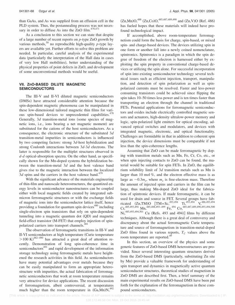
than GaAs, and As was supplied from an effusion cell in thePLD system. Thus, the postannealing process was not neces-sary in order to diffuse As into the ZnO film.470,471
As a conclusion to this section we can state that despiteof a large number of recent reports on p-type ZnO growth byvarious methods,50 no reproducible high-quality p-type lay-ers are available yet. Further efforts to solve this problem areneeded. In particular, careful analysis of the experimentaldata �particularly the interpretation of the Hall data in casesof very low Hall mobilities�, better understanding of thephysical properties of point defects in ZnO, and developmentof some unconventional methods would be useful.
VII. ZnO-BASED DILUTE MAGNETICSEMICONDUCTORS
The III-V and II-VI diluted magnetic semiconductors�DMSs� have attracted considerable attention because thespin-dependent magnetic phenomena can be manipulated inthese low-dimensional tailored magnetic thin films for vari-ous spin-based devices to unprecedented capabilities.478
Generally, 3d transition-metal ions �some species of mag-netic ions, i.e., ions bearing a net magnetic moment� aresubstituted for the cations of the host semiconductors. As aconsequence, the electronic structure of the substituted 3dtransition-metal impurities in semiconductors is influencedby two competing factors: strong 3d-host hybridization andstrong Coulomb interactions between 3d-3d electrons. Thelatter is responsible for the multiplet structures observed ind-d optical-absorption spectra. On the other hand, as specifi-cally shown for the Mn-doped systems the hybridization be-tween the transition-metal 3d and the host valence bandgives rise to the magnetic interaction between the localized3d spins and the carriers in the host valence band.479
With the significant advance of the materials engineeringof thin-film and nanoscale heterostructures, the quantized en-ergy levels in semiconductor nanostructures can be coupledeither with local magnetic fields created by integrated sub-micron ferromagnetic structures or with the exchange fieldsof magnetic ions into the semiconductor lattice itself, henceproviding a foundation for quantum spin devices480 includingsingle-electron spin transistors that rely on spin-dependenttunneling into a magnetic quantum dot �QD� and magneticfield-effect transistor �M-FET� that employ injection of spin-polarized carriers into transport channels.481
The observation of ferromagnetic transitions in III-V andII-VI semiconductors at high temperature �Curie temperature�100 K�482–490 has attracted a great deal of attention re-cently. Demonstration of long spin-coherence time insemiconductors491 and rapid development of the informationstorage technology using ferromagnetic metals have height-ened the research activities in this field. As semiconductorshave many potential advantages over metals because theycan be easily manipulated to form an appropriate hetero-structure with impurities, the actual fabrication of ferromag-netic semiconductors that work at room temperature remainsvery attractive for device applications. The recent discussionof ferromagnetism, albeit controversial, at temperaturesmuch higher than the room temperature in �Ga,Mn�N,492
�Zn,Mn�O,488 �Zn,Co�O,485,487,489,490 and �Zn,V�O �Ref. 486�has fueled hopes that these materials will indeed have pro-found technological impact.
If accomplished, above room-temperature ferromag-netism could form the basis for charge, spin-based, or mixedspin- and charge-based devices. The devices utilizing spin inone form or another fall into a newly coined nomenclature,spintronics. Spintronics is a paradigm in which the spin de-gree of freedom of the electron is harnessed either by ex-ploiting the spin property in conventional charge-based de-vices or utilizing the spin alone. For successful incorporationof spin into existing semiconductor technology several tech-nical issues such as efficient injection, transport, manipula-tion, and detection of spin polarization as well as spin-polarized currents must be resolved. Faster and less-powerconsuming transistors could be achieved since flipping thespin takes 10–50 times less power and is ten times faster thantransporting an electron through the channel in traditionalFETs. Potential applications for ferromagnetic semiconduc-tors and oxides include electrically controlled magnetic sen-sors and actuators, high-density ultralow-power memory andlogic, spin-polarized light emitters for optical encoding, ad-vanced optical switches and modulators, and devices withintegrated magnetic, electronic, and optical functionality.Challenges are formidable in that in addition to coherent spininjection, the device dimensions must be comparable if notless than the spin-coherence lengths.
Assuming that ZnO can be made ferromagnetic by dop-ing with transition metals such as Mn, Fe, Cr, Co, etc., orwhen spin injecting contacts to ZnO can be found, the ma-terial would be suitable for spin FETs. In ZnO, the equilib-rium solubility limit of 3d transition metals such as Mn islarger than 10 mol %, and the electron effective mass is aslarge as �0.3me, where me is free-electron mass. Thereforethe amount of injected spins and carriers in the film can belarge, thus making Mn-doped ZnO ideal for the fabrica-tion of spintronic devices. If made ferromagnetic, it can beused for drain and source in FET. Several groups have fab-ricated �Zn,TM�O �TM=Sc,493,494 Ti,493,494 V,486,493,494
Cr,485,493,494 Mn,485,488,493–499 Fe,494 Co,485,487,489,490,493,494,500
Ni,485,493,494,501 Cu �Refs. 493 and 494�� films by differenttechniques. Although there is a great deal of controversy anddiscrepancy about the actual ferromagnetic Curie tempera-ture and source of ferromagnetism in transition-metal-dopedZnO films found in various reports, TC values above theroom temperature are reported.49
In this section, an overview of the physics and somegeneric features of ZnO-based DMS heterostructures are pro-vided. Since several interesting quantum structures derivedfrom the ZnO-based DMS �particularly, substituting Zn siteby Mn� provide a valuable framework for understanding ofspin transport and dynamics in magnetically active quantumsemiconductor structures, theoretical studies of magnetism inZnO DMS are described first. Then, a brief summary of themain experimental results on ZnO-based DMS have been putforth for the explanation of the ferromagnetism in these com-pound semiconductors.
041301-68 Ozgur et al. J. Appl. Phys. 98, 041301 �2005�
[This article is copyrighted as indicated in the article. Reuse of AIP content is subject to the terms at: http://scitation.aip.org/termsconditions. Downloaded to ] IP:
128.172.48.58 On: Mon, 19 Oct 2015 20:45:44
A. Theory of ZnO-based magnetic semiconductors
There are two basic approaches in understanding themagnetic properties of dilute magnetic semiconductors. Thefirst group of approaches, which are based on the generalmean-field theory, implicitly assumes that the dilute mag-netic semiconductor is a more-or-less random alloy, e.g., �Zn,TM�O, in which transition-metal �TM� substitutes for one ofthe lattice constituents. The ferromagnetism occurs throughinteractions between the local moments of the TM atoms,which are mediated by free carriers in the material. The spin-spin coupling is also assumed to be a long-range interaction,allowing use of a mean-field approximation. Virtual crystalapproximation is used to calculate the effective spin densitydue to the TM-ion distribution. The direct TM-TM interac-tions are antiferromagnetic so that the Curie temperature TC
for a given material with a specific TM concentration andhole density is determined by a competition between the fer-romagnetic and antiferromagnetic interactions. The secondgroup of approaches suggests that the magnetic atoms formclusters that produce the observed ferromagnetism. It is ex-perimentally difficult to verify the mechanism responsiblefor the observed magnetic properties, because depending onthe growth conditions employed for growing the DMS ma-terial, it is likely that one could readily produce samplesconsisting of single-phase random alloys, nanoclusters of themagnetic atoms, precipitates and second-phase formation, ora combination of these. To decide which mechanism is ap-plicable, one should carefully correlate the measured mag-netic and magnetoelectric properties with material analysismethods that are capable of detecting other phases or precipi-tates. If, for example, the magnetic behavior of the DMS is acharacteristic of a known ferromagnetic second phase, thenclearly the mean-field models are not applicable.
Principally, the majority of DMS studied in an extensiveway until now involved Mn2+ ion as a legitimate member ofthe transition-metal family to be embedded in various II-VIand III-V hosts. The easy substitution of Mn for the group-IIelements in both zinc-blende and wurtzite structures occursmainly due to the fact that the 3d orbitals of Mn2+ are exactlyhalf-filled. As a consequence, all five spins are parallel in thisorbital by Hund’s rule and that will cost a considerable en-ergy to add an electron with opposite spin to the atom, re-sulting in a complete 3d5 orbit. Therefore, Mn2+ has a rela-tively large magnetic moment �spin S=5/2 and angularmomentum L=0� with characteristic of a half-filled d shelland can be incorporated in sizable amounts �up to 35% ofMn� into ZnO host without affecting much the crystallo-graphic quality of the DMS, whereas about 5% is tolerablefor III-V-based hosts. Additionally, Mn2+ is electrically neu-tral in II-VI hosts acting as neither acceptor nor donor, whileit acts as an acceptor in the III-V-based DMS. In view of this,Mn atom resembles a group-II element, hence has attractedmany researchers to produce these materials using both thin-film and bulk growth techniques. With the advancement ofenhanced MBE growth techniques, heterostructures contain-ing a variety of band alignments, strain configurations, andDMS alloys can and have been fabricated. One may employthe band-gap engineering techniques to create new DMS ma-
terials by manipulating the various physical parameters in-volved. Apart from this, the presence of local moments al-lows the spin engineering of phenomena through theexploitation of two classes of exchange interactions. The firstone is the d-d superexchange between d electrons of themagnetic ions, and the second one is the sp-d exchange be-tween the d electrons and the band electrons or holes. Thisinteraction is ferromagnetic for conduction-band states andmainly antiferromagnetic for valence bands. This interactiondetermines the spin splitting of the band states in an externalmagnetic field, giving rise to interesting magneto-optical andmagnetotransport responses in the DMS samples.
To obtain the Curie temperature from the magnetic mea-surements, the Curie-Weiss law is used:
M
H=
C0x
T − �0x, �28�
where M is the magnetization, H is the magnetic field, T isthe temperature, x is the transition-metal composition, and�0 and C0 are the Curie-Weiss temperature and the Curieconstant for x=1, respectively. The Curie constant may beexpressed as496
C0 =�g�B�2S�S + 1�n
3kB= CM
�
�, �29�
where g is the intrinsic Lande g factor, n is the number ofcation sites per unit volume, CM is the Curie constant for x=1, � is the mass density, � is the molar mass, S is theeffective spin per transition-metal ion �S=3/2 for Mn2+�, �B
is the Bohr magneton, and kB is the Boltzman constant. Us-ing Eqs. �28� and �29� one can estimate �0 and CM. Theeffective exchange integral between the nearest-neighbortransition ions can be estimated from
J1
kB=
3�0
3zS�S + 1�, �30�
where z is the number of nearest-neighbor cations �z=12 forthe wurtzite structure�. A negative value of J1 indicates thatthe interactions between the magnetic ions are antiferromag-netic, suggesting that superexchange is likely the dominantmechanism.
For an external magnetic field B applied along the zdirection, the magnetization MZ of a DMS alloy containingMn2+ ions is empirically written as
MZ = N0�SZ� + N0SsatB5/2�5�BB/kBTeff� , �31�
where N0 is the density of Mn2+ ions and B5/2�x� is the Bril-louin function for S=5/2, Ssat is the saturation value for thespin of an individual Mn2+ ions �i.e., smaller than 5/2�, andthe rescaled temperature Teff=T+T0. Along with the distribu-tion of magnetic ions on a DMS lattice, isolated spins, pairsof spins, and triplets are also distributed. Hence the magne-tization is dominated by the paramagnetic response of iso-lated single spins, which are antiferromagnetically coupled.However, if we consider a DMS heterostructure, the ferro-magnetic s-d exchange interaction between conduction elec-trons and local moments results in an enhanced electronicspin splitting as described below:
041301-69 Ozgur et al. J. Appl. Phys. 98, 041301 �2005�
[This article is copyrighted as indicated in the article. Reuse of AIP content is subject to the terms at: http://scitation.aip.org/termsconditions. Downloaded to ] IP:
128.172.48.58 On: Mon, 19 Oct 2015 20:45:44

�E = g�BB + f����N0���SZ� , �32�
where f��� is the wave-function overlap between the con-fined state and local moments and � is the s-d exchangeintegral. The spin splitting is dominated by the second termin Eq. �32�, because the intrinsic g factor for electrons inZnO is small.493 The exchange integral for the heavy-holestates is typically �5 times larger than that for theconduction-band and light-hole states. Because of this rea-son, in most optical experiments, which probe heavy-holeexcitations, the spin splitting is dominated by that of thevalence-band states. The effect of magnetic field on the con-fined electronic states in DMS heterostructures is generallyprobed using magneto-optical spectroscopy, such as magne-tophotoluminescence, magnetoabsorption, and Faraday/Kerreffect.
Progress towards understanding the �Zn,Mn�O-basedmaterials and, in particular, the mechanism limiting the Curietemperature TC requires careful investigation of the transportbehavior, namely, precise knowledge of the hole density p.The Hall resistivity in magnetic materials is given by
�xy = �xy0 + �xy
a = R0B + Ra��xx�M , �33�
where the normal contribution �xy0 is proportional to the ex-
ternal magnetic field B, R0=1/ pe, and the anomalous contri-bution �xy
a is proportional to the macroscopic magnetizationM. The term Ra arises from the spin-orbit interaction, whichinduces anisotropy between scattering of spin-up and spin-down electrons. The Hall measurements should be carriedout in the applied magnetic-field limit where the magnetiza-tion is saturated �i.e., at low temperature and very high mag-netic field�.
Furthermore, ferromagnetism in DMS has been ac-counted for by the formation of bound magneticpolarons.502–509 The bound magnetic polarons are formed bythe alignment of the spins of many transition-metal ions withthat of much lower number of weakly bound carriers such asexcitons within a polariton radius. The localized holes of thepolarons interact with the transition-metal impurities sur-rounding them, thus producing an effective magnetic fieldand aligning all spins. The interaction distance �boundary�grows as the temperature decreases. Neighboring magneticpolarons overlap and interact via magnetic impurities form-ing correlated clusters of polarons. One observes a ferromag-netic transition when the size of such clusters is equal to thesize of the sample. This model is inherently attractive for lowcarrier density systems such as many of the electronic ox-ides. The polaron model is applicable to both p- and n-typehost materials.505 Even though the direct exchange interac-tion of the localized holes is antiferromagnetic, the interac-tion between bound magnetic polarons may be ferromagneticfor sufficiently large concentrations of magnetic impurities.This enables ferromagnetic ordering of the Mn ions in anotherwise insulating or semi-insulating material.
A key development that focused attention on wide-band-gap semiconductors as being the most promising for achiev-ing high Curie temperatures was the work of Dietl et al.47 Byemploying the mean-field theory based on the Zener ferro-magnetism model510 Dietl et al.47 and Dietl511 evaluated the
Curie temperatures �TC� for various semiconductors. Accord-ing to the Zener model, the short bond lengths in wide-band-gap materials, such as ZnO, lead to a strong coupling be-tween the holes �which reside on the anions� and the spins�localized on the magnetic cations� when doped with transi-tion metals. It is suggested that the holes in the extended orweakly localized states mediate the long-range interactionsbetween the localized spins on both sides of the metal-insulator transition in the III-V and II-VI magnetic semicon-ductors. This allows the use of the mean-field approximation.According to their model, the Curie temperature is deter-mined by a competition between the ferromagnetic and anti-ferromagnetic interactions. The model takes into account theanisotropy of the carrier-mediated exchange interaction re-lated to the spin-orbit coupling in the host material. The TC isproportional to the density of Mn ions and the hole density.By extending the model to wurtzite semiconductors, Dietl etal. evaluated TC for ZnO and for wurtzite GaN. The valuesof TC computed for various semiconductors containing 5%of Mn and 3.5�1020 holes/cm3 are presented in Fig. 88.This prediction has stimulated considerable research in semi-conductors, resulting in the observation of a spontaneousmagnetic moment at room temperature in transition-metal-doped nitrides and oxides.
The theory by Dietl et al.47 assumes that the ferromag-netic correlations among the Mn ions, which provide the spinafter substituting the group II or III site, are mediated by theholes from the shallow acceptors. The model suggests thatthe carrier-mediated ferromagnetism in n-type material maybe observed only at low temperatures with shallow donors,while higher temperatures for p-type materials ��300 K forp-type GaN and ZnO� are predicted.
In addition to the prediction of Dietl et al., ferromag-netism in magnetic-ion-doped ZnO has been theoretically in-vestigated by ab initio calculations based on the local-density approximation by Sato and Katayama-Yoshida.512–514
Again, the results suggest that ferromagnetic ordering of Mnis favored when mediated by holes. The transition from theantiferromagnetic state to the ferromagnetic state took placeas the holes were introduced, but no transition was found byn-type doping. However, for V, Cr, Fe, Co, and Ni dopants,
FIG. 88. Computed values of the Curie temperature TC for various p-typesemiconductors containing 5% of Mn and 3.5�1020 holes/cm3. �Reprintedwith permission from T. Dietl, H. Ohno, F. Matsukura, J. Cibert, and D.Ferrand, Science 287, 1019 �2000�. Copyright 2000 AAAS.�
041301-70 Ozgur et al. J. Appl. Phys. 98, 041301 �2005�
[This article is copyrighted as indicated in the article. Reuse of AIP content is subject to the terms at: http://scitation.aip.org/termsconditions. Downloaded to ] IP:
128.172.48.58 On: Mon, 19 Oct 2015 20:45:44

ferromagnetic ordering in ZnO is predicted to occur withoutthe need of additional charge carriers. Analyzing the densityof states, it was suggested that the ferromagnetism originatedfrom a competition between the ferromagnetic double-exchange interaction and the antiferromagnetic superex-change interaction. Figure 89 shows the transition in ZnTMO�TM=Mn,Fe,Co,Ni� with acceptor doping for different TMconcentrations. Notice that the ferromagnetism becomesweaker for Fe-, Co-, and Ni- doped ZnO with increasing holeconcentration. The stability of the ferromagnetic state for 3dtransition-metal-doped ZnO for no additional carrier dopingis shown in Fig. 90. It was also found that the ferromagneticstate was the ground state for V, Cr, Fe, Co, and Ni in ZnO.As a conclusion, acceptor-doped �Zn,Mn�O and ZnO dopedwith other 3d transition metals were proposed as candidatesof a ferromagnet.
Monte Carlo simulations of carrier-mediated ferromag-netism in Mn-doped III-V semiconductors which deviatefrom the mean-field approach have appeared.515,516 Themean-field theory usually overestimates the stability of or-dered phases, which may lead to overly optimistic predic-tions for critical temperatures.516 The kinetic-exchangemodel finds that collective spin-wave excitations are impor-tant and allows self-consistent accounting of spatial inhomo-geneities, free-carrier exchange and free-carrier spinpolarization.516–518
In a more recent theoretical study, Wang and Jenna519
investigated the electronic structure and magnetism of amodel Mn-doped ZnO thin film using first-principles calcu-lations. Magnetic coupling between Mn ions was found to beantiferromagnetic in agreement with the calculations of Sato
and Katayama-Yoshida.512 Since Mn and Zn have the samevalence, no free holes are present to mediate ferromagnetismwhen Mn atoms substitute Zn atoms. It was concluded that toobtain ferromagnetism in the ZnMnO system, treatments,such as codoping and/or defects, are needed. At high Mnconcentrations, Mn atoms were found to cluster around O inthe ZnMnO thin film. These results agree with the experi-mental results of Ueda et al.,485 Fukumura et al.,496 and Yoonet al.520 who did not observe any ferromagnetic interaction inthe Mn-doped ZnO system.
FIG. 89. Stability of the ferromagnetic state in �a� Mn-, �b� Fe-, �c� Co-, and �d� Ni-doped ZnO as a function of the carrier concentration. The vertical axisis the energy difference between the ferromagnetic and the spin-glass state. A positive-energy difference indicates a more stable ferromagnetic state. �Reprintedwith permission from K. Sato and H. Katayama-Yoshida, Semicond. Sci. Technol. 17, 367 �2002�. Copyright 2002, Institute of Physics.�
FIG. 90. Stability of the ferromagnetic state in V-, Cr-, Mn-, Fe-, Co-, andNi-doped ZnO without any additional carrier doping for different dopantconcentrations. The vertical axis is the energy difference between the ferro-magnetic and the spin-glass state. A positive energy difference indicates amore stable ferromagnetic state. �Reprinted with permission from K. Satoand H. Katayama-Yoshida, Semicond. Sci. Technol. 17, 367 �2002�. Copy-right 2002, Institute of Physics.�
041301-71 Ozgur et al. J. Appl. Phys. 98, 041301 �2005�
[This article is copyrighted as indicated in the article. Reuse of AIP content is subject to the terms at: http://scitation.aip.org/termsconditions. Downloaded to ] IP:
128.172.48.58 On: Mon, 19 Oct 2015 20:45:44

B. Experimental results on ZnO-based magneticsemiconductors
It is certainly fair to state that the origin of ferromag-netism in wide-band-gap semiconductors is still not totallyunderstood. Setting the controversy aside for the time being,what has been reported experimentally will be discussed inthis section.
The incorporation of Mn into ZnO was investigated byFukumura et al.495 The solubility of Mn into ZnO exceededthe equilibrium limit ��13% � as a result of nonequilibriumPLD film growth process, and Mn content of more than 35%was obtained. With increasing Mn content both of the latticeconstants a and c of wurtzite Zn1−xMnxO increased and theband gap expanded with considerable midgap absorption.Figure 91 shows the optical transmittance at room tempera-ture for the Zn1−xMnxO films with different Mn contents. Asthe Mn content is increased, the midgap absorption around3 eV develops and the absorption edge blueshifts.
Report of ferromagnetism alone is not sufficient. A moreinstructive measurement is that of the temperature depen-dence of the field-cooled �FC� and zero-field-cooled �ZFC�magnetizations performed in a superconducting quantum in-terference device �SQUID� magnetometer, which is typicallyemployed by experienced practitioners. Ferromagnetism isshown by the separation in the FC and ZFC curves. In ma-terial known to have second phases, the magnetization versustemperature behavior shows either a spin-glass-type transi-tion or cusps corresponding to the presence of multiplephases.
Using a SQUID magnetometer, Fukumura et al.496 mea-sured the magnetization for a Zn0.64Mn0.36O thin film grown
by pulsed-laser deposition. The temperature dependence ofthe magnetization �M vs T� was measured during cooling ina magnetic field �FC� and during warming in a magnetic fieldafter cooling without the magnetic field �ZFC�. As shown inFig. 92, the magnetization for the ZFC measurement deviatesfrom that in the FC measurement at �10 K, an indication ofspin-glass behavior. As H goes to 0, the spin-freezing tem-perature is obtained as �13 K. The temperature dependenceof the magnetization showing a spin-glass behavior with thelarge magnitude of the negative Curie-Weiss temperaturecorresponds to a stronger antiferromagnetic exchange cou-pling than other II-VI DMSs. The effective Mn content thatis linked to the net magnetization compared to the fully satu-rated magnetization of the Mn2+ spin is very small �0.021�,also implying a strong antiferromagnetic exchange coupling.This result is consistent with the ab initio calculations bySato and Katayama-Yoshida512 who predicted a transitionfrom the antiferromagnetic state to the ferromagnetic stateonly with the introduction of holes.
To investigate the magneto-optical properties, Ando etal.493 measured the magnetic circular dichroism �MCD�spectra of ZnO films alloyed with Sc, Ti, V, Cr, Mn, Co, Ni,and Cu using pulsed-laser deposition. MCD detects the rela-tive difference of the circular polarization-dependent opticalabsorption under an applied magnetic field. The films alloyedwith Sc, Ti, V, and Cr did not show any noticeable magneto-optical effect while the films with Mn, Co, Ni, and Cu hadpronounced negative MCD peaks near the band edge of thehost ZnO. The MCD amplitudes for these films decreasedwith increasing temperature while that of undoped ZnO wasalmost temperature independent. The Zn0.84Co0.16O sampleshowed a negative MCD signal up to 200 K. The MCD sig-nal near the semiconductor band gap comes from the Zee-man splitting ��E� of the conduction and valence bands,which may be estimated along with the effective g factorusing the equation
FIG. 91. �a� Transmission spectra of the Zn1−xMnxO films measured at roomtemperature for various x values. The numbers in the figures denote x. Theinset shows the photon energy dependence of squared absorption constant��2� around the band gap �Eg�. �b� Variation of Eg with Mn content. Thesolid line is a fitted line expressed as Eg=3.273+1.32x eV. �Reprinted withpermsission from T. Fukumura, Z. Jin, A. Ohtomo, H. Koinuma, and M.Kawasaki, Appl. Phys. Lett. 75, 3366 �1999�. Copyright 1999, AmericanInstitute of Physics.�
FIG. 92. Magnetization normalized at 20 K for a Zn0.64Mn0.36O film mea-sured during ZFC and FC runs in various magnetic fields. The curves arevertically shifted as represented by the dotted lines. �Reprinted with permis-sion from T. Fukumura, Z. Jin, M. Kawasaki, T. Shono, T. Hasegawa, S.Koshihara, and H. Koinuma, Appl. Phys. Lett. 78, 958 �2001�. Copyright2001, American Institute of Physics.�
041301-72 Ozgur et al. J. Appl. Phys. 98, 041301 �2005�
[This article is copyrighted as indicated in the article. Reuse of AIP content is subject to the terms at: http://scitation.aip.org/termsconditions. Downloaded to ] IP:
128.172.48.58 On: Mon, 19 Oct 2015 20:45:44

MCD = −45
��E
d�
dE= −
45
�g�BH
d�
dE, �34�
where � is the optical-absorption coefficient, E is the photonenergy, �B is the Bohr magnetron, and H is the magneticfield. For Zn1−xCoxO, the effective g values are estimated tobe �4 for x=0.012 and �9 for x=0.016 which are muchsmaller than the typical values for other II-VI host magneticsemiconductors. The results showing strong MCD signalsindicate that ZnO alloyed with Mn, Co, Ni, and Cu is dilutedmagnetic semiconductor with strong exchange interactionbetween sp-band carriers and localized d electrons.
Jin et al.494 determined the solubility limits of transition-metal dopants in ZnO thin films grown by laser MBE. Figure93 shows these limits determined by the presence of impuritypeaks in x-ray-diffraction patterns. The transition-metal com-positions were measured by electron probe microanalysis.Magneto-optical responses �measured by MCD� coincidentwith absorption spectra were observed for Mn- and Co-doped samples.
Cathodoluminescence �CL� measurements on the samesamples showed two peaks at 2.97 and 3.71 eV for Cr-dopedsamples at the expense of the exciton emission peak of pureZnO. The authors argue that these peaks are due to oxygen-rich local structures created by Cr doping, since similar butbroader peaks were also observed in undoped ZnO thin filmstreated under oxygen-rich conditions.521 CL measurementsalso revealed that Mn is a quencher for luminescence. De-spite of all these results, no indication of ferromagnetismwas observed for Zn1−xTMxO �TM=Sc,Ti,V,Cr,Mn,Fe,Co,Ni,Cu� films down to 3 K.
Ueda et al.485 also investigated Zn1−xTMxO films �n-type�x=0.05–0.25�: TM=Co,Mn,Cr,Ni� grown on sapphiresubstrates by PLD. The Co-doped ZnO films showed themaximum solubility limit. In Zn1−xCoxO, only a few filmsshowed ferromagnetic features, while the others showedspin-glass-like behaviors. Some of them exhibited ferromag-netic behaviors with a Curie temperature higher than roomtemperature. The reproducibility of the method was poor�less than 10%�. The crystal structures of the Zn1−xTMxOfilms were characterized using 2- XRD measurements.The typical XRD pattern of a Zn1−xCoxO film formed on a
sapphire substrate is shown in Fig. 94. All of the films weresingle phase and had c-axis preferred orientation. The Cocontent dependence of the c-axis lattice constant, d�002�, isshown in Fig. 94. The d�002� values increased linearly as theCo concentration increased, which indicates that the Co ionssystematically substituted for the Zn ions in the film withoutchanging the wurtzite structure. The investigatedZn0.75Co0.25O film showed absorption peaks around 570,620, and 660 nm. These are typical d-d adsorption levels ofCo2+ ions in a tetragonal crystal field. These XRD and ab-sorption results suggest that the Co ions substituted for theZn as 2+ ions without changing the wurtzite structure. CoO,which is well known to a have a very weak ferromagnetism,could not be detected in the XRD. Furthermore, the magni-tude of the observed magnetism is too large to be attributedto the weak magnetization of CoO. Also, no Co phase wasobserved in the XRD. Therefore, the authors argue that theobserved ferromagnetism is most probably due to thedouble-exchange mechanism even though there is no directproof. In contrast to above room temperature TC values re-ported by Ueda et al., Kim et al.522 reported spin-glass be-havior for homogeneous Zn1−xCoxO films and room-temperature ferromagnetism was found only ininhomogeneous films supporting the attribution of the obser-vations to the presence of Co clusters.
Saeki et al.486 reported Curie temperatures higher than350 K for V-doped ZnO films �n-type Zn1−xVxO �x=0.05–0.15�� grown by PLD. They found out that only thesamples with carrier concentrations as high as 1018 cm−3
showed ferromagnetism, while the insulating samples werenot ferromagnetic. The transmittance spectrum for theZn0.95V0.05O film was also measured and showed absorptionpeaks around 480, 560, and 850 nm, which correspond totypical d-d transitions of V2+ ions in a tetrahedral crystalfield �Fig. 95�.
By increasing the Mn content �x� in Zn1−xMnxO thinfilms, Jung et al.497 also observed an increase in the c-axis
FIG. 93. Solubility limit of TM ions in ZnO. The upper and lower limits ofthe error bars correspond, respectively, to the lowest x of the pixels precipi-tated and the highest x of the pixels without precipitation. The precipitatedphases were also shown. �Reprinted with permission from Z. Jin et al., Appl.Phys. Lett. 78, 3824 �2001�. Copyright 2001, American Institute of Physics.�
FIG. 94. �a� 2- XRD pattern of the Zn0.95Co0.05O film, and �b� Co content�x� dependency of the c-axis lattice constant �d�002�� in Zn1−xCoxO films.�Reprinted with permission from K. Ueda, H. Tabata, and T. Kawai, Appl.Phys. Lett. 79, 988 �2001�. Copyright 2001, American Institute of Physics.�
041301-73 Ozgur et al. J. Appl. Phys. 98, 041301 �2005�
[This article is copyrighted as indicated in the article. Reuse of AIP content is subject to the terms at: http://scitation.aip.org/termsconditions. Downloaded to ] IP:
128.172.48.58 On: Mon, 19 Oct 2015 20:45:44
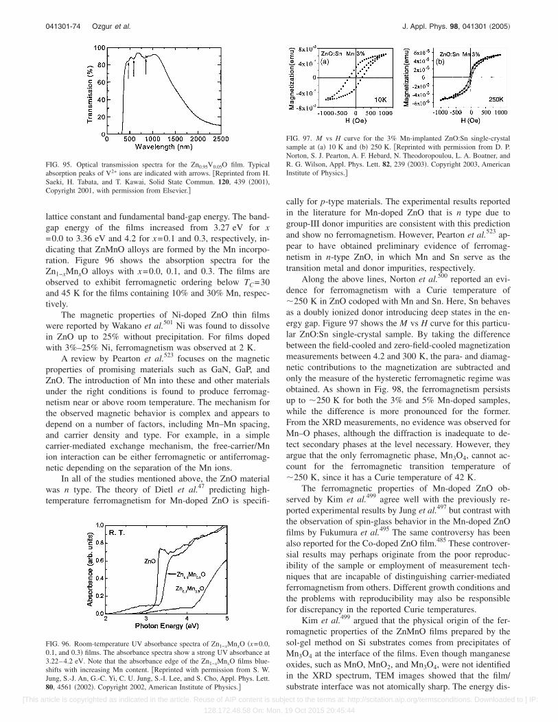
lattice constant and fundamental band-gap energy. The band-gap energy of the films increased from 3.27 eV for x=0.0 to 3.36 eV and 4.2 for x=0.1 and 0.3, respectively, in-dicating that ZnMnO alloys are formed by the Mn incorpo-ration. Figure 96 shows the absorption spectra for theZn1−xMnxO alloys with x=0.0, 0.1, and 0.3. The films areobserved to exhibit ferromagnetic ordering below TC=30and 45 K for the films containing 10% and 30% Mn, respec-tively.
The magnetic properties of Ni-doped ZnO thin filmswere reported by Wakano et al.501 Ni was found to dissolvein ZnO up to 25% without precipitation. For films dopedwith 3%–25% Ni, ferromagnetism was observed at 2 K.
A review by Pearton et al.523 focuses on the magneticproperties of promising materials such as GaN, GaP, andZnO. The introduction of Mn into these and other materialsunder the right conditions is found to produce ferromag-netism near or above room temperature. The mechanism forthe observed magnetic behavior is complex and appears todepend on a number of factors, including Mn–Mn spacing,and carrier density and type. For example, in a simplecarrier-mediated exchange mechanism, the free-carrier/Mnion interaction can be either ferromagnetic or antiferromag-netic depending on the separation of the Mn ions.
In all of the studies mentioned above, the ZnO materialwas n type. The theory of Dietl et al.47 predicting high-temperature ferromagnetism for Mn-doped ZnO is specifi-
cally for p-type materials. The experimental results reportedin the literature for Mn-doped ZnO that is n type due togroup-III donor impurities are consistent with this predictionand show no ferromagnetism. However, Pearton et al.523 ap-pear to have obtained preliminary evidence of ferromag-netism in n-type ZnO, in which Mn and Sn serve as thetransition metal and donor impurities, respectively.
Along the above lines, Norton et al.500 reported an evi-dence for ferromagnetism with a Curie temperature of�250 K in ZnO codoped with Mn and Sn. Here, Sn behavesas a doubly ionized donor introducing deep states in the en-ergy gap. Figure 97 shows the M vs H curve for this particu-lar ZnO:Sn single-crystal sample. By taking the differencebetween the field-cooled and zero-field-cooled magnetizationmeasurements between 4.2 and 300 K, the para- and diamag-netic contributions to the magnetization are subtracted andonly the measure of the hysteretic ferromagnetic regime wasobtained. As shown in Fig. 98, the ferromagnetism persistsup to �250 K for both the 3% and 5% Mn-doped samples,while the difference is more pronounced for the former.From the XRD measurements, no evidence was observed forMn–O phases, although the diffraction is inadequate to de-tect secondary phases at the level necessary. However, theyargue that the only ferromagnetic phase, Mn3O4, cannot ac-count for the ferromagnetic transition temperature of�250 K, since it has a Curie temperature of 42 K.
The ferromagnetic properties of Mn-doped ZnO ob-served by Kim et al.499 agree well with the previously re-ported experimental results by Jung et al.497 but contrast withthe observation of spin-glass behavior in the Mn-doped ZnOfilms by Fukumura et al.495 The same controversy has beenalso reported for the Co-doped ZnO film.485 These controver-sial results may perhaps originate from the poor reproduc-ibility of the sample or employment of measurement tech-niques that are incapable of distinguishing carrier-mediatedferromagnetism from others. Different growth conditions andthe problems with reproducibility may also be responsiblefor discrepancy in the reported Curie temperatures.
Kim et al.499 argued that the physical origin of the fer-romagnetic properties of the ZnMnO films prepared by thesol-gel method on Si substrates comes from precipitates ofMn3O4 at the interface of the films. Even though manganeseoxides, such as MnO, MnO2, and Mn3O4, were not identifiedin the XRD spectrum, TEM images showed that the film/substrate interface was not atomically sharp. The energy dis-
FIG. 95. Optical transmission spectra for the Zn0.95V0.05O film. Typicalabsorption peaks of V2+ ions are indicated with arrows. �Reprinted from H.Saeki, H. Tabata, and T. Kawai, Solid State Commun. 120, 439 �2001�,Copyright 2001, with permission from Elsevier.�
FIG. 96. Room-temperature UV absorbance spectra of Zn1−xMnxO �x=0.0,0.1, and 0.3� films. The absorbance spectra show a strong UV absorbance at3.22–4.2 eV. Note that the absorbance edge of the Zn1−xMnxO films blue-shifts with increasing Mn content. �Reprinted with permission from S. W.Jung, S.-J. An, G.-C. Yi, C. U. Jung, S.-I. Lee, and S. Cho, Appl. Phys. Lett.80, 4561 �2002�. Copyright 2002, American Institute of Physics.�
FIG. 97. M vs H curve for the 3% Mn-implanted ZnO:Sn single-crystalsample at �a� 10 K and �b� 250 K. �Reprinted with permission from D. P.Norton, S. J. Pearton, A. F. Hebard, N. Theodoropoulou, L. A. Boatner, andR. G. Wilson, Appl. Phys. Lett. 82, 239 �2003�. Copyright 2003, AmericanInstitute of Physics.�
041301-74 Ozgur et al. J. Appl. Phys. 98, 041301 �2005�
[This article is copyrighted as indicated in the article. Reuse of AIP content is subject to the terms at: http://scitation.aip.org/termsconditions. Downloaded to ] IP:
128.172.48.58 On: Mon, 19 Oct 2015 20:45:44

persive spectroscopy �EDS� measurements performed on theinterfacial region showed significant amounts of Mn com-pared to the region away from the interface. MnO and MnO2
cannot be regarded as possible candidates for the ferromag-netic precipitates at the interface since they are both antifer-romagnetic below 116 and 84 K, respectively.497 However,ferromagnetic long-range order has been observed forMn3O4.524 The Mn:O ratio measured at the interface �closeto 3:4� also indicates that Mn3O4 is the most probable causefor the observed ferromagnetism in the ZnMnO films.
Rode et al.487 investigated the microstructure and themagnetic properties of cobalt-substituted ZnO thin films de-posited on sapphire �0001� substrates by pulsed-laser depo-sition. Films with 25% of Co were ferromagnetic at roomtemperature with clear out-of-plane anisotropy. It was foundout that lower growth pressures result in more oxygen vacan-cies, inducing free electrons which mediate the ferromag-netic exchange interactions as suggested by Sato andKatayama-Yoshida.512 Besides the ferromagnetic behavior,evidence of an out-of-plane easy magnetization axis wasclearly observed. The authors claim that this observed crystalanisotrophy supports the assumption that the ferromagnetismarises from the �Zn,Co�O phase.
The dependence of ZnMnO band gap on Mn content hasbeen studied also by Tiwari et al.525 Due to the nonequilib-rium nature of the laser-material interaction, high Mn con-
tents �x=0.36� could be introduced using PLD. Optical trans-mittance showed an increase in the insulating band gap �Eg�with increase in Mn atomic fraction x following the relationEg=3.270+2.760x−4.988x2 eV. dc magnetization measure-ments on these samples showed the paramagnetic nature ofthe ZnMnO system. Figure 99�a� shows the optical absor-bance spectra of the ZnMnO films. As seen from this figure,the absorption edge moves towards the higher-energy side asthe Mn content increases. This indicates the increase in theband gap of the system. Significant amount of midgap ab-sorption is also observed in these samples. This phenomenonwas also reported in earlier studies and was attributed to thecharge-transfer transition between donor and acceptor ioniza-tion levels of Mn ions and the band continuum.495,497
Cheng and Chien526 also found no ferromagnetic order-ing in Mn-doped ZnO thin films. The magnetic properties ofa Zn0.93Mn0.07O film were measured by a SQUID magneto-
FIG. 98. Temperature dependence of the difference between field-cooledand zero-field-cooled magnetizations for �a� 3% and �b� 5% implanted Mnconcentrations in n-type ZnO:Sn single crystal. �Reprinted with permissionfrom D. P. Norton, S. J. Pearton, A. F. Hebard, N. Theodoropoulou, L. A.Boatner, and R. G. Wilson, Appl. Phys. Lett. 82, 239 �2003�. Copyright2003, American Institute of Physics.�
FIG. 99. �a� Optical absorbance spectra of Zn1−xMnxO films. a, b, c, d, ande correspond to x=0.01, 0.05, 0.12, 0.18, and 0.25, respectively. �b� Varia-tion of the band gap of Zn1−xMnxO films with x. The data fit well in asecond-order polynomial equation Eg=3.270+2.762x−4.988x2 �solid line�.�Reprinted with permission from A. Tiwari, C. Jin, A. Kvit, D. Kumar, J. F.Muth, and J. Narayan, Solid State Commun. 121, 371 �2002�. Copyright2002, American Institute of Physics.�
041301-75 Ozgur et al. J. Appl. Phys. 98, 041301 �2005�
[This article is copyrighted as indicated in the article. Reuse of AIP content is subject to the terms at: http://scitation.aip.org/termsconditions. Downloaded to ] IP:
128.172.48.58 On: Mon, 19 Oct 2015 20:45:44

meter at various temperatures with fields up to 5 T. The Au-ger electron spectroscopy showed homogeneous distributionof Mn in the film and the magnetic properties verified thatthe film was paramagnetic. The magnetic properties of Mn-doped ZnO are expected to be strongly influenced by thecarrier type �p or n� and carrier density.47,512 However, thesecharacteristics of Mn-doped ZnO films are not well knownexperimentally at present.
In contrast to earlier work �Fukumura et al.496 found aspin-glass behavior, Jung et al.497 observed ferromagneticordering with a TC�45 K, Tiwari et al.525 ruled out theroom-temperature ferromagnetism, and Cheng and Chien526
discovered paramagnetic behavior� Sharma et al.488 claimedto have confirmed the ferromagnetism in Mn-doped ZnO. Inthis particular report room-temperature ferromagnetism wasobserved in bulk pellets, thin films, and powder form of Mn-doped ZnO. The authors attributed their achievement to theunique feature of their sample preparation having to do withlow-temperature processing. When standard high-temperature �T=700 °C� methods were used, the sampleswere found to exhibit clustering and were not ferromagneticat room temperature. No trace of any secondary phase orother impurities was found in ferromagnetic resonance�FMR�, EDS, and also x-ray-diffraction measurements.However, the average local Mn concentration in bulk pellets��0.3% � determined by the EDS technique was found to bemuch lower than the nominal composition �2%�. The FMRdata suggest TC well above 425 K. Sintering the pelletsabove 700 °C completely suppressed ferromagnetism to be-low room temperature. Mn-doped ZnO became inhomoge-neous with the increase in sintering temperature, probablybecause of Mn clustering or formation of other phases suchas Zn2Mn3O8, ZnMn3O7, and Mn2O3. The increased numberof free electrons and the onset of clustering of Mn, in thehigh-temperature processed samples, deviate the system farfrom the ideal Mn-doped ZnO. Again, the field is riddledwith controversy which may dissipate in time.
Ramachandran et al.489 observed room-temperature fer-romagnetism in Zn0.9Co0.1O epitaxial films grown by pulsed-laser deposition. Electron-energy-loss spectroscopy �EELS�was used to determine the oxidation state at various points inthe films. The oxidation state of cobalt was found not tochange across the film, and a +2 oxidation state was inducedwhich suggests a uniform substitution of Zn by Co. Atomic-scale structural characterization including high-resolutionTEM, scanning transmission electron microscopy-atomicnumber �STEM-Z� contrast, and EELS was done to provideevidence for the absence of any nanosized clusters or secondphase. XRD, TEM, and STEM-Z contrast measurements alsosupported the premise that Co nanoclusters and secondphases could not be the cause for the observed room-temperature ferromagnetism.
In addition, optical measurements on a Zn0.9Co0.1Osample grown at 500 °C revealed three absorption edges at658, 616, and 568 nm, which were correlated with the d-dtransitions of the tetrahedrally coordinated Co2+ ions �Fig.100�. Using the results from both optical and structural mea-surements Ramachandran et al.489 concluded that the room-
temperature ferromagnetism is an inherent property of thematerial caused by the presence of cobalt in high-spin con-figuration in a tetrahedral crystal field.
Lin et al.490 reported that additional Cu doping into bulkZn0.98Co0.02O is essential to achieve room-temperature ferro-magnetism. From the results of x-ray and EDX mapping, theZn0.97Cu0.01Co0.02O film grown by standard solid-state reac-tion method was observed to have a homogeneous distribu-tion with no secondary phases.
However, because of the lack of detailed microstructuralcharacterization in the reports mentioned above, there is stilla good deal of controversy over the fate of these magneticimpurities �nanosize clusters/precipitates and/or individualatoms in substitutional sites� and whether the magnetic be-havior is an intrinsic property of the films or due to thepresence of nanoclusters of a magnetic phase or a combina-tion of both. Most experimental reports concerning room-temperature ferromagnetism in DMS employ x-ray diffrac-tion, selected-area diffraction patterns, transmission electronmicroscopy, photoemission, or x-ray absorption to determinewhether the magnetic atoms are substituting for one of thelattice constituents to form an alloy. Given the level of dilu-tion of the magnetic atoms, it is often very difficult to cat-egorically determine the origin of the ferromagnetism. Forexample, a recent study500 reported the presence of Co nano-clusters in Co+-implanted ZnO �exhibiting RT ferromag-netism�, but did not preclude the possibility of the compo-nent of the magnetic property due to Co substitution of theZn in ZnO lattice. In addition, there are still extreme varia-tions in the reported magnetic behavior with some films ex-hibiting only paramagnetism and even those with ferromag-netism showing a wide range of apparent Curie temperatures.In short, the origin of this ferromagnetism is not yet clear.
VIII. BAND-GAP ENGINEERING
A crucial step in designing modern optoelectronic de-vices is the realization of band-gap engineering to create bar-rier layers and quantum wells in device heterostructures. Inorder to realize such optoelectronic devices, two important
FIG. 100. Optical transmission spectrum of the Zn0.9Co0.1O film grown at500 °C. The absorption edges at 658, 616, and 568 nm are indicated as 1, 2,and 3, respectively. �Reprinted with permission from S. Ramachandran, A.Tiwari, and J. Narayan, Appl. Phys. Lett. 84, 5255 �2004�. Copyright 2004,American Institute of Physics.�
041301-76 Ozgur et al. J. Appl. Phys. 98, 041301 �2005�
[This article is copyrighted as indicated in the article. Reuse of AIP content is subject to the terms at: http://scitation.aip.org/termsconditions. Downloaded to ] IP:
128.172.48.58 On: Mon, 19 Oct 2015 20:45:44

requirements should be satisfied; one is p-type doping ofZnO as discussed previously, and the other is modulation ofthe band gap. While p-type doping of ZnO is under intensivestudy, the latter has been demonstrated by the developmentof MgxZn1−xO �Refs. 527–540 and CdyZn1−yOalloys,537,541–547 allowing modulation of band gap in a widerange. The energy gap Eg�x� of the ternary semiconductorAxZn1−xO �where A=Mg or Cd� is determined by the follow-ing equation:548
Eg�x� = �1 − x�EZnO + xEAO − bx�1 − x� , �35�
where b is the bowing parameter and EAO and EZnO are theband-gap energies of compounds AO and ZnO, respectively.The bowing parameter b depends on the difference in elec-tronegativities of the end binaries ZnO and AO. The bandgap can be increased �decreased� by incorporating Mg �Refs.528–530� �Cd �Refs. 541, 542, and 545�� into ZnO.
Figure 101 shows the a lattice parameter as a function ofroom-temperature Eg values in CdyZn1−yO and MgxZn1−xOalloys. A �Cd,Zn�O/ �Mg,Zn�O superlattice �SL�, having aperfect lattice match between layers and a maximum barrierheight of 0.09 eV, can be obtained by choosing an appropri-ate combination of Cd and Mg concentrations, because botha parameters are monotonically increasing functions of alloycomposition. This is a major advantage when compared to�In,Ga�N/ �Al,Ga�N SLs since in the case of wurtzite struc-ture, if the lattice constant of the well layer differs from thatof the barrier layer, strain field exists inside the well layerswhich causes polarization charge. The same parametric plotsfor �In,Ga�N and �Al,Ga�N are shown by the dashed curvesin Fig. 101.
A. MgxZn1−xO alloy
MgxZn1−xO alloy has been considered as a suitable ma-terial for the barrier layers in ZnO/ �Mg,Zn�O superlatticestructures537 because alloying ZnO with MgO �Eg�7.7 eV�enables widening of band gap of ZnO. According to thephase diagram of the ZnO–MgO binary system, the thermo-
dynamic solid solubility of MgO in ZnO is less than4 mol %.549 In addition, ZnO has a wurtzite structureal �a=3.24 Šand c=5.20 �, while MgO has a cubic structure�a=4.24 �.
One of the reports on the synthesis of MgxZn1−xO with aMg content of up to 33% was by Ohtomo et al.527 by PLD. Itwas found that MgO segregates in the wurtzite MgZnO lat-tice above 33% of Mg content, limiting the maximum bandgap to 3.9 eV. XRD studies show that the a-axis lengthgradually increases and the c-axis length decreases with in-creasing Mg content, and therefore the cell volume is hardlychanged. Figure 102 shows the transmittance spectra mea-sured at room temperature. The band gap Eg linearly in-creases with x up to 4.15 eV for 0�x�0.36 and saturates athigher Mg concentrations due to MgO segregation �Fig. 102,inset�. This indicates that MgxZn1−xO is a suitable materialfor barrier layers in ZnO/ �Mg,Zn�O heterostructures with aband-gap offset up to 0.85 eV. Linear dependence of Eg on xup to x=0.36 shows that the bowing parameter b is 0 eV,although a final declaration must wait for additional andmore refined experiments. Increasing the Mg compositionfurther resulted in MgxZn1−xO films in metastable cubicphase with band gaps above 5.0 eV.529 The Mg contentstrongly depended on the growth temperature, consequentlyshowing strong dependence of band-gap energy on thegrowth temperature ranging from room temperature to750 °C.
Gruber et al.530 grew MgZnO epilayers and ZnO–MgZnO quantum well structures by MOVPE and studiedtheir properties. All the samples were grown on GaN/sapphire templates in a horizontal flow reactor at a growthtemperature of 600 °C. A 1-�m ZnO buffer was also in-cluded to improve structural quality. Diethylzinc �DEZn�,bis� methylcyclopentadienyl�magnesium �MeCp2Mg�, andnitrous oxide were used as the zinc, magnesium, and oxygenprecursors, respectively. The Mg incorporation into the ZnOhost material and its effect on the band gap was determinedby PL measurements. An increase of 200 meV in the bandgap at a Mg concentration of 10% has been achieved, andusing MgZnO as the barrier material, ZnO–MgZnO quantumwells with different well widths were grown. The quantum
FIG. 101. Optical and structural properties of CdyZn1−yO and MgxZn1−xOalloy films mapped out in a plane of a-axis length and room-temperatureband-gap energy. The same curves for �In, Ga�N and �Al, Ga�N alloys arealso shown. The alloy compositions are shown on the top axis. �Reprintedwith permission from T. Makino, Y. Segawa, M. Kawasaki, A. Ohtomo, R.Shiroki, K. Tamura, T. Yasuda, and H. Koinuma, Appl. Phys. Lett. 78, 1237�2001�. Copyright 2001, American Institute of Physics.�
FIG. 102. Transmittance spectra of MgxZn1−xO films measured at roomtemperature. The inset shows the band gap �Eg� determined from the spectraassuming an �2� �h�−Eg� dependence, where � and h� are the absorptioncoefficient and the photon energy, respectively. �Reprinted with permissionfrom A. Ohtomo, M. Kawasaki, T. Koida, K. Masubuchi, and H. Koinuma,Appl. Phys. Lett. 72, 2466 �1998�. Copyright 1998, American Institute ofPhysics.�
041301-77 Ozgur et al. J. Appl. Phys. 98, 041301 �2005�
[This article is copyrighted as indicated in the article. Reuse of AIP content is subject to the terms at: http://scitation.aip.org/termsconditions. Downloaded to ] IP:
128.172.48.58 On: Mon, 19 Oct 2015 20:45:44
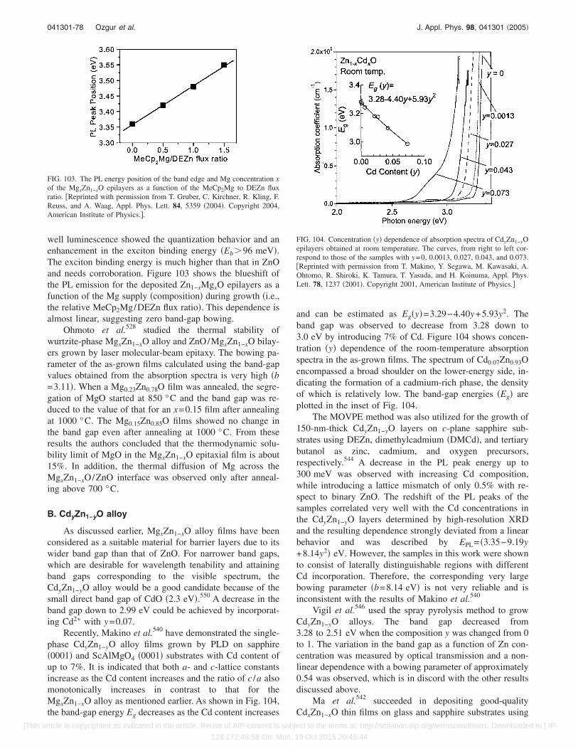
well luminescence showed the quantization behavior and anenhancement in the exciton binding energy �Eb�96 meV�.The exciton binding energy is much higher than that in ZnOand needs corroboration. Figure 103 shows the blueshift ofthe PL emission for the deposited Zn1−xMgxO epilayers as afunction of the Mg supply �composition� during growth �i.e.,the relative MeCp2Mg/DEZn flux ratio�. This dependence isalmost linear, suggesting zero band-gap bowing.
Ohmoto et al.528 studied the thermal stability ofwurtzite-phase MgxZn1−xO alloy and ZnO/MgxZn1−xO bilay-ers grown by laser molecular-beam epitaxy. The bowing pa-rameter of the as-grown films calculated using the band-gapvalues obtained from the absorption spectra is very high �b=3.11�. When a Mg0.23Zn0.78O film was annealed, the segre-gation of MgO started at 850 °C and the band gap was re-duced to the value of that for an x=0.15 film after annealingat 1000 °C. The Mg0.15Zn0.85O films showed no change inthe band gap even after annealing at 1000 °C. From theseresults the authors concluded that the thermodynamic solu-bility limit of MgO in the MgxZn1−xO epitaxial film is about15%. In addition, the thermal diffusion of Mg across theMgxZn1−xO/ZnO interface was observed only after anneal-ing above 700 °C.
B. CdyZn1−yO alloy
As discussed earlier, MgxZn1−xO alloy films have beenconsidered as a suitable material for barrier layers due to itswider band gap than that of ZnO. For narrower band gaps,which are desirable for wavelength tenability and attainingband gaps corresponding to the visible spectrum, theCdyZn1−yO alloy would be a good candidate because of thesmall direct band gap of CdO �2.3 eV�.550 A decrease in theband gap down to 2.99 eV could be achieved by incorporat-ing Cd2+ with y=0.07.
Recently, Makino et al.540 have demonstrated the single-phase CdyZn1−yO alloy films grown by PLD on sapphire�0001� and ScAlMgO4 �0001� substrates with Cd content ofup to 7%. It is indicated that both a- and c-lattice constantsincrease as the Cd content increases and the ratio of c /a alsomonotonically increases in contrast to that for theMgxZn1−xO alloy as mentioned earlier. As shown in Fig. 104,the band-gap energy Eg decreases as the Cd content increases
and can be estimated as Eg�y�=3.29−4.40y+5.93y2. Theband gap was observed to decrease from 3.28 down to3.0 eV by introducing 7% of Cd. Figure 104 shows concen-tration �y� dependence of the room-temperature absorptionspectra in the as-grown films. The spectrum of Cd0.07Zn0.93Oencompassed a broad shoulder on the lower-energy side, in-dicating the formation of a cadmium-rich phase, the densityof which is relatively low. The band-gap energies �Eg� areplotted in the inset of Fig. 104.
The MOVPE method was also utilized for the growth of150-nm-thick CdyZn1−yO layers on c-plane sapphire sub-strates using DEZn, dimethylcadmium �DMCd�, and tertiarybutanol as zinc, cadmium, and oxygen precursors,respectively.544 A decrease in the PL peak energy up to300 meV was observed with increasing Cd composition,while introducing a lattice mismatch of only 0.5% with re-spect to binary ZnO. The redshift of the PL peaks of thesamples correlated very well with the Cd concentrations inthe CdyZn1−yO layers determined by high-resolution XRDand the resulting dependence strongly deviated from a linearbehavior and was described by EPL= �3.35−9.19y+8.14y2� eV. However, the samples in this work were shownto consist of laterally distinguishable regions with differentCd incorporation. Therefore, the corresponding very largebowing parameter �b=8.14 eV� is not very reliable and isinconsistent with the results of Makino et al.540
Vigil et al.546 used the spray pyrolysis method to growCdyZn1−yO alloys. The band gap decreased from3.28 to 2.51 eV when the composition y was changed from 0to 1. The variation in the band gap as a function of Zn con-centration was measured by optical transmission and a non-linear dependence with a bowing parameter of approximately0.54 was observed, which is in discord with the other resultsdiscussed above.
Ma et al.542 succeeded in depositing good-qualityCdxZn1−xO thin films on glass and sapphire substrates using
FIG. 103. The PL energy position of the band edge and Mg concentration xof the MgxZn1−xO epilayers as a function of the MeCp2Mg to DEZn fluxratio. �Reprinted with permission from T. Gruber, C. Kirchner, R. Kling, F.Reuss, and A. Waag, Appl. Phys. Lett. 84, 5359 �2004�. Copyright 2004,American Institute of Physics.�.
FIG. 104. Concentration �y� dependence of absorption spectra of CdyZn1−yOepilayers obtained at room temperature. The curves, from right to left cor-respond to those of the samples with y=0, 0.0013, 0.027, 0.043, and 0.073.�Reprinted with permission from T. Makino, Y. Segawa, M. Kawasaki, A.Ohtomo, R. Shiroki, K. Tamura, T. Yasuda, and H. Koinuma, Appl. Phys.Lett. 78, 1237 �2001�. Copyright 2001, American Institute of Physics.�
041301-78 Ozgur et al. J. Appl. Phys. 98, 041301 �2005�
[This article is copyrighted as indicated in the article. Reuse of AIP content is subject to the terms at: http://scitation.aip.org/termsconditions. Downloaded to ] IP:
128.172.48.58 On: Mon, 19 Oct 2015 20:45:44
the dc reactive magnetron sputtering method. The samplesexhibited good transmittance �over 85%� in the visible spec-tral range and a redshift was observed in the PL with increas-ing Cd composition. The films with x�0.53 have structuresof pure CdxZn1−xO with the c axis perpendicular to the sub-strate surface, while the films with x=0.77 were mixtures ofa hexagonal ZnO phase and a cubic CdO phase. The bandgaps of the Zn1−xCdxO alloy films �0�x�0.53� could benonlinearly tuned from 3.28 to 2.65 eV with the Cd contentsfrom x=0 to x=0.53.
IX. PROCESSING, DEVICES, ANDHETEROSTRUCTURES
A. Ohmic contacts to ZnO
An Ohmic contact can be defined as having a linear andsymmetric current-voltage relationship for both positive andnegative voltages and is so important for carrying electricalcurrent into and out of the semiconductor, ideally with noparasitic resistance. It is well known that parasitic resistance,in the form of contact resistance, is one of the major ob-stacles in realizing long-lifetime operation of optical andelectrical devices. The major loss of device performance isoften caused by high-resistance metal-semiconductor Ohmiccontacts through thermal stress and or contact failure.551
Thus, in order to attain high-performance ZnO-based opticaland electrical devices, it is essential to achieve Ohmic con-tacts that have both low resistance and are thermally stableand reliable. This can be achieved either by performing sur-face preparation to reduce the metal-semiconductor barrierheight which would allow to increase carrier tunneling prob-ability or by increasing the effective carrier concentration ofthe surface perhaps taking advantage of oxygen loss.552–555
Ohmic-contact metallization should be one of the maingoals in improving device performance which plays an im-portant role in device technology.553 Although a low-resistance Ohmic contact on wide-band-gap semiconductorscan be obtained by thermal annealing, surface roughness andstructural degradation of the interface can be induced duringthe thermal annealing process,556,557 resulting in poor deviceperformance and reliability.558 Therefore, it may in some in-stances be preferable to develop low-resistance Ohmic con-tacts without the use of a thermal annealing process. For thatreason, in the case of Ohmic-contact technology, nonalloyed
Ohmic contacts with low specific contact resistance arepreferred,555,559–561 particularly for shallow junction and low-voltage devices since they provide smooth metal-semiconductor interfaces resulting from the limited interfacereaction. However, Ohmic-contact metallization technologyin ZnO has not been explored extensively until now, a pic-ture which still holds in these early stages of development.
Lee et al.561 have achieved low-resistance and nonal-loyed Ohmic contacts to epitaxially grown n-ZnO formed byexposing n-ZnO to an inductively coupled hydrogen and ar-gon plasmas. It has been shown that the specific contactresistivity562 of the resulting Ohmic contacts drastically de-creased from 7.3�10−3 to 4.3�10−5 � cm2 by hydrogen-plasma treatment using Ti/Au metallization schemes. Thespecific contact resistivity of the Ar-plasma-treated samplehas also decreased to 5.0�10−4 � cm2 which is lower by anorder of the magnitude compared to that of the as-grownsample, and this decrease has been attributed to the forma-tion of shallow donor by ion bombardment leading to oxygenvacancies on the ZnO surface. This result is comparable tothe result reported by Kim et al.,556 using the same metalli-zation schemes after annealing at 300 °C. The specific con-tact resistance was measured to be 2�10−2 � cm2 for theas-deposited contact, and 2�10−4 and 1�10−3 � cm2 forthe contacts annealed at 300 and 500 °C, respectively.556 An-nealing at 300 °C for 1 min resulted in high-quality Ohmiccontacts, leading to a reduction by two orders of magnitudein specific contact resistance compared to the as-depositedcontacts. This enhancement has been attributed to the com-bined effects of the increases in the carrier concentrationnear the ZnO layer surface and the contact area.
Kim et al.559 have investigated nonalloyed Al and Al/PtOhmic contacts on n-type ZnO and found that the I-V char-acteristics of the as-deposited Al and Al/Pt contacts onn-type ZnO reveal linear behavior with specific contact re-sistivities of 8.0�10−4 and 1.2�10−5 � cm2, respectively.Pt overlayer on Al contact, compared to the case without theoverlayer, has resulted in a large reduction in the specificcontact resistivity on n-type ZnO. This reduction has been
FIG. 105. The experimental specific contact resistances as a function oftemperature for unintentionally doped �open circles� and heavily Ga-doped�solid circles� ZnO �after Sheng et al. �Ref. 555��.
FIG. 106. Specific contact resistance vs carrier concentration of the as-deposited Ohmic contact measured at 30 °C, and at 30 and 200 °C, afterannealing at 200 °C for 1 min. �Reprinted with permission from K. Ip, Y.Heo, K. Balik, D. P. Norton, S. J. Pearton, and F. Ren, Appl. Phys. Lett. 84,544 �2004�. Copyright 2004, American Institute of Physics.�
041301-79 Ozgur et al. J. Appl. Phys. 98, 041301 �2005�
[This article is copyrighted as indicated in the article. Reuse of AIP content is subject to the terms at: http://scitation.aip.org/termsconditions. Downloaded to ] IP:
128.172.48.58 On: Mon, 19 Oct 2015 20:45:44
attributed to the prevention of surface oxide layer �Al–O� bythe Pt metal. A nonalloyed In-based Ohmic contact whichhas been formed on a hydrothermally grown n-type ZnOsubstrate by KrF excimer laser irradiation with 0.3 J /cm2
and metal deposition without any impurity doping has beeninvestigated by Akane et al.560 The In-deposited laser-irradiated sample exhibited Ohmic behavior with a resistivityof 7�10−1 � cm2. The same, however, was not the case forunirradiated samples with and without the contact metalwhich indicates that the laser irradiation enables current con-duction into the n-type ZnO substrate. A decrease in the cur-rent density was also observed after 5-min postannealing at300 °C, which resulted in degradation of the electrical prop-erties. In addition, Ti/Au contacts showed thermal degrada-tion after annealing at temperatures in excess of 300 °C�Ref. 556� and the same behavior was observed by Akane etal.560 for In Ohmic contacts annealed at 300 °C for 5 min.Kim et al.563 have investigated Ru Ohmic contacts to n-typeZnO. In spite of the fact that the as-deposited Ru contactyielded a specific contact resistivity of 2.1�10−3 � cm2, thecontact annealed at 700 °C for 1 min yielded a specific con-tact resistance of 3.2�10−5 � cm2, about two orders of mag-nitude smaller compared to the as-deposited one withoutshowing any electrical and thermal degradation observed inthe case of Ti/Au and In contacts. It was also shown thatprolonged annealing �10 min� at the same temperaturecaused no significant electrical and surface morphology deg-radation, indicating that Ru is suitable for high-temperatureZnO devices.563 The surface modification �by means of ap-plying a high-energy beam of Ga ions before the metal depo-sition� and Pt direct-write metal deposition approach havebeen applied to unintentionally doped n-type ZnO films andlinear Ohmic-contact characteristics have beenachieved.553,564 The specific contact resistivity values forsurface-modification doses Ds1=1�1017 cm−2, Ds2=3�1017 cm−2, and Ds3=3�1016 cm−2 have been obtained as3.1, 3.3, and 3.7�10−4 � cm2, respectively. These values areone order of magnitude lower than the lowest specific con-tact resistance �4.1�10−3 � cm2� for Pt direct write withoutsurface-modified contacts.553,564
Sheng et al.555 have fabricated Al/Au nonalloyed Ohmiccontacts on epitaxial MgxZ1−xO �0�x�0.34� making use ofthe low barrier height of Al on ZnO.565 The specific contactresistance has been investigated as a function of Mg compo-sition in ZnO films and it has been shown that with increas-ing Mg composition �increasing band gap� the specific con-tact resistance increased from 2.5�10−5 to 9.1�10−3 � cm2. This represents an increase of more than twoorders of magnitude as compared to a ZnO sample with anelectron concentration of 1.6�1017 cm−3. The experimentalspecific contact resistances as a function of temperature forunintentionally and heavily Ga-doped ZnO have been givenin Fig. 105. It has been shown that if the electron concentra-tions increased �by Ga doping during the growth�, the spe-cific contact resistivity would decrease because of the in-creased tunneling. Another observation was that, even if thespecific contact resistivity did not change as a function of
temperature, the heavily doped ZnO showed lower specificcontact resistivity than that for the unintentionally dopedZnO.555
Ip et al.566 could obtain a minimum specific contact re-sistance of 6�10−4 � cm2 for Ti/Al/Pt/Au contacts on un-doped �n=1017 cm−3� bulk ZnO. The contacts did not showOhmic behavior in the as-deposited state and reached theirminimum resistance after 250 °C annealing. This value wasessentially independent of the surface cleaning procedureemployed, including sequential solvent cleaning or H2
plasma exposure. Higher annealing temperatures degradedthe specific contact resistance, and Auger electron spectros-copy depth profiling revealed increasing intermixing of themetal layers and reaction of Ti with ZnO. The Al was ob-served to outdiffuse to the surface at temperatures as low as350 °C, and the contact metallization was almost completelyintermixed by 600 °C.
The carrier-concentration dependence of theTi/Al/Pt/Au Ohmic-contact resistance on P-doped n-typeZnO thin films �7.5�1015−1.5�1020 cm−3� has also beenreported.567,568 Even in the as-deposited state, low specificcontact resistances in the range from 3�10−4 to 8�10−7 � cm2 were observed. The lowest specific contact re-sistance of 8�10−7 � cm2 for nonalloyed Ohmic contactswas achieved in the sample with a carrier concentration of1.5�1020 cm−3 when measured at 30 °C. In the annealedsamples, minimum specific contact resistances of 3.9�10−7
and 2.2�10−8 � cm2 were obtained in the samples with car-rier concentrations of 6.0�1019 cm−3 measured at 30 °Cand 2.4�1018 cm−3 measured at 200 °C, respectively. Fig-ure 106 shows the dependence of specific contact resistanceon carrier concentration for the as-deposited and annealedcontacts. Temperature-dependent measurements showed thatthe dominant transport mechanisms were tunneling in thecontacts for the most highly doped films and thermionicemission for the more lightly doped films. As in the bulkZnO case, Auger electron spectroscopy detected Ti–O inter-facial reaction and intermixing between Al and Pt at 200 °C.The significant changes in morphology even for low-temperature �200 °C� anneals suggest that more thermallystable contact schemes should be investigated.
Some of the various Ohmic-contact metallizationschemes to n-type ZnO are summarized in Table XVIII to-gether with carrier concentration, specific contact resistance,and method used to measure the specific contact resistivity.Recently, Al,569–571 Al/Au,572 Ti,573 In,574 InGa �Ref. 575�metallizations were also used to obtain Ohmic contacts. De-spite some progress in ZnO-based devices, there is still dif-ficulty in the reproducible growth of p-type ZnO and verylimited information about Ohmic contacts to p-type ZnOmaterial.475,576,577 For that reason, the Ohmic contact to thep-type ZnO material will not be discussed here.
B. Schottky contacts to ZnO
In spite of the fact that high-quality Schottky contactsare critical for ZnO device applications, there is little infor-mation about the Schottky contacts on ZnO to date. Thechemical reactions between the metal and the semiconductor,
041301-80 Ozgur et al. J. Appl. Phys. 98, 041301 �2005�
[This article is copyrighted as indicated in the article. Reuse of AIP content is subject to the terms at: http://scitation.aip.org/termsconditions. Downloaded to ] IP:
128.172.48.58 On: Mon, 19 Oct 2015 20:45:44

the surface states, the contaminants, the defects in the surfacelayer, and the diffusion of the metal into the semiconductorare well-known problems in the formation of Schottky con-tacts. For instance, in the case of ZnO Al is expected toproduce the most dissociated cations �Zn� in ZnO because ofits strong reaction with anions �O� in ZnO. This results inlow barrier height and leakage current.
To create Schottky barrier with undoped ZnO, a highwork function can be applied to the surface of a ZnO crystal.Although many publications575,578 show that Au has someserious problems at high temperatures ��340 K�, it haswidely been applied to ZnO to form Schottkybarriers.573–575,578–580 Other metals used for the same purposeare Ag,569–571,574,578,579 Pd,580,581 and Pt.582–585 It has beenfound that all these reactive metals form relatively highSchottky barriers of 0.6–0.84 eV to the n-type ZnO.
Although Schottky barrier heights were reported byMead579 for various metal contacts on vacuum-cleavedn-type ZnO surfaces in 1965, the thermal stability of theSchottky diodes fabricated on ZnO has not been extensivelystudied. It was observed that Au Schottky contacts resultedin poor current-voltage characteristics and degraded easilywith thermal cycling of the samples.571 This study showedthat the thermal stability of Ag Schottky contacts was betterthan that of Au Schottky contacts. Mead579 measured barrierheights for Ag and Au Schottky contacts as 0.68 and0.65 eV, respectively. Neville and Mead580 investigatedsurface-barrier systems consisting of Au and Pd on bulkZnO, which were chemically prepared by concentrated phos-phoric acid, concentrated HCl, and organic solvents andshowed an ideality factor very close to unity �1.05�. Koppa etal.573 have investigated Au Schottky contacts on n-type ZnOwafers which were clean, stoichiometric, highly ordered, and
smooth after exposure to an O2/He plasma. Significant im-provement in the I-V characteristics of as-deposited AuSchottky contacts was observed relative to those characteris-tics measured for similar contacts deposited on the same sur-faces of the as-received wafers. Compared to the contacts onthe as-received material which showed microampere leakagecurrents and ideality factors of n�2, contacts on plasma-cleaned wafers cooled in vacuum showed leakage current ofabout 36 nA at −4 V, a barrier height of 0.67 eV, and anideality factor of 1.86. Furthermore, contacts on plasma-cleaned wafers cooled in the unignited plasma gas followedby 30-s exposure to the plasma at room temperature showeda leakage current of about 20 pA at −7 V, a barrier height of0.60 eV, and an ideality factor of 1.03.573
Au and Ag Schottky contacts on epiready �0001� Zn sur-face of undoped n-ZnO samples have been investigated byPolyakov et al.,578 comparing their barrier heights and ther-mal stabilities. Schottky barrier heights of 0.65–0.69 eV anddiode ideality factors of 1.6–1.8 have been obtained bycapacitance-voltage and current-voltage measurements, re-spectively. The ideality factor had a value close to 2 foralmost all the samples studied due to an increase of the tun-neling current through the junction.586 Both the Au and theAg Schottky diodes have shown degradation, but with differ-ent degradation characteristics, after heating in vacuum up totemperatures even as low as 365 K. Sheng et al.570 have
fabricated Ag Schottky contacts on the �112̄0� a surface ofan epitaxial ZnO film grown by MOCVD. The Schottky bar-rier height at room temperature was determined to be0.69 eV by thermionic emission using I-V-T measurements.The ideality factor decreased from 1.37 to 1.29 as the tem-perature was increased from 265 to 340 K. The reason for
TABLE XVIII. Ohmic contacts to n-type ZnO for various metallization schemes. c-TLM stands for circular transmission line method.
Metallization TypeAnnealingconditions
Carrier concentration�cm−3�
�c at RT�� cm2�
Method of �c
measurement Ref.
Al/Au n ¯ 1.6�1017 2.5�10−5 for ZnO9.1�10−5 for Mg0.34Zn0.66O
TLM 555
Ti/Au n�Al-doped�
As grown300 °C for 1 min500 °C for 1 min
2�1017 2.0�10−2 as deposited2.0�10−4 annealed at 300 °C1.0�10−3 annealed at 500 °C
c-TLM 556
Al n�Al-doped�
Nonannealed 2�1018 8.0�10−4 c-TLM 559
Al/Pt n�Al-doped�
Nonannealed 2�1018 1.2�10−5 c-TLM 559
In n Nonannealed300 °C for 5 min
Unintentionallydoped
7.0�10−1 as deposited �KrF preirradiation�7.3�10−1 annealed at 300 °C
TLM 560
Ti/Au n�Al-doped�
¯ 7�1017 7.3�10−3 as deposited4.3�10−5 H2 plasma, 5.0�10−4 Ar plasma
TLM 561
Ru n As grown700 °C for 1 min
3�1018 2.1�10−3 as deposited3.2�10−5 annealed at 700 °C
c-TLM 563
Pt-Ga n ¯ Unintentionallydoped
4.1�10−3 without surface modification3.1�10−4 for dose of Ds1=1�1017 cm−2,3.3�10−4 for dose of Ds2=3�1017 cm−2
3.7�10−4 for dose of Ds3=3�1016 cm−2
TLM 553 and 564
Ti/Al/Pt/Au n 250 °C Unintentionallydoped �1017�
6�10−4 c-TLM 566
Ti/Al/Pt/Au n�P-doped�
As grown200 °C
1.5�1020
6.0�10198.0�10−7
3.9�10−7TLM 567 and 568
041301-81 Ozgur et al. J. Appl. Phys. 98, 041301 �2005�
[This article is copyrighted as indicated in the article. Reuse of AIP content is subject to the terms at: http://scitation.aip.org/termsconditions. Downloaded to ] IP:
128.172.48.58 On: Mon, 19 Oct 2015 20:45:44
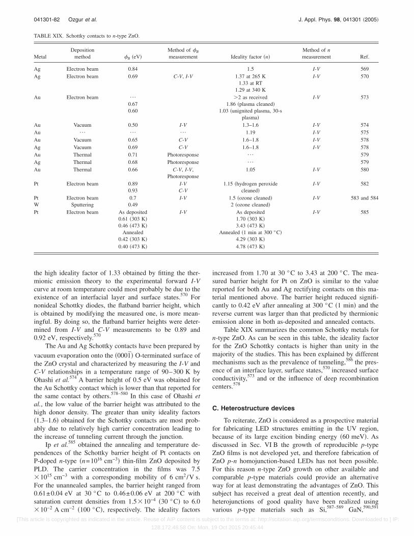
the high ideality factor of 1.33 obtained by fitting the ther-mionic emission theory to the experimental forward I-Vcurve at room temperature could most probably be due to theexistence of an interfacial layer and surface states.570 Fornonideal Schottky diodes, the flatband barrier height, whichis obtained by modifying the measured one, is more mean-ingful. By doing so, the flatband barrier heights were deter-mined from I-V and C-V measurements to be 0.89 and0.92 eV, respectively.570
The Au and Ag Schottky contacts have been prepared by
vacuum evaporation onto the �0001̄� O-terminated surface ofthe ZnO crystal and characterized by measuring the I-V andC-V relationships in a temperature range of 90–300 K byOhashi et al.574 A barrier height of 0.5 eV was obtained forthe Au Schottky contact which is lower than that reported forthe same contact by others.578–580 In this case of Ohashi etal., the low value of the barrier height was attributed to thehigh donor density. The greater than unity ideality factors�1.3–1.6� obtained for the Schottky contacts are most prob-ably due to relatively high carrier concentration leading tothe increase of tunneling current through the junction.
Ip et al.585 obtained the annealing and temperature de-pendences of the Schottky barrier height of Pt contacts onP-doped n-type �n=1016 cm−3� thin-film ZnO deposited byPLD. The carrier concentration in the films was 7.5�1015 cm−3 with a corresponding mobility of 6 cm2/V s.For the unannealed samples, the barrier height ranged from0.61±0.04 eV at 30 °C to 0.46±0.06 eV at 200 °C withsaturation current densities from 1.5�10−4 �30 °C� to 6.0�10−2 A cm−2 �100 °C�, respectively. The ideality factors
increased from 1.70 at 30 °C to 3.43 at 200 °C. The mea-sured barrier height for Pt on ZnO is similar to the valuereported for both Au and Ag rectifying contacts on this ma-terial mentioned above. The barrier height reduced signifi-cantly to 0.42 eV after annealing at 300 °C �1 min� and thereverse current was larger than that predicted by thermionicemission alone in both as-deposited and annealed contacts.
Table XIX summarizes the common Schottky metals forn-type ZnO. As can be seen in this table, the ideality factorfor the ZnO Schottky contacts is higher than unity in themajority of the studies. This has been explained by differentmechanisms such as the prevalence of tunneling,586 the pres-ence of an interface layer, surface states,570 increased surfaceconductivity,573 and or the influence of deep recombinationcenters.578
C. Heterostructure devices
To reiterate, ZnO is considered as a prospective materialfor fabricating LED structures emitting in the UV region,because of its large excition binding energy �60 meV�. Asdiscussed in Sec. VI B the growth of reproducible p-typeZnO films is not developed yet, and therefore fabrication ofZnO p-n homojunction-based LEDs has not been possible.For this reason n-type ZnO growth on other available andcomparable p-type materials could provide an alternativeway for at least demonstrating the advantages of ZnO. Thissubject has received a great deal of attention recently, andheterojunctions of good quality have been realized usingvarious p-type materials such as Si,587–589 GaN,590,591
TABLE XIX. Schottky contacts to n-type ZnO.
MetalDeposition
method �B �eV�Method of �B
measurement Ideality factor �n�Method of nmeasurement Ref.
Ag Electron beam 0.84 1.5 I-V 569Ag Electron beam 0.69 C-V, I-V 1.37 at 265 K
1.33 at RT1.29 at 340 K
I-V 570
Au Electron beam ¯
0.670.60
�2 as received1.86 �plasma cleaned�
1.03 �unignited plasma, 30-splasma�
I-V 573
Au Vacuum 0.50 I-V 1.3–1.6 I-V 574Au ¯ ¯ ¯ 1.19 I-V 575Au Vacuum 0.65 C-V 1.6–1.8 I-V 578Ag Vacuum 0.69 C-V 1.6–1.8 I-V 578Au Thermal 0.71 Photoresponse ¯ 579Ag Thermal 0.68 Photoresponse ¯ 579Au Thermal 0.66 C-V, I-V,
Photoresponse1.05 I-V 580
Pt Electron beam 0.890.93
I-VC-V
1.15 �hydrogen peroxidecleaned�
I-V 582
PtW
Electron beamSputtering
0.70.49
I-V 1.5 �ozone cleaned�2 �ozone cleaned�
I-V 583 and 584
Pt Electron beam As deposited0.61 �303 K�0.46 �473 K�
Annealed0.42 �303 K�
I-V As deposited1.70 �303 K�3.43 �473 K�
Annealed �1 min at 300 °C�4.29 �303 K�
I-V 585
0.40 �473 K� 4.78 �473 K�
041301-82 Ozgur et al. J. Appl. Phys. 98, 041301 �2005�
[This article is copyrighted as indicated in the article. Reuse of AIP content is subject to the terms at: http://scitation.aip.org/termsconditions. Downloaded to ] IP:
128.172.48.58 On: Mon, 19 Oct 2015 20:45:44
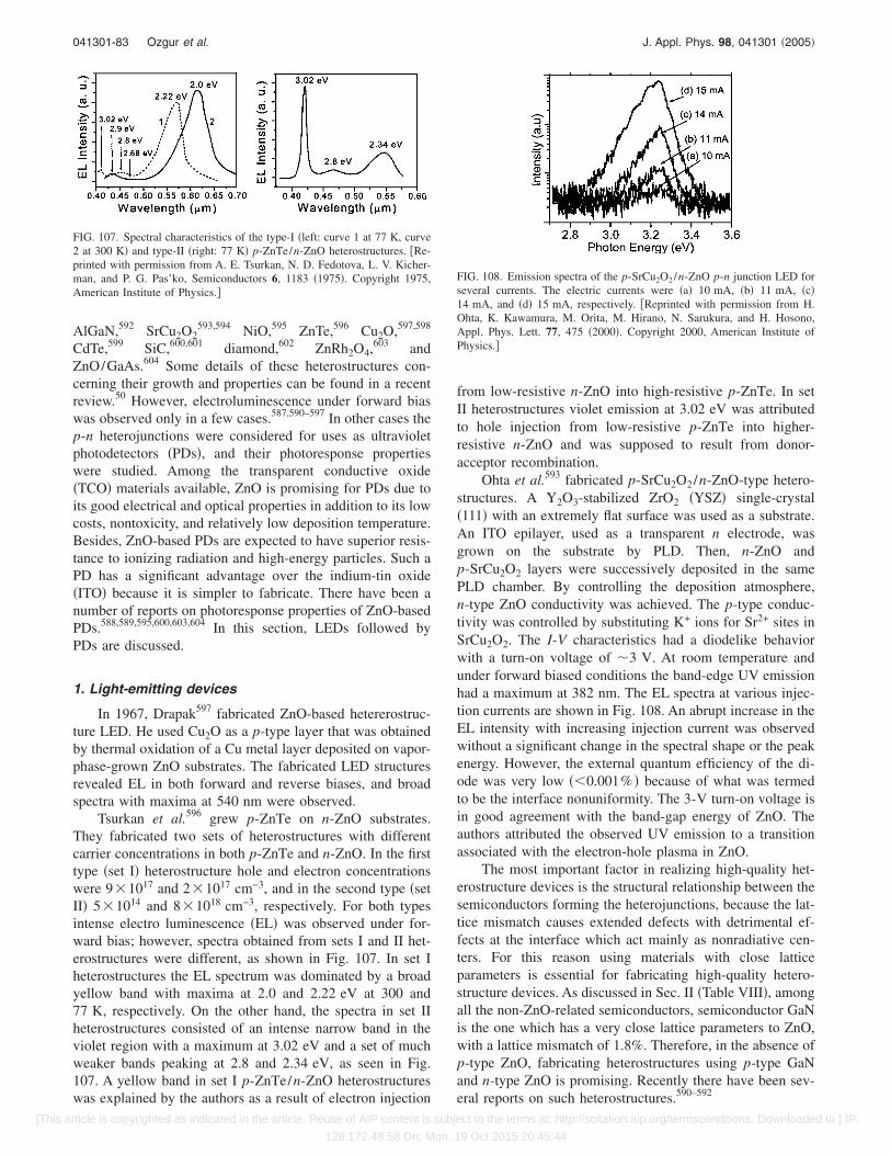
AlGaN,592 SrCu2O2593,594 NiO,595 ZnTe,596 Cu2O,597,598
CdTe,599 SiC,600,601 diamond,602 ZnRh2O4,603 andZnO/GaAs.604 Some details of these heterostructures con-cerning their growth and properties can be found in a recentreview.50 However, electroluminescence under forward biaswas observed only in a few cases.587,590–597 In other cases thep-n heterojunctions were considered for uses as ultravioletphotodetectors �PDs�, and their photoresponse propertieswere studied. Among the transparent conductive oxide�TCO� materials available, ZnO is promising for PDs due toits good electrical and optical properties in addition to its lowcosts, nontoxicity, and relatively low deposition temperature.Besides, ZnO-based PDs are expected to have superior resis-tance to ionizing radiation and high-energy particles. Such aPD has a significant advantage over the indium-tin oxide�ITO� because it is simpler to fabricate. There have been anumber of reports on photoresponse properties of ZnO-basedPDs.588,589,595,600,603,604 In this section, LEDs followed byPDs are discussed.
1. Light-emitting devices
In 1967, Drapak597 fabricated ZnO-based hetererostruc-ture LED. He used Cu2O as a p-type layer that was obtainedby thermal oxidation of a Cu metal layer deposited on vapor-phase-grown ZnO substrates. The fabricated LED structuresrevealed EL in both forward and reverse biases, and broadspectra with maxima at 540 nm were observed.
Tsurkan et al.596 grew p-ZnTe on n-ZnO substrates.They fabricated two sets of heterostructures with differentcarrier concentrations in both p-ZnTe and n-ZnO. In the firsttype �set I� heterostructure hole and electron concentrationswere 9�1017 and 2�1017 cm−3, and in the second type �setII� 5�1014 and 8�1018 cm−3, respectively. For both typesintense electro luminescence �EL� was observed under for-ward bias; however, spectra obtained from sets I and II het-erostructures were different, as shown in Fig. 107. In set Iheterostructures the EL spectrum was dominated by a broadyellow band with maxima at 2.0 and 2.22 eV at 300 and77 K, respectively. On the other hand, the spectra in set IIheterostructures consisted of an intense narrow band in theviolet region with a maximum at 3.02 eV and a set of muchweaker bands peaking at 2.8 and 2.34 eV, as seen in Fig.107. A yellow band in set I p-ZnTe/n-ZnO heterostructureswas explained by the authors as a result of electron injection
from low-resistive n-ZnO into high-resistive p-ZnTe. In setII heterostructures violet emission at 3.02 eV was attributedto hole injection from low-resistive p-ZnTe into higher-resistive n-ZnO and was supposed to result from donor-acceptor recombination.
Ohta et al.593 fabricated p-SrCu2O2/n-ZnO-type hetero-structures. A Y2O3-stabilized ZrO2 �YSZ� single-crystal�111� with an extremely flat surface was used as a substrate.An ITO epilayer, used as a transparent n electrode, wasgrown on the substrate by PLD. Then, n-ZnO andp-SrCu2O2 layers were successively deposited in the samePLD chamber. By controlling the deposition atmosphere,n-type ZnO conductivity was achieved. The p-type conduc-tivity was controlled by substituting K+ ions for Sr2+ sites inSrCu2O2. The I-V characteristics had a diodelike behaviorwith a turn-on voltage of �3 V. At room temperature andunder forward biased conditions the band-edge UV emissionhad a maximum at 382 nm. The EL spectra at various injec-tion currents are shown in Fig. 108. An abrupt increase in theEL intensity with increasing injection current was observedwithout a significant change in the spectral shape or the peakenergy. However, the external quantum efficiency of the di-ode was very low ��0.001% � because of what was termedto be the interface nonuniformity. The 3-V turn-on voltage isin good agreement with the band-gap energy of ZnO. Theauthors attributed the observed UV emission to a transitionassociated with the electron-hole plasma in ZnO.
The most important factor in realizing high-quality het-erostructure devices is the structural relationship between thesemiconductors forming the heterojunctions, because the lat-tice mismatch causes extended defects with detrimental ef-fects at the interface which act mainly as nonradiative cen-ters. For this reason using materials with close latticeparameters is essential for fabricating high-quality hetero-structure devices. As discussed in Sec. II �Table VIII�, amongall the non-ZnO-related semiconductors, semiconductor GaNis the one which has a very close lattice parameters to ZnO,with a lattice mismatch of 1.8%. Therefore, in the absence ofp-type ZnO, fabricating heterostructures using p-type GaNand n-type ZnO is promising. Recently there have been sev-eral reports on such heterostructures.590–592
FIG. 107. Spectral characteristics of the type-I �left: curve 1 at 77 K, curve2 at 300 K� and type-II �right: 77 K� p-ZnTe/n-ZnO heterostructures. �Re-printed with permission from A. E. Tsurkan, N. D. Fedotova, L. V. Kicher-man, and P. G. Pas’ko, Semiconductors 6, 1183 �1975�. Copyright 1975,American Institute of Physics.�
FIG. 108. Emission spectra of the p-SrCu2O2/n-ZnO p-n junction LED forseveral currents. The electric currents were �a� 10 mA, �b� 11 mA, �c�14 mA, and �d� 15 mA, respectively. �Reprinted with permission from H.Ohta, K. Kawamura, M. Orita, M. Hirano, N. Sarukura, and H. Hosono,Appl. Phys. Lett. 77, 475 �2000�. Copyright 2000, American Institute ofPhysics.�
041301-83 Ozgur et al. J. Appl. Phys. 98, 041301 �2005�
[This article is copyrighted as indicated in the article. Reuse of AIP content is subject to the terms at: http://scitation.aip.org/termsconditions. Downloaded to ] IP:
128.172.48.58 On: Mon, 19 Oct 2015 20:45:44

Alivov et al.590 have reported growth, processing, andfabrication of n-ZnO/ p-GaN heterojunction LED devices,where the 1-�m-thick CVD-grown n-ZnO �Ga-doped� andthe MBE-grown p-GaN �Mg-doped� layers had carrier con-centrations of 4.5�1018 and 3�1017 cm−3, respectively.Cathodoluminescence measurements have shown two sets ofpeaks appearing at 390 and 510 nm, and 383 and 430 nm forZnO and GaN, respectively. EL was observed under forwardbias and the spectrum consisted of a band with a maximumat 430 nm as depicted in Fig. 109, and it has been pointedout that EL emerges from p-GaN, where the radiative recom-bination occurs, since the probable band alignment favorselectron injection from the n-ZnO to the p-GaN.
To favor hole injection into ZnO thereby promote emis-sion in that material, Alivov et al.592 fabricated n-ZnO/p-Al0.12Ga0.88N heterojunction LEDs on 6H-SiC substrates, aschematic depiction of which is shown in Fig. 110. Diode-like, rectifying I-V characteristics, with a turn-on voltage of�3.2 V and a low reverse leakage current of �10−7 A wereobserved at room temperature. As shown in Fig. 111, anintense 389-nm UV emission, which was stable at tempera-tures up to 500 K, is observed when the diode is forwardbiased. It was also shown that this emission originated fromthe excitonic recombination within the ZnO layer. The en-ergy diagram for this heterostructure obtained from theAnderson model605 shows a higher barrier for electrons thanthat for holes �valence- and conduction-band offsets of 0.11
and 0.45 eV, respectively�. Therefore, hole injection fromwider-band-gap Al0.12Ga0.88N side �Eg�3.64 eV� into ZnOside �Eg�3.3 eV� of the heterojunction is much more likelyand is responsible for recombination emission in ZnO asopposed to the p-GaN/n-ZnO case where the electron injec-tion from ZnO to GaN with a concomitant emission in GaNdominated the spectrum. It should be pointed out, of course,that the Anderson model describes the band diagram for theideal case where there is no lattice mismatch between con-tacting materials and there are no imperfections at the inter-face; however, it allows us to sketch the most probable het-erojunction band alignment.
Similar results were obtained recently from n-Mg0.1
Zn0.9O/n-ZnO/ p-Al0.16Ga0.84N/ p-GaN triple heterostructureLEDs fabricated by Osinsky et al.606 The strong electrolumi-nescence at 390 nm, observed under forward bias, was alsoattributed to excitonic recombination in the ZnO layer. Theseresults show that p-AlGaN is a good candidate for fabricat-ing efficient heterostructure LEDs with ZnO active layers.
For potential ZnO-based laser diodes, lasing would oc-cur due to excitonic UV transitions and would therefore leadto much lower threshold currents compared to other materi-als. It is well known that employing a p-n-n �or n-p-p� -typedouble heterostructure �DH� �a quantum well straddled bylarger band-gap barrier layers� is a very effective means toachieving low threshold laser diodes owing to better carrierand optical confinement that provides higher internal quan-tum efficiencies, lower diffraction losses, superinjection, andweaker temperature dependence. The carrier confinement, re-sulting from the potential barriers at both sides of the hetero-junctions, increases the carrier density in the recombinationregion and practically eliminates the spread of the injectedcarriers beyond the active region. Consequently, growth ofZnO-based DH placing ZnO between wider-band-gap p- andn-type materials �for example, GaN, ZnMgO, and AlGaN�could pave the way for fabrication of laser diodes with ZnOas the active layer. Recently Alivov et al.607 demonstratedhigh-quality p-GaN/n-ZnO/n-GaN DH with good I-V andEL characteristics. A 0.7-�m-thick Mg-doped p-type GaNlayer was deposited first on a c-plane sapphire substrate byOMVPE. On this composite an unintentionally doped 0.4-�m-thick n-type ZnO layer was grown by plasma-assisted
FIG. 109. Electroluminescence spectrum of an n-ZnO/ p-GaN heterostruc-ture. �Reprinted with permission from Ya. I. Alivov, J. E. Van Nostrand, D.C. Look, M. V. Chukichev, and B. M. Ataev, Appl. Phys. Lett. 83, 2943�2003�. Copyright 2003, American Institute of Physics.�
FIG. 110. Schematic diagram of the n-ZnO/ p-Al0.12Ga0.88N heterojunctionLED structure �after Alivov et al. �Ref. 592��.
FIG. 111. Electroluminescence spectra of an n-ZnO/ p-Al0.12Ga0.88N hetero-structure light-emitting diode at 300 and 500 K. �Reprinted with permissionfrom Ya. I. Alivov, E. V. Kalinina. A. E. Cherenkov,D. C. Look, B. M.Ataev, A. K. Omaev, M. V. Chukichev, and D. M. Bagnall, Appl. Phys. Lett.83, 4719 �2003�. Copyright 2003, American Institute of Physics.�
041301-84 Ozgur et al. J. Appl. Phys. 98, 041301 �2005�
[This article is copyrighted as indicated in the article. Reuse of AIP content is subject to the terms at: http://scitation.aip.org/termsconditions. Downloaded to ] IP:
128.172.48.58 On: Mon, 19 Oct 2015 20:45:44

MBE at a substrate temperature of 600 °C. Finally, a 0.4-�m-thick n-GaN layer was grown at 550 °C on then-ZnO layer by plasma-assisted MBE. In Fig. 112 scanningelectron microscopy of this n-GaN/n-ZnO/ p-GaN doubleheterostructure is presented, indicating sharp interfaces to theextent discernable by scanning electron microscopy �SEM�.Fabricated diode structure exhibited rectifying diodelike be-havior with low leakage current of 4.4�10−7 A and a break-down voltage of 12 V. At room temperature EL was ob-served under forward bias, which blueshifted with increasingbias, as shown in Fig. 113. From a comparison of EL withthe PL spectra of n-ZnO and p-GaN it was concluded thatthe emission is primarily from the ZnO region of the DH.Since DH lasers are greatly dependent on the physical prop-erties of the well layer and its thickness which in this case isZnO, by modifying these parameters the quality of such DHcould be significantly improved.
2. Photodiodes
There have been many reports regarding the photore-sponse properties of the ZnO-based hetero-junctions.588,589,595,600,603,604 For example, Jeong et al.588 re-ported on the photoelectric properties of n-ZnO/p-Si photodiode �PD� which detect UV photons in the de-pleted n-ZnO and simultaneously detect visible photons inthe depleted p-Si by employing two related photoelectricmechanisms. The I-V measurements obtained while the pho-todiodes are exposed to radiation in a wavelength range of
310–650 nm showed a linear increase in photocurrent withreverse bias. In the visible range, the photocurrent rose rap-idly with bias but saturated beyond a critical voltage. Thediodes exhibited high responsivities of 0.5 and 0.3 A/W forUV �310-nm� and red �650-nm� photons, respectively, undera 30-V bias with a minimum near 380 nm which correspondsto the band gap of ZnO.
Transparent window p-NiO/n-ZnO PDs were heteroepi-taxially grown by Ohta et al.595 on a YSZ �111� substrate byPLD combined with a solid-phase-epitaxy technique. Thefabricated diodes exhibited clear rectifying I-V characteris-tics with an ideality factor of �2 and a forward turn-onvoltage of �1 V. Spectral responsivity measurements wereperformed via photoexcitation from the substrate side using amonochromated Xe lamp light under several reverse-biasconditions. A photoresponsivity as high as �0.3 A W−1 wasachieved at 26-V reverse bias under irradiation by 360-nmlight that corresponds to the ZnO energy gap.
Ohta et al.603 also reported on transparent p-n hetero-junctions composed of p-ZnRh2O4 and n-ZnO thin layersgrown by reactive solid-phase epitaxy technique �Fig. 114�.Polycrystalline ZnRh2O4 was deposited on a ZnO epitaxiallayer at room temperature. Thermal annealing of the bilayersample at 950 °C in air converted the polycrystallineZnRh2O4 layer to what was reported to be an epitaxialsingle-crystalline layer. The resultant p-n heterojunctions hadan abrupt interface and exhibited distinct rectifying I-V char-acteristics with a threshold voltage of �2 V that is in agree-ment with the band-gap energy of ZnRh2O4. The photovolt-age originating mainly from the n-ZnO layer was alsoobserved.
As discussed above, the critical factor influencing theproperties of heterostructures is the similarity of the latticeparameters. In this respect 6H-SiC seems to be a good can-didate since it has a relatively small lattice mismatch withZnO ��4%, Table VIII�, and p-6H-SiC substrates are com-mercially available. Alivov et al.600,601 fabricated n-ZnO/p-6H-SiC-type PDs growing 0.5-�m-thick n-ZnO layer onp-type 6H-SiC substrates at 600 °C by plasma-assisted MBEand demonstrated high-quality p-n heterojunctions. Ohmiccontacts to the 250-�m-diameter mesastructures were made
FIG. 112. Scanning electron microscope image of the grown n-GaN/n-ZnO/ p-GaN double heterostructure �after Alivov et al. �Ref. 607��.
FIG. 113. Electroluminescence spectra of the n-GaN/n-ZnO/ p-GaN doubleheterostructure diode at various forward biases �after Alivov et al. �Ref.607��.
FIG. 114. Spectral response of the p-ZnRh2O4/n-ZnO diode at severalreverse-bias voltages. The device structure is also shown in the inset. �Re-printed with permission from H. Ohta, M. Hirano, K. Nakahara, H. Maruta,T. Tanabe, M. Kamiya, T. Kamiya, and H. Hosono, Appl. Phys. Lett. 83,1029 �2003�. Copyright 2003, American Institute of Physics.�
041301-85 Ozgur et al. J. Appl. Phys. 98, 041301 �2005�
[This article is copyrighted as indicated in the article. Reuse of AIP content is subject to the terms at: http://scitation.aip.org/termsconditions. Downloaded to ] IP:
128.172.48.58 On: Mon, 19 Oct 2015 20:45:44
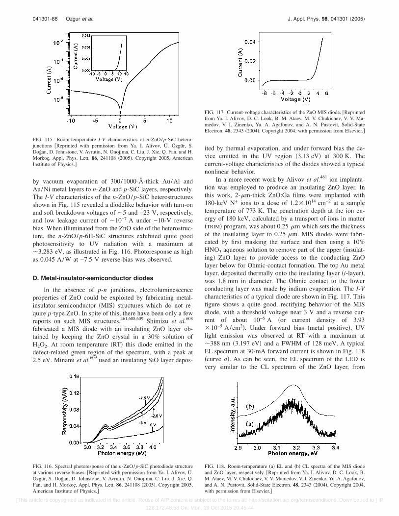
by vacuum evaporation of 300/1000-Å-thick Au/Al andAu/Ni metal layers to n-ZnO and p-SiC layers, respectively.The I-V characteristics of the n-ZnO/ p-SiC heterostructuresshown in Fig. 115 revealed a diodelike behavior with turn-onand soft breakdown voltages of �5 and −23 V, respectively,and low leakage current of �10−7 A under −10-V reversebias. When illuminated from the ZnO side of the heterostruc-ture, the n-ZnO/ p-6H-SiC structures exhibited quite goodphotosensitivity to UV radiation with a maximum at�3.283 eV, as illustrated in Fig. 116. Photoresponse as highas 0.045 A/W at −7.5-V reverse bias was observed.
D. Metal-insulator-semiconductor diodes
In the absence of p-n junctions, electroluminescenceproperties of ZnO could be exploited by fabricating metal-insulator-semiconductor �MIS� structures which do not re-quire p-type ZnO. In spite of this, there have been only a fewreports on such MIS structures.461,608,609 Shimizu et al.608
fabricated a MIS diode with an insulating ZnO layer ob-tained by keeping the ZnO crystal in a 30% solution ofH2O2. At room temperature �RT� this diode emitted in thedefect-related green region of the spectrum, with a peak at2.5 eV. Minami et al.609 used an insulating SiO layer depos-
ited by thermal evaporation, and under forward bias the de-vice emitted in the UV region �3.13 eV� at 300 K. Thecurrent-voltage characteristics of the diodes showed a typicalnonlinear behavior.
In a more recent work by Alivov et al.461 ion implanta-tion was employed to produce an insulating ZnO layer. Inthis work, 2-�m-thick ZnO:Ga films were implanted with180-keV N+ ions to a dose of 1.2�1014 cm−2 at a sampletemperature of 773 K. The penetration depth at the ion en-ergy of 180 keV, calculated by a transport of ions in matter�TRIM� program, was about 0.25 �m which sets the thicknessof the insulating layer to 0.25 �m. MIS diodes were fabri-cated by first masking the surface and then using a 10%HNO3 aqueous solution to remove part of the upper �insulat-ing� ZnO layer to provide access to the conducting ZnOlayer below for Ohmic-contact formation. The top Au metallayer, deposited thermally onto the insulating layer �i-layer�,was 1.8 mm in diameter. The Ohmic contact to the lowerconducting layer was made by indium evaporation. The I-Vcharacteristics of a typical diode are shown in Fig. 117. Thisfigure shows a quite good, rectifying behavior of the MISdiode, with a threshold voltage near 3 V and a reverse cur-rent of about 10−6 A �or current density of 3.93�10−5 A/cm2�. Under forward bias �metal positive�, UVlight emission was observed at RT with a maximum at�388 nm �3.197 eV� and a FWHM of 128 meV. A typicalEL spectrum at 30-mA forward current is shown in Fig. 118�curve a�. As can be seen, the EL spectrum of the LED isvery similar to the CL spectrum of the ZnO layer, from
FIG. 115. Room-temperature I-V characteristics of n-ZnO/ p-SiC hetero-junctions �Reprinted with permission from Ya. I. Alivov, Ü. Özgür, S.Doğan, D. Johnstone, V. Avrutin, N. Onojima, C. Liu, J. Xie, Q. Fan, and H.Morkoç, Appl. Phys. Lett. 86, 241108 �2005�. Copyright 2005, AmericanInstitute of Physics.�
FIG. 116. Spectral photoresponse of the n-ZnO/ p-SiC photodiode structureat various reverse biases. �Reprinted with permission from Ya. I. Alivov, Ü.Özgür, S. Doğan, D. Johnstone, V. Avrutin, N. Onojima, C. Liu, J. Xie, Q.Fan, and H. Morkoç, Appl. Phys. Lett. 86, 241108 �2005�. Copyright 2005,American Institute of Physics.�
FIG. 117. Current-voltage characteristics of the ZnO MIS diode. �Reprintedfrom Ya. I. Alivov, D. C. Look, B. M. Ataev, M. V. Chukichev, V. V. Ma-medov, V. I. Zinenko, Yu. A. Agafonov, and A. N. Pustovit, Solid-StateElectron. 48, 2343 �2004�, Copyright 2004, with permission from Elsevier.�
FIG. 118. Room-temperature �a� EL and �b� CL spectra of the MIS diodeand ZnO layer, respectively. �Reprinted from Ya. I. Alivov, D. C. Look, B.M. Ataev, M. V. Chukichev, V. V. Mamedov, V. I. Zinenko, Yu. A. Agafonov,and A. N. Pustovit, Solid-State Electron. 48, 2343 �2004�, Copyright 2004,with permission from Elsevier.�
041301-86 Ozgur et al. J. Appl. Phys. 98, 041301 �2005�
[This article is copyrighted as indicated in the article. Reuse of AIP content is subject to the terms at: http://scitation.aip.org/termsconditions. Downloaded to ] IP:
128.172.48.58 On: Mon, 19 Oct 2015 20:45:44

which it can be concluded that the radiation mechanisms inboth cases are similar, that is very probably excitonic in na-ture. No EL emission was observed under reverse-bias con-ditions for both MIS structure and that without an insulatinglayer. It is known that the properties of the MIS diodes de-pend strongly on the properties of the isolation layer—on itsthickness and electrical properties. Creating a MIS diode inthis manner, therefore, is of special interest since ion implan-tation is a very controllable technology and suitable for fab-rication of various microelectronics structures. Moreover, di-odes of this type are of interest not only in the design of lightemitters, but also in the development of transparent transis-tors.
E. Transparent thin-film transistors
There has been a great interest in transparent electronicslately,610 especially in conjunction with transparent thin-filmtransistors �TTFTs�, because it is expected that the character-istics of TTFT will not degrade on exposure to visible lightdue to the wide band gap of its active channel layer, whereasthe characteristics of amorphous or poly-Si TFT do degrade.Therefore, measures would not be required in this case toshield the active channel layer from visible light. ZnO forthis purpose is considered as one of the best candidates be-cause of properties such as high voltage, temperature, andradiation tolerance. Besides, high-quality crystalline ZnOfilms can be grown at relatively low deposition temperatureson various substrates including amorphous glasses. In thisvein, a number of reports are already available on ZnO-basedTTFT �Refs. 611–616� using various methods for ZnOgrowth.
The most important electrical parameters in quantifyingTFT performance are the drain-current on-to-off ratio andactive channel mobility. In terms of these parameters, thebest TTFT performance has been reported by Hoffman etal.613 Highly transparent ZnO-based TTFTs with opticaltransmittance �including substrate� of �75% for visible lighthave been fabricated by rf sputtering method. A typical sche-matic of TTFT structure reported is shown in Fig. 119. Aglass substrate was blanket coated with a 200-nm-thick layerof sputtered ITO and a 220-nm-thick layer of aluminum-titanium oxide �ATO� deposited by atomic layer deposition.ITO, a highly transparent and n-type conductor, served as theTTFT gate. The ATO layer acted as the gate insulator. TheZnO channel and ITO source/drain electrode films were de-posited via ion-beam sputtering in 1024 Torr of Ar/O2
�80% /20% �; the substrate was unheated during deposition.Shadow masks were used to pattern the ZnO channel andITO source/drain electrodes. The channel width and lengthwere 15 000 and 1500 �m, respectively, with a width-to-length ratio of 10:1, the source/drain contact dimensionswere 15 000�1500 �m2. After deposition of the ZnO layer,a rapid thermal anneal, typically at 600–800 °C in O2, wasemployed to increase the ZnO channel resistivity in order toimprove the electrical quality of the ATO/ZnO interface, andto enhance the crystallinity of the ZnO layer. Following thedeposition of the ITO source/drain electrodes, a 300 °Crapid thermal annealing in O2 was performed to improve thetransparency of the ITO layer. Figure 120 displays dc drain-current–drain-voltage �ID-VDS� curves for a TTFT. Current-voltage measurements indicate n-channel, enhancement-mode TFT operation with excellent drain-current saturationand a drain-current on-to-off ratio of �107. Typical TTFT dctransfer characteristics �log�ID�-VGS� and gate leakage cur-rent �log��IG��-VGS�, involving the drain current ID, gate cur-rent IG, and the gate voltage VGS, are presented in Fig. 120.These curves indicate a maximum drain-current on-to-off ra-tio of �107. In Ref. 614 channel mobility as high as25 cm2/V was also reported.
In another report, Carcia et al.616 fabricated ZnO thin-film transistors by rf magnetron sputtering on heavily dopedn-type Si substrates held near room temperature. In thisstructure, the substrate side was coated with a thermal oxidelayer of �100 nm thick. Ti–Au source and drain electrodes200 �m wide with a 20-�m gap �10-nm Ti followed by100-nm Au� were deposited and patterned directly on the
FIG. 119. The schematics of a typical TTFT structure. �Reprinted withpermission from R. L. Hoffman, B. J. Norris, and J. F. Wager, Appl. Phys.Lett. 82, 733 �2003�. Copyright 2003, American Institute of Physics.�
FIG. 120. Electrical characteristics of TTFT: �a� drain-current–drain-voltage�ID-VDS� characteristics; �b� transfer characteristics and gate leakage currentfor a TTFT with a width-to-length ratio of 10:1 for VDS=10 V. �Reprintedwith permission from R. L. Hoffman, B. J. Norris, and J. F. Wager, Appl.Phys. Lett. 82, 733 �2003�. Copyright 2003, American Institute of Physics.�
041301-87 Ozgur et al. J. Appl. Phys. 98, 041301 �2005�
[This article is copyrighted as indicated in the article. Reuse of AIP content is subject to the terms at: http://scitation.aip.org/termsconditions. Downloaded to ] IP:
128.172.48.58 On: Mon, 19 Oct 2015 20:45:44
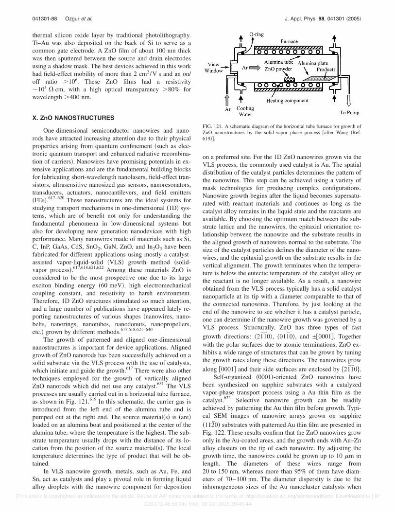
thermal silicon oxide layer by traditional photolithography.Ti–Au was also deposited on the back of Si to serve as acommon gate electrode. A ZnO film of about 100 nm thickwas then sputtered between the source and drain electrodesusing a shadow mask. The best devices achieved in this workhad field-effect mobility of more than 2 cm2/V s and an on/off ratio �106. These ZnO films had a resistivity�105 � cm, with a high optical transparency �80% forwavelength �400 nm.
X. ZnO NANOSTRUCTURES
One-dimensional semiconductor nanowires and nano-rods have attracted increasing attention due to their physicalproperties arising from quantum confinement �such as elec-tronic quantum transport and enhanced radiative recombina-tion of carriers�. Nanowires have promising potentials in ex-tensive applications and are the fundamental building blocksfor fabricating short-wavelength nanolasers, field-effect tran-sistors, ultrasensitive nanosized gas sensors, nanoresonators,transducers, actuators, nanocantilevers, and field emitters�FEs�.617–620 These nanostructures are the ideal systems forstudying transport mechanisms in one-dimensional �1D� sys-tems, which are of benefit not only for understanding thefundamental phenomena in low-dimensional systems butalso for developing new generation nanodevices with highperformance. Many nanowires made of materials such as Si,C, InP, GaAs, CdS, SnO2, GaN, ZnO, and In2O3 have beenfabricated for different applications using mostly a catalyst-assisted vapor-liquid-solid �VLS� growth method �solid-vapor process�.617,618,621,622 Among these materials ZnO isconsidered to be the most prospective one due to its largeexciton binding energy �60 meV�, high electromechanicalcoupling constant, and resistivity to harsh environment.Therefore, 1D ZnO structures stimulated so much attention,and a large number of publications have appeared lately re-porting nanostructures of various shapes �nanowires, nano-belts, nanorings, nanotubes, nanodonuts, nanopropellers,etc.� grown by different methods.617,618,621–640
The growth of patterned and aligned one-dimensionalnanostructures is important for device applications. Alignedgrowth of ZnO nanorods has been successfully achieved on asolid substrate via the VLS process with the use of catalysts,which initiate and guide the growth.617 There were also othertechniques employed for the growth of vertically alignedZnO nanorods which did not use any catalyst.631 The VLSprocesses are usually carried out in a horizontal tube furnace,as shown in Fig. 121.619 In this schematic, the carrier gas isintroduced from the left end of the alumina tube and ispumped out at the right end. The source material�s� is �are�loaded on an alumina boat and positioned at the center of thealumina tube, where the temperature is the highest. The sub-strate temperature usually drops with the distance of its lo-cation from the position of the source material�s�. The localtemperature determines the type of product that will be ob-tained.
In VLS nanowire growth, metals, such as Au, Fe, andSn, act as catalysts and play a pivotal role in forming liquidalloy droplets with the nanowire component for deposition
on a preferred site. For the 1D ZnO nanowires grown via theVLS process, the commonly used catalyst is Au. The spatialdistribution of the catalyst particles determines the pattern ofthe nanowires. This step can be achieved using a variety ofmask technologies for producing complex configurations.Nanowire growth begins after the liquid becomes supersatu-rated with reactant materials and continues as long as thecatalyst alloy remains in the liquid state and the reactants areavailable. By choosing the optimum match between the sub-strate lattice and the nanowires, the epitaxial orientation re-lationship between the nanowire and the substrate results inthe aligned growth of nanowires normal to the substrate. Thesize of the catalyst particles defines the diameter of the nano-wires, and the epitaxial growth on the substrate results in thevertical alignment. The growth terminates when the tempera-ture is below the eutectic temperature of the catalyst alloy orthe reactant is no longer available. As a result, a nanowireobtained from the VLS process typically has a solid catalystnanoparticle at its tip with a diameter comparable to that ofthe connected nanowires. Therefore, by just looking at theend of the nanowire to see whether it has a catalyst particle,one can determine if the nanowire growth was governed by aVLS process. Structurally, ZnO has three types of fast
growth directions: �21̄1̄0�, �011̄0�, and ±�0001�. Togetherwith the polar surfaces due to atomic terminations, ZnO ex-hibits a wide range of structures that can be grown by tuningthe growth rates along these directions. The nanowires grow
along �0001� and their side surfaces are enclosed by �21̄1̄0�.Self-organized �0001�-oriented ZnO nanowires have
been synthesized on sapphire substrates with a catalyzedvapor-phase transport process using a Au thin film as thecatalyst.622 Selective nanowire growth can be readilyachieved by patterning the Au thin film before growth. Typi-cal SEM images of nanowire arrays grown on sapphire
�112̄0� substrates with patterned Au thin film are presented inFig. 122. These results confirm that the ZnO nanowires growonly in the Au-coated areas, and the growth ends with Au–Znalloy clusters on the tip of each nanowire. By adjusting thegrowth time, the nanowires could be grown up to 10 �m inlength. The diameters of these wires range from20 to 150 nm, whereas more than 95% of them have diam-eters of 70–100 nm. The diameter dispersity is due to theinhomogeneous sizes of the Au nanocluster catalysts when
FIG. 121. A schematic diagram of the horizontal tube furnace for growth ofZnO nanostructures by the solid-vapor phase process �after Wang �Ref.619��.
041301-88 Ozgur et al. J. Appl. Phys. 98, 041301 �2005�
[This article is copyrighted as indicated in the article. Reuse of AIP content is subject to the terms at: http://scitation.aip.org/termsconditions. Downloaded to ] IP:
128.172.48.58 On: Mon, 19 Oct 2015 20:45:44

the substrate is annealed during the growth process. Haupt etal.639 were able to reduce the average diameter of the nano-wires below 30 nm using the same technique. The capabilityof patterned nanowire growth helps to fabricate nanoscalelight emitters in a controllable fashion.
Room-temperature PL spectra of ZnO nanowires showeda strong band-edge emission at �377 nm. In addition, a veryweak blue band �440–480 nm� and an almost negligiblegreen band �510–580 nm� were observed. These sampleswere explored for possible stimulated emission at room tem-perature by measuring the excitation density-dependentemission with excitation from the fourth harmonic of aNd:yttrium-aluminum-garnet �Nd:YAG� laser �266 nm, 3-nspulse width�. Light emission was collected in the directionnormal to the end surface plane �along the c axis� of thenanowires, and lasing was observed in the absence of anyfabricated mirrors with increasing pump power, as shown inFig. 123. At low excitation intensities, the spectrum consistsof a single broad spontaneous emission peak �Fig. 123� witha full width at half maximum of 17 nm. When the excitationintensity exceeds a threshold of 40 kW/cm2 sharp peaksemerged in the emission spectra. The linewidths of thesepeaks are 0.3 nm, which are 50 times smaller than the line-width of the spontaneous emission peak. Above the thresh-old, the integrated emission intensity increases rapidly withthe pump power indicating that stimulated emission takesplace in these nanowires. The observed single or multiplesharp peaks between 370 and 400 nm represent different las-ing modes. The lasing action in these nanowire arrays with-out any fabricated mirrors is possible if one considers thesesingle-crystalline, well-faceted nanowires as natural reso-nance cavities. One end of the nanowire is the epitaxial in-terface between the sapphire and ZnO, whereas the other endis the sharp �0001� plane of the ZnO nanocrystals. Both endsserved as good laser cavity mirrors, since the refractive indexfor ZnO is more than that for sapphire and air �2.45, 1.8, and1, respectively�. This natural cavity or waveguide formationin nanowires provides a simple approach to forming a nano-wire laser cavity without cleavage and etching.
Park et al.631 reported on the metal-organic vapor-phaseepitaxial �MOVPE� growth of ZnO nanorods. The nanorods
were grown on Al2O3 �0001� substrates at 400 °C withoutemploying any metal catalysts usually needed in other meth-ods �Fig. 124�. The mean diameter of nanorods obtained byMOVPE was as small as 25 nm, smaller than the typicaldiameters of 50–100 nm for those prepared by other depo-sition methods.622 Furthermore, the ZnO nanorods were wellaligned vertically, showing uniformity in their diameters,lengths, and densities as revealed from electron microscopy.The results of -2 scan, -rocking curve, and �-scan mea-surements on the nanorods are presented in Fig. 125. Onlythe �002� and �004� diffraction peaks are visible in the XRD-2 scans shown in Fig. 125�a�, and a small full width athalf maximum �FWHM� value of 0.6° was obtained from theXRD -rocking curve measurements �Fig. 125�b��. Further-more, Fig. 125�c� shows a sixfold rotational symmetry in theazimuthal scan. These results clearly indicate that the ZnOnanorods were epitaxially grown with homogeneous in-planealignment as well as c-axis orientation. The PL spectra of thenanorods showed strong and narrow excitonic emission witha dominant peak at 3.29 eV and an extremely weak deep-level emission at 2.5 eV, indicating the high optical qualityof the nanorods.
Li et al.633 prepared ZnO nanoneedles on a silicon waferthrough chemical-vapor deposition. The diameters of theneedle tips were in the range of 20–50 nm. High-resolutiontransmission electron microscopy revealed that the nanon-eedles were single crystals growing along the �0001� direc-tion and exhibiting multiple tip surface perturbations, andwere just 1–3 nm in dimension. Field-emission measure-
FIG. 122. Scanning electron microscope images of ZnO nanowire arraysgrown on sapphire substrates ��a�–�e��. A top view of the well-faceted hex-agonal nanowire tips is shown in �e�. �f� High-resolution TEM image of anindividual ZnO nanowire showing its �0001� growth direction. �Reprintedwith permission from M. H. Huang, S. Mao, H. Feick, H. Yan, Y. Wu, H.Kind, E. Weber, R. Russo, and P. Yang, Science 292, 1897 �2001�. Copyright2001 AAAS.�
FIG. 123. Emission spectra from nanowire arrays below �line a� and above�line b and inset� the lasing threshold. The pump power levels for thesespectra are 20, 100, and 150 kW/cm2, respectively. The spectra are offsetfor easy comparison. �Reprinted with permission from M. H. Huang, S.Mao, H. Feick, H. Yan, Y. Wu, H. Kind, E. Weber, R. Russo, and P. Yang,Science 292, 1897 �2001�. Copyright 2001 AAAS.�
041301-89 Ozgur et al. J. Appl. Phys. 98, 041301 �2005�
[This article is copyrighted as indicated in the article. Reuse of AIP content is subject to the terms at: http://scitation.aip.org/termsconditions. Downloaded to ] IP:
128.172.48.58 On: Mon, 19 Oct 2015 20:45:44

ments on the prepared nanostructures showed fairly lowturn-on and threshold fields of 2.5 and 4.0 V/mm, respec-tively. The nanosize perturbations on the nanoneedle tips areassumed to cause such excellent field-emission performance.The high emission current density, high stability, and lowturn-on field make the ZnO nanoneedle arrays one of thepromising candidates for high brightness field-emission elec-tron sources and flat-panel displays.
Könenkamp et al.641 fabricated vertical nanowire LEDsusing ZnO nanowires grown by electrodeposition from aque-ous solutions on fluorine-doped SnO2-coated glass sub-strates. Since during electrodeposition, the growth of ZnOcolumns �100–200 nm in diameter and 2 �m in length� pro-ceeded under electron injection from the underlying SnO2
layer, a good electronic contact between SnO2 and ZnO wasassumed. The space between the nanowires was filled withpolystyrene and a 0.5–1.5-�m coating of poly�3,4-ethylene-dioxythiophene��PEDOT�/poly�styrenesulfonate� was ap-plied to establish a p-type contact to the nanowire tips. Fi-nally, a 100-nm-thick Au layer was deposited by vacuumevaporation to provide a Schottky-barrier-type contact forhole injection. EL was observed from the device at a thresh-old of 10 V with a current density of �100 mA/cm2 at thenanowire tips. Similar to PL from uncoated nanowires, ELshowed a broad defect-related emission centered at 620 nm.The more than an order of magnitude weaker UV band-edge
emission was observed as a shoulder at 384 nm. Even thoughfurther improvements are needed on the device to enhancethe UV emission, the ZnO nanowire LEDs showed a stableoperation for �1 h.
Nanobelts are nanowires that have a well-defined geo-metrical shape and side surfaces. Nanobelts of ZnO are usu-ally grown by sublimation of ZnO powder without acatalyst.642 Due to differences in surface energies among
�0001�, �011̄0�, and �21̄1̄0�, freestanding nanobelts andnanowires of ZnO are usually dominated by the lower-
energy, nonpolar surfaces such as �011̄0� and �21̄1̄0�. When
there is no doping, the nanobelt grows along �011̄0�, with top
and bottom flat surfaces ±�21̄1̄0� and side surfaces ±�0001�.Pan et al.642 were able to grow nanobelts with each nanobelthaving a uniform width along its entire length and the typical
FIG. 124. FE-SEM �a� plan-view and �b� tilted images of ZnO nanorodswith a mean diameter of 25 nm and �c� tilted and �d� cross-sectional imagesof ZnO nanorods with a mean diameter of 70 nm. In �c�, hexagon-shapedpyramids with flat terraces and steps are seen at the ends of the nanorods.�Reprinted with permission from W. I. Park, D. H. Kim, S.-W. Jung, andG.-C. Yi, Appl. Phys. Lett. 80, 4232 �2002�. Copyright 2002, AmericanInstitute of Physics.�
FIG. 125. XRD �a� -2 scan, �b� rocking curve, and �c� azimuthal ��� scanmeasurement results of ZnO nanorods. From the XRD -2 scan data, onlytwo peaks are shown at 34.32° and 72.59° which correspond to ZnO �002�and �004� peaks, respectively. The rocking curve also shows a FWHM valueof 0.6°. A sixfold symmetry in the �-scan data is also observed, indicatingin-plane alignment of the nanorods. �Reprinted with permission from W. I.Park, D. H. Kim, S.-W. Jung, and G.-C. Yi, Appl. Phys. Lett. 80, 4232�2002�. Copyright 2002, American Institute of Physics.�
041301-90 Ozgur et al. J. Appl. Phys. 98, 041301 �2005�
[This article is copyrighted as indicated in the article. Reuse of AIP content is subject to the terms at: http://scitation.aip.org/termsconditions. Downloaded to ] IP:
128.172.48.58 On: Mon, 19 Oct 2015 20:45:44
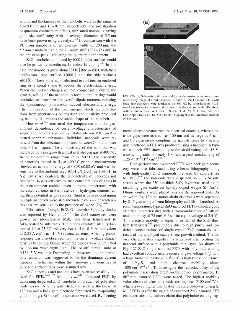
widths and thicknesses of the nanobelts were in the range of50–300 nm and 10–30 nm, respectively. For investigationof quantum confinement effects, ultrasmall nanobelts havinggood size uniformity with an average diameter of 5.5 nmhave been grown using a catalyst.643 In comparison with thePL from nanobelts of an average width of 200 nm, the5.5-nm nanobelts exhibited a 14-nm shift �387–373 nm� inthe emission peak, indicating the quantum confinement.
ZnO nanobelts dominated by �0001� polar surfaces couldalso be grown by introducing In and/or Li doping.644 In this
case, the nanobelts grow along �21̄1̄0� �the a-axis�, with theirtop/bottom large surface ±�0001� and the side surfaces
±�011̄0�. These polar nanobelts tend to roll into an enclosedring or a spiral shape to reduce the electrostatic energy.When the surface charges are not compensated during thegrowth, rolling of the nanobelt to form a circular ring wouldminimize or neutralize the overall dipole moment, reducingthe spontaneous polarization-induced electrostatic energy.The minimization of the total energy, which has contribu-tions from spontaneous polarization and elasticity producedby bending, determines the stable shape of the nanobelt.
Heo et al.645 measured the temperature and the gas-ambient dependence of current-voltage characteristics ofsingle ZnO nanorods grown by catalyst-driven MBE on Au-coated sapphire substrates. Individual nanorods were re-moved from the substrate and placed between Ohmic-contactpads 3.7 �m apart. The conductivity of the nanorods wasincreased by a postgrowth anneal in hydrogen gas at 400 °C.In the temperature range from 25 to 150 °C, the resistivityof nanorods treated in H2 at 400 °C prior to measurementshowed an activation energy of 0.089±0.02 eV and was in-sensitive to the ambient used �C2H4,N2O,O2 or 10% H2 inN2�. By sharp contrast, the conductivity of nanorods nottreated in H2 was sensitive to trace concentrations of gases inthe measurement ambient even at room temperature, withincreased currents in the presence of hydrogen, demonstrat-ing their potential as gas sensors. Similar devices containingmultiple nanorods were also shown to have I–V characteris-tics that are sensitive to the presence of ozone �O3�.646
Fabrication of single Pt/ZnO nanowire Schottky diodeswas reported by Heo et al.647 The ZnO nanowires weregrown by site-selective MBE and then transferred toSiO2-coated Si substrates. The diodes exhibited ideality fac-tors of 1.1 at 25 °C and very low �1.5�10−10 A, equivalentto 2.35 A cm−2, at −10 V� reverse currents. A strong photo-response was also observed, with the current-voltage charac-teristics becoming Ohmic when the diodes were illuminatedby 366-nm wavelength light. The on-off current ratio at0.15/−5 V was �6. Depending on these results, the thermi-onic emission was suggested to be the dominant currenttransport mechanism within the nanowire and densities ofbulk and surface traps were assumed low.
ZnO nanorods and nanobelts have been successfully uti-lized for FETs.648–652 Arnold et al.648 fabricated FETs bydepositing dispersed ZnO nanobelts on predefined gold elec-trode arrays. A SiO2 gate dielectric with a thickness of120 nm and a back gate electrode fabricated by evaporatinggold on the p+ Si side of the substrate were used. By forming
metal electrode/nanostructure electrical contacts, where elec-trode gaps were as small as 100 nm and as large as 6 �m,and by capacitively coupling the nanostructure to a nearbygate electrode, a FET was produced using a nanobelt. A typi-cal nanobelt FET showed a gate threshold voltage of −15 V,a switching ratio of nearly 100, and a peak conductivity of1.25�10−3 �−1 cm−1.648
High-performance n-channel FETs with back gate geom-etry were also fabricated using e-beam lithography alongwith high-quality ZnO nanorods prepared by catalyst-freeMOVPE.649 The nanorods were dispersed on SiO2/Si sub-strates where the 250-nm-thick SiO2 layer was used as aninsulating gate oxide on heavily doped n-type Si. Au/TiOhmic contacts were placed only on the nanorod ends. Asshown in Fig. 126 the source-drain electrodes were separatedby 2–5 �m using e-beam lithography and lift-off method. Atroom temperature, typical ZnO nanorod FETs exhibited goodelectrical characteristics with a transconductance of 140 nSand a mobility of 75 cm2 V−1 s−1 �at a gate voltage of 2.4 V�.This electron mobility is higher than that of the ZnO thin-film transistors,653 presumably due to high purity and lowdefect concentrations of single-crystal ZnO nanorods as aresult of the employed catalyst-free growth method. The de-vice characteristics significantly improved after coating thenanorod surface with a polyimide thin layer. As shown inFig. 127 ZnO single nanorod FETs with polyimide coatinghad excellent conductance response to gate voltage �Vg� witha large turn-on/off ratio of 104–105, a high transconductanceof 1.9 �S, and high electron mobility above1000 cm2 V−1 s−1. To investigate the reproducibility of thepolyimide passivation effect on the device performance, 13different nanorod FETs were tested. The highest mobilityvalue observed after polyimide coating was 3100 cm2/V s,which is even higher than that of the state-of-the-art planar SiMOSFETs. As for the origin of enhanced ZnO nanorod FETcharacteristics, the authors claim that polyimide coating sup-
FIG. 126. �a� Schematic side view and �b� field-emission scanning electronmicroscopy image of a ZnO nanorod FET device. ZnO nanorod FETs withback gate geometry were fabricated on SiO2/Si by deposition of Au/Timetal electrodes for source-drain contacts on the nanorod ends. �Reprintedwith permission from W. I. Park, J. S. Kim, G.-C. Yi, M. H. Bae, and H.-J.Lee, Appl. Phys. Lett. 85, 5052 �2004�. Copyright 2004, American Instituteof Physics.�
041301-91 Ozgur et al. J. Appl. Phys. 98, 041301 �2005�
[This article is copyrighted as indicated in the article. Reuse of AIP content is subject to the terms at: http://scitation.aip.org/termsconditions. Downloaded to ] IP:
128.172.48.58 On: Mon, 19 Oct 2015 20:45:44
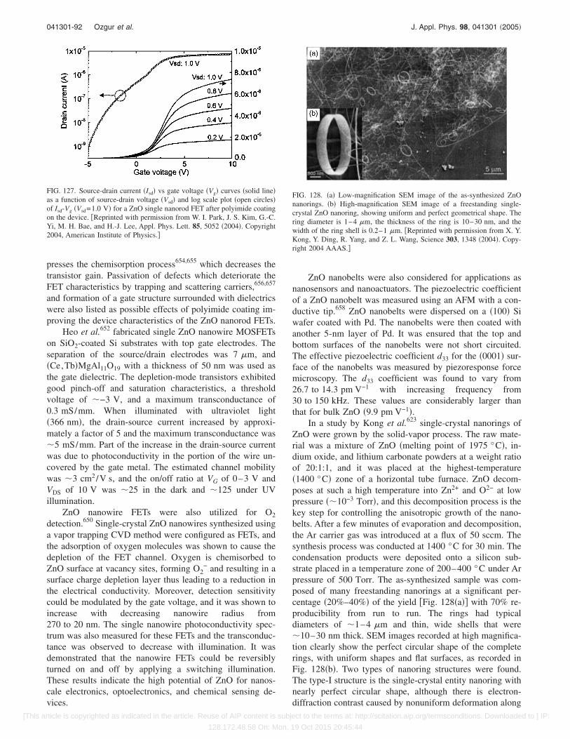
presses the chemisorption process654,655 which decreases thetransistor gain. Passivation of defects which deteriorate theFET characteristics by trapping and scattering carriers,656,657
and formation of a gate structure surrounded with dielectricswere also listed as possible effects of polyimide coating im-proving the device characteristics of the ZnO nanorod FETs.
Heo et al.652 fabricated single ZnO nanowire MOSFETson SiO2-coated Si substrates with top gate electrodes. Theseparation of the source/drain electrodes was 7 �m, and�Ce,Tb�MgAl11O19 with a thickness of 50 nm was used asthe gate dielectric. The depletion-mode transistors exhibitedgood pinch-off and saturation characteristics, a thresholdvoltage of �−3 V, and a maximum transconductance of0.3 mS/mm. When illuminated with ultraviolet light�366 nm�, the drain-source current increased by approxi-mately a factor of 5 and the maximum transconductance was�5 mS/mm. Part of the increase in the drain-source currentwas due to photoconductivity in the portion of the wire un-covered by the gate metal. The estimated channel mobilitywas �3 cm2/V s, and the on/off ratio at VG of 0–3 V andVDS of 10 V was �25 in the dark and �125 under UVillumination.
ZnO nanowire FETs were also utilized for O2
detection.650 Single-crystal ZnO nanowires synthesized usinga vapor trapping CVD method were configured as FETs, andthe adsorption of oxygen molecules was shown to cause thedepletion of the FET channel. Oxygen is chemisorbed toZnO surface at vacancy sites, forming O2
− and resulting in asurface charge depletion layer thus leading to a reduction inthe electrical conductivity. Moreover, detection sensitivitycould be modulated by the gate voltage, and it was shown toincrease with decreasing nanowire radius from270 to 20 nm. The single nanowire photoconductivity spec-trum was also measured for these FETs and the transconduc-tance was observed to decrease with illumination. It wasdemonstrated that the nanowire FETs could be reversiblyturned on and off by applying a switching illumination.These results indicate the high potential of ZnO for nanos-cale electronics, optoelectronics, and chemical sensing de-vices.
ZnO nanobelts were also considered for applications asnanosensors and nanoactuators. The piezoelectric coefficientof a ZnO nanobelt was measured using an AFM with a con-ductive tip.658 ZnO nanobelts were dispersed on a �100� Siwafer coated with Pd. The nanobelts were then coated withanother 5-nm layer of Pd. It was ensured that the top andbottom surfaces of the nanobelts were not short circuited.The effective piezoelectric coefficient d33 for the �0001� sur-face of the nanobelts was measured by piezoresponse forcemicroscopy. The d33 coefficient was found to vary from26.7 to 14.3 pm V−1 with increasing frequency from30 to 150 kHz. These values are considerably larger thanthat for bulk ZnO �9.9 pm V−1�.
In a study by Kong et al.623 single-crystal nanorings ofZnO were grown by the solid-vapor process. The raw mate-rial was a mixture of ZnO �melting point of 1975 °C�, in-dium oxide, and lithium carbonate powders at a weight ratioof 20:1:1, and it was placed at the highest-temperature�1400 °C� zone of a horizontal tube furnace. ZnO decom-poses at such a high temperature into Zn2+ and O2− at lowpressure ��10−3 Torr�, and this decomposition process is thekey step for controlling the anisotropic growth of the nano-belts. After a few minutes of evaporation and decomposition,the Ar carrier gas was introduced at a flux of 50 sccm. Thesynthesis process was conducted at 1400 °C for 30 min. Thecondensation products were deposited onto a silicon sub-strate placed in a temperature zone of 200–400 °C under Arpressure of 500 Torr. The as-synthesized sample was com-posed of many freestanding nanorings at a significant per-centage �20%–40%� of the yield �Fig. 128�a�� with 70% re-producibility from run to run. The rings had typicaldiameters of �1–4 �m and thin, wide shells that were�10–30 nm thick. SEM images recorded at high magnifica-tion clearly show the perfect circular shape of the completerings, with uniform shapes and flat surfaces, as recorded inFig. 128�b�. Two types of nanoring structures were found.The type-I structure is the single-crystal entity nanoring withnearly perfect circular shape, although there is electron-diffraction contrast caused by nonuniform deformation along
FIG. 127. Source-drain current �Isd� vs gate voltage �Vg� curves �solid line�as a function of source-drain voltage �Vsd� and log scale plot �open circles�of Isd-Vg �Vsd=1.0 V� for a ZnO single nanorod FET after polyimide coatingon the device. �Reprinted with permission from W. I. Park, J. S. Kim, G.-C.Yi, M. H. Bae, and H.-J. Lee, Appl. Phys. Lett. 85, 5052 �2004�. Copyright2004, American Institute of Physics.�
FIG. 128. �a� Low-magnification SEM image of the as-synthesized ZnOnanorings. �b� High-magnification SEM image of a freestanding single-crystal ZnO nanoring, showing uniform and perfect geometrical shape. Thering diameter is 1–4 �m, the thickness of the ring is 10–30 nm, and thewidth of the ring shell is 0.2–1 �m. �Reprinted with permission from X. Y.Kong, Y. Ding, R. Yang, and Z. L. Wang, Science 303, 1348 �2004�. Copy-right 2004 AAAS.�
041301-92 Ozgur et al. J. Appl. Phys. 98, 041301 �2005�
[This article is copyrighted as indicated in the article. Reuse of AIP content is subject to the terms at: http://scitation.aip.org/termsconditions. Downloaded to ] IP:
128.172.48.58 On: Mon, 19 Oct 2015 20:45:44

the circumference. The type-II structure nanoring is a singlecrystal, which again implies that the nanoring shell is a uni-formly deformed, single-crystal ribbon around the circumfer-ence.
Wang et al.637 reported that the Zn-terminated ZnO�0001� polar surface is chemically active and the oxygenterminated �0001� polar surface is inert during the growth ofnanocantilever arrays. It should be pointed out that the�0001� surface is the Zn-polar surface which upon exposure
to O could be O terminated. On the other hand, the �0001̄�surface is the O-polar surface. Caution must be exercised toavoid any confusion. Those authors grew relatively long andwide “comblike” nanocantilever arrays from the �0001�-Znsurface �Fig. 129� by a self-catalyzed process due to the en-richment of Zn at the growth front. The chemically inactive�0001�-O surface did not initiate any growth. The �0001�-Znsurface tended to have tiny Zn clusters at the growth front, asevidenced by the high-resolution TEM image. The Zn clus-ters as well as the local enrichment in Zn at the growth fronttend to initiate the growth of ZnO analogous to the vapor-liquid-solid growth process. Therefore, the self-catalyzed ef-fect of the Zn clusters resulted in a fast growth of the nan-otips. The �0001�-O terminated surface, however, is likely tobe inert and may not exhibit an effective self-catalyzed ef-fect; thus, the surface may not initiate the growth of nano-cantilevers. By changing the growth kinetics so that there isno growth on the �0001�-O terminated surface, a comblikestructure with long teeth only on one side has been grown, asdepicted in Fig. 129, with the top/bottom surfaces being
±�011̄0� and the side surfaces ±�21̄1̄0�. It is possible that achange in the growth condition results in the disappearanceof the �0111� type of facets; thus, the chemically inert �0001�surface does not initiate any teeth growth. The nanofingersshown in Fig. 129 could serve as nanocantilever arrays.
Combining microelectromechanical system �MEMS�technology with self-assembled nanobelts cost effective can-tilevers with much heightened sensitivity may be producedfor a range of devices and applications such as force, pres-sure, mass, thermal, biological, and chemical sensors. Semi-conducting nanobelts are ideal candidates for cantilever ap-
plications, since they are structurally defect-free singlecrystals and provide a significant improvement in the canti-lever sensitivity due to their reduced dimensions. IndividualZnO nanobelts could be aligned on Si chips to have a rangeof lengths and therefore different resonance frequencies.619
Zhang et al.659 reported on the formation of ZnO tubesby MOCVD at temperatures of 350–450 °C. The tubes ob-tained were grown epitaxially on sapphire �0001� substrateswith both the ZnO c axis and the growth direction beingparallel to the substrate normal. All of the tubes had hexago-nal cross sections and the same in-plane orientation. Thecharacteristics of the tubes were found to depend strongly onboth the growth temperature and reactor pressure. Figure 130shows SEM images of the tubes formed at 400 °C underdifferent reactor pressures. Figure 130�a� indicates that all ofthe tubes have hexagonal shapes and all the hexagons havethe same in-plane orientation. Figures 130�b�–130�d� showthe SEM images taken with an inclination angle of the tubesobtained at 0.3, 0.6, and 1.0 Torr, respectively. The densityof the hexagonal ZnO tubes decreased from 4 to 0.6 �m−2
with increasing pressure from 0.3 to 3 Torr. The well-defined hexagonal shape is an indication of epitaxial growthand consequently single-crystal nature of the tubes. TheXRD studies �rocking curve, -2 scan, and �-scan measure-ments� of the samples showed that the tubes were wellaligned both in the growth plane �in-plane� and along thegrowth direction �out-of-plane�. The growth temperature alsogreatly influenced the tube formation. In the temperaturerange of 350–450 °C, the density of the tubes increasedfrom 0.04 to 1 �m−2 and the outer sizes of the tubes de-creased from 1.0 to 0.4 �m with increasing temperature.
FIG. 129. Transmission electron microscopy image of a double-sided combstructure, showing the distinct arrays of nanotips and nanofingers on the twosides. The inset is the corresponding electron-diffraction pattern and theenlargements of the two selected areas, as indicated. �Reprinted with per-mission from Z. L. Wang, X. Y. Kong, and J. M. Zuo, Phys. Rev. Lett. 91,185502 �2003�. Copyright 2003 by the American Physical Society.�
FIG. 130. SEM images of ZnO tubes formed at 400 °C under differentreactor pressures. �a� Top image of the tubes obtained at 0.3 Torr. ��b�–�d��SEM images taken with an inclination angle of the tubes obtained at 0.3,0.6, and 1.0 Torr, respectively. �Reprinted with permission from B. P.Zhang, N. T. Binh, K. Wakatsuki, Y. Segawa, Y. Yamada, N. Usami, M.Kawasaki, and H. Koinuma, Appl. Phys. Lett. 84, 4098 �2004�. Copyright2004, American Institute of Physics.�
041301-93 Ozgur et al. J. Appl. Phys. 98, 041301 �2005�
[This article is copyrighted as indicated in the article. Reuse of AIP content is subject to the terms at: http://scitation.aip.org/termsconditions. Downloaded to ] IP:
128.172.48.58 On: Mon, 19 Oct 2015 20:45:44

However, no tubes were obtained at 500 °C. Therefore, thetube density can be modified by changing either the growthtemperature or the reactor pressure, and the tube size can betuned with the growth temperature.
As another example of various types of nanostructures,polar-surface-dominated ZnO nanopropeller arrays were syn-thesized using a two-step high-temperature solid-vapor depo-sition process by Gao and Wang.634 The first step involvesthe growth of the nanopropeller axis which is a straightnanowire along the c axis and enclosed by �2110� surfaces.In the second step, the sixfold symmetric nanoblades areformed along the crystallographic equivalent a axes ��2110��perpendicular to the nanowire, and the array is formed byepitaxial growth of nanoblades on the nanowire. The growthof the nanopropeller arrays on polycrystalline Al2O3 sub-strates was conducted at 600–700 °C for 60 min �step I� andthen at 800–900 °C for 30 min �step II� under pressure of200 mbars. Figure 131�a� shows a top view of the well-aligned ZnO nanopropeller arrays on a polycrystalline Al2O3
substrate grown in a relatively high temperature zone��680 °C, step I�. Each nanopropeller array column consistsof six arrays of triangular-shaped blades of 4–5 �m inlength and propeller arrays with a diameter of �10 �m. Thecolumns of the nanopropellers maintain their sixfold arraysof parallel nanoribbon blades around the central nanowire, asseen in Fig. 131�b�. The morphology and shape of the nano-propellers depended on the local temperature, surface diffu-sion rate, and availability of Zn–O vapor. In a lower-temperature region, due to a relatively slower surfacediffusion and the decrease in supply of the vapor as moresource material is being consumed, a triangular-shaped struc-ture was formed. In the medium-temperature region, a faster
diffusion of the Zn–O vapor and higher surface mobility leadto the formation of uniform and longer nanoblades.
There have also been reports on the growth of ZnO tet-rapod structures.635,636 In Ref. 636 such structures were pre-pared either from oxidation of Zn in air or by heating amixture of ZnO and graphite �1:1� at 1100 °C in a tubefurnace. Djurišić et al.636 also fabricated ZnO samples byheating a mixture of ZnO, GeO2, and graphite at 1100 °Cand studied the morphology of the fabricated structures as afunction of GeO2 percentage up to 10%. Figure 132 showsthe representative SEM images of the obtained ZnO struc-tures. Similar tetrapod structures are obtained for both start-ing materials �Zn and ZnO:C�. When GeO2 is added to thestarting material �ZnO:C�, multipod structures started toform, as illustrated in Fig. 132�c�. With increasing GeO2 con-
FIG. 131. SEM images of bunches of ZnO nanopropeller arrays rooted atAl2O3 substrate grown at various temperatures: �a� a single column of theas-synthesized ZnO nanopropeller arrays; �b� front view of a column of ZnOnanopropeller arrays with nanowires at the central axis, which was collectedfrom a lower-temperature zone ��620 °C�; �c� a column of ZnO nanopro-peller arrays with uniform nanoribbon shape and smoother surface, whichwas collected from a medium-temperature zone ��650 °C�; and �d� a col-umn of ZnO nanopropeller arrays with long nanoribbons, which was col-lected from a higher-temperature zone ��680 °C�. �Reprinted with permis-sion from P. X. Gao, and Z. L. Wang, Appl. Phys. Lett. 84, 2883 �2004�.Copyright 2004, American Institute of Physics.�
FIG. 132. Representative SEM images of ZnO nanostructures: �a� ZnOprepared from Zn, �b� ZnO prepared from ZnO:C, and �c� ZnO preparedfrom ZnO:C:GeO2. �Reprinted with permission from A. B. Djurišić, Y. H.Leung, W. C. H. Choy, K. W. Cheah, and W. K. Chan, Appl. Phys. Lett. 84,2635 �2004�. Copyright 2004, American Institute of Physics.�
041301-94 Ozgur et al. J. Appl. Phys. 98, 041301 �2005�
[This article is copyrighted as indicated in the article. Reuse of AIP content is subject to the terms at: http://scitation.aip.org/termsconditions. Downloaded to ] IP:
128.172.48.58 On: Mon, 19 Oct 2015 20:45:44
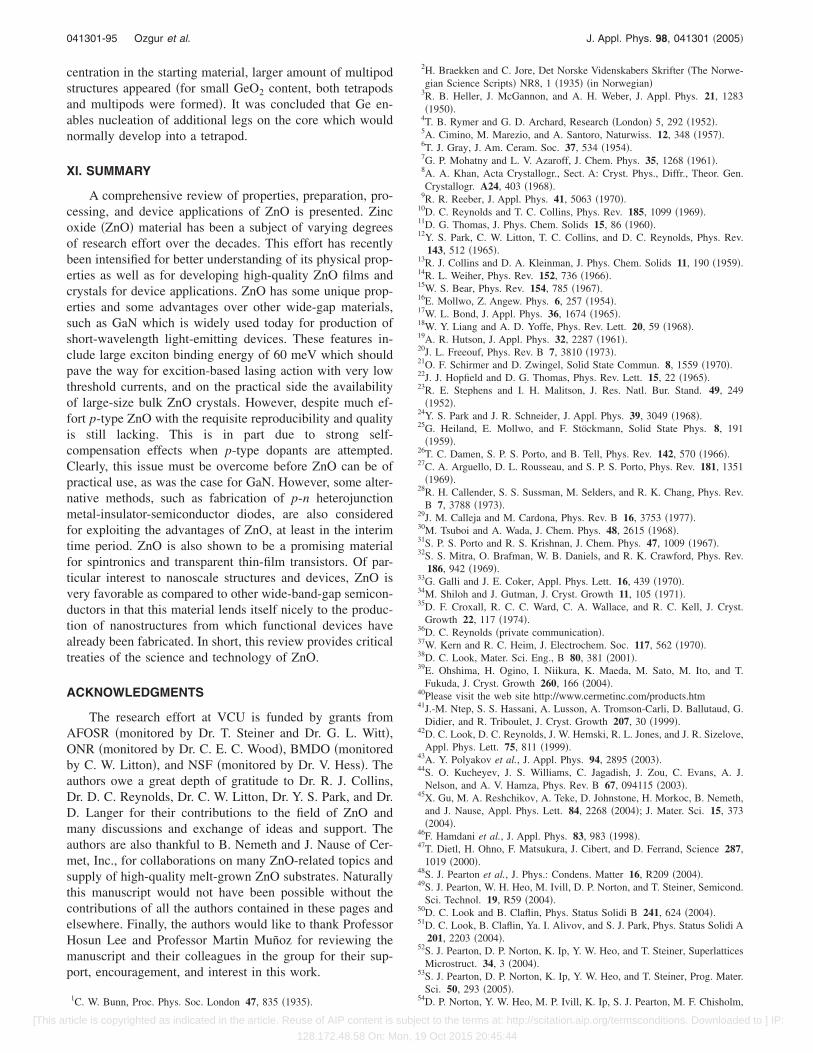
centration in the starting material, larger amount of multipodstructures appeared �for small GeO2 content, both tetrapodsand multipods were formed�. It was concluded that Ge en-ables nucleation of additional legs on the core which wouldnormally develop into a tetrapod.
XI. SUMMARY
A comprehensive review of properties, preparation, pro-cessing, and device applications of ZnO is presented. Zincoxide �ZnO� material has been a subject of varying degreesof research effort over the decades. This effort has recentlybeen intensified for better understanding of its physical prop-erties as well as for developing high-quality ZnO films andcrystals for device applications. ZnO has some unique prop-erties and some advantages over other wide-gap materials,such as GaN which is widely used today for production ofshort-wavelength light-emitting devices. These features in-clude large exciton binding energy of 60 meV which shouldpave the way for excition-based lasing action with very lowthreshold currents, and on the practical side the availabilityof large-size bulk ZnO crystals. However, despite much ef-fort p-type ZnO with the requisite reproducibility and qualityis still lacking. This is in part due to strong self-compensation effects when p-type dopants are attempted.Clearly, this issue must be overcome before ZnO can be ofpractical use, as was the case for GaN. However, some alter-native methods, such as fabrication of p-n heterojunctionmetal-insulator-semiconductor diodes, are also consideredfor exploiting the advantages of ZnO, at least in the interimtime period. ZnO is also shown to be a promising materialfor spintronics and transparent thin-film transistors. Of par-ticular interest to nanoscale structures and devices, ZnO isvery favorable as compared to other wide-band-gap semicon-ductors in that this material lends itself nicely to the produc-tion of nanostructures from which functional devices havealready been fabricated. In short, this review provides criticaltreaties of the science and technology of ZnO.
ACKNOWLEDGMENTS
The research effort at VCU is funded by grants fromAFOSR �monitored by Dr. T. Steiner and Dr. G. L. Witt�,ONR �monitored by Dr. C. E. C. Wood�, BMDO �monitoredby C. W. Litton�, and NSF �monitored by Dr. V. Hess�. Theauthors owe a great depth of gratitude to Dr. R. J. Collins,Dr. D. C. Reynolds, Dr. C. W. Litton, Dr. Y. S. Park, and Dr.D. Langer for their contributions to the field of ZnO andmany discussions and exchange of ideas and support. Theauthors are also thankful to B. Nemeth and J. Nause of Cer-met, Inc., for collaborations on many ZnO-related topics andsupply of high-quality melt-grown ZnO substrates. Naturallythis manuscript would not have been possible without thecontributions of all the authors contained in these pages andelsewhere. Finally, the authors would like to thank ProfessorHosun Lee and Professor Martin Muñoz for reviewing themanuscript and their colleagues in the group for their sup-port, encouragement, and interest in this work.
1C. W. Bunn, Proc. Phys. Soc. London 47, 835 �1935�.
2H. Braekken and C. Jore, Det Norske Videnskabers Skrifter �The Norwe-gian Science Scripts� NR8, 1 �1935� �in Norwegian�
3R. B. Heller, J. McGannon, and A. H. Weber, J. Appl. Phys. 21, 1283�1950�.
4T. B. Rymer and G. D. Archard, Research �London� 5, 292 �1952�.5A. Cimino, M. Marezio, and A. Santoro, Naturwiss. 12, 348 �1957�.6T. J. Gray, J. Am. Ceram. Soc. 37, 534 �1954�.7G. P. Mohatny and L. V. Azaroff, J. Chem. Phys. 35, 1268 �1961�.8A. A. Khan, Acta Crystallogr., Sect. A: Cryst. Phys., Diffr., Theor. Gen.Crystallogr. A24, 403 �1968�.
9R. R. Reeber, J. Appl. Phys. 41, 5063 �1970�.10D. C. Reynolds and T. C. Collins, Phys. Rev. 185, 1099 �1969�.11D. G. Thomas, J. Phys. Chem. Solids 15, 86 �1960�.12Y. S. Park, C. W. Litton, T. C. Collins, and D. C. Reynolds, Phys. Rev.
143, 512 �1965�.13R. J. Collins and D. A. Kleinman, J. Phys. Chem. Solids 11, 190 �1959�.14R. L. Weiher, Phys. Rev. 152, 736 �1966�.15W. S. Bear, Phys. Rev. 154, 785 �1967�.16E. Mollwo, Z. Angew. Phys. 6, 257 �1954�.17W. L. Bond, J. Appl. Phys. 36, 1674 �1965�.18W. Y. Liang and A. D. Yoffe, Phys. Rev. Lett. 20, 59 �1968�.19A. R. Hutson, J. Appl. Phys. 32, 2287 �1961�.20J. L. Freeouf, Phys. Rev. B 7, 3810 �1973�.21O. F. Schirmer and D. Zwingel, Solid State Commun. 8, 1559 �1970�.22J. J. Hopfield and D. G. Thomas, Phys. Rev. Lett. 15, 22 �1965�.23R. E. Stephens and I. H. Malitson, J. Res. Natl. Bur. Stand. 49, 249
�1952�.24Y. S. Park and J. R. Schneider, J. Appl. Phys. 39, 3049 �1968�.25G. Heiland, E. Mollwo, and F. Stöckmann, Solid State Phys. 8, 191
�1959�.26T. C. Damen, S. P. S. Porto, and B. Tell, Phys. Rev. 142, 570 �1966�.27C. A. Arguello, D. L. Rousseau, and S. P. S. Porto, Phys. Rev. 181, 1351
�1969�.28R. H. Callender, S. S. Sussman, M. Selders, and R. K. Chang, Phys. Rev.
B 7, 3788 �1973�.29J. M. Calleja and M. Cardona, Phys. Rev. B 16, 3753 �1977�.30M. Tsuboi and A. Wada, J. Chem. Phys. 48, 2615 �1968�.31S. P. S. Porto and R. S. Krishnan, J. Chem. Phys. 47, 1009 �1967�.32S. S. Mitra, O. Brafman, W. B. Daniels, and R. K. Crawford, Phys. Rev.
186, 942 �1969�.33G. Galli and J. E. Coker, Appl. Phys. Lett. 16, 439 �1970�.34M. Shiloh and J. Gutman, J. Cryst. Growth 11, 105 �1971�.35D. F. Croxall, R. C. C. Ward, C. A. Wallace, and R. C. Kell, J. Cryst.
Growth 22, 117 �1974�.36D. C. Reynolds �private communication�.37W. Kern and R. C. Heim, J. Electrochem. Soc. 117, 562 �1970�.38D. C. Look, Mater. Sci. Eng., B 80, 381 �2001�.39E. Ohshima, H. Ogino, I. Niikura, K. Maeda, M. Sato, M. Ito, and T.
Fukuda, J. Cryst. Growth 260, 166 �2004�.40Please visit the web site http://www.cermetinc.com/products.htm41J.-M. Ntep, S. S. Hassani, A. Lusson, A. Tromson-Carli, D. Ballutaud, G.
Didier, and R. Triboulet, J. Cryst. Growth 207, 30 �1999�.42D. C. Look, D. C. Reynolds, J. W. Hemski, R. L. Jones, and J. R. Sizelove,
Appl. Phys. Lett. 75, 811 �1999�.43A. Y. Polyakov et al., J. Appl. Phys. 94, 2895 �2003�.44S. O. Kucheyev, J. S. Williams, C. Jagadish, J. Zou, C. Evans, A. J.
Nelson, and A. V. Hamza, Phys. Rev. B 67, 094115 �2003�.45X. Gu, M. A. Reshchikov, A. Teke, D. Johnstone, H. Morkoc, B. Nemeth,
and J. Nause, Appl. Phys. Lett. 84, 2268 �2004�; J. Mater. Sci. 15, 373�2004�.
46F. Hamdani et al., J. Appl. Phys. 83, 983 �1998�.47T. Dietl, H. Ohno, F. Matsukura, J. Cibert, and D. Ferrand, Science 287,
1019 �2000�.48S. J. Pearton et al., J. Phys.: Condens. Matter 16, R209 �2004�.49S. J. Pearton, W. H. Heo, M. Ivill, D. P. Norton, and T. Steiner, Semicond.
Sci. Technol. 19, R59 �2004�.50D. C. Look and B. Claflin, Phys. Status Solidi B 241, 624 �2004�.51D. C. Look, B. Claflin, Ya. I. Alivov, and S. J. Park, Phys. Status Solidi A
201, 2203 �2004�.52S. J. Pearton, D. P. Norton, K. Ip, Y. W. Heo, and T. Steiner, Superlattices
Microstruct. 34, 3 �2004�.53S. J. Pearton, D. P. Norton, K. Ip, Y. W. Heo, and T. Steiner, Prog. Mater.
Sci. 50, 293 �2005�.54D. P. Norton, Y. W. Heo, M. P. Ivill, K. Ip, S. J. Pearton, M. F. Chisholm,
041301-95 Ozgur et al. J. Appl. Phys. 98, 041301 �2005�
[This article is copyrighted as indicated in the article. Reuse of AIP content is subject to the terms at: http://scitation.aip.org/termsconditions. Downloaded to ] IP:
128.172.48.58 On: Mon, 19 Oct 2015 20:45:44

and T. Steiner, Mater. Today 7, 34 �2004�.55V. A. Nikitenko, J. Appl. Spectrosc. 52, 367 �1992�.56J. E. Jaffe and A. C. Hess, Phys. Rev. B 48, 7903 �1993�.57J. E. Jaffe, J. A. Snyder, Z. Lin, and A. C. Hess, Phys. Rev. B 62, 1660
�2000�.58CRC Handbook of Chemistry and Physics, 58th ed. �CRC, Boca Raton,
1977�.59E. Kisi and M. M. Elcombe, Acta Crystallogr., Sect. C: Cryst. Struct.
Commun. C45, 1867 �1989�.60C. H. Bates, W. B. White, and R. Roy, Science 137, 993 �1962�.61L. Gerward and J. S. Olsen, J. Synchrotron Radiat. 2, 233 �1995�.62J. M. Recio, M. A. Blanco, V. Luaña, R. Pandey, L. Gerward, and J. Staun
Olsen, Phys. Rev. B 58, 8949 �1998�.63J. C. Jamieson, Phys. Earth Planet. Inter. 3, 201 �1970�.64S. Desgreniers, Phys. Rev. B 58, 14102 �1998�.65H. Karzel et al., Phys. Rev. B 53, 11425 �1996�.66R. Ahuja, L. Fast, O. Eriksson, J. M. Wills, and B. Johansson, J. Appl.
Phys. 83, 8065 �1998�.67J. M. Recio, R. Pandey, and V. Luana, Phys. Rev. B 47, 3401 �1993�.68M. Wilson and P. A. Madden, Mol. Phys. 90, 75 �1997�.69L.-G. Liu and W. A. Bassett, Elements, Oxides, and Silicates: High-
Pressure Phases with Implications for the Earth’s Interior �Oxford Uni-versity, New York, 1986�.
70A. Zaoui and W. Sekkal, Phys. Rev. B 66, 174106-1 �2002�.71T. Kogure and Y. Bando, J. Electron Microsc. 47, 7903 �1993�.72A. B. M. A. Ashrafi, A. Ueta, A. Avramescu, H. Kumano, I. Suemune,
Y.-W. Ok, and T.-Y. Seong, Appl. Phys. Lett. 76, 550 �2000�.73S.-K. Kim, S.-Y. Jeong, and C.-R. Cho, Appl. Phys. Lett. 82, 562 �2003�.74W. L. Bond, Acta Crystallogr. 13, 814 �1960�.75F. J. Himpsel, Adv. Phys. 32, 1 �1983�.76U. Rössler, Phys. Rev. 184, 733 �1969�.77D. W. Langer and C. J. Vesely, Phys. Rev. B2, 4885 �1970�.78R. A. Powell, W. E. Spicer, and J. C. McMenamin, Phys. Rev. Lett. 27, 97
�1971�.79R. A. Powell, W. E. Spicer, and J. C. McMenamin, Phys. Rev. B 6, 3056
�1972�.80L. Ley, R. A. Pollak, F. R. McFeely, S. P. Kowalezyk, and D. A. Shirley,
Phys. Rev. B 9, 600 �1974�.81C. J. Vesely, R. L. Hengehold, and D. W. Langer, Phys. Rev. B 5, 2296
�1972�.82S. Bloom and I. Ortenburger, Phys. Status Solidi B 58, 561 �1973�.83J. R. Chelikowsky, Solid State Commun. 22, 351 �1977�.84I. Ivanov and J. Pollmann, Phys. Rev. B 24, 7275 �1981�.85D. H. Lee and J. D. Joannopoulos, Phys. Rev. B 24, 6899 �1981�.86P. Schröer, P. Krüger, and J. Pollmann, Phys. Rev. B 47, 6971 �1993�.87S. Massidda, R. Resta, M. Posternak, and A. Baldereschi, Phys. Rev. B
52, R16977 �1995�.88P. Schröer, P. Krüger, and J. Pollmann, Phys. Rev. B 49, 17092 �1994�.89D. Vogel, P. Krüger, and J. Pollmann, Phys. Rev. B 52, R14316 �1995�.90R. T. Girard, O. Tjernberg, G. Chiaia, S. Söderholm, U. O. Karlsson, C.
Wigren, H. Nylèn, and I. Lindau, Surf. Sci. 373, 409 �1997�.91C. B. Duke, A. R. Lubinsky, S. C. Chang, B. W. Lee, and P. Mark, Phys.
Rev. B 15, 4865 �1977�.92C. B. Duke, R. J. Meyer, A. Paton, and P. Mark, Phys. Rev. B 18, 4225
�1978�.93Y. R. Wang and C. B. Duke, Surf. Sci. 192, 309 �1987�.94W. Göpel, J. Pollmann, I. Ivanov, and B. Reihl, Phys. Rev. B 26, 3144
�1982�.95G. Zwicker and K. Jacobi, Solid State Commun. 54, 701 �1985�.96K. Ozawa, K. Sawada, Y. Shirotori, K. Edamoto, and M. Nakatake, Phys.
Rev. B 68, 125417 �2003�.97S. H. Wei and A. Zounger, Phys. Rev. B 37, 8958 �1988�.98J. L. Martins, N. Troullier, and S. H. Wei, Phys. Rev. B 43, 2213 �1991�.99Y.-N. Xu and W. Y. Ching, Phys. Rev. B 48, 4335 �1993�.100O. Zakharov, A. Rubio, X. Blasé, M. L. Cohen, and S. G. Louie, Phys.
Rev. B 50, 10780 �1994�.101N. A. Hill and U. Waghmare, Phys. Rev. B 62, 8802 �2000�.102J. E. Jaffe, R. Pandey, and A. B. Kunz, Phys. Rev. B 43, 14030 �1991�.103E. Hückel, Z. Phys. 70, 204 �1931�.104A. Polian, M. Grimsditch, and I. Grzegory, J. Appl. Phys. 79, 3343
�1996�.105T. B. Bateman, J. Appl. Phys. 35, 3309 �1962�.106F. D. Murnaghan, Proc. Natl. Acad. Sci. U.S.A. 30, 244 �1944�.107A. Dal Corso, M. Posternak, R. Resta, and A. Baldereschi, Phys. Rev. B
50, 10715 �1994�.108J. F. Nye, Physical Properties of Crystals �Clarendon, Oxford, 1975�.109F. Bernardini, V. Fiorentini, and D. Vanderbilt, Phys. Rev. B 56, R10024
�1997�.110 H. Morkoç, Nitride Semiconductors and Devices �Springer, Berlin, 1999�.111 F. Decremps, J. Zhang, B. Li, and R. C. Liebermann, Phys. Rev. B 63,
224105 �2001�; F. Decremps, J. Pellicer-Porres, A. Marco Saitta, J.-C.Chervin, and A. Polian, Phys. Rev. B 65, 092101 �2002�.
112 N. Soga and O. L. Anderson, J. Appl. Phys. 38, 2985 �1967�.113 S. O. Kucheyev, J. E. Bradby, J. S. Williams, C. Jagadish, and M. V.
Swain, Appl. Phys. Lett. 80, 956 �2002�; S. O. Kucheyev, J. E. Bradby,J. S. Williams, C. Jagadish, M. Toth, M. R. Phillips, and M. V. Swain,Appl. Phys. Lett. 77, 3373 �2000�.
114 J. C. Phillips, Bonds and Bands in Semiconductors �Academic, NewYork, 1973�.
115 M. A. Stroscio and M. Dutta, Phonons in Nanostructures �CambridgeUniversity Press, Cambridge, 2001�.
116 B. H. Bairamov, A. Heinrich, G. Irmer, V. V. Toporov, and E. Ziegler,Phys. Status Solidi B 119, 227 �1983�.
117 Y. F. Lu, H. Q. Ni, and Z. M. Ren, J. Appl. Phys. 88, 498 �2000�.118 N. Ashkenov et al., J. Appl. Phys. 93, 126 �2003�.119 M. Rajalakshmi, A. K. Arora, B. S. Bendre, and S. Mahamuni, J. Appl.
Phys. 87, 2445 �2000�.120S. Minomura, High Pressure in Science and Technology, Proceedings of
the Ninth AIRAPT International High Pressure Conference on High Pres-sure in Science and Technology, edited by C. Homan, R. K. MacCrane,and E. Whalley�North-Holland, New York, 1984�, p. 277.
121S. Limpijumnong and W. R. L. Lambrecht, Phys. Rev. Lett. 86, 91�2001�; J. Serrano, A. Rubio, E. Hernández, A. Muñoz, and A. Mujica,Phys. Rev. B 62, 16612 �2000�.
122A. Kaschner et al., Appl. Phys. Lett. 80, 1909 �2002�.123C. Bundesmann, N. Ashkenov, M. Schubert, D. Spemann, T. Butz, E. M.
Kaidashev, M. Lorenz, and M. Grundmann, Appl. Phys. Lett. 83, 1974�2003�.
124C. G. Van de Walle, Phys. Rev. Lett. 85, 1012 �2000�.125M. D. McCluskey, S. J. Jokela, K. K. Zhuravlev, P. J. Simpson, and K. G.
Lynn, Appl. Phys. Lett. 81, 3807 �2002�; E. V. Lavrov, J. Weber, F.Börrnert, C. G. Van de Walle, and R. Helbig, Phys. Rev. B 66, 165205�2002�.
126E. V. Lavrov, Physica B 340–342, 195 �2003�.127E. V. Lavrov, J. Weber, F. Börrnert, C. G. Van de Walle, and R. Helbig,
Phys. Rev. B 66, 165205 �2002�.128M. D. McCluskey, S. J. Jokela, K. K. Zhuravlev, P. J. Simpson, and K. G.
Lynn, Appl. Phys. Lett. 81, 3807 �2002�.129S. J. Jokela, M. D. McCluskey, and K. G. Lynn, Physica B 340–342, 221
�2003�.130N. H. Nickel and K. Fleischer, Phys. Rev. Lett. 90, 197402 �2003�.131J. A. Wolk, J. W. Ager III, K. J. Duxstad, E. E. Haller, N. R. Taskar, D.
R. Dorman, and D. J. Olego, Appl. Phys. Lett. 63, 2756 �1993�.132H. Ibach, Phys. Status Solidi 33, 257 �1969�.133M.-Y. Han and J.-H. Jou, Thin Solid Films 260, 58 �1995�; F. Z.
Aoumeur, Kh. Benkabou, and B. Belgoumène, Physica B 337, 292�2003�.
134C. M. Bhandari and D. M. Rowe, Thermal Conduction in Semiconductors�Wiley, New York, 1988�.
135C. Kittel, Introduction to Solid State Physics, 6th ed. �Wiley, New York,1986�, p. 150.
136D. I. Florescu, V. M. Asnin, F. H. Pollak, R. J. Molnar, and C. E. C.Wood, J. Appl. Phys. 88, 3295 �2000�.
137D. I. Florescu, L. G. Mourokh, F. H. Pollak, D. C. Look, G. Cantwell, andX. Li, J. Appl. Phys. 91, 890 �2002�.
138F. H. Pollak, Ü. Özgür, S. Doğan, X. Gu, S.-J. Cho, H. Morkoç, and J.Nause �unpublished�.
139T. Olorunyolemi, A. Birnboim, Y. Carmel, O. C. Wilson, Jr., and I. K.Lloyd, J. Am. Ceram. Soc. 85, 1249 �2002�.
140T. Tsubota, M. Ohtaki, K. Eguchi, and H. Arai, J. Mater. Chem. 7, 85�1997�.
141M. Ohtaki, T. Tsubota, K. Eguchi, and H. Arai, J. Appl. Phys. 79, 1816�1996�.
142S. Katsuyama, Y. Takagi, M. Ito, K. Majima, H. Nagai, H. Sakai, K.Yoshimura, and K. Kosuge, J. Appl. Phys. 92, 1391 �2002�.
143T. Tsubota, M. Ohtaki, K. Eguchi, and H. Arai, J. Mater. Chem. 8, 409�1998�.
144K. F. Cai, E. Müller, C. Drašar, and A. Mrotzek, Mater. Sci. Eng., B 104,
041301-96 Ozgur et al. J. Appl. Phys. 98, 041301 �2005�
[This article is copyrighted as indicated in the article. Reuse of AIP content is subject to the terms at: http://scitation.aip.org/termsconditions. Downloaded to ] IP:
128.172.48.58 On: Mon, 19 Oct 2015 20:45:44

45 �2003�.145W. N. Lawless and T. K. Gupta, J. Appl. Phys. 60, 607 �1986�.146J. D. Albrecht, P. P. Ruden, S. Limpijumnong, W. R. L. Lambrecht, and
K. F. Brennan, J. Appl. Phys. 86, 6864 �1991�;D. C. Look, J. W. Hemsky,and J. R. Sizelove, Phys. Rev. Lett. 82, 2552 �1999�;D. C. Look, D. C.Reynolds, J. R. Sizelove, R. L. Jones, C. W. Litton, G. Cantwell, and W.C. Harsch, Solid State Commun. 105, 399 �1998�.
147D. S. Ginley and C. Bright, Mater. Res. Bull. 25, 15 �2000�; E. M.Kaidashev et al., Appl. Phys. Lett. 82, 3901 �2003�.
148H. Kato, M. Sano, K. Miyamoto, and T. Yao, Jpn. J. Appl. Phys., Part 142, 2241 �2003�;K. Iwata, P. Fons, S. Niki, A. Yamada, K. Matsubara, K.Nakahara, and H. Takasu, Phys. Status Solidi A 180, 287 �2000�;K.Miyamoto, M. Sano, H. Kato, and T. Yao, Jpn. J. Appl. Phys., Part 2 41,L1203 �2002�;J. Cryst. Growth 265, 34 �2004�;T. Edahiro, N. Fujimura,and T. Ito, J. Appl. Phys. 93, 7673 �2003�.
149T. Yamamoto, T. Shiosaki, and A. Kawabata, J. Appl. Phys. 51, 3113�1980�.
150T. Mitsuyu, S. Ono, and K. Wasa, J. Appl. Phys. 51, 2464 �1980�.151A. Hachigo, H. Nakahata, K. Higaki, S. Fujii, and S. Shikata, Appl. Phys.
Lett. 65, 2556 �1994�.152J. G. E. Gardeniers, Z. M. Rittersma, and G. J. Burger, J. Appl. Phys. 83,
7844 �1998�.153S. K. Tiku, C. K. Lau, and K. M. Lakin, Appl. Phys. Lett. 36, 318 �1980�.154M. Kasuga and M. Mochizuki, J. Cryst. Growth 54, 185 �1981�.155V. Srikant, V. Sergo, and D. R. Clarke, Appl. Phys. Lett. 16, 439 �1995�.156K.-K. Kim, J.-H. Song, H.-J. Jung, W.-K. Choi, S.-J. Park, and J.-H.
Song, J. Appl. Phys. 87, 3573 �2000�; K.-K. Kim, J.-H. Song, H.-J. Jung,W.-K. Choi, S.-J. Park, J.-H. Song, and J.-Y. Lee, J. Vac. Sci. Technol. A18, 2864 �2000�.
157P. Fons, K. Iwata, S. Niki, A. Yamada, and K. Matsubara, J. Cryst.Growth 201–202, 627 �1999�.
158Y. Chen, D. M. Bagnall, H.-J. Koh, K.-T. Park, K. Hiraga, Z.-Q. Zhu, andT. Yao, J. Appl. Phys. 84, 3912 �1998�.
159R. D. Vispute et al., Appl. Phys. Lett. 73, 348 �1998�.160Y. Liu, C. R. Gorla, S. Liang, N. Emanetoglu, Y. Lu, H. Shen, and M.
Wraback, J. Electron. Mater. 29, 69 �2000�.161M. Kasuga and S. Ogawa, Jpn. J. Appl. Phys., Part 1 22, 794 �1983�.162N. Takahashi, K. Kaiya, T. Nakamura, Y. Momose, and H. Yamamoto,
Jpn. J. Appl. Phys., Part 2 38, L454 �1999�.163D. M. Bagnall, Y. F. Chen, Z. Zhu, T. Yao, S. Koyama, M. Y. Shen, and
T. Goto, Appl. Phys. Lett. 70, 2230 �1997�.164Z. K. Tang, G. K. L. Wong, P. Yu, M. Kawasaki, A. Ohtomo, H. Koi-
numa, and Y. Segawa, Appl. Phys. Lett. 72, 3270 �1998�.165J. Narayan, K. Dovidenko, A. K. Sharma, and S. Oktyabrsky, J. Appl.
Phys. 84, 2597 �1998�.166H. J. Ko, Y. F. Chen, Z. Zhu, T. Hanada, and T. Yao, J. Cryst. Growth
208, 389 �2000�.167R. J. Lad, P. D. Funkenbusch, and C. R. Aita, J. Vac. Sci. Technol. 17,
808 �1980�.168W. Shih and M. Wu, J. Cryst. Growth 137, 319 �1994�.169D. Hwang, K. Bang, M. Jeong, and J. Myoung, J. Cryst. Growth 254,
449 �2003�.170A. Ohtomo, K. Tamura, K. Saikusa, K. Takahashi, T. Makino, Y. Segawa,
H. Koinuma, and M. Kawasaki, Appl. Phys. Lett. 75, 2635 �1999�.171T. Sekiguchi, S. Miyashita, K. Obara, T. Shishido, and N. Sakagami, J.
Cryst. Growth 214/215, 72 �2000�.172T. Sakagami, M. Yamashita, T. Sekiguchi, S. Miyashita, K. Obara, and T.
Shishido, J. Cryst. Growth 229, 98 �2001�.173W.-J. Li, E.-W. Shi, W.-Z. Zhong, and Z.-W. Yin, J. Cryst. Growth 203,
186 �1999�.174K. Matsumoto and K. Noda, J. Cryst. Growth 102, 137 �1990�.175J. Nause, III-Vs Review 12, 28 �1999�.176M. Suscavage et al., MRS Internet J. Nitride Semicond. Res. 4S1, G3.40
�1999�.177M. A. L. Johnson, S. Fujita, W. H. Rowland, Jr., W. C. Hughes, J. W.
Cook, Jr., and J. F. Schetzina, J. Electron. Mater. 21, 157 �1992�.178K. Kobayashi, T. Matsubara, S. Matsushima, S. Shirakata, S. Isomura,
and G. Okada, Thin Solid Films 266, 106 �1995�.179M. A. L. Johnson, S. Fujita, W. H. Rowland, Jr., W. C. Hughes, J. W.
Cook Jr., and J. F. Schetzina, J. Electron. Mater. 25, 855 �1996�.180Y. Chen et al., J. Cryst. Growth 181, 165 �1997�.181Y. Chen, H.-J. Ko, S.-K. Hong, and T. Yao, Appl. Phys. Lett. 76, 559
�2000�.182P. Fons, K. Iwata, S. Niki, A. Yamata, K. Matsubara, and M. Watanabe, J.
Cryst. Growth 200, 532 �2000�.183K. Nakamura, T. Shoji, and H.-B. Kang, Jpn. J. Appl. Phys., Part 2 39,
L534 �2000�.184H.-B. Kang, K. Yoshida, and K. Nakamura, Jpn. J. Appl. Phys., Part 1
37, 5220 �1998�.185K. Sakurai, M. Kanehiro, K. Nakahara, T. Tanabe, S. Fujita, and S. Fujita,
J. Cryst. Growth 209, 522 �2000�.186H. Kato, M. Sano, K. Miyamota, and T. Yao, Jpn. J. Appl. Phys., Part 2
42, L1002 �2003�.187D. Kohl, M. Henzler, and G. Heiland, Surf. Sci. 41, 403 �1974�.188J. L. Vossen, Phys. Thin Films 9, 1 �1977�.189Z. Y. Xue, D. H. Zhang, Q. P. Wang, and J. H. Wang, Appl. Surf. Sci.
195, 126 �2002�.190Y. M. Lu, W. S. Hwang, W. Y. Liu, and J. S. Yang, Mater. Chem. Phys.
72, 269 �2001�.191S. Jeong, B. Kim, and B. Lee, Appl. Phys. Lett. 82, 2625 �2003�.192S. J. Chen, Y. C. Liu, J. G. Ma, Y. M. Lu, J. Y. Zhang, D. Z. Shen, and X.
W. Fan, J. Cryst. Growth 254, 86 �2003�.193W. Water and S.-Y. Chu, Mater. Lett. 55, 67 �2002�.194X. H. Li, A. P. Huang, M. K. Zhu, Sh. L. Xu, J. Chen, H. Wang, B. Wang,
and H. Yan, Mater. Lett. 57, 4655 �2003�.195S. K. Park and J. H. Je, Physica C 254, 167 �1995�.196K. Tominaga, S. Iwamura, Y. Shintani, and O. Tada, Jpn. J. Appl. Phys.,
Part 1 21, 519 �1981�.197S. J. Doh, S. I. Park, T. S. Cho, and J. H. Je, J. Vac. Sci. Technol. A 17,
3003 �1999�.198S. Maniv, W. D. Westwood, and E. Colombini, J. Vac. Sci. Technol. 20,
162 �1982�.199J.-H. Jou, M.-Y. Han, and D.-J. Cheng, J. Appl. Phys. 71, 4333 �1992�.200J. Hinze and K. Ellmer, J. Appl. Phys. 88, 2443 �2000�.201K. Ozaki and M. Gomi, Jpn. J. Appl. Phys., Part 1 41, 5614 �2002�.202M. K. Ryu, S. H. Lee, M. S. Jang, G. N. Panin, and T. W. Kang, J. Appl.
Phys. 92, 154 �2002�.203C. Liu, Ü. Özgür, A. Teke, and H. Morkoç �unpublished�.204Y. Chen, D. Bagnall, and T. Yao, Mater. Sci. Eng., B 75, 190 �2000�.205K.-K. Kim, H.-S. Kim, D.-K. Hwang, J.-H. Lim, and S.-J. Park, Appl.
Phys. Lett. 83, 63 �2003�.206S. Tüzemen, G. Xiong, J. Wilkinson, B. Mischuck, K. B. Ucer, and R. T.
Williams, Physica B 308–310, 1197 �2001�.207M. Kadota and M. Minakata, Jpn. J. Appl. Phys., Part 1 37, 2923 �1998�.208M. Kadota, T. Miura, and M. Minakata, J. Cryst. Growth 237–239, 523
�2002�.209H.-B. Kang, K. Nakamura, S.-H. Lim, and D. Shindo, Jpn. J. Appl. Phys.,
Part 1 37, 781 �1998�; H.-B. Kang, K. Nakamura, K. Yoshida, and K.Ishikawa, Jpn. J. Appl. Phys., Part 2 36, L933 �1997�.
210P. Fons, K. Iwata, S. Niki, A. Yamada, K. Matsubara, and M. Watanabe,J. Cryst. Growth 209, 532 �2000�.
211 K. Sakurai, D. Iwata, S. Fujita, and S. Fujita, Jpn. J. Appl. Phys., Part 138, 2606 �1999�.
212N. Izyumskaya, V. Avrutin, W. Schoch, W. A. El-Shaer, F. Reuss, T.Gruber, and A. Waag, J. Cryst. Growth 269, 356 �2004�.
213K. Nakahara et al., Jpn. J. Appl. Phys., Part 1 40, 250 �2001�.214T. Ohgaki, N. Ohashi, H. Kakemoto, S. Wada, Y. Adachi, H. Haneda, and
T. Tsurumi, J. Appl. Phys. 93, 1961 �2003�.215P. Fons, K. Iwata, A. Yamada, K. Matsubara, S. Niki, K. Nakahara, T.
Tanabe, and H. Takasu, Appl. Phys. Lett. 77, 1801 �2000�.216P. Fons, K. Iwata, A. Yamada, K. Matsubara, S. Niki, K. Nakahara, T.
Tanabe, and H. Takasu, J. Cryst. Growth 227–228, 911 �2001�.217K. Sakurai, M. Kanehiro, K. Nakahara, T. Tanabe, S. Fujita, and S. Fujita,
J. Cryst. Growth 214/215, 92 �2000�.218M. Sano, K. Miyamoto, H. Kato, and T. Yao, Jpn. J. Appl. Phys., Part 2
42, L1050 �2003�.219X. Du, M. Murakami, H. Iwaki, Y. Ishitani, and A. Yoshikawa, Jpn. J.
Appl. Phys., Part 2 41, L1043 �2002�.220X. Wang, H. Iwaki, M. Murakami, X. Du, Y. Ishitani, and A. Yoshikawa,
Jpn. J. Appl. Phys., Part 2 42, L99 �2003�.221K. Nakahara, H. Takasu, P. Fons, K. Iwata, A. Yamada, K. Matsubara, R.
Hunger, and S. Niki, J. Cryst. Growth 227–228, 923 �2001�.222K. Ogata, K. Koike, T. Tanite, T. Komuro, F. Yan, S. Sasa, M. Inoue, and
M. Yano, J. Cryst. Growth 251, 623 �2003�.223Y. Chen, H. J. Ko, S. Hong, T. Yao, and Y. Segawa, J. Cryst. Growth
214/215, 87 �2000�; Y. F. Chen, H. J. Ko, S. K. Hong, K. Inaba, Y.Segawa, and T. Yao, ibid. 227–228, 917 �2001�.
224K. Miyamoto, M. Sano, H. Kato, and T. Yao, Jpn. J. Appl. Phys., Part 2
041301-97 Ozgur et al. J. Appl. Phys. 98, 041301 �2005�
[This article is copyrighted as indicated in the article. Reuse of AIP content is subject to the terms at: http://scitation.aip.org/termsconditions. Downloaded to ] IP:
128.172.48.58 On: Mon, 19 Oct 2015 20:45:44

41, L1203 �2002�.225A. Ohtomo et al., Appl. Phys. Lett. 72, 2466 �1998�.226H. Kato, M. Sano, K. Miyamoto, and T. Yao, Jpn. J. Appl. Phys., Part 1
42, 2241 �2003�.227T. Ohnishi, A. Ohtomo, M. Kawasaki, K. Takahashi, M. Yoshimoto, and
H. Koinuma, Appl. Phys. Lett. 72, 824 �1998�.228S. Hong, T. Hanada, Y. Chen, H. Ko, T. Yao, D. Imai, K. Araki, and M.
Shinohara, Appl. Surf. Sci. 190, 491 �2002�.229I. Ohkubo, A. Ohtomo, T. Ohnishi, Y. Mastumoto, H. Koinuma, and M.
Kawasaki, Surf. Sci. 443, L1043 �1999�.230S. K. Hong et al., Phys. Rev. B 65, 115331 �2002�.231H. J. Ko, Y. Chen, S. Hong, and T. Yao, J. Cryst. Growth 209, 816
�2000�; S. Hong, H. J. Ko, Y. Chen, T. Hanada, and T. Yao, ibid. 214/215, 81 �2000�.
232C. Liu, S.-J. Cho, and H. Morkoç �unpublished�.233H. J. Ko, S. Hong, Y. Chen, and T. Yao, Thin Solid Films 409, 153
�2002�; S. Hong, H. J. Ko, Y. Chen, T. Hanada, and T. Yao, Appl. Surf.Sci. 159–160, 441 �2000�.
234S. Hong, H. Ko, Y. Chen, and T. Yao, J. Cryst. Growth 209, 537 �2000�.235M. Fujita, N. Kawamota, T. Tatsumi, K. Yamagishi, and Y. Horikoshi,
Jpn. J. Appl. Phys., Part 1 42, 67 �2003�.236N. Kawamoto, M. Fujita, T. Tatsumi, and Y. Horikoshi, Jpn. J. Appl.
Phys., Part 1 42, 7209 �2003�.237L. N. Dinh, M. A. Schildbach, M. Balooch, and W. McLean II, J. Appl.
Phys. 86, 1149 �1999�.238A. Tsukazaki et al., Nat. Mater. 4, 42 �2005�.239A. Fouchet, W. Prellier, B. Mercey, L. Méchin, V. N. Kulkarni, and T.
Venkatesan, J. Appl. Phys. 96, 3228 �2004�.240W. Prellier, A. Fouchet, B. Mercey, C. Simon, and B. Raveau, Appl.
Phys. Lett. 82, 3490 �2003�.241H. Sankur and J. T. Cheung, J. Vac. Sci. Technol. A 1, 1806 �1983�.242T. Nakayama, Surf. Sci. 133, 101 �1983�.243S. Choopun, R. D. Vispute, W. Noch, A. Balsamo, R. P. Sharma, T.
Venkatesan, A. Iliadis, and D. C. Look, Appl. Phys. Lett. 75, 3947�1999�.
244A. V. Singh, R. M. Mehra, N. Buthrath, A. Wakahara, and A. Yoshida, J.Appl. Phys. 90, 5661 �2001�.
245K. Matsubara, P. Fons, K. Iwata, A. Yamada, and S. Niki, Thin SolidFilms 422, 176 �2002�.
246V. Craciun, J. Elders, J. G. E. Gardeniers, and I. W. Boyd, Appl. Phys.Lett. 65, 2963 �1994�.
247A. Kh. Abduev, B. M. Ataev, and A. M. Bagamadova, Izv. Akad. NaukSSSR, Neorg. Mater. 11, 1928 �1987�.
248R. A. Rabadanov, S. A. Semiletov, and Z. A. Magomedov, Solid StatePhys. 12, 1431 �1979�.
249B. M. Ataev, A. M. Bagamadova, V. V. Mamedov, A. K. Omaev, and R.A. Rabadanov, J. Cryst. Growth 198–199, 1222 �1999�.
250M. V. Chukichev, B. M. Ataev, V. V. Mamedov, Ya. Alivov, and I. I.Khodos, Semiconductors 36, 1052 �2002�.
251B. M. Ataev, I. K. Kamilov, A. M. Bagamadova, V. V. Mamedov, A. K.Omaev, and M. Kh. Rabadanov, J. Tech. Phys. 69, 138 �1999�.
252K. Kaiya, K. Omichi, N. Takahashi, T. Nakamura, S. Okamoto, and H.Yamamoto, Thin Solid Films 409, 116 �2002�.
253N. Takashi, M. Makino, T. Nakamura, and H. Yamamoto, Chem. Mater.14, 3622 �2002�.
254C. K. Lau, S. K. Tiku, and K. M. Lakin, J. Electrochem. Soc. 127, 1843�1980�.
255F. T. J. Smith, Appl. Phys. Lett. 43, 1108 �1983�.256C. R. Gorla, N. W. Emanetoglu, S. Liang, W. E. Mayo, and Y. J. Lu, J.
Appl. Phys. 85, 2595 �1999�.257Y. Kashiwaba, K. Haga, H. Watanabe, B. P. Zhang, Y. Segawa, and K.
Wakatsuki, Phys. Status Solidi B 229, 921 �2002�.258T. Yasuda and Y. Segawa, Phys. Status Solidi B 241, 676 �2004�.259T. Gruber, C. Kirchner, and A. Waag, Phys. Status Solidi B 229, 841
�2002�.260T. Gruber, C. Kirchner, K. Thonke, R. Sauer, and A. Waag, Phys. Status
Solidi A 192, 166 �2002�.261N. Oleynik et al., Phys. Status Solidi A 192, 189 �2002�.262N. Oleynik et al., J. Cryst. Growth 248, 14 �2003�.263T. Kaufmann, G. Fuchs, and W. Webert, Cryst. Res. Technol. 23, 635
�1988�.264B. Hahn, G. Heindel, E. Pschorr-Schoberer, and W. Gebhardt, Semicond.
Sci. Technol. 13, 788 �1998�.265V. Sallet, J. F. Rommeluere, A. Lusson, A. Riviere, S. Fusil, O. Goro-
chov, and R. Triboulet, Phys. Status Solidi B 229, 903 �2002�.266C. Kirchner, T. Gruber, F. Reuss, K. Thonke, A. Waag, C. Giessen, and
M. Heuken, J. Cryst. Growth 248, 20 �2003�.267K. Ogata, K. Maejima, Sz. Fujita, and Sg. Fujita, J. Electron. Mater. 30,
659 �2001�.268K. Ogata, T. Kawanishi, K. Maejima, K. Sakurai, Sz. Fujita, and Sg.
Fujita, J. Cryst. Growth 237, 553 �2002�.269K. Ogata, K. Maejima, Sz. Fujita, and Sg. Fujita, J. Cryst. Growth 248,
25 �2003�.270A. Dadgar et al., J. Cryst. Growth 267, 140 �2004�.271K. Ogata, T. Kawanishi, K. Sakurai, S.-W. Kim, K. Maejima, Sz. Fujita,
and Sg. Fujita, Phys. Status Solidi B 229, 915 �2002�.272C. R. Gorla, N. W. Emanetoglu, S. Liang, W. E. Mayo, Y. Lu, M. Wra-
back, and H. Shen, J. Appl. Phys. 85, 2595 �1999�.273W. I. Park, S.-J. An, G.-C. Yi, and H. M. Jang, J. Mater. Res. 16, 1358
�2001�; W. I. Park, G.-C. Yi, and H. M. Jang, Appl. Phys. Lett. 79, 2022�2001�.
274B. Zhang, L. Manh, K. Wakatsuki, T. Ohnishi, M. Lippmaa, N. Usami,M. Kawasaki, and Y. Segawa, Jpn. J. Appl. Phys., Part 1 42, 2291 �2003�.
275B. Zhang et al., Jpn. J. Appl. Phys., Part 2 42, L264 �2003�.276Y. Ma et al., J. Cryst. Growth 255, 303 �2003�; Y. Ma et al., J. Appl.
Phys. 95, 6268 �2004�.277T. P. Smith, W. J. Mecouch, P. Q. Miraglia, A. M. Roskowski, P. J.
Hartlieb, and R. F. Davis, J. Cryst. Growth 257, 255 �2003�.278T. P. Smith, H. A. McLean, D. J. Smith, P. Q. Miraglia, A. M. Roskowski,
and R. F. Davis, J. Electron. Mater. 33, 826 �2004�.279T. P. Smith, H. McLean, D. J. Smith, and R. F. Davis, J. Cryst. Growth
265, 390 �2004�.280K. Ogata, K. Maejima, Sz. Fujita, and Sg. Fujita, J. Cryst. Growth 248,
25 �2003�.281S. Muthukumar, H. F. Sheng, J. Zhong, Z. Zhang, N. W. Emanetoglu, and
Y. C. Lu, IEEE Trans. Nanotechnol. 2, 50 �2003�.282J. Zhong, S. Muthukumar, G. Saraf, H. Chen, Y. Chen, and Y. Lu, J.
Electron. Mater. 33, 654 �2004�.283W. I. Park, D. H. Kim, S.-W. Jung, and G.-C. Yi, Appl. Phys. Lett. 80,
4232 �2002�.284M.-C. Jeong, B.-Y. Oh, W. Lee, and J.-M. Myoung, J. Cryst. Growth
268, 149 �2004�.285W. Lee, M.-C. Jeong, and J.-M. Myoung, Acta Mater. 52, 3949 �2004�.286H. Yuan and Y. Zhang, J. Cryst. Growth 263, 119 �2004�.287R. Kling, C. Kirchner, T. Gruber, F. Reuss, and A. Waag,
Nanotechnology 15, 1043 �2004�.288W. I. Park, S. J. An, J. L. Yang, G. C. Yi, S. Hong, T. Joo, and M. Kim,
J. Phys. Chem. B 108, 15457 �2004�.289W. I. Park, J. S. Kim, G. C. Yi, M. H. Bae, and H. J. Lee, Appl. Phys.
Lett. 85, 5052 �2004�.290A. Mang, K. Reimann, and St. Rübenacke, Solid State Commun. 94, 251
�1995�.291D. C. Reynolds, D. C. Look, B. Jogai, C. W. Litton, G. Cantwell, and W.
C. Harsch, Phys. Rev. B 60, 2340 �1999�.292W. R. L. Lambrecht, A. V. Rodina, S. Limpijumnong, B. Segall, and B.
K. Meyer, Phys. Rev. B 65, 075207 �2002�.293K. Thonke, T. Gruber, N. Teofilov, R. Schönfelder, A. Waag, and R.
Sauer, Physica B 308–310, 945 �2001�.294C. Boemare, T. Monteiro, M. J. Soares, J. G. Guilherme, and E. Alves,
Physica B 308–310, 985 �2001�.295W. R. L. Lambrecht, A. V. Rodina, S. Limpijumnong, B. Segall, and B.
K. Meyer, Phys. Rev. B 65, 075207 �2002�.296J. L. Birman, Phys. Rev. Lett. 2, 157 �1959�.297D. C. Reynolds, D. C. Look, B. Jogai, and T. C. Collins, Appl. Phys. Lett.
79, 3794 �2001�.298J. F. Muth, R. M. Kolbas, A. K. Sharma, S. Oktyabrsky, and J. Narayan,
J. Appl. Phys. 85, 1884 �1999�.299A. Teke, Ü. Özgür, S. Doğan, X. Gu, H. Morkoç, B. Nemeth, J. Nause,
and H. O. Everitt, Phys. Rev. B 70, 195207 �2004�.300S. F. Chichibu, T. Sota, G. Cantwell, D. B. Eason, and C. W. Litton, J.
Appl. Phys. 93, 756 �2003�.301S. F. Chichibu, A. Tsukazaki, M. Kawasaki, K. Tamura, Y. Segawa, T.
Sota, and H. Koinuma, Appl. Phys. Lett. 80, 2860 �2002�.302D. C. Reynolds, D. C. Look, B. Jogai, R. L. Jones, C. W. Litton, H.
Harsch, and G. Cantwell, J. Lumin. 82, 173 �1999�.303K. Hümmer and P. Gebhardt, Phys. Status Solidi B 85, 271 �1978�.304J. F. Muth, R. M. Kolbas, A. K. Sharma, S. Oktyabrsky, and J. Narayan,
J. Appl. Phys. 85, 7884 �1999�.
041301-98 Ozgur et al. J. Appl. Phys. 98, 041301 �2005�
[This article is copyrighted as indicated in the article. Reuse of AIP content is subject to the terms at: http://scitation.aip.org/termsconditions. Downloaded to ] IP:
128.172.48.58 On: Mon, 19 Oct 2015 20:45:44

305T. Makino et al., Appl. Phys. Lett. 77, 975 �2000�.306D. C. Reynolds, D. C. Look, B. Jogai, C. W. Litton, T. C. Collins, W.
Harsch, and G. Cantwell, Phys. Rev. B 57, 12151 �1998�.307X. T. Zhang et al., J. Lumin. 99, 149 �2002�.308D. W. Hamby, D. A. Lucca, M. J. Klopfstein, and G. Cantwell, J. Appl.
Phys. 93, 3214 �2003�.309H. Alves, D. Pfisterer, A. Zeuner, T. Riemann, J. Christen, D. M. Hof-
mann, and B. K. Meyer, Opt. Mater. �Amsterdam, Neth.� 23, 33 �2003�.310D. C. Reynolds, D. C. Look, B. Jogai, C. W. Litton, T. C. Collins, H.
Harsch, and G. Cantwell, Appl. Phys. Lett. 79, 3794 �2001�.311 J. J. Hopfield and D. G. Thomas, J. Phys. Chem. Solids 12, 276 �1960�.312S. K. Suga, P. Cho, P. Heisinger, and T. Koda, J. Lumin. 12, 109 �1967�.313C. Weisbuch and R. Ulbrich, Phys. Rev. Lett. 39, 654 �1977�.314Numerical Data and Functional Relationship in Science and Technology,
Landolt/Bornstein New Series III Vol. 41B, edited by U. Rosler�Springer, Berlin, 1999�.
315J. Rorison, D. C. Herbert, D. J. Dean, and M. S. Skolnick, J. Phys. C 17,6435 �1984�.
316A. Kobayashi, O. F. Sankey, and J. D. Dow, Phys. Rev. B 28, 946�1983�.
317J. R. Haynes, Phys. Rev. Lett. 4, 361 �1960�.318Y. P. Varshni, Physica �Amsterdam� 34, 149 �1967�; L. Wang and N. C.
Giles, J. Appl. Phys. 94, 973 �2003�.319A. K. Viswanath, J. I. Lee, S. Yu, D. Kim, Y. Choi, and C. H. Hong, J.
Appl. Phys. 84, 3848 �1998�.320D. C. Reynolds, D. C. Look, B. Jogai, J. E. Hoelscher, R. E. Sherriff, M.
T. Harris, and M. J. Callahan, J. Appl. Phys. 88, 2152 �2000�.321A. Kobayashi, O. F. Sankey, and J. D. Dow, Phys. Rev. B 28, 946
�1983�.322T. Koida, S. F. Chichibu, A. Uedono, A. Tsukazaki, M. Kawasaki, T.
Sota, Y. Segawa, and H. Koinuma, Appl. Phys. Lett. 82, 532 �2003�.323S. W. Jung, W. I. Park, H. D. Cheong, G.-C. Yi, H. M. Jang, S. Hong, and
T. Joo, Appl. Phys. Lett. 80, 1924 �2002�.324R. Matz and H. Lütz, Appl. Phys. 18, 123 �1979�.325W. S. Hu, Z. G. Liu, J. Sun, S. N. Zhu, Q. Q. Xu, D. Feng, and Z. M. Ji,
J. Phys. Chem. Solids 58, 853 �1997�.326H. Yoshikawa and S. Adachi, Jpn. J. Appl. Phys., Part 1 36, 6237 �1997�.327G. E. Jellison, Jr. and L. A. Boatner, Phys. Rev. B 58, 3586 �1998�.328C. W. Teng, J. F. Muth, Ü. Özgür, M. J. Bergmann, H. O. Everitt, A. K.
Sharma, C. Jin, and J. Narayan, Appl. Phys. Lett. 76, 979 �2000�.329R. Schmidt et al., Appl. Phys. Lett. 82, 2260 �2003�.330K.-K. Kim, H.-S. Kim, D.-K. Hwang, J.-H. Lim, and S.-J. Park, Appl.
Phys. Lett. 83, 63 �2003�.331D. C. Reynolds, D. C. Look, B. Jogai, C. W. Litton, G. Cantwell, and W.
C. Harsch, Phys. Rev. B 60, 2340 �1999�.332C. Klingshirn, Phys. Status Solidi B 71, 547 �1975�.333Ü. Özgür, A. Teke, C. Liu, S.-J. Cho, H. Morkoç, and H. O. Everitt, Appl.
Phys. Lett. 84, 3223 �2004�.334Y. Chen, N. T. Tuan, Y. Segawa, H.-J. Ko, S.-K. Hong, and T. Yao, Appl.
Phys. Lett. 78, 1469 �2001�.335D. M. Bagnall, Y. F. Chen, Z. Zhu, T. Yao, M. Y. Shen, and T. Goto,
Appl. Phys. Lett. 73, 1038 �1998�.336D. M. Bagnall, Y. F. Chen, M. Y. Shen, Z. Zhu, T. Goto, and T. Yao, J.
Cryst. Growth 184–185, 605 �1998�.337A. Yamamoto, T. Kido, T. Goto, Y. Chen, T. Yao, and A. Kasuya, Appl.
Phys. Lett. 75, 469 �1999�.338P. Yu, Z. K. Tang, G. K. L. Wong, M. Kawasaki, A. Ohtomo, H. Koi-
numa, and Y. Segawa, J. Cryst. Growth 184–185, 601 �1998�.339M. Kawasaki et al., Mater. Sci. Eng., B 56, 239 �1998�.340P. Zu, Z. K. Tang, G. K. L. Wong, M. Kawasaki, A. Ohtomo, H. Koi-
numa, and Y. Segawa, Solid State Commun. 103, 459 �1997�.341A. Ohtomo et al., Mater. Sci. Eng., B 54, 24 �1998�.342N. M. Lawandy, R. M. Balachandran, A. S. L. Gomes, and E. Sauvain,
Nature �London� 368, 436 �1994�.343D. S. Wiersma, M. P. van Albada, and A. Lagendijk, Phys. Rev. Lett. 75,
1739 �1995�.344H. Cao, Y. G. Zhao, H. C. Ong, S. T. Ho, J. Y. Dai, J. Y. Wu, and R. P. H.
Chang, Appl. Phys. Lett. 73, 3656 �1998�.345H. Cao, Y. G. Zhao, S. T. Ho, E. W. Seelig, Q. H. Wang, and R. P. H.
Chang, Phys. Rev. Lett. 82, 2278 �1999�.346A. Mitra and R. K. Thareja, J. Appl. Phys. 89, 2025 �2001�.347D. S. Wiersma and A. Lagendijk, Phys. Rev. E 54, 4256 �1996�.348P. W. Anderson, Phys. Rev. 109, 1492 �1958�.349I. P. Kuz’mina and V. A. Nikitenko, Zinc Oxides: Production and Optical
Properties �Nauka, Moscow, 1984�.350D. I. Dimova-Alyakova, M. M. Malov, V. V. Dmitriev, V. D. Chernyi,
and M. N. Mendakov, Moscow Energetical Institute Transactions �TrudyMEI� 192, 78 �1974� �in Russian�.
351S. Cho, J. Ma, Y. Kim, Y. Sun, G. K. L. Wong, and J. B. Ketterson, Appl.Phys. Lett. 75, 2761 �1999�.
352S. J. Chen et al., J. Cryst. Growth 240, 467 �2002�.353Y. G. Wang, S. P. Lau, H. W. Lee, S. F. Yu, B. K. Tay, X. H. Zhang, and
H. H. Hng, J. Appl. Phys. 94, 354 �2003�.354Ya. I. Alivov, A. V. Chernykh, M. V. Chukichev, and R. Y. Korotkov,
Thin Solid Films 473, 241 �2005�.355A. Ohtomo et al., Appl. Phys. Lett. 77, 2204 �2000�.356H. D. Sun et al., Appl. Phys. Lett. 77, 4250 �2000�.357B. Guo, Z. R. Qiu, and K. S. Wong, Appl. Phys. Lett. 82, 2290 �2003�.358T. Koida, S. F. Chichibu, A. Uedono, A. Tsukazaki, M. Kawasaki, T.
Sota, Y. Segawa, and H. Koinuma, Appl. Phys. Lett. 82, 532 �2003�.359A. F. Kohan, G. Ceder, D. Morgan, and C. G. Van de Walle, Phys. Rev. B
61, 15019 �2000�.360C. G. Van de Walle, Physica B 308–310, 899 �2001�.361J. Neugebauer and C. G. Van de Walle, Appl. Phys. Lett. 69, 503 �1996�.362A. Kobayashi, O. F. Sankey, and J. D. Dow, Phys. Rev. B 28, 946
�1983�.363Y. Yan, S. B. Zhang, and S. T. Pantelides, Phys. Rev. Lett. 86, 5723
�2001�.364K. Thonke, T. Gruber, N. Trofilov, R. Schönfelder, A. Waag, and R.
Sauer, Physica B 308–310, 945 �2001�.365D. C. Look, D. C. Reynolds, C. W. Litton, R. L. Jones, D. B. Eason, and
G. Cantwell, Appl. Phys. Lett. 81, 1830 �2002�.366J. F. Rommeluère, L. Svob, F. Jomard, J. Mimila-Arroyo, A. Lusson, V.
Sallet, and Y. Marfaing, Appl. Phys. Lett. 83, 287 �2003�.367H. Matsui, H. Saeki, H. Tabata, and T. Kawai, J. Electrochem. Soc. 150,
G508 �2003�.368A. Zeuner, H. Alves, D. M. Hofmann, B. K. Meyer, A. Hoffmann, U.
Haboeck, M. Strassburg, and M. Dworzak, Phys. Status Solidi B 234, R7�2002�.
369C. Morhain et al., Phys. Status Solidi B 229, 881 �2002�.370Y. R. Ryu, T. S. Lee, and H. W. White, Appl. Phys. Lett. 83, 87 �2003�.371R. Dingle, Phys. Rev. Lett. 23, 579 �1969�.372R. E. Dietz, H. Kamimura, M. D. Sturge, and A. Yariv, Phys. Rev. 132,
1559 �1963�.373E. Mollwo, G. Müller, and P. Wagner, Solid State Commun. 13, 1283
�1973�.374B. M. Kimpel and H. J. Schulz, Phys. Rev. B 43, 9938 �1991�.375I. J. Broser, R. K. F. Germer, H.-J. E. Schulz, and K. P. Wisznewski,
Solid-State Electron. 21, 1597 �1978�.376P. Dahan, V. Fleurov, P. Thurian, R. Heitz, A. Hoffmann, and I. Broser, J.
Phys.: Condens. Matter 10, 2007 �1998�.377P. Dahan, V. Fleurov, P. Thurian, R. Heitz, A. Hoffmann, and I. Broser,
Phys. Rev. B 57, 9690 �1998�.378P. J. Dean, D. J. Robbins, S. G. Bishop, J. A. Savage, and P. Porteous, J.
Phys. C 14, 2847 �1981�.379P. Dahan, V. Fleurov, and K. Kikoin, J. Phys.: Condens. Matter 9, 5355
�1997�.380R. Kuhnert and R. Helbig, J. Lumin. 26, 203 �1981�.381D. C. Reynolds, D. C. Look, B. Jogai, J. E. Van Nostrand, R. Jones, and
J. Jenny, Solid State Commun. 106, 701 �1998�.382D. C. Reynolds, D. C. Look, and B. Jogai, J. Appl. Phys. 89, 6189
�2001�.383N. Y. Garces, L. Wang, L. Bai, N. C. Giles, L. E. Halliburton, and G.
Cantwell, Appl. Phys. Lett. 81, 622 �2002�.384Ya. I. Alivov, M. V. Chukichev, and V. A. Nikitenko, Semiconductors
38, 34 �2004�.385F. H. Leiter, H. R. Alves, N. G. Romanov, D. M. Hoffmann, and B. K.
Meyer, Physica B 308–310, 908 �2001�.386X. Yang et al., J. Cryst. Growth 252, 275 �2003�.387B. Guo, Z. R. Qiu, and K. S. Wong, Appl. Phys. Lett. 82, 2290 �2003�.388H.-J. Egelhaaf and D. Oelkrug, J. Cryst. Growth 161, 190 �1996�.389N. O. Korsunska, L. V. Borkovska, B. M. Bulakh, L. Yu. Khomenkova,
V. I. Kushnirenko, and I. V. Markevich, J. Lumin. 102–103, 733 �2003�.390B. Lin, Z. Fu, and Y. Jia, Appl. Phys. Lett. 79, 943 �2001�.391K. Vanheusden, C. H. Seager, W. L. Warren, D. R. Tallant, and J. A.
Voigt, Appl. Phys. Lett. 68, 403 �1996�; K. Vanheusden, W. L. Warren,C. H. Seager, D. R. Tallant, J. A. Voigt, and B. E. Gnade, J. Appl. Phys.79, 7983 �1996�; K. Vanheusden, C. H. Seager, W. L. Warren, D. R.
041301-99 Ozgur et al. J. Appl. Phys. 98, 041301 �2005�
[This article is copyrighted as indicated in the article. Reuse of AIP content is subject to the terms at: http://scitation.aip.org/termsconditions. Downloaded to ] IP:
128.172.48.58 On: Mon, 19 Oct 2015 20:45:44

Tallant, J. Caruso, M. J. Hampden-Smith, and T. T. Kodas, J. Lumin. 75,11 �1997�.
392S. A. Studenikin, N. Golego, and M. Cocivera, J. Appl. Phys. 84, 2287�1998�.
393F. H. Leiter, H. R. Alves, A. Hofstaetter, D. M. Hoffmann, and B. K.Meyer, Phys. Status Solidi B 226, R4 �2001�.
394F. H. Leiter, H. R. Alves, N. G. Romanov, D. M. Hoffmann, and B. K.Meyer, Physica B 340–342, 201 �2003�.
395M. A. Reshchikov and R. Y. Korotkov, Phys. Rev. B 64, 115205 �2001�.396R. T. Cox, D. Block, A. Hervé, R. Picard, C. Santier, and R. Helbig, Solid
State Commun. 25, 77 �1978�.397G. F. Neumark, Phys. Rev. Lett. 62, 1800 �1989�.398D. J. Chadi, Phys. Rev. Lett. 72, 534 �1994�.399S. B. Zhang, S.-H. Wei, and A. Zunger, Phys. Rev. Lett. 84, 1232 �2000�.400T. Minami, H. Sato, H. Nanto, and S. Takata, Jpn. J. Appl. Phys., Part 2
24, L781 �1985�.401S. B. Zhang, S.-H. Wei, and A. Zunger, J. Appl. Phys. 83, 3192 �1998�.402D. B. Laks, C. G. Van de Walle, G. F. Neumark, and S. T. Pantelides,
Appl. Phys. Lett. 63, 1375 �1993�.403S. F. J. Cox et al., Phys. Rev. Lett. 86, 2601 �2001�.404Y. M. Strzhemechny et al., Appl. Phys. Lett. 84, 2545 �2004�.405H. Kato, M. Sano, K. Miyamoto, and T. Yao, J. Cryst. Growth 237–239,
538 �2002�.406S. Y. Myong, S. J. Baik, C. H. Lee, W. Y. Cho, and K. S. Lim, Jpn. J.
Appl. Phys., Part 2 36, L1078 �1997�.407B. M. Ataev, A. M. Bagamadova, A. M. Djabrailov, V. V. Mamedo, and
R. A. Rabadanov, Thin Solid Films 260, 19 �1995�.408V. Assuncao, E. Fortunato, A. Marques, H. Aguas, I. Ferreira, M. E. V.
Costa, and R. Martins, Thin Solid Films 427, 401 �2003�.409Z. F. Liu, F. K. Shan, Y. X. Li, B. C. Shin, and Y. S. Yu, J. Cryst. Growth
259, 130 �2003�.410M. Chen, Z. Pei, W. Xi, C. Sun, and L. Wen, Mater. Res. Soc. Symp.
Proc. 666, F.1.2. �2001�.411 H. J. Ko, Y. F. Chen, S. K. Hong, H. Wenisch, T. Yao, and D. C. Look,
Appl. Phys. Lett. 77, 3761 �2000�.412T. Minami, H. Nanto, and S. Takata, Jpn. J. Appl. Phys., Part 2 23, L280
�1984�.413W. Walukiewicz, Phys. Rev. B 50, 5221 �1994�.414C. G. Van de Walle, D. B. Laks, G. F. Neumark, and S. T. Pantelides,
Phys. Rev. B 47, 9425 �1993�.415O. F. Schirmer, J. Phys. Chem. Solids 29, 1407 �1968�.416A. Valentini, F. Quaranta, M. Rossi, and G. Battaglin, J. Vac. Sci. Tech-
nol. A 9, 286 �1991�.417Y. Kanai, Jpn. J. Appl. Phys., Part 1 30, 703 �1991�.418Y. Kanai, Jpn. J. Appl. Phys., Part 1 30, 2021 �1991�.419C. H. Park, S. B. Zhang, and S.-H. Wei, Phys. Rev. B 66, 073202 �2002�.420C. G. Van de Walle, D. B. Laks, G. F. Neumark, and S. T. Pantelides,
Phys. Rev. B 47, 9425 �1993�.421D. B. Laks, C. G. Van de Walle, G. F. Neumark, and S. T. Pantelides,
Phys. Rev. Lett. 66, 648 �1991�.422A. Garcia and J. E. Northrup, Phys. Rev. Lett. 74, 1131 �1995�.423M. L. Cohen, Phys. Scr., T T1, 5 �1982�.424J. Ihm, A. Zunger, and M. L. Cohen, J. Phys. C 12, 4409 �1979�.425D. C. Look, R. L. Jones, J. R. Sizelove, N. Y. Garces, N. C. Giles, and L.
E. Halliburton, Phys. Status Solidi A 195, 171 �2004�.426A. Kobayashi, O. F. Sankey, and J. D. Dow, Phys. Rev. B 28, 946
�1983�.427Z. L. Wu, J. L. Merz, C. J. Werkhoven, B. J. Fitzpatrick, and R. N.
Bhargava, Appl. Phys. Lett. 40, 345 �1982�.428H. Morkoç, S. Strite, G. B. Gao, M. E. Lin, B. Sverdlov, and M. Burns,
J. Appl. Phys. 76, 1363 �1994�.429E.-C. Lee, Y.-S. Kim, Y.-G. Jin, and K. J. Chang, Phys. Rev. B 64, 85120
�2001�.430R. M. Park, M. B. Troffer, C. M. Rouleau, J. M. DePuydt, and M. A.
Hasse, Appl. Phys. Lett. 57, 2127 �1990�.431L. Svob, C. Thiandoume, A. Lusson, M. Bouanani, Y. Marfaing, and O.
Gorochov, Appl. Phys. Lett. 76, 1695 �2000�.432H. D. Jung, C. D. Song, S. Q. Wang, K. Arai, Y. H. Wu, Z. Zhu, T. Yao,
and H. Katayama-Yoshida, Appl. Phys. Lett. 70, 1143 �1997�.433K. Iwata, P. Fons, A. Yamada, K. Matsubara, and S. Niki, J. Cryst.
Growth 209, 526 �2000�.434A. B. M. A. Ashrafi, I. Suemune, H. Kumano, and S. Tanaka, Jpn. J.
Appl. Phys., Part 2 41, L1281 �2002�.435K. Minegishi, Y. Koiwai, Y. Kikuchi, K. Yano, M. Kasuga, and A.
Shimizu, Jpn. J. Appl. Phys., Part 2 36, L1453 �1997�.436Z.-Z. Ye, J.-G. Lu, H.-H. Chen, Y.-Z. Zhang, L. Wang, B.-H. Zhao, and
J.-Y. Huang, J. Cryst. Growth 253, 258 �2003�.437J. Wang et al., J. Cryst. Growth 255, 293 �2003�.438J. Lu, Y. Zhang, Z. Ye, L. Wang, B. Zhao, and J. Huang, Mater. Lett. 57,
3311 �2003�.439Y. Sato and S. Sato, Thin Solid Films 281–282, 445 �1996�.440X.-L. Guo, H. Tabata, and T. Kawai, J. Cryst. Growth 237–239, 544
�2002�.441Y. Yan, S. B. Zhang, and S. T. Pantelides, Phys. Rev. Lett. 86, 5723
�2001�.442X. Wang, S. Yang, J. Wang, M. Li, X. Jiang, G. Du, X. Liu, and R. P. H.
Chang, J. Cryst. Growth 226, 123 �2001�.443X. Li, Y. Yan, T. A. Gessert, C. L. Perkins, D. Young, C. DeHart, M.
Young, and T. J. Coutts, J. Vac. Sci. Technol. A 21, 1342 �2003�.444X. Li, Y. Yan, T. A. Gessert, C. DeHart, C. L. Perkins, D. Young, and T.
J. Coutts, Electrochem. Solid-State Lett. 6, C56 �2003�.445J. G. Ma, Y. C. Liu, R. Mu, J. Y. Zhang, Y. M. Lu, D. Z. Shen, and X. W.
Fan, J. Vac. Sci. Technol. B 22, 94 �2004�.446C.-C. Lin, S.-Y. Chen, S.-Y. Cheng, and H.-Y. Lee, Appl. Phys. Lett. 84,
5040 �2004�.447C. Wang, Z. Ji, K. Liu, Y. Xiang, and Z. Ye, J. Cryst. Growth 259, 279
�2003�.448N. Y. Garces, N. C. Giles, L. E. Halliburton, G. Cantwell, D. B. Eason, D.
C. Reynolds, and D. C. Look, Appl. Phys. Lett. 80, 1334 �2002�.449N. Y. Garces, L. Wang, N. C. Giles, L. E. Halliburton, G. Cantwell, and
D. B. Eason, J. Appl. Phys. 94, 519 �2003�.450J. Lu, Z. Ye, L. Wang, J. Huang, and B. Zhao, Mater. Sci. Semicond.
Process. 5, 491 �2003�.451K. Iwata, P. Fons, A. Yamada, K. Matsubara, and S. Niki, J. Cryst.
Growth 209, 526 �2000�.452A. Zeuner et al., Phys. Status Solidi C 1, 731 �2004�.453S. Yamauchi, Y. Goto, and T. Hariu, J. Cryst. Growth 260, 1 �2004�.454T. Yamamoto and H. Katayama-Yoshida, J. Cryst. Growth 214/215, 552
�2000�; , Jpn. J. Appl. Phys., Part 2 38, L166 �1999�.455T. Yamamoto, Thin Solid Films 420–421, 100 �2002�.456A. Tsukazaki et al., Appl. Phys. Lett. 81, 235 �2002�.457K. Nakahara, H. Takasu, P. Fons, A. Yamada, K. Iwata, K. Matsubara, R.
Hunger, and S. Niki, Appl. Phys. Lett. 79, 4139 �2001�.458K. Nakahara, H. Takasu, P. Fons, A. Yamada, K. Iwata, K. Matsubara, R.
Hunger, and S. Niki, J. Cryst. Growth 237–239, 503 �2002�.459T. Ohshima, T. Ikegami, K. Ebihara, J. Asmussen, and R. Thareja, Thin
Solid Films 435, 49 �2003�.460M. Sumiya, A. Tsukazaki, S. Fuke, A. Ohtomo, H. Koinuma, and M.
Kawasaki, Appl. Surf. Sci. 223, 206 �2004�.461Ya. I. Alivov, D. C. Look, B. M. Ataev, M. V. Chukichev, V. V. Mame-
dov, V. I. Zinenko, Yu. A. Agafonov, and A. N. Pustovit, Solid-StateElectron. 48, 2343 �2004�.
462T. Ohshima, T. Ikegami, K. Ebihara, J. Asmussen, and R. Thareja, ThinSolid Films 435, 49 �2003�.
463M. Joseph, H. Tabata, and T. Kawai, Jpn. J. Appl. Phys., Part 2 38,L1205 �1999�.
464A. V. Singh, R. M. Mehra, A. Wakahara, and A. Yoshida, J. Appl. Phys.93, 396 �2003�.
465J. M. Bian, X. M. Li, X. D. Gao, W. D. Yu, and L. D. Chen, Appl. Phys.Lett. 84, 541 �2004�.
466Z.-Z. Ye, Z.-G. Fei, J.-G. Lu, Z.-H. Zhang, L.-P. Zhu, B.-H. Zhao, andJ.-Y. Huang, J. Cryst. Growth 265, 127 �2004�.
467T. Aoki, Y. Hatanaka, and D. C. Look, Appl. Phys. Lett. 76, 3257 �2000�.468K.-K. Kim, H.-S. Kim, D.-K. Hwang, J.-H. Lim, and S.-J. Park, Appl.
Phys. Lett. 83, 63 �2003�.469Y. R. Ryu, S. Zhu, D. C. Look, J. M. Wrobel, H. M. Jeong, and H. W.
White, J. Cryst. Growth 216, 330 �2000�.470M. K. Ryu, S. H. Lee, and M. S. Jang, J. Appl. Phys. 92, 158 �2002�.471C. Morhain et al., Phys. Status Solidi B 229, 881 �2002�.472Y. W. Heo, S. J. Park, K. Ip, S. J. Pearton, and D. P. Norton, Appl. Phys.
Lett. 83, 1128 �2003�.473S. Y. Lee, E. S. Shim, H. S. Kang, S. S. Pang, and J. S. Kang, Thin Solid
Films 473, 31 �2005�.474S.-J. Park �private communication�.475Y. W. Heo, Y. W. Kwon, Y. Li, S. J. Pearton, and D. P. Norton, Appl.
Phys. Lett. 84, 3474 �2004�.476O. Lopatiuk et al., Appl. Phys. Lett. 86, 012105 �2005�.477K. Ip, Y. W. Heo, D. P. Norton, S. J. Pearton, J. R. LaRoche, and F. Ren,
041301-100 Ozgur et al. J. Appl. Phys. 98, 041301 �2005�
[This article is copyrighted as indicated in the article. Reuse of AIP content is subject to the terms at: http://scitation.aip.org/termsconditions. Downloaded to ] IP:
128.172.48.58 On: Mon, 19 Oct 2015 20:45:44
Appl. Phys. Lett. 85, 1169 �2004�.478C. Weisbuch and B. Vinter, Quantum Semiconductor Structures �Aca-
demic, San Diego, 1991�.479J. K. Furdyna, J. Appl. Phys. 64, R29 �1988�.480G. A. Prinz, Science 282, 1660 �1998�.481N. Samarth and D. D. Awschalom, in Quantum Circuits and Devices,
edited by K. Ismail, S. Bandyopadhyay, and J. P. Leburton �ImperialCollege Press, London, 1998�, pp. 136–141.
482H. Ohno, Science 281, 951 �1998�.483B. Beschoten, P. A. Crowell, I. Malajovich, D. D. Awschalom, F. Mat-
sukura, A. Shen, and H. Ohno, Phys. Rev. Lett. 83, 3073 �1999�.484I. Malajovich, J. J. Berry, N. Samarth, and D. D. Awschalom, Nature
�London� 411, 770 �2001�.485K. Ueda, H. Tabata, and T. Kawai, Appl. Phys. Lett. 79, 988 �2001�.486H. Saeki, H. Tabata, and T. Kawai, Solid State Commun. 120, 439
�2001�.487K. Rode, A. Anane, R. Mattana, J.-P. Contour, O. Durand, and R. LeB-
ourgeois, J. Appl. Phys. 93, 7676 �2003�.488P. Sharma et al., Nat. Mater. 2, 673 �2003�.489S. Ramachandran, A. Tiwari, and J. Narayan, Appl. Phys. Lett. 84, 5255
�2004�.490H.-T. Lin, T.-S. Chin, J.-C. Shih, S.-H. Lin, T.-M. Hong, R.-T. Huang,
F.-R. Chen, and J.-J. Kai, Appl. Phys. Lett. 85, 621 �2004�.491M. L. Reed, N. A. El-Masry, H. H. Stadelmaier, M. K. Ritums, M. J.
Reed, C. A. Parker, J. C. Roberts, and S. M. Bedair, Appl. Phys. Lett. 79,3473 �2001�.
492M. Linnarsson, E. Janzén, B. Monemar, M. Kleverman, and A.Thilderkvist, Phys. Rev. B 55, 6938 �1997�.
493K. Ando, H. Saito, Z. Jin, T. Fukumura, M. Kawasaki, Y. Matsumoto, andH. Koinuma, J. Appl. Phys. 89, 7284 �2001�.
494Z. Jin et al., Appl. Phys. Lett. 78, 3824 �2001�.495T. Fukumura, Z. Jin, A. Ohtomo, H. Koinuma, and M. Kawasaki, Appl.
Phys. Lett. 75, 3366 �1999�.496T. Fukumura, Z. Jin, M. Kawasaki, T. Shono, T. Hasegawa, S. Koshihara,
and H. Koinuma, Appl. Phys. Lett. 78, 958 �2001�.497S. W. Jung, S.-J. An, G.-C. Yi, C. U. Jung, S.-I. Lee, and S. Cho, Appl.
Phys. Lett. 80, 4561 �2002�.498D. P. Norton, S. J. Pearton, A. F. Hebard, N. Theodoropoulou, L. A.
Boatner, and R. G. Wilson, Appl. Phys. Lett. 82, 239 �2003�.499Y. M. Kim, M. Yoon, I.-W. Park, Y. J. Park, and J. H. Lyou, Solid State
Commun. 129, 175 �2004�.500D. P. Norton et al., Appl. Phys. Lett. 83, 5488 �2003�.501T. Wakano, N. Fujimura, Y. Morinaga, N. Abe, A. Ashida, and T. Ito,
Physica C 10, 260 �2001�.502M. Berciu and R. N. Bhatt, Phys. Rev. Lett. 87, 107203 �2001�.503A. Kaminski and S. Das Sarma, Phys. Rev. Lett. 88, 247201 �2001�.504T. Dietl, F. Matsukura, and H. Ohno, Phys. Rev. B 66, 033203 �2002�.505S. Das Sarma, E. H. Hwang, and A. Kaminski, Phys. Rev. B 67, 155201
�2003�.506J. Warnock and P. A. Wolff, Phys. Rev. B 31, 6579 �1985�.507M. Sawicki, T. Dietl, J. Kossut, J. Igalson, T. Wojtowicz, and W.
Plesiewicz, Phys. Rev. Lett. 56, 508 �1986�.508J. M. D. Coey, M. Venkatesan, and C. B. Fitzgerald, Nat. Mater. 4, 73
�2005�.509T. Dietl and J. Spalek, Phys. Rev. Lett. 48, 355 �1982�.510C. Zener, Phys. Rev. 81, 440 �1950�; 83, 299 �1950�.511 T. Dietl, Nat. Mater. 2, 646 �2003�.512K. Sato and H. Katayama-Yoshida, Jpn. J. Appl. Phys., Part 2 39, L555
�2000�.513K. Sato and H. Katayama-Yoshida, Physica B 308–310, 904 �2001�.514K. Sato and H. Katayama-Yoshida, Semicond. Sci. Technol. 17, 367
�2002�.515K. Nishizawa and O. Sakai, Physica B 281–282, 468 �2000�.516J. Schliemann, J. Konig, and A. H. MacDonald, Phys. Rev. B 64, 165201
�2001�.517J. Konig, H. H. Lin, and A. H. MacDonald, Phys. Rev. Lett. 84, 5628
�2000�.518T. Jungwirth, W. A. Atkinson, B. H. Lee, and A. H. MacDonald, Phys.
Rev. B 59, 9818 �1999�.519Q. Wang and P. Jena, Appl. Phys. Lett. 84, 4170 �2004�.520S. W. Yoon, S.-B. Cho, S. C. We, S. Yoon, B. J. Suh, H. K. Song, and Y.
J. Shin, J. Appl. Phys. 93, 7879 �2003�.521T. Sekiguchi, K. Haga, and K. Inaba, J. Cryst. Growth 214, 68 �2000�.522J. H. Kim, H. Kim, D. Kim, Y. E. Ihm, and W. K. Choo, J. Appl. Phys.
92, 6066 �2002�.523S. J. Pearton et al., J. Appl. Phys. 93, 1 �2003�.524L. W. Guo, D. L. Peng, H. Makino, K. Inaba, H. J. Ko, K. Sumiyama, and
T. Yao, J. Magn. Magn. Mater. 213, 321 �2000�.525A. Tiwari, C. Jin, A. Kvit, D. Kumar, J. F. Muth, and J. Narayan, Solid
State Commun. 121, 371 �2002�.526X. M. Cheng and C. L. Chien, J. Appl. Phys. 93, 7876 �2003�.527A. Ohtomo, M. Kawasaki, T. Koida, K. Masubuchi, and H. Koinuma,
Appl. Phys. Lett. 72, 2466 �1998�.528A. Ohtomo, R. Shiroki, I. Ohkubo, H. Koinuma, and M. Kawasaki, Appl.
Phys. Lett. 75, 4088 �1999�.529S. Choopun, R. D. Vispute, W. Yang, R. P. Sharma, T. Venkatesan, and H.
Shen, Appl. Phys. Lett. 80, 1529 �2002�.530T. Gruber, C. Kirchner, R. Kling, F. Reuss, and A. Waag, Appl. Phys.
Lett. 84, 5359 �2004�.531K. Ogata, K. Koike, T. Tanite, T. Komuro, F. Yan, S. Sasa, M. Inoue, and
M. Yano, J. Cryst. Growth 251, 623 �2003�.532T. Minemmoto, T. Negami, S. Nishiwaki, H. Takakura, and Y. Ha-
makawa, Thin Solid Films 372, 173 �2000�.533S. Krishnamoorthy, A. A. Iliadis, A. Inumpudi, S. Choopun, R. D. Vis-
pute, and T. Venkatesan, Solid-State Electron. 46, 1633 �2002�.534T. Makino, A. Ohtomo, C. H. Chia, Y. Segawa, H. Koinuma, and M.
Kawasaki, Physica E �Amsterdam� 21, 671 �2004�.535F. K. Shan, B. I. Kim, G. X. Liu, Z. F. Liu, J. Y. Sohn, W. J. Lee, B. C.
Shin, and Y. S. Yu, J. Appl. Phys. 95, 4772 �2004�.536D. J. Cohen, K. C. Ruthe, and S. A. Barnett, J. Appl. Phys. 96, 459
�2004�.537A. Ohtomo et al., Appl. Phys. Lett. 77, 2204 �2000�.538A. Ohtomo, M. Kawasaki, I. Ohkubo, H. Koinuma, T. Yasuda, and Y.
Segawa, Appl. Phys. Lett. 75, 980 �1999�.539H. D. Sun, T. Makino, Y. Segawa, M. Kawasaki, A. Ohtomo, K. Tamura,
and H. Koinuma, J. Appl. Phys. 91, 1993 �2002�.540T. Makino, Y. Segawa, M. Kawasaki, A. Ohtomo, R. Shiroki, K. Tamura,
T. Yasuda, and H. Koinuma, Appl. Phys. Lett. 78, 1237 �2001�.541T. Makino, C. H. Chia, N. T. Tuan, Y. Segawa, M. Kawasaki, A. Ohtomo,
K. Tamura, and H. Koinuma, Appl. Phys. Lett. 77, 1632 �2000�.542D. W. Ma, Z. Z. Ye, and L. L. Chen, Phys. Status Solidi A 201, 2929
�2004�.543K. Sakurai, T. Takagi, T. Kubo, D. Kajita, T. Tanabe, H. Takasu, S. Fujita,
and S. Fujita, J. Cryst. Growth 237–239, 514 �2002�.544T. Gruber et al., Appl. Phys. Lett. 83, 3290 �2003�.545T. Tanabe, H. Takasu, S. Fujita, and S. Fujita, J. Cryst. Growth 237–239,
514 �2002�.546O. Vigil, L. Vaillant, F. Cruz, G. Santana, A. Morales-Acevedo, and G.
Contreras-Puente, Thin Solid Films 361–362, 53 �2000�.547Y.-S. Choi, C.-C. Lee, and S. M. Cho, Thin Solid Films 289, 153 �1996�.548J. A. Van Vechten and T. K. Bergstresser, Phys. Rev. B 1, 3351 �1970�.549E. R. Segnit and A. E. Holland, J. Am. Ceram. Soc. 48, 412 �1965�.550R. P. Koffyberg, Phys. Rev. B 13, 4470 �1976�.551M. E. Lin, Z. Ma, F. Y. Huang, Z. F. Fan, L. H. Allen, and H. Morkoç,
Appl. Phys. Lett. 64, 1003 �1994�.552V. Hoppe, D. Stachel, and D. Beyer, Phys. Scr., T T57, 122 �1994�.553A. A. Iliadis, R. D. Vispute, T. Venkatesan, and K. A. Jones, Thin Solid
Films 420–421, 478 �2002�.554H. Ishikawa, K. Tsukui, Y. Koide, N. Teraguchi, Y. Tomomura, A. Su-
zuki, and M. Murakami, J. Vac. Sci. Technol. B 14, 1812 �1996�.555H. Sheng, N. W. Emanetoglu, S. Muthukumar, S. Feng, and Y. Lu, J.
Electron. Mater. 31, 811 �2002�.556H. K. Kim, S. H. Han, T. Y. Seong, and W. K. Choi, Appl. Phys. Lett. 77,
1647 �2000�.557H. K. Kim, S. H. Han, T. Y. Seong, and W. K. Choi, J. Electrochem. Soc.
148, G114 �2001�.558Y. J. Lin and C. T. Lee, Appl. Phys. Lett. 77, 3986 �2000�.559H. K. Kim, K. K. Kim, S. J. Park, T. Y. Seong, and I. Adesida, J. Appl.
Phys. 94, 4225 �2003�.560T. Akane, K. Sugioka, and K. Midorikawa, J. Vac. Sci. Technol. B 18,
1406 �2000�.561J. M. Lee, K. K. Kim, S. J. Park, and W. K. Choi, Appl. Phys. Lett. 78,
3842 �2001�.562G. S. Marlow and M. B. Das, Solid-State Electron. 25, 91 �1982�.563H. K. Kim, K. K. Kim, S. J. Park, T. Y. Seong, and Y. S. Yoon, Jpn. J.
Appl. Phys., Part 2 41, L546 �2002�.564A. Inumpudi, A. A. Iliadis, S. Krishnamoorthy, S. Choopun, R. D. Vis-
pute, and T. Venkatesan, Solid-State Electron. 46, 1665 �2002�.
041301-101 Ozgur et al. J. Appl. Phys. 98, 041301 �2005�
[This article is copyrighted as indicated in the article. Reuse of AIP content is subject to the terms at: http://scitation.aip.org/termsconditions. Downloaded to ] IP:
128.172.48.58 On: Mon, 19 Oct 2015 20:45:44
565L. J. Brillson, J. Vac. Sci. Technol. 15, 1378 �1978�.566K. Ip et al., J. Vac. Sci. Technol. B 21, 2378 �2003�.567K. Ip, Y. Heo, K. Baik, D. P. Norton, S. J. Pearton, and F. Ren, Appl.
Phys. Lett. 84, 544 �2004�.568K. Ip, Y. Heo, K. Baik, D. P. Norton, S. J. Pearton, and F. Ren, J. Vac. Sci.
Technol. B 22, 171 �2004�.569S. Liang, H. Sheng, Y. Liu, Z. Huo, Y. Lu, and H. Shen, J. Cryst. Growth
225, 110 �2001�.570H. Sheng, S. Muthukumar, N. W. Emanetoglu, and Y. Lu, Appl. Phys.
Lett. 80, 2132 �2002�.571J. C. Simpson and J. F. Cordora, J. Appl. Phys. 63, 1781 �1988�.572G. Xiong, J. Wilkinson, M. Mischuck, S. Tuzemen, K. B. Ucer, and R. T.
Williams, Appl. Phys. Lett. 80, 1195 �2002�.573B. J. Koppa, R. F. Davis, and R. J. Nemanich, Appl. Phys. Lett. 82, 400
�2003�.574N. Ohashi, J. Tanaka, T. Ohgaki, H. Haneda, M. Ozawa, and T. Tsurumi,
J. Mater. Res. 17, 1529 �2002�.575F. D. Auret, S. A. Goodman, M. Hayes, M. J. Legodi, H. A. van Laar-
hoven, and D. C. Look, Appl. Phys. Lett. 79, 3074 �2001�.576S. Kim, B. Kang, F. Ren, Y. Heo, K. Ip, D. P. Norton, and S. J. Pearton,
Appl. Phys. Lett. 84, 1904 �2004�.577J. H. Lim, K. K. Kim, D. K. Hwang, H. K. Kim, J. H. Oh, and S. J. Park,
J. Electrochem. Soc. 152, G179 �2005�.578A. Y. Polyakov, N. B. Smirnov, E. A. Kozhukhova, V. I. Vdodin, K. Ip,
Y. W. Heo, D. P. Norton, and S. J. Pearton, Appl. Phys. Lett. 83, 1575�2003�.
579C. A. Mead, Phys. Lett. 18, 218 �1965�.580R. C. Neville and C. A. Mead, J. Appl. Phys. 41, 3795 �1970�.581S. V. Slobodchikov, Kh. M. Salikhov, E. V. Russu, and Yu. G. Malinin,
Semiconductors 35, 464 �2001�.582S.-H. Kim, H.-K. Kim, and T.-Y. Seong, Appl. Phys. Lett. 86, 112101
�2005�.583K. Ip et al., Appl. Phys. Lett. 84, 5133 �2004�.584K. Ip et al., Appl. Surf. Sci. 236, 387 �2004�.585K. Ip, Y. W. Heo, K. H. Baik, D. P. Norton, S. J. Pearton, S. Kim, J. R.
LaRoche, and F. Ren, Appl. Phys. Lett. 84, 2835 �2004�.586S. M. Sze, Physics of Semiconductor Devices �Wiley, New York, 1981�.587G. Xiong, J. Wilkinson, S. Tüzemen, K. B. Ucer, and R. T. Williams,
Proc. SPIE 256, 4644 �2002�.588I.-S. Jeong, J.-H. Kim, and S. Im, Appl. Phys. Lett. 83, 2946 �2003�.589S. E. Nikitin, Yu. A. Nikolaev, I. K. Polushina, V. Yu. Rud, Yu. V. Rud,
and E. I. Terukov, Semiconductors 37, 1329 �2003�.590Y. I. Alivov, J. E. Van Nostrand, D. C. Look, M. V. Chukichev, and B. M.
Ataev, Appl. Phys. Lett. 83, 2943 �2003�.591Q.-X. Yu, B. Xu, Q.-H. Wu, Y. Liao, G.-Z. Wang, R.-C. Fang, H.-Y. Lee,
and C.-T. Lee, Appl. Phys. Lett. 83, 4713 �2003�.592Ya. I. Alivov, E. V. Kalinina, A. E. Cherenkov, D. C. Look, B. M. Ataev,
A. K. Omaev, M. V. Chukichev, and D. M. Bagnall, Appl. Phys. Lett. 83,4719 �2003�.
593H. Ohta, K. Kawamura, M. Orita, M. Hirano, N. Sarukura, and H.Hosono, Appl. Phys. Lett. 77, 475 �2000�.
594A. Kudo, H. Yanagi, K. Ueda, H. Hosono, K. Kawazoe, and Y. Yano,Appl. Phys. Lett. 75, 2851 �1999�.
595H. Ohta, M. Hirano, K. Nakahara, H. Maruta, T. Tanabe, M. Kamiya, T.Kamiya, and H. Hosono, Appl. Phys. Lett. 83, 1029 �2003�.
596A. E. Tsurkan, N. D. Fedotova, L. V. Kicherman, and P. G. Pas’ko,Semicond. Semimetals 6, 1183 �1975�.
597I. T. Drapak, Semiconductors 2, 624 �1968�.598S. Ishizuka et al., Phys. Status Solidi C 1, 1067 �2004�.599J. A. Aranovich, D. Golmayo, A. L. Fahrenbruch, and R. H. Bube, J.
Appl. Phys. 51, 4260 �1980�.600Ya. I. Alivov, Ü. Özgür, S. Doğan, D. Johnstone, V. Avrutin, N. Onojima,
C. Liu, J. Xie, Q. Fan, and H. Morkoç, Appl. Phys. Lett. 86, 241108�2005�.
601Ya. I. Alivov, D. Johnstone, Ü. Özgür, V. Avrutin, Q. Fan, S. S. Akarca-Biyikli, and H. Morkoç, Jpn. J. Appl. Phys., Part 1 �to be published�.
602C.-X. Wang, G.-W. Yang, H.-W. Liu, Y.-H. Han, J.-F. Luo, C.-X. Gao,and G.-T. Zou, Appl. Phys. Lett. 84, 2427 �2004�.
603H. Ohta, H. Mizoguchi, M. Hirano, S. Narushima, T. Kamiya, and H.Hosono, Appl. Phys. Lett. 82, 823 �2003�.
604S. E. Nikitin, Yu. A. Nikolaev, V. Yu. Rud, Yu. V. Rud, E. I. Terukov, N.Fernelius, and J. Goldstein, Semiconductors 38, 393 �2004�.
605A. G. Milnes and D. L. Feucht, Heterojunctions and Metal-Semiconductor Junctions �Academic, New York, 1972�.
606A. Osinsky et al., Appl. Phys. Lett. 85, 4272 �2004�.607Y. I. Alivov, Ü. Özgür, S. Doğan, C. Liu, Y. Moon, X. Gu, V. Avrutin,
and H. Morkoç, Solid-State Electron. �to be published�.608A. Shimizu, M. Kanbara, M. Hada, and M. Kasuga, Jpn. J. Appl. Phys.
17, 1435 �1978�.609T. Minami, M. Tanigava, M. Yamanishi, and T. Kawamura, Jpn. J. Appl.
Phys. 13, 1475 �1974�.610H. Ohta and H. Hosono, Mater. Lett. 7, 42 �2004�.611 Y. Ohya, T. Niva, T. Ban, and Y. Takahashi, Jpn. J. Appl. Phys., Part 1
40, 297 �2001�.612S. Masuda, K. Kitamura, Y. Okumura, S. Miyatake, H. Tabata, and T.
Kawai, J. Appl. Phys. 93, 1624 �2003�.613R. L. Hoffman, B. J. Norris, and J. F. Wager, Appl. Phys. Lett. 82, 733
�2003�.614R. L. Hoffman, J. Appl. Phys. 95, 5813 �2004�.615F. M. Hossain et al., J. Appl. Phys. 94, 7768 �2003�.616P. F. Carcia, R. S. McLean, M. H. Reilly, and G. Nunes, Jr., Appl. Phys.
Lett. 82, 1117 �2003�.617Z. L. Wang, Mater. Today 7, 26 �2004�.618Z. W. Pan, Z. R. Dai, and Z. L. Wang, Science 291, 1947 �2001�.619Z. L. Wang, J. Phys.: Condens. Matter 16, R829 �2004�.620Y. W. Heo, D. P. Norton, L. C. Tien, Y. Kwon, B. S. Kang, F. Ren, S. J.
Pearton, and J. R. LaRoche, Mater. Sci. Eng., R. 47, 1 �2004�.621X. Duan, Y. Huang, Y. Cui, J. Wang, and C. M. Lieber, Nature �London�
409, 66 �2001�.622M. H. Huang et al., Science 292, 1897 �2001�.623X. Y. Kong, Y. Ding, R. Yang, and Z. L. Wang, Science 303, 1348
�2004�.624X. D. Bai, P. X. Gao, Z. L. Wang, and E. G. Wang, Appl. Phys. Lett. 82,
4806 �2003�.625V. A. L. Roy, A. B. Djurisic, W. K. Chan, J. Gao, H. F. Lui, and C. Surya,
Appl. Phys. Lett. 83, 141 �2003�.626S. F. Yu, C. Yuen, S. P. Lau, W. I. Park, and G.-C. Yi, Appl. Phys. Lett.
84, 3241 �2004�.627T. Yatsui, T. Kawazoe, M. Ueda, Y. Yamamoto, M. Kourogi, and M.
Ohtsu, Appl. Phys. Lett. 81, 3651 �2001�.628Z. Qiu, K. S. Wong, M. Wu, W. Lin, and H. Xu, Appl. Phys. Lett. 84,
2739 �2004�.629H. Chik, J. Liang, S. G. Cloutier, N. Kouklin, and J. M. Xu, Appl. Phys.
Lett. 84, 3376 �2004�.630Q. X. Zhao, M. Willander, R. E. Morjan, Q.-H. Hu, and E. E. B. Camp-
bell, Appl. Phys. Lett. 83, 165 �2003�.631W. I. Park, D. H. Kim, S.-W. Jung, and G.-C. Yi, Appl. Phys. Lett. 80,
4232 �2002�.632X. Liu, X. Wu, H. Cao, and R. P. H. Chang, J. Appl. Phys. 96, 3141
�2004�.633Y. B. Li, Y. Bando, and D. Golberg, Appl. Phys. Lett. 84, 3603 �2004�.634P. X. Gao and Z. L. Wang, Appl. Phys. Lett. 84, 2883 �2004�.635W. D. Yu, X. M. Li, and X. D. Gao, Appl. Phys. Lett. 84, 2658 �2004�.636A. B. Djurišić, Y. H. Leung, W. C. H. Choy, K. W. Cheah, and W. K.
Chan, Appl. Phys. Lett. 84, 2635 �2004�.637Z. L. Wang, X. Y. Kong, and J. M. Zuo, Phys. Rev. Lett. 91, 185502
�2003�.638B. P. Zhang, N. T. Binh, Y. Segawa, Y. Kashiwaba, and K. Haga, Appl.
Phys. Lett. 84, 586 �2004�.639M. Haupt et al., J. Appl. Phys. 93, 6252 �2003�.640A. Ladenburger, M. Haupt, R. Sauer, K. Thonke, H. Xu, and W. A.
Goedel, Physica E �Amsterdam� 17, 489 �2003�.641R. Könenkamp, R. C. Word, and C. Schlegel, Appl. Phys. Lett. 85, 6004
�2004�.642Z. W. Pan, Z. R. Dai, and Z. L. Wang, Science 291, 1947 �2001�.643X. D. Wang, Y. Ding, C. J. Summers, and Z. L. Wang, J. Phys. Chem. B
108, 8773 �2004�.644X. Y. Kong and Z. L. Wang, Nano Lett. 3, 1625 �2003�.645Y. W. Heo et al., Appl. Phys. Lett. 85, 2002 �2004�.646B. S. Kang, Y. W. Heo, L. C. Tien, D. P. Norton, F. Ren, B. P. Gila, and
S. J. Pearton, Appl. Phys. A: Mater. Sci. Process. 80, 1029 �2005�.647Y. W. Heo, L. C. Tien, Y. Kwon, S. J. Pearton, B. S. Kang, F. Ren, and J.
R. LaRoche, Appl. Phys. Lett. 85, 3107 �2004�.648M. S. Arnold, P. Avouris, Z. W. Pan, and Z. L. Wang, J. Phys. Chem. B
107, 659 �2003�.649W. I. Park, J. S. Kim, G.-C. Yi, M. H. Bae, and H.-J. Lee, Appl. Phys.
Lett. 85, 5052 �2004�.650Z. Fan, D. Wang, P.-C. Chang, W.-Y. Tseng, and J. G. Lu, Appl. Phys.
041301-102 Ozgur et al. J. Appl. Phys. 98, 041301 �2005�
[This article is copyrighted as indicated in the article. Reuse of AIP content is subject to the terms at: http://scitation.aip.org/termsconditions. Downloaded to ] IP:
128.172.48.58 On: Mon, 19 Oct 2015 20:45:44
Lett. 85, 5923 �2004�.651Z. Fan, P.-C. Chang, J. G. Lu, E. C. Walter, R. M. Penner, C.-H. Lin, and
H. P. Lee, Appl. Phys. Lett. 85, 6128 �2004�.652Y. W. Heo, L. C. Tien, Y. Kwon, D. P. Norton, S. J. Pearton, B. S. Kang,
and F. Ren, Appl. Phys. Lett. 85, 2274 �2004�.653H. S. Bae, M. H. Yoon, J. H. Kim, and S. Im, Appl. Phys. Lett. 82, 733
�2003�.654M. Liu and H. K. Kim, Appl. Phys. Lett. 84, 173 �2004�.655L. Lagowski, E. S. Sproles, Jr., and H. C. Gatos, J. Appl. Phys. 48, 3566
�1977�.656J. Masum, P. Parmiter, T. J. Hall, and M. Crouch, IEE Proc.-G: Circuits,
Devices Syst. 143, 307 �1996�.657Y. Z. Xiong, G.-I. Ng, H. Wang, and J. S. Fu, IEEE Trans. Electron
Devices 48, 2192 �2001�.658M. H. Zhao, Z. L. Wang, and S. X. Mao, Nano Lett. 4, 587 �2004�.659B. P. Zhang, N. T. Binh, K. Wakatsuki, Y. Segawa, Y. Yamada, N. Usami,
M. Kawasaki, and H. Koinuma, Appl. Phys. Lett. 84, 4098 �2004�.660M. Catti, Y. Noel, and R. Dovesi, J. Phys. Chem. Solids 64, 2183 �2003�.661Y. Noel, C. M. Zicovich-Wilson, B. Civalleri, Ph. D’Arco, and R. Dovesi,
Phys. Rev. B 65, 014111 �2001�.662G. Carlotti, D. Fioretto, G. Socino, and E. Verona, J. Phys.: Condens.
Matter 7, 9147 �1995�.663G. Carlotti, G. Socino, A. Petri, and E. Verona, Appl. Phys. Lett. 51,
1889 �1987�.664T. Azuhata et al., J. Appl. Phys. 94, 968 �2003�.665I. B. Kobiakov, Solid State Commun. 35, 305 �1980�.666R. M. Martin, Phys. Rev. B 5, 1607 �1972�.667M. Koyano, P. QuocBao, L. T. ThanhBinh, L. HongHa, N. NgocLong,
and S. Katayama, Phys. Status Solidi A 193, 125 �2002�.668E. F. Venger, A. V. Melnichuk, L. Lu. Melnichuk, and Yu. A. Pasechnik,
Phys. Status Solidi B 188, 823 �1995�.669J. Nause and B. Nemeth, Semicond. Sci. Technol. 20, S45 �2005�.670K. Maeda, M. Sato, I. Niikura, and T. Fukuda, Semicond. Sci. Technol.
20, S49 �2005�.671M. V. Cho, A. Setiawan, K. J. Ko, S. K. Hong, and T. Yao, Semicond.
Sci. Technol. 20, S13 �2005�.672A. Ohmoto and A. Tsukazaki, Semicond. Sci. Technol. 20, S1 �2005�.
041301-103 Ozgur et al. J. Appl. Phys. 98, 041301 �2005�
[This article is copyrighted as indicated in the article. Reuse of AIP content is subject to the terms at: http://scitation.aip.org/termsconditions. Downloaded to ] IP:
128.172.48.58 On: Mon, 19 Oct 2015 20:45:44