a crt/plotter display console for small digital computers...
TRANSCRIPT
A CRT/Plotter display console for small digital computers
Authors Simons, Stevens, 1937-
Publisher The University of Arizona.
Rights Copyright © is held by the author. Digital access to this materialis made possible by the University Libraries, University of Arizona.Further transmission, reproduction or presentation (such aspublic display or performance) of protected items is prohibitedexcept with permission of the author.
Download date 16/05/2018 21:30:03
Link to Item http://hdl.handle.net/10150/318696
A CRT/PLOTTER DISPLAY CONSOLE FOR
SMALL DIGITAL COMPUTERS
byStevens Simons
A Thesis Submitted to the Faculty of the
DEPARTMENT OF ELECTRICAL ENGINEERING
In Partial Fulfillment of the Requirements For the Degree of
MASTER OF SCIENCE
In the Graduate CollegeTHE UNIVERSITY OF ARIZONA
1968
STATEMENT BY AUTHOR
This thesis has been submitted in partial fulfillment of requirements for an advanced degree at The University of Arizona and is deposited in the University Library to be made available to borrowers under rules of the Library.
Brief quotations from this thesis are allowable without specialpermission, provided that accurate acknowledgement of source is made. Requests for permission for extended quotation from or reproduction of this manuscript in whole or in part may be granted by the head of the major department or the Dean of the Graduate College when in his judgment the proposed use of the material is in the interests of scholarship. In all other instances, however, permission must be obtained from the author.
SIGNED
APPROVAL BY THESIS DIRECTOR
This thesis has been approved on the date shown below:
ranino A . Korn 4 Electrical Engineering

ACKNOWLEDGEMENTS
The CRT/Pletter display system described in this thesis is part of the hybrid analog-digital studies at The University of Arizona directed by Dr. Granino A. Korn. The writer is grateful to Dr. Korn
and Dr. John V. Wait for their suggestion of the topic, encouragement and guidance during the development of the display system, and to Mr.A. Be Trevor for the software development facilitating the use of the display system.
The writer is grateful to the following individuals and organizations:
The National Aeronautics and Space Administration (Grant NSF-646 and Institutional Grant to The University of Arizona);
Dr. Roy H. Mattson, Head of Electrical Engineering Department,
for his contribution of University funds and facilities;Drs o David L. Patrick and Edward N. Wise, The University of
Arizona Coordinators of Research (for allocating institutional grant funds); and
Dr. George W„ Howard, Director, The University of Arizona Engineering Experiment Station.
iii

TABLE OF CONTENTSPage
LIST OF ILLUSTRATIONS .......... . vLIST OF TABLES « e © © ® < 9 ® © © « « o » ® o © o e o © e o o © © 173-
ABSTRACT e e e e o e e e e e o o e o Q o o e e e e e e e a e e e 17XX
Chapter 1 INTRODUCTION © @ @ @ © @ © @ @ © © @ © @ © @ © © @ @ 0 11.1 PDF-9 I/O Bus Interface, . © . 41.2 Display Operating Modes . . . . . . . . . . . . . . . 6X© 3 Design Ohjectxires . . . @ © © . o @ © @ © © . . . . © 7
Chapter 2 SYSTEM DESIGN © © . © . © . . © © © © - © e © © © . © © . 92.1 Bio clc D i ag r am © e © . . © . . . © © © © . . . © © © . 92 © 2 Data Transfer © . © . . © © © . © © . . o © © . . © . 92.3 Input Gating and Control Logic .' . . . . . . . . . . . 112.4 Display Control Panel . . . . . . . . . . . . . . . . 122.3 Maintenance a © . © . . . © 142.6 Cos t @ . @ . © . o © @ . . © @ . . © 8 . 14
Chapter 3 CIRCUIT DETAILS - . . © &. ® . ® ® . © ® . © © © . © © © ■ 133.1 Register Input Gating . . . . . . . . . . . . . . . . 153 © 2 Control Logic . © o ® © , © © . . . © © © ® © © © © © © 203.3 Receiving Registers ......... © 243.4 Digitai-1©-Analog Converters . . . . . . . . . . . . . 243©5 Track-Hold Circuit ® © ® . © o ® . © « © ® . © . © . © 303.6 Oscilloscope Brightness and X-Y Recorder Pen Drop
Control © © • © © © © © o' . o o s ® © © © © o © © © e © e o 30Chapter 4 RESULTS AND DISCUSSION . . . ......... ... 34REFERENCES © © © . . . © . . . © . . © © © . . . © © © . g . o o 40
iv
LIST OF ILLUSTRATIONSFigure Page
I d Basic Display System , . . * ......... 21,2 Digital-to-Analog Converter Amplifier Outputs , . , . , . 3
1© 3 Party—Line I/O Bus e o o © ® © o o © c o © o © e o o o o o 52.1 System Block Diagram ................ , , , , 10
2.2 Display Control P an©1 , , * @ , , @ , @ @ , @ @ , @ @ 0 0 133.1 Emitter Follower Circuits . 183.2 Receiving Register Input Gating . 193.3 D-I NAND/NOR Gate Modification 21
3 oA Control Logxc 233,5 X-Channel Receiving Register , , , , , , ........ , , , ,- 253o6 Y-Channel Receiving Register , 263o 7 Digital-to-Analog Multiplier Ladder Network , , , , , , , 27
3.8 Digital-to-Analog Multiplier Switches 283.9 Track-Hold Circuit @ o @ o e o o , 0 o @ @ @ @ @ , @ o 0 D 293.10 Track-Hold Control Register , , , , , , , , , , , , , , , 31S e l l Oscilloscope Brightness/Pen Drop Control Register * , 32
3,12 Oscilloscope Brightness/Pen Drop Switch , , , , , , , , , 33
4.1 Typical Display Graphic Output , , , , , , , , , , , , , , 364.2 Display Output with Line Segment Generation , , , , , , , 37
4.3 Display Output without Line Segment Generation , , , , , , 38
4.4 Paeked-Word Graphic Output , , , , , , , , , , , , 0 0 ,. 39
v
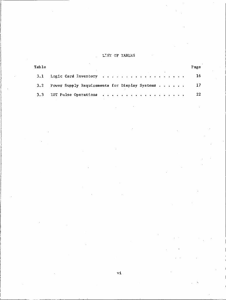
LIST OF TABLES
Table Page
3. ® X Logie Caird I%ive%ilLoiry © © © © o o © © © ® ® ® © © © ® © ® 16
3©2 Power Supply Requirements for Display Systems © © © © © © 17
3 © 3 IOT Pulse Operations © © © © © © © o © © © ® © © © © © ® 22
vi
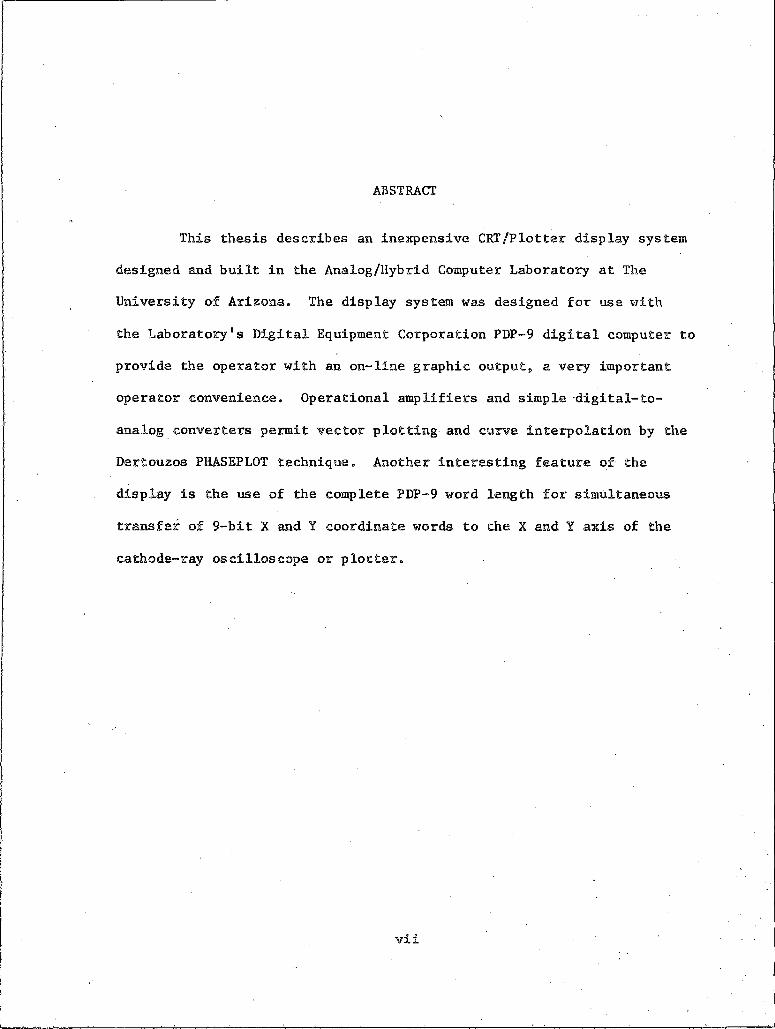
ABSTRACT
This thesis describes an inexpensive CRT/Plotter display system designed and built in the Analog/Hybrid Computer Laboratory at The University of Arizona. The display system was designed for use with
the Laboratory’s Digital Equipment Corporation PDP-9 digital computer to provide the operator with an on-line graphic output$ a very important operator convenience» Operational amplifiers and simple -digital-to-
analog converters permit vector plotting- and curve interpolation by the Dertouzos PHASE?LOT technique. Another interesting feature of the display is the use of the complete PDP-9 word length for simultaneous
transfer of 9-bit X and Y coordinate words to the X and Y axis of the
cathode-ray oscilloscope or plotter.
vii
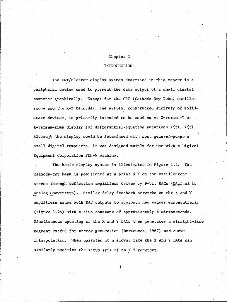
Chapter 1 INTRODUCTION
The CRT/Plotter display system described in this report is a
peripheral device used to present the data output of a small digital computer graphically® Except for the CRT (Cathode Ray Tube) oscilloscope and the X-Y recorder, the system, constructed entirely of solid-
state devices, is primarily intended to be used as an X-versus-Y or X-versus-time display for differential-equation solutions X(t), Y(t). Although the display could be interfaced with most general-purpose .small digital computers, it was designed mainly for use with a Digital
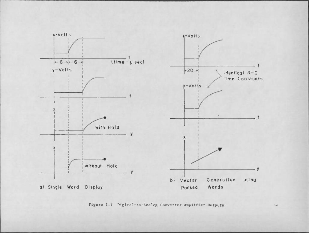
Equipment Corporation PDP-9 machine ®The basic display system is illustrated In Figure 1.1. The
cathode-ray beam is positioned at a point X-Y on the oscilloscope screen through deflection amplifiers driven by 9-bit DACs (Digital to Analog (Converters) * Similar delay feedback networks on the. X and Y 1 amplifiers cause both DAC outputs to approach new values exponentially
(Figure 1.2b) with a time constant of approximately 4 microseconds.
Simultaneous updating of the X and Y DACs then generates a straight-line
segment useful for vector generation (Dertouzos, 1967) and curve interpolation® When operated at a slower rate the X and Y DACs can
similarly position the servo axis of an X-Y recorder.
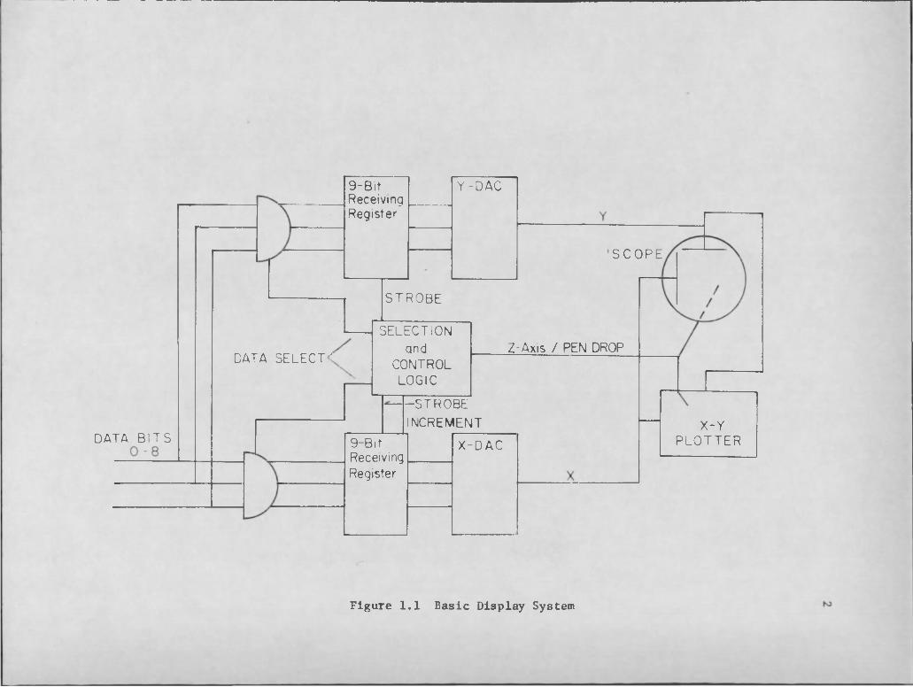
SC O P E
STROBE
Z-Axis / PEN DROPDATA SELECT"
-STR O BEINCREMENT
DATA B IT S 9-B itReceivingRegister
X-YPLOTTERX-DAC
9 -B itReceivingRegister
Y-DAC
SELECTIONand
CONTROLLOGIC
Figure 1.1 Basic Display System
x-Vol t s
( t i m e - [i sec)
y - V o l f s
with Hold
without Hold
a) Single Word Display
x-Vol ts
identical R - C Time Const an t s
y-Voi t ls
b) V e c t o r G e n e r a t i o n using
Packed Wor ds
Figure 1.2 Digital-to-Analog Converter Amplifier Outputs w
41.1 PDP-9 I/O Bus Interface
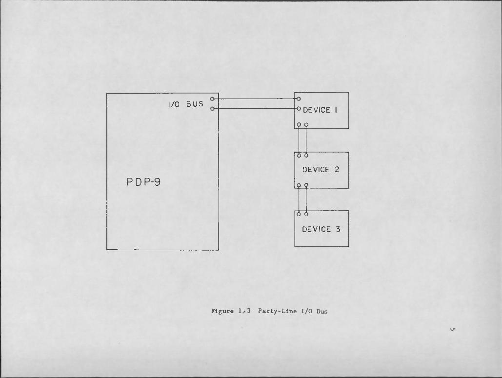
The PDP-9 interface preserves the parallel-mode of data-word transmission in the computer processor. It has a "party-line" I/O (Input/Output) buss of the general type shown in Figure 1.3, which conveniently provides for a variable number £>f peripheral devices« All peripheral devices are connected through I/O cables to the parallel- wired data bus. The latter is connected through a system of buffer registers to the computer accumulator register. The I/O cable contains
all communication links (data lines, control logic lines, subdevice lines, etc.) used between a device and the computer.
Device selection and control with programmable instructions for
a digital computer interface work with programed processing instructions
(Korn, 1968). The parallel connected device selection and control
lines of the PDP-9 correspond to the format of an I/O instruction word
in the processor instruction register (Digital Equipment Corporation,
1968). Control of up to 256 devices and generation of up to three
unique, commands for each of the 256 possible devices is obtainable with the IOT instruction capability of the PDP-9.
The PDP-9 I/O instruction word follows the format;
1. Bits 0-3 operation code 70,2. Bits 4 and 5 unused.
3. Bits 6-11 device selection.
4. Bits 12 and 13 subdevice selection. .
5. Bit 14 clear accumulator at event time one.6. Bit 15 generates IOP-4 command pulse at event time three.
I/O BUS
PDP-9
6 6
DEVICE 3
° DEVICE
Q Q
O 0
6 6DEVICE 2
Figure 1*3 Party-Line I/O Bus
7, Bit 16 generates IOP-2 command pulse at event time two;8„ Bit 17 generates IOP-1 command pulse at event time one.
In the display, the IOP pulses are regenerated for data-transfer strobing. Once the instruction word is recognized as an I/O output command, say for our displays
1. The contents of the accumulator appear on the I/O bus.2. The memory buffer (MB) issues a set of nine logic signalss
(a) A unique device selection code (MB 6-11)(b) Subdevice instruction (MB 12-13)(c) Command pulses (MB 15-17).
3. The contents of the memory buffer are transferred to the I/O bus.
Each peripheral device has at ,least one device selector, selectively wired to recognize a particular device selection code. The
device selector, essentially an AND gate, gates and regenerates the set of 1, 2, or 3 successive processor command pulses (IOP 1,2,4). These pulses, after regeneration by the device selector, are termed IOT (Input Output Transfer) pulses and are used to control data transfer
and other operations. The subdevice bits can further gate the command pulses, selecting device operating modes, and are also sufficient for selecting devices or subdevices.
1.2 Display Operating Modes
The principal modes of display operation, which can be selected
by the computer program are; '
1. Transfer bits 0-8 (Y) and bits 9-17 (X) from I/O bus to respective DAG registers, and display simultaneously (packed-
word operation). See Figure 1.2b.2. Transfer X from bits 0-8 of I/O bus into X-register. The
amplifier associated with the X DAG register is a traek-holdcircuit, which now holds the X-voltage. Next, Y is transferred
from bits 0-8 of I/O bus into the Y-register, then X and Y are
simultaneously displayed (Figure 1.2a).3. Transfer X from bits 0-8 of I/O bus into X-register and
display.4. Transfer Y from bits 0-8 of I/O bus into Y-register and
display.5. Transfer Y from bits 0-8 of I/O bus into Y-register, increment
the X-register, and display X and Y (curve plotting with
constant increments).
6. Control Z axis (trace brightness) of oscilloscope and pen drop. A one-bit register is used to turn trace either on or off.
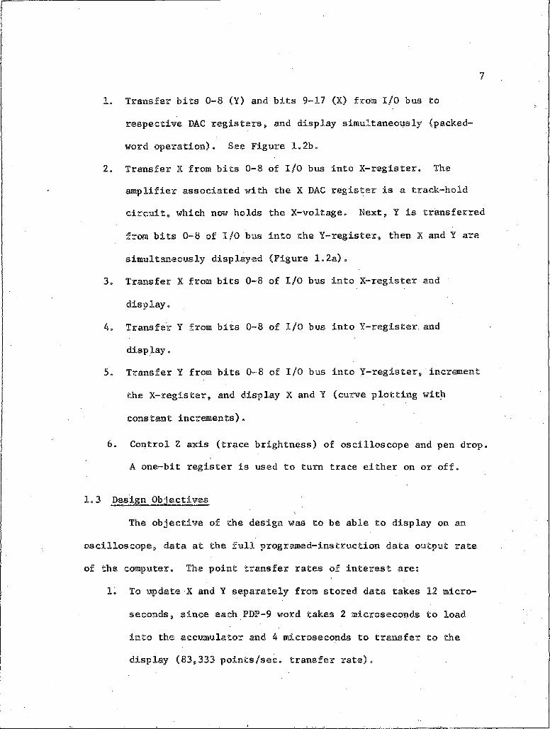
1.3 Design Objectives
The objective of the design was to be able to display on an
oscilloscope, data at the full programed-instruction data output rate of the computer. The point transfer rates of interest are:
1. To update X and Y separately from stored data takes 12 micro
seconds, since each PDP-9 word takes 2 microseconds to load
into the accumulator and 4 microseconds to transfer to thedisplay (83,333 points/sec. transfer rate).
8
2. To update X and Y simultaneously with a "packed" 18-bit word
similarly takes 6 microseconds (166,666 points/sec. transfer rate).
3. To pack and display (X,Y) , starting with separate X and Y words takes 20 microseconds with the instruction sequence (50,000
points/sec. transfer rate).
4. To increment X and transfer Y from storage (curve display) takes 6 microseconds (166,666 points/sec. transfer rate)«A typical four-curve display with word axis requires 1000 to
15000 points/second as determined by the minimum tolerable flicker rate of about 45 displays/second with a P-l phosphor.
The maximum available number of points/second should be limited by the rate at which the digital computer can transfer "packed" words (1 point every 6 microseconds) and not by the display electronics.
When outputting to an X-Y recorder the maximum data-transfer rate is determined by the slew rate of - the recorder. For the Hewlett Packard
7005A X-Y recorder used with this display, this was 15 inches/second. .
The resolution of the display system is governed primarily by the resolution of the DACs. Typically from 8 to 10 bit DAGs are
sufficient for good resolution. An 8 bit DAG gives a resolution of 1
part in 256, a 10 bit 1 part in 1024. A 9 bit DAG, giving a resolution
of 1 part in 512, was chosen. This was convenient for the packed word
scheme.

Chapter 2 SYSTEM DESIGN
Except for the large screen ITT oscilloscope and the I/O cable
needed tc connect the display to the PDP-9 computer, the system is
housed in a castered double relay rack„
As can be seen from Figure 2,1, the display consists primarily of two channels; one for the X-axis and one for the Y-axis. The two DAC channels are similar. The X channel can receive data from either
the first nine (0-8) or the last nine (9-17) data lines. The Y channel receives data only from the first nine (0-8) data lines. As shown, the output can be viewed on an oscilloscope or viewed and recorded on an
X-Y recorder at a much slower rate, "
2.2 Data TransferIn view of the similarity of the two channels $ it is simplest
to explain the data transfer between computer and display output recorded by considering one channel and noting the difference in the
other.On command, the data levels in the I/O bus are strobed into the
nine-bit receiving register. The system uses jam transfer, i.e., the
register does not have to be cleared between data transfers. Each
nine-bit receiving register is constructed of 3-C (Computer ̂ Control

Y - D A C
SCOR
STROBEDATA BITS
Hold
DATA Z-Axis / PEN DROP
SELECTHold
—STROBEINCREMENT
9-BitReceivingRegister
DATA BITS 9-17
X-YPLOTTER
Optional Hold and InterpolatingCircu it
Optional Hold and Interpolat-
Circuit
9 -B i tReceivingRegister
X - D A
SELECT and CONTROL LOGI C
Figure 2.1 System Block Diagram
11
jCompany) S-PAC flip-flop logic modules« Once a flip-flop is set it remains in the set mode until reset. Hence the receiving register can
be used as a temporary data storage device.The output of the receiving register is used to set the inputs
of the DAC (Mgital to Analog jConverter) . The output of the DAC feeds
the input of the. analog buffer.Each analog buffer is a track-hold and interpolating circuit
consisting of a pair of Burr-Brown operational amplifiers and an electronic switch.
The first operational amplifier matches the DAC impedance. The
second amplifier implements the exponential delay for line-segment generation. In addition, the second-amplifier also serves as a track-,
hold circuit or analog buffer to hold, say, X while Y is being fetched.
The switch is connected to the summing junction of the amplifier. The
time constant for the track-hold circuit depends upon which capacitor has been selected for the filter. The output of the second operational
amplifier is used to drive the axis of the CRT or the Plotting Board.The X-channel register is designed as a counter-register
(ripple-through counter) to permit incrementing of the X coordinate.The input to the counter can be switched to change the total number of
increments to 512, 256, 128, or 64,
2.3 Input Gating and Control Logic
The receiving registers use parallel information drop in. Modified 3-C NAND gates are used to supply the registers with data bits
and their complements. The gates have been modified, as explained in
12
Chapter 3, to serve as level changers between 3-C logic and the zero and minus three volt levels used by the DEC (Digital Equipment "jCorpora- tion) logic cards.
Besides the above mentioned gates, the X-axis uses a series of DEC NAND gates to select either the 9 high-order data-bus bits (for separate X and Y transfers) or the 9 low-order bits for packed-word transfers. Selection of these bits is controlled by the X-Y device
selector. When called, an assertion level from the device selector
inhibits the first nine data bits and allows the last nine through.When not called, the opposite is true.
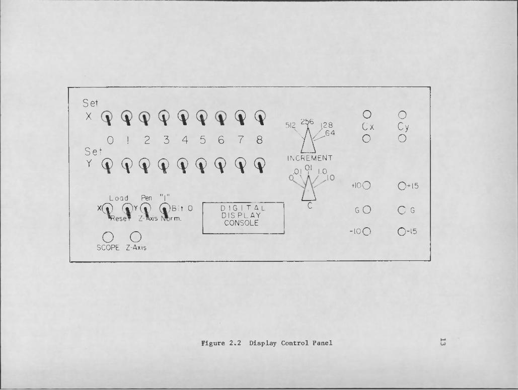
2.4 Display Control PanelFigure 2.2 depicts the display control panel. Panel switches
permit manual control of the following functions of the display:1. Presetting the DACs.2. Manually clearing the registers.
3. Manually loading the registers»
4. Control of the blanking of the Z-axis of the oscilloscope.,5. Control of the pen drop of the X-Y recorder.
6. Selection of the capacitor size for the low pass filter stage.
7. Selecting the increment .size for the ripple-through counter.
Except for items 6 and 7 the display can be entirely controlledby the PDP-9 computer. The panel switches are included as a simple
means for checking the operation of the display.
Set
x \ v (\' "A (%' ^ "̂v0 ! 2 3 4 5 6 7 8
SetY < ! > $ $ $ $ $ < * > $ < * >
L o a d Pen 111"
x ® ® Y ® ® 8 , t 0*Reser Z-axis rm.
O OSCOPE Z-Axis
DIGITALD I S P L A YCONSOLE
512 2^ 6 128
w
oCx0
0
CyO
L— \INCREMENT
.01 9 ' 1.0
t i o Q 0+15L— A
0 GO 0 G
-ioO 0 " I 5
Figure 2.2 Display Control Panel
2»5 Maintenance
The majority of the display system has been constructed in
modular form0 This simplifies troubleshooting in case of system
failure, since good modules can be easily‘inserted in place of
suspected bad ones* All digital and analog signals .are readily
available on the front of the mounting racks and can be viewed on an oscilloscope* Schematics for the system logic and circuitry can be
found in Chapter 3»
2 ® 6 Cost
The total cost of parts for the display system excluding the
oscilloscope and X-Y recorder was $2150,

Chapter 3 CIRCUIT DETAILS
The circuitry for the display system employs both Digital
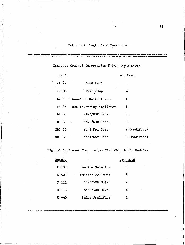
Equipment Corporation Flip-Chip Logic Modules (Digital Equipment
Corporations 1967) and Computer Control Company S-PAC Digital Modules (Computer Control Company, Inc., 1962)= Table 3.1 is an inventory of the logic cards used.
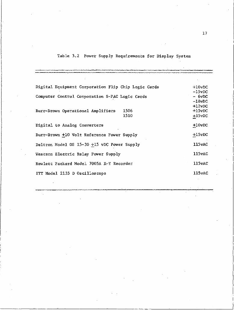
The power supply requirements for the display system are listed in Table 3.2. Current requirements were not included, but were considered maximum when computing power supply requirements.
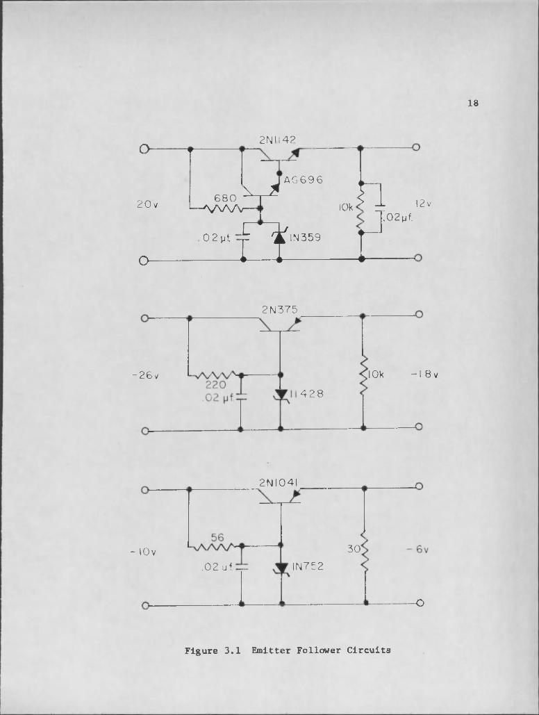
Figure 3.1 shows the emitter-follower circuits used to convert the Western Electric Relay Power Supplies into ones acceptable for supplying the 3-C logic cards.
All logic cards were mounted in racks using wire-wrap
connectors to facilitate construction. The analog buffers and DACs were built in the Hybrid/Analog Computer Laboratory.
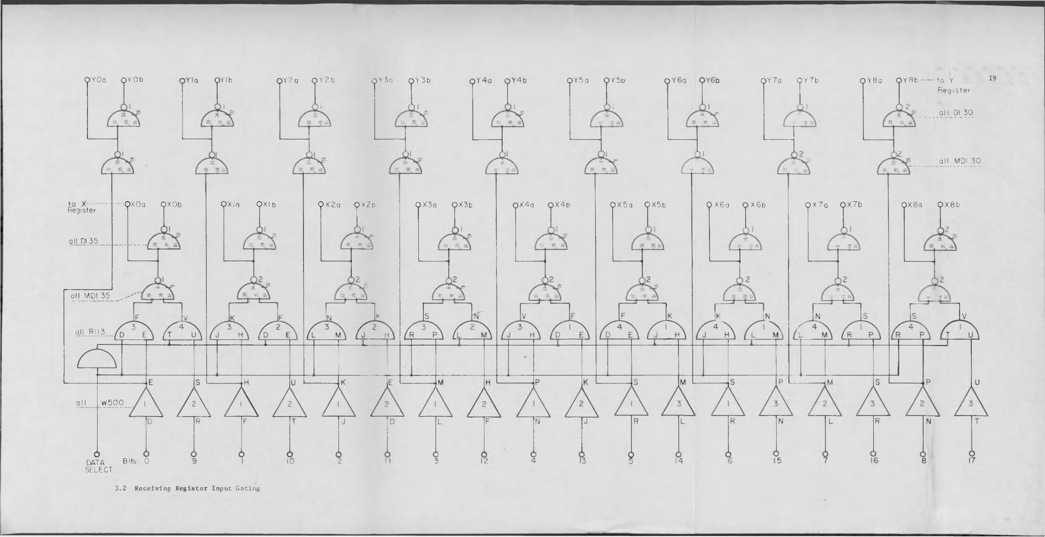
3.1 Register Input GatingFigure 3.2 is a schematic diagram of the input gating. The 18
input data lines are connected to DEC W500 emitter-follower modules.
Each W500 card contains 7 emitter-follower circuits.
Two sets of 9 each HAND gates (5 gates per R113 module) are
used to select which 9 data bits, 0-8 or 9-17, the X-register will
15
16
Table 3.1 Logic Card Inventory
Computer Control Corporation S-PAC Logic Cards
Card No, UsedUF 30 Flip-Flop 9
UF 35 Flip-Flop 1
DM 30 One-Shot Multivibrator 1PN 35 Non Inverting Amplifier 1DI 30 NAND/NOR Gate 3 .DI 35 NAND/N0R date 2
MDI 30 Nand/Nor Gate 2 (modified)
MDI 35 N'and/Nor Gate 2 (modified)
Ltal Equipment Corporation Flip Chip Logic Modules
Module No. UsedW 103 Device Selector 3
W 500 Emittter-Follcwer 3
R 111 NAND/NOR. Gate 2
R 113 NAND/NOR Gate 4 .
W 640 Pulse Amplifier 1
17
Table 3.2 Power Supply Requirements for Display System
Digital Equipment Corporation Flip Chip Logic Cards Computer Control Corporation S-PAC Logic Cards
Burr-Brown Operational Amplifiers 15061510
Digital to Analog Converters Burr-Brown 410 Volt Reference Power Supply
Deltron Model OS 15-30 +15 vDC Power Supply Western Electric Relay Power Supply Hewlett Packard Model 7005A X-Y Recorder
ITT Model 2135 D Oscilloscope
+10vDC -15vDC - 6vDC -18vDC +12vDC +15vDC +15vDC+10vDC+15vDC
115vAC115vAC
115vAC
115vAC
18
O 1
20v 6 8 0 — ' V W v
2 N I I4 2
J AGX J !
A G 6 9 6
10kn 12 v
0 2 pf. ' A IN359
O £2 ri 02pf.
2 N 3 7 5
I Ok- 2 6 v
4 2 8
-I 8 v
2 N I 0 4 I
30'- lOvIN752.0 2 uf.
— O
Figure 3.1 Emitter Follower Circuits
QYOo QYOb Q Y 2a O Y 2 b q Y 3 g Q Y 3 b Q Y 5 a Q Y5bOYIb Q Y 8 a Q Y 8 b ------- to YQY7a QY 7bReg is te r
al l Dl 30
al l MDI 3 0
QXOa QXOb QXia QX 7a Q X 7 bQ XIb Q X 2 a Q X 2 b Q X3a QX3b Q X 5 a Q X5b QX8a Q X 8 bQ X 4a Q X 4 b Q X6a Q X 6bRegister
all Dl 35
all MDI 35
all RI I3
W 5 0 0a l l
Bits 0DATASELECT
3.2 Receiving Register Input Gating
20receive. The assertion level (X-Y) from pin BD of the X-Y device selector is ANDed with gates 0-8. The complement (X-Y) of this level (output of a NOR gate) is ANDed with gates 9-17. When the X-Y device selector is called, the X-channel input registers receive data fromgates 9-17; when not called, from gates 0-8.
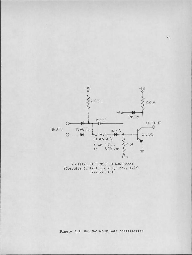
Input gating to the receiving registers was accomplished using
3-C DI-30 NAND/NOR gate pairs. The input registers used parallel
information drop in; therefore, the necessity for two gates. The first
gate of each pair was modified (see Figure 3.3) to accept the 0,-3 vdc
level of the DEC modules. The 3-C modules use 0,-6 volt levels. This modification was necessary to preserve the noise immunity of the .DI-30
gates.
Since the Y channel receives data only from bits 0-8, the only
gates needed were those .necessary to satisfy the parallel information
drop in.
3.2 Control Logic ,The control logic levels were obtained from the I0T pulses of
three DEC W103 device selectors. Table 3.3 lists the device selectors,
their device codes, and the uses of the associated TOT pulses.The NAND gates of the device selectors have been selectively
wired allowing them to see the necessary logical "Is" when called.
This involves inverting the logical "Os" of the particular device code.
Rill,cards were used for this inversion. Figure 3.4 schematically
represents the control logic, ‘
21
INPUTS
-18
6 4 9 k
IN9655 0 p f
OUTPUT
N965's IN8I6A a A / v — M — ^
CHANGED ^
f rom 2 2 6k ^ to 8 2 5 ohm <
2NI30I
21.5k
12 v
Modified DI30 (MDI30) NAND Pack (Computer Control Company, Inc., 1962)
Same as DI31
Figure 3.3 D-I NAND/NOR Gate Modification
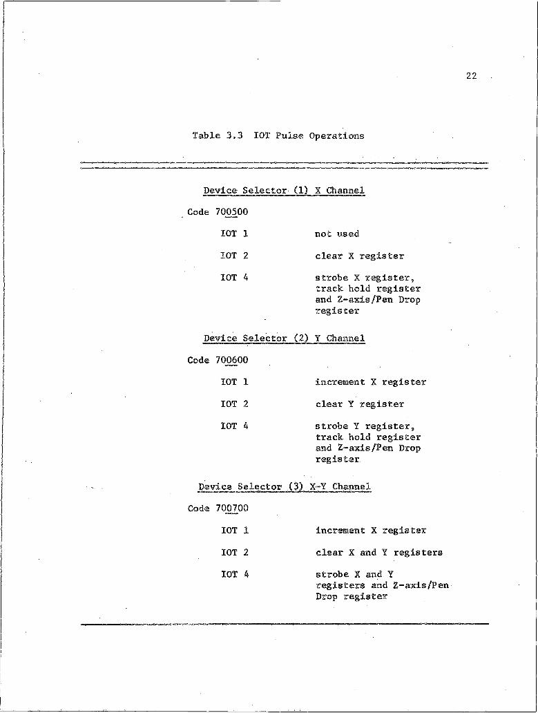
Table 3.3 IOT Pulse Operations
Device Selector (1) X ChannelCode 700500
IOT 1 not usedIOT 2 clear X registerIOT 4 strobe X register,
track hold register and Z-axis/Pen Drop register
Device Selector (2) Y ChannelCode 700600
IOT 1 increment X registerIOT 2 clear Y registerIOT 4 strobe Y register,
track hold register and Z-axis/Pen Drop register.
Device Selector (3) X-Y ChannelCode 700700
IOT 1 increment X registerIOT 2 clear X and Y registersIOT 4 strobe X and Y
registers and Z-axis/Pen Drop register

D I 30WI03 ■o CLEAR2 326
X-Y DMD IMDI 30-2
PN30Di 35-2WI03 WI03 INCREMENI 0 T I - Y 2 7
35 343 3 3 2
MDI 30-2WI03 I 0T4
X-Y 2 3 2 4 STROBE2 9
MDI 30-2WI0320
PN 3 0X - A x i s
Y
W I03
X-Y
WIO 3
I 0 T 4
d Tx DM30 \ 2 6 1 ,,30
2 3 p 2526 y - I I
7 bF / 1 5
MDI 30-2 1 4 3 1- 1 31 2
- 8 APN30
S T R O B E . -----------------o
WI03
W I03
MDI 3 0 -
Dl 30
1571 -Z
Y - A x i s
Figure 3.4 Control Logic
CLEAR
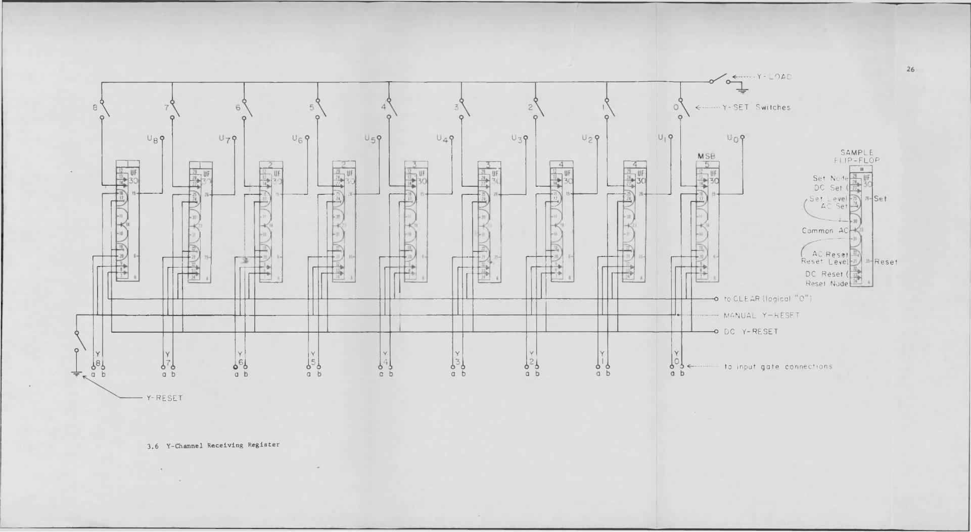
The X and Y channel receiving registers (Figures 3.5 and 3.6) were constructed from 3-C UF-30 flip-flop logic cards. There are nine flip-flops per channel. The UF-30 cards have two sets of AC as well as DC set and reset inputs and can operate at frequencies to 1 MHz.Control of the parallel information drop in is accomplished by use of
the IOT-4 pulse to strobe the AC gates. The set outputs connect to the input of the DACs. Common DC set and reset is provided. The XOT-2 pulse (1 microsecond) is used for common DC reset. Common DC set is manually controlled.
The minimum length of the strobe pulse necessary for the AC inputs is 1.6 microseconds. This was obtained by inputting the 400
nsee. IOT-4 pulse to a one-shot multi-vibrator (DM-30), boosting its
output through a non-inverting amplifier (PN-30) and using this regen
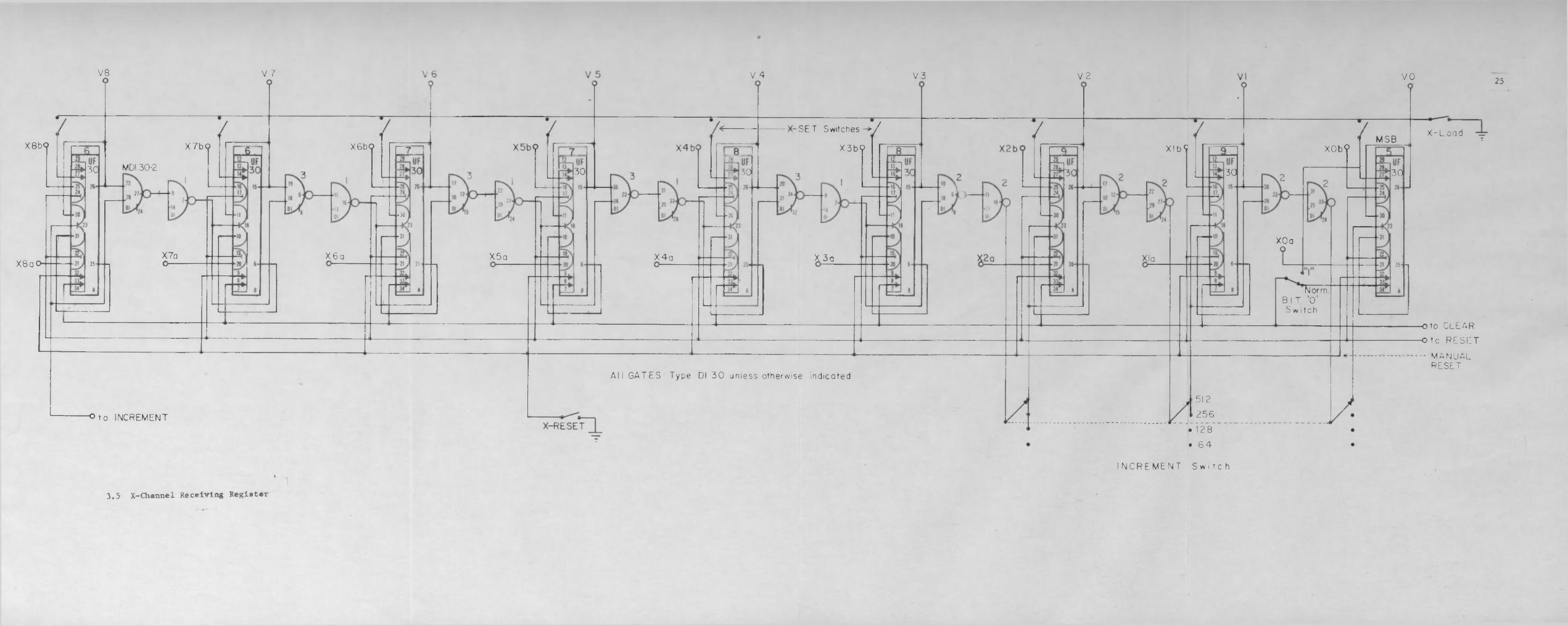
erated pulse for strobing.The X channel is also a ripple-through counter.' The counter is
controlled by IOT-1, X or X-Y. The pair of DI-30 gated between each
flip-flop allows the count to be carried forward when the command pulse
and the set output of the flip-flop are present. When the two levels (logical "Is") are not present the counter is disabled. The first gate
of the pair is used as an AND gate, the second a NOR gate.
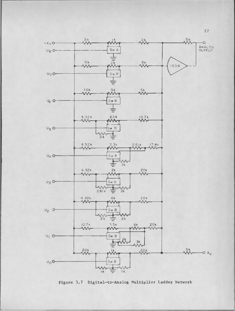
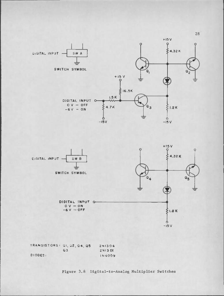
3.4 Digital to Analog ConvertersThe schematic diagram of the D/A ladder network and its asso
ciated dual-shunt switches are shown in Figure 3.7 and 3.8. A switch
V8 V 7 V 4 V 3 V 2 VO
SET Switches - > /
X3b9X - L o a d
MSBX8bQ X 7bO X6bO XI b 9 XOb?
MDI 30-230 30 301 30 30
-13■13 L_ .30>— -II I— -11I— -30
XOa
X7a X 6 a X5a X 4 a X 3a XlaX 8 a O 3 5 ---35- - - 35- -i
Klorm. B I T 'O' S w i tch
u ___
—O to CLEAR
—0 to RESET
— MANUAL RESET
A l l GATES Type Dl 3 0 unless otherwise indicated
512
2 5 6o to INCREMENT• 128
• 6 4
25
I N C R E M E N T S w i t c h
3.5 X-Channel Receiving Register
- Y - L O A D
X <- Y- SET Sw i tches
I - D25M 21ISA li
SAMPLEF L I P - F L O P
Set Node DC Set (
Se t Level AC Set
Common AC, -----AC Reset
Reset Level Rese t
DC Reset (Reset Node
o to CLEAR ( logica l 0 )
MANUAL Y - R E S F T
o DC Y -R E S E T
to input g a t e c o n n e c t io n s
Y -R E S E T
3.6 Y-Channel Receiving Register
27
- Xq o
1506
4 . 3 2 k 10 .7kA / V V
4 3 2 k A / W 3 3ky v wS w B
17.8 k
3k
4 . 3 2 k AA/v— f
S w B
2 0 kA Z W
10.7kAA/V
3.5kyvw 20 k6k
2 0 k
A/Ar-1
— Oa n a l o go u t p u t
Figure 3.7 Dig!ta1-to-Analog Multiplier Ladder Network
28f 15 V
4 . 32 KSW AD igital in p u t
SWI TCH SYMBOL
+ 15 V
6 . 5 K
DIGITAL I N P UT O- 0 V
- 6 V - ONOFF 4 . 7 K
- I 5 V -15 V
+ 15 V
4 . 3 2DIGITAL INPUT
SWITCH SYMBOL
D I GI T AL I N P U T 0 V - ON
- 6 V — OFF
SW B
-15 V
T R A N S I S T O R S ' 0 1 , ^ 2 , 0 4 , 0 3 2N 1 3 0 40 3 2 Ml 3 01
DIODES : I N 400<t
Figure 3.8 Digital-to-Analog Multiplier Switches
L

D I G I T A LI N P U T
5k
■ A / W -O OUTPUT
T r a n s i s t o r s
0 1 , 0 302
2N 3 2 4 2 A 2 N 4 i 2 6 SS 201215k
Diodes l O u f c a p a c i t o r #. SELECTOR ». EXT. CARI N 7 7 3 A
5 0 0 pf
0 O O I 5 p f15k
Q 3
11 k2 2k
l - V W17 k lOk
- I 5 v
Figure 3.9 Track-Hold Circuit
30
is connected at each A-B node on the ladder network which is in turn connected to a Burr-Brown 1506 operational amplifier.
The DACs, modified to include a ninth bit, are the ones originally used in ASTRAC II (Eckes, 1967).
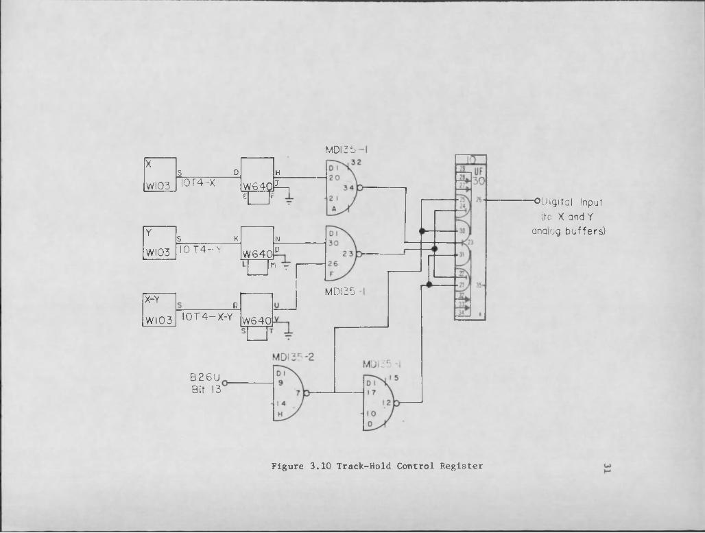
3.5 Track-Hold Circuit
The track-hdld circuit consisting of an electronic switch and a
1510 Burr-Brown operational amplifier is shown schematically in Figure
3.9. The switch is controlled by the output of a 1 bit register shown in Figure 3.10. The IOT-4 X or Y pulse is used to strobe the flip-flop
and subdevice bit 13 is complemented and serves as the data bit.
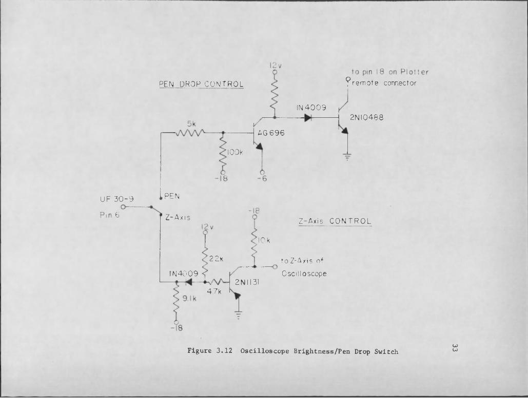
3.6 Oscilloscope Brightness and X-Y .Recorder Pen Drop Control
A simple one bit register shown in Figure 3.11 was used to control the oscilloscope brightness or the X-Y recorder pen drop.
The output of the register controls the brightness level control and pen drop electronic switch shown in Figure 3.12. The operator manually (Z-axis/Pen switch on display panel) selects which
mode is used depending on whether the oscilloscope or X-Y recorder is
used.
XS D H
WI03 !OT4-X W64Q I— iE F
Y S K NWI03 10 T 4 - Y W 6 4 0 P
M -
X-Y P
W I03 I 0 T 4 - X - Y W 640
B 2 6 U Bit 13
MDI2 5
MD135
■^Digital Input (to X and Y
analog buf fe rs )
Figure 3.10 Track-Hold Control Register

Y
WI03s o
W 640I 0 T 4 - YE F
X
W I03
S K
I 0 T 4 - X W640
WI03 I 0 T 4 - X - Y
B 2 S T Bit 12
MDI 35-
MDI 35-1
W640
MDI 35MDI 35-1
to■o Z-Axis / Pen Drop
Switch
3.11 Oscilloscope Brightness/Pen Drop Control Register wN)
UF 3 0 - 9
^ r e m o te connectorPEN DROP CONTROL
IN 4 0 0 92N I0 4 8 8
AG 6 9 6
100k
PEN
6 Z-Ax i
!0k
22k
N 4 0 0 92NII31
4.7k
Z-Ax is C O N T R O L
to Z-Axis of
Oscil loscope
Figure 3.12 Oscilloscope Brightness/Pen Drop Switch wu>
Chapter 4 RESULTS AND DISCUSSION
The main result of the project was the completed display circuitry providing the PDF-9 with an inexpensive CRT/Plotter display, a very important operator convenience.
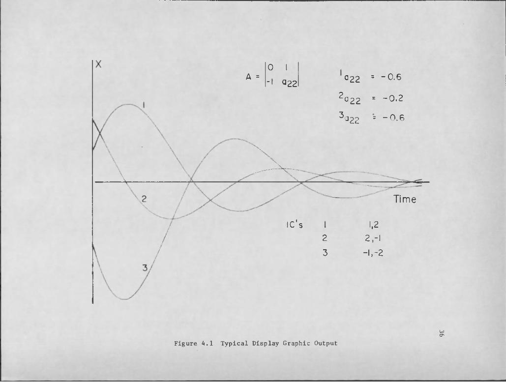
Figure 4,1 is a typical graphic output of the display system.It represents a set of solutions to a second-order system with varying
damping. This illustrates the importance of such a display system.The operator can view solutions to his problem while he is solving it on the computer system. This permits him to adjust system parameters,
while viewing the results, until the desired solution is achieved v
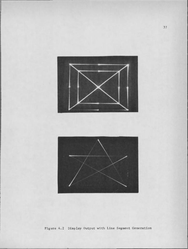
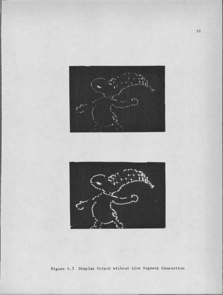
(on-line operation).Of interest also was the test of the Dertouzos line-segment
generation scheme with commercial amplifiers and simple DACs. Figures4.2 and 4.3 are examples of display output with and without line- segment generation.
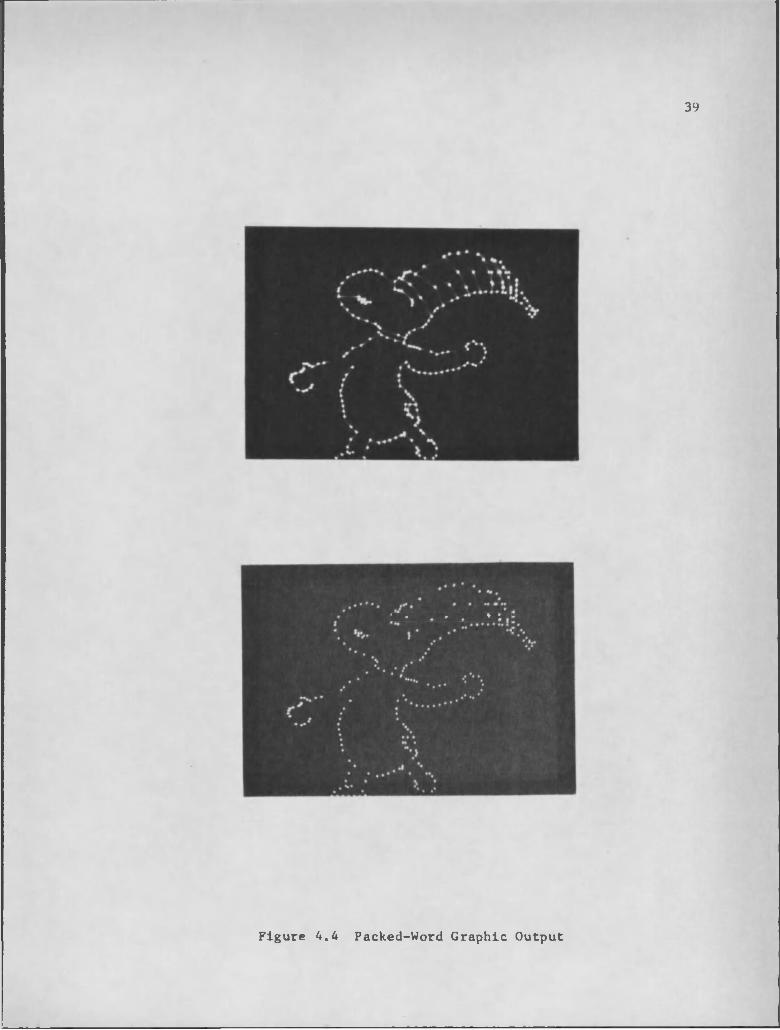
Of special importance was the implementation of the packed-word transfer scheme. The complete word.length (18 bits) of the PDP-9 is
split in two 9 bit bytes, one each for X and Y. This allows the X-Y data to be stored as a simple word and when displayed, transferred to both axes of the oscilloscope simultaneously. This method reduces the
number of memory locations needed for display storage by a factor of
one-half over display procedures using only 9 bits at a time, a
35significant saving of memory locations, and also improves the flicker rate. Figure 4.4 is a typical output using this mode of operation.
As a follow-on project an improved display will be built entirely of DEC logic for servicing convenience and lower costs. The '
operational amplifier track-hold circuit used to hold the X while Y is being transferred will be replaced by a digital buffer register. This will avoid drift and transients from the track-hold circuits and, as
integrated circuit logic becomes available, should actually be less expensive than the analog circuitry.
A =0 I -I 022 a 22 = ~ 0.6
^ u 2 2 = - 0.2
^□22 r “ 0.6
V
sx
^ N r —
//
IC's
Time
2
3
1,22,-1
- 1,-2
Figure 4.1 Typical Display Graphic OutputU)o
37
Figure A.2 Display Output with Line Segment Generation
^ V ♦- ♦ *
38
Figure 4.3 Display Output without Line Segment Generation
39
Figure 4.4 Packed-Word Graphic Output
REFERENCES
Computer Control Company9 Inc. "Instruction Manual for S-PAC Digital Modules," Publications No. 71-100A, Framingham, Massachusetts, April, 1962.
Digital Equipment Corporation. "Digital Logic Handbook," C-105,Maynard, Massachusetts, Copyright 1967.
. "Small Computer Handbook,," C-800, Maynard, Massachusetts, Copyright 1968.
Dertouzos, M. L. "PHASEPLOT: An Ota-line Graphical Display Technique,"IEEETEC, April, 1967.
Eekes, Harry R. "Design, Test, and Application of a High-speedIterative Differential Analyzer," Ph.D. Dissertation, Department of Electrical Engineering, University of Arizona, 1967.
Korn, G. A. "Digital Computer Interface System," ACL Memo 155,Department of Electrical Engineering, University of Arizona, June, 1968.
40