a finite element study of strain energy density...
TRANSCRIPT

Freescale™ and the Freescale logo are trademarks of Freescale Semiconductor, Inc. All other product or service names are the property of their respective owners. © Freescale Semiconductor, Inc. 2005.
TM
A Finite Element Study of Strain Energy Density DistributionNear A Triple Grain Junction and Its Implication on Whisker Growth
Third iNEMI Sn Whisker WorkshopMay 30, 2006
Peng Su and Min DingTechnology Solutions OrganizationFreescale Semiconductor Inc.

TM Freescale™ and the Freescale logo are trademarks of Freescale Semiconductor, Inc. All other product or service names are the property of their respective owners. © Freescale Semiconductor, Inc. 2005.
Peng Su, Ph.D. ([email protected])Slide 2
Outline
• Experimental• Test Condition
• -55ºC to 85ºC, 2000 cycles• Components:
• Sn-plated component strips (Assembly site 1)• Singulated 64LQFPs (Assembly site 1)• Singulated 100TQFPs (Assembly site 2)
• Materials:• Matte Sn, 10 µm nominal• CDA194 leadframe
• Microstructure observations after test
• Hypothesis and assumptions for the growth process
• Establishment of the finite element model
• Strain energy density (SED) distribution at grain-junctions
• First attempt at a predictive model for whisker growth

TM Freescale™ and the Freescale logo are trademarks of Freescale Semiconductor, Inc. All other product or service names are the property of their respective owners. © Freescale Semiconductor, Inc. 2005.
Peng Su, Ph.D. ([email protected])Slide 3
Microstructure Observations-1
• Component strips: Overview after AATC
“Beach pattern” and
recessed grains near whiskers
“Beach pattern” and
recessed grains near whiskers

TM Freescale™ and the Freescale logo are trademarks of Freescale Semiconductor, Inc. All other product or service names are the property of their respective owners. © Freescale Semiconductor, Inc. 2005.
Peng Su, Ph.D. ([email protected])Slide 4
Microstructure Observations-2
• 64LQFP: Overview after AATC
“Beach pattern” and
recessed grains near whiskers
“Beach pattern” and
recessed grains near whiskers

TM Freescale™ and the Freescale logo are trademarks of Freescale Semiconductor, Inc. All other product or service names are the property of their respective owners. © Freescale Semiconductor, Inc. 2005.
Peng Su, Ph.D. ([email protected])Slide 5
Microstructure Observations-3
• 100TQFP: Overview after AATC
“Beach pattern” and
recessed grains near whiskers
“Beach pattern” and
recessed grains near whiskers

TM Freescale™ and the Freescale logo are trademarks of Freescale Semiconductor, Inc. All other product or service names are the property of their respective owners. © Freescale Semiconductor, Inc. 2005.
Peng Su, Ph.D. ([email protected])Slide 6
Microstructure Observations-4
Recessed grains Strain / stress
concentration points?
• Magnified view of consumed grains near whiskers #1

TM Freescale™ and the Freescale logo are trademarks of Freescale Semiconductor, Inc. All other product or service names are the property of their respective owners. © Freescale Semiconductor, Inc. 2005.
Peng Su, Ph.D. ([email protected])Slide 7
Microstructure Observations-5
Whisker
“Beach”patterns
• Magnified view of consumed grains near whiskers #2

TM Freescale™ and the Freescale logo are trademarks of Freescale Semiconductor, Inc. All other product or service names are the property of their respective owners. © Freescale Semiconductor, Inc. 2005.
Peng Su, Ph.D. ([email protected])Slide 8
Microstructure Observations-6
“Beach Patterns”
• Magnified view of consumed grains near whiskers #3

TM Freescale™ and the Freescale logo are trademarks of Freescale Semiconductor, Inc. All other product or service names are the property of their respective owners. © Freescale Semiconductor, Inc. 2005.
Peng Su, Ph.D. ([email protected])Slide 9
Microstructure Observations-7
• Magnified view of consumed grains near whiskers #4
Whiskers
Recessed grains

TM Freescale™ and the Freescale logo are trademarks of Freescale Semiconductor, Inc. All other product or service names are the property of their respective owners. © Freescale Semiconductor, Inc. 2005.
Peng Su, Ph.D. ([email protected])Slide 10
Microstructure Observations-8
1. Fracture lines of an as-plated grain near the root of the whisker.
2. More ductile behavior of another grain next to the root of the whisker.

TM Freescale™ and the Freescale logo are trademarks of Freescale Semiconductor, Inc. All other product or service names are the property of their respective owners. © Freescale Semiconductor, Inc. 2005.
Peng Su, Ph.D. ([email protected])Slide 11
So How Are Whiskers Formed?
Step 1• Thermal strain / stress creates concentration points at grain boundaries or multi-grain junctions. The gradient of strain energy is higher if the one of the grains is very rigid.
(h1k1l1) (h2k2l2)
Step 2• High strain energy induces damage (fracture) to the weaker grain. The damage is worse at higher temperatures because Sn is more brittle.
(h1k1l1) (h2k2l2)
Step 3• Recovery and nucleation occur at these sites and forms whisker grains. Whisker grains may not have any orientation correlation with as-plated grains.
(h1k1l1) (h2k2l2)
Step 4• Surface diffusivity of the recessed grains is very high. Sn atoms travel along the surface (almost like sand) to the base of whiskers to support their continuous growth.• Certain grains in short distances may also diffuse to the growth site.
(h1k1l1) (h2k2l2)
Step 5• The original as-plated grain may be completely consumed at long test durations. Whisker’s growth may slowly saturate or stop.
(h1k1l1) (h2k2l2)

TM Freescale™ and the Freescale logo are trademarks of Freescale Semiconductor, Inc. All other product or service names are the property of their respective owners. © Freescale Semiconductor, Inc. 2005.
Peng Su, Ph.D. ([email protected])Slide 12
Hypothesis and Assumptions
• The significance of grain orientations• Whiskers only nucleate and grow near certain grains. While these grains can be consumed very quickly by
the growth of whiskers, some of the immediate neighboring grains often do not experience any damage.
• Grain orientations are the most probable caused that induces such differences.
• Sn is very anisotropic. Mechanical properties along different planes and directions can be very different.
• A growth model does not necessarily need to address long-range damage and diffusion activities. Groups or pairs of Sn grains can be treated as discrete samples and analyzed separately.
• Assumptions for the finite element model • The goal of the model is to answer the question: Which grain boundary or grain junctions is mostly likely to
whisker?
• We only need to identify the strain energy distribution prior to the actual damage / whisker growth occurs. Thus plasticity does not need to be calculated.
• It is assumed that higher strain energy density will correlate to high possibility of whisker growth.
• Grain orientations are assigned based on XRD analysis.
• Grains are horizontally rotated along the surface and strain energy is calculated for each rotation.

TM Freescale™ and the Freescale logo are trademarks of Freescale Semiconductor, Inc. All other product or service names are the property of their respective owners. © Freescale Semiconductor, Inc. 2005.
Peng Su, Ph.D. ([email protected])Slide 13
Geometry of the Model
As-platedSn grain structure(after FIB)
Grain structurein finite element model
(h1k1l1)
Grains simulated in this model
The focus is to investigate the effects of rotation on strain energy levels
(h2k2l2)
(h3k3l3)

TM Freescale™ and the Freescale logo are trademarks of Freescale Semiconductor, Inc. All other product or service names are the property of their respective owners. © Freescale Semiconductor, Inc. 2005.
Peng Su, Ph.D. ([email protected])Slide 14
Material Properties
• Basic properties• Sn thickness is 10µm, Cu thickness is 50 µm.• Published stiffness matrix is used for Sn. Cu is assumed to be
mechanically isotropic.• Elements are pure elastic.• Two sides of the Sn+Cu stack are fixed. The other two sides are
coupled to ensure equivalent displacements.• Top and bottom surfaces are both free.
• Grain orientations• The horizontal plane systems of as-plated Sn finish can be determined with X-ray diffraction. (*)• Three arbitrary orientations are selected for the model.
20 30 40 50 60 70 80 90 100 110 120
(220) (211) (321)
(431)
2 Theta

TM Freescale™ and the Freescale logo are trademarks of Freescale Semiconductor, Inc. All other product or service names are the property of their respective owners. © Freescale Semiconductor, Inc. 2005.
Peng Su, Ph.D. ([email protected])Slide 15
Why Not Compare Stresses?
• Stress distribution (arbitrary grain orientation, all 6 stress components)
xσ yσ zσ
xyτ yzτ xzτ

TM Freescale™ and the Freescale logo are trademarks of Freescale Semiconductor, Inc. All other product or service names are the property of their respective owners. © Freescale Semiconductor, Inc. 2005.
Peng Su, Ph.D. ([email protected])Slide 16
The Convenience of Using Energy
• Total strain energy density (SED) of a generalized stress state
( )xzxzyzyzxyxyzzyyxxU γτγτγτεσεσεσ +++++=21
[ ]
[ ]
[ ]
zxzx
yzyz
xyxy
yyxxzzzz
xxzzyyyy
zzyyxxxx
E
E
E
E
E
E
σνγ
σνγ
σνγ
σσνσε
σσνσε
σσνσε
)1(2
)1(2
)1(2
)(1
)(1
)(1
+=
+=
+=
+−=
+−=
+−=y
x
δ
y
x
τxy
γxy

TM Freescale™ and the Freescale logo are trademarks of Freescale Semiconductor, Inc. All other product or service names are the property of their respective owners. © Freescale Semiconductor, Inc. 2005.
Peng Su, Ph.D. ([email protected])Slide 17
Steps of Simulation
• We will individually rotate the 3 grains and calculate the SED levels in the 3-grain system.• The three horizontal plane systems are arbitrarily chosen as (112), (321), and (220)• Each grain is individually rotated in 20º steps. After each rotation, the SED of the entire system and the
junction of the grains (circled below) are compared.
(220) (112)
(321)
-55ºC to 85ºC
X
YZ
XY
Z
X
YZ
SED

TM Freescale™ and the Freescale logo are trademarks of Freescale Semiconductor, Inc. All other product or service names are the property of their respective owners. © Freescale Semiconductor, Inc. 2005.
Peng Su, Ph.D. ([email protected])Slide 18
Effects of Rotation on Total and Center SED
• For the selected grain orientation configuration, horizontal rotation of the grains does not have a significant impact on the total SED of the system (blue lines).
• However the triple-grain junction is significantly affected by the rotation angles (purple lines).
• The rotation of the (220) grains has the highest impact on the grain junction.
• The rotation of the (112) grain also has an obvious effect on the total and center SED.
• The rotation of the (321) grain has very non-symmetrical impact on the total and central SED.
0.20
0.30
0.40
0.50
0 50 100 150 200 250 300 350 400Rotation Angles
SED
(Arb
itrar
y Un
it)
Total SED
Center SED
Rotation of (112)
0.10
0.20
0.30
0.40
0.50
0 50 100 150 200 250 300 350 400Rotation Angles
SED
(Arb
itrar
y U
nit)
Total SED
Center SED
Rotation of (321)
0.20
0.30
0.40
0.50
0 50 100 150 200 250 300 350 400Rotation Angles
SED
(Arb
itrar
y U
nit)
Total SED
Center SED Rotation of (220)

TM Freescale™ and the Freescale logo are trademarks of Freescale Semiconductor, Inc. All other product or service names are the property of their respective owners. © Freescale Semiconductor, Inc. 2005.
Peng Su, Ph.D. ([email protected])Slide 19
SED Gradient of Each Rotation
• A parameter Alpha is defined as
• Clearly when the (220) grain is rotated to certain angles, it induces a high SED in the triple-grain junction.
0.0
0.5
1.0
1.5
0 50 100 150 200 250 300 350 400Rotation Angles
Alp
ha
(112) Alpha(321) Alpha(220) Alpha
Total
center
SEDSED
Alpha =

TM Freescale™ and the Freescale logo are trademarks of Freescale Semiconductor, Inc. All other product or service names are the property of their respective owners. © Freescale Semiconductor, Inc. 2005.
Peng Su, Ph.D. ([email protected])Slide 20
The Effects of Rotation on Each Individual Grain
• Here we plot the SED in each of the 3 grains at each of the rotation angles.
• Again the (220) grain has the most significant modulating effect on the neighboring grains. Each rotation of the (220) grain induces strong reaction in itself and the other 2 grains.
• The rotation of (112) grain has certain effect on the other 2 grains.
• The rotation of (321) grain does not have a strong effect on either itself or the neighboring grains.
0.0E+00
5.0E-07
1.0E-06
1.5E-06
2.0E-06
2.5E-06
3.0E-06
0 50 100 150 200 250 300 350 400Rotation Angles
SE
D (A
rbitr
ary
Uni
t)
(220) SED Total
(112) SED Total(321) SED Total
Rotation of (321)
0.0E+00
5.0E-07
1.0E-06
1.5E-06
2.0E-06
2.5E-06
3.0E-06
0 50 100 150 200 250 300 350 400Rotation Angles
SE
D (A
rbitr
ary
Uni
t)
(220) SED Total(112) SED Total(321) SED Total
Rotation of (220)
0.0E+00
5.0E-07
1.0E-06
1.5E-06
2.0E-06
2.5E-06
3.0E-06
0 50 100 150 200 250 300 350 400Rotation Angles
SED
(Arb
itrar
y U
nit)
(220) SED Total(112) SED Total(321) SED Total
Rotation of (112)
TM Freescale™ and the Freescale logo are trademarks of Freescale Semiconductor, Inc. All other product or service names are the property of their respective owners. © Freescale Semiconductor, Inc. 2005.
Peng Su, Ph.D. ([email protected])Slide 21
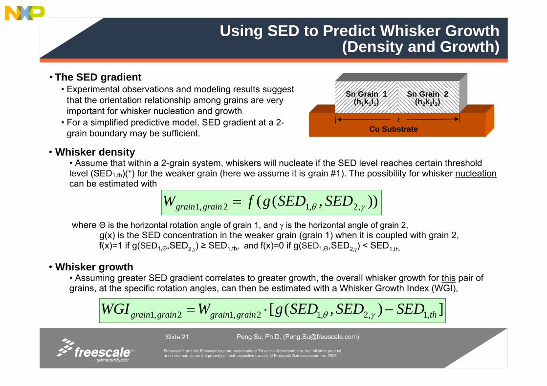
• Whisker density• Assume that within a 2-grain system, whiskers will nucleate if the SED level reaches certain threshold level (SED1,th)(*) for the weaker grain (here we assume it is grain #1). The possibility for whisker nucleationcan be estimated with
where Θ is the horizontal rotation angle of grain 1, and γ is the horizontal angle of grain 2,g(x) is the SED concentration in the weaker grain (grain 1) when it is coupled with grain 2,f(x)=1 if g(SED1,Θ,SED2,γ) ≥ SED1,th, and f(x)=0 if g(SED1,Θ,SED2,γ) < SED1,th.
• Whisker growth• Assuming greater SED gradient correlates to greater growth, the overall whisker growth for this pair of grains, at the specific rotation angles, can then be estimated with a Whisker Growth Index (WGI),
Using SED to Predict Whisker Growth(Density and Growth)
• The SED gradient• Experimental observations and modeling results suggest
that the orientation relationship among grains are very important for whisker nucleation and growth
• For a simplified predictive model, SED gradient at a 2-grain boundary may be sufficient. Cu Substrate
Sn Grain 1(h1k1l1)
Sn Grain 2(h2k2l2)
ε
)),(( ,2,12,1 γθ SEDSEDgfW graingrain =
]),([ ,1,2,12,12,1 thgraingraingraingrain SEDSEDSEDgWWGI −⋅= γθ

TM Freescale™ and the Freescale logo are trademarks of Freescale Semiconductor, Inc. All other product or service names are the property of their respective owners. © Freescale Semiconductor, Inc. 2005.
Peng Su, Ph.D. ([email protected])Slide 22
Whisker Growth Propensity of a 2-Grain System
• Calculating the average whisker growth rate• SED in a 2-grain system of any orientation can be
readily calculated with the finite element model.• The W and WGI of a specific pairing configuration can
be estimated with ( i denotes this particular pairing)
0.0E+00
5.0E-07
1.0E-06
1.5E-06
2.0E-06
2.5E-06
0 100 200 300 400Rotation Angles
SED
(Arb
itrar
y U
nit)
Grain 1Grain 2
0.0E+00
5.0E-07
1.0E-06
1.5E-06
2.0E-06
2.5E-06
0 100 200 300 400Rotation Angles
SED
(Arb
itrar
y U
nit)
Grain 1Grain 2
0.0E+00
1.0E-06
2.0E-06
3.0E-06
4.0E-06
5.0E-06
0 100 200 300 400Rotation Angles
SED
(Arb
itrar
y U
nit)
Grain 1
Grain 2
Grain Pair Example #1
Grain Pair Example #2
Grain Pair Example #3
γθθ γ
γθ ddSEDSEDgfWi ⋅⋅−= ∫ ∫= =
))((360
0
360
0,2,1
γθθθ γ
ddSEDSEDWWGI thii ⋅⋅−⋅= ∫ ∫= =
)( ,1,1
360
0
360
0
Rotation of Grain 2 only
Rotation of Grain 2 only

TM Freescale™ and the Freescale logo are trademarks of Freescale Semiconductor, Inc. All other product or service names are the property of their respective owners. © Freescale Semiconductor, Inc. 2005.
Peng Su, Ph.D. ([email protected])Slide 23
Calculate Pairing Possibilities
• Calculation of pair combinations• If we have a macro-view of the orientation information, we can calculate the pairing possibilities.
120.5940.8868( 3 2 3)114.1260.9178( 6 1 1)113.3430.9219( 6 2 0)112.0960.9286( 5 1 2)111.6590.931( 3 0 3)104.8640.9718( 6 0 0)103.2710.9824( 2 1 3)97.4141.0252( 5 2 1)96.6951.0309( 4 4 0)95.5621.0401( 3 3 2)95.1631.0434( 1 0 3)89.4091.095( 4 3 1)
13%79.471.205( 3 1 2)8.5%73.1951.292( 4 1 1)
72.4141.304( 4 2 0)30%64.5761.442( 3 2 1)
63.7831.458( 4 0 0)30%62.5381.484( 1 1 2)
55.331.659( 3 0 1)3.5%44.9022.017( 2 1 1)15%43.8712.062( 2 2 0)
32.0182.793( 1 0 1)30.6442.915( 2 0 0)
%2 Thetad( h k l)
If the orientation mix looks like this
0.0%
5.0%
10.0%
15.0%
20.0%
(220
)-(41
1)
(220
)-(31
2)
(220
)-(22
0)
(220
)-(21
1)
(220
)-(11
2)
(220
)-(32
1)
(211
)-(41
1)
(211
)-(31
2)
(211
)-(21
1)
(211
)-(11
2)
(211
)-(32
1)
(112
)-(41
1)
(112
)-(31
2)
(112
)-(11
2)
(112
)-(32
1)
(321
)-(41
1)
(321
)-(31
2)
(321
)-(32
1)
(411
)-(41
1)
(411
)-(31
2)
(312
)-(31
2)
pair
%
The pair mix looks like this (Monte-Carlo method)
AN EXAMPLE

TM Freescale™ and the Freescale logo are trademarks of Freescale Semiconductor, Inc. All other product or service names are the property of their respective owners. © Freescale Semiconductor, Inc. 2005.
Peng Su, Ph.D. ([email protected])Slide 24
Whisker Growth Propensity of the Entire System
• Whisker density• We have calculated the average possibility of whisker nucleation, Wi, for a specific paring configuration.• We also calculated the percentage of each pair of the total paring possibilities. • The density of whiskers can then be estimated with
where pi is the probability of the specific pairing i, n is the total number of possible pairing.
• Whisker growth rate• Similarly, we have estimates the growth rate for each specific paring, WGIi.• Utilize the probability of each pairing pi, the total WGI of the system is then
)(1
i
n
iitotal pWW ⋅= ∑
=
)(1
i
n
iitotal pWGIWGI ⋅= ∑
=
• Verification of W and WGI• Initial success: Freescale data, published data• More detailed microstructure information, particularly near whiskers, will help to improve the accuracy of
the predictive models.• Whisker testing needs to be done with non-formed components strips.
• Forming process introduces mechanical damage and stress into Cu and Sn layers.• Complete whisker population data after test (more than just longest whisker) is also necessary.

TM Freescale™ and the Freescale logo are trademarks of Freescale Semiconductor, Inc. All other product or service names are the property of their respective owners. © Freescale Semiconductor, Inc. 2005.
Peng Su, Ph.D. ([email protected])Slide 25
Summary and Further Work
• Experimental observations• During the AATC test, whisker growth appears to be strongly associated with neighboring grains that have
specific crystallographic orientations.• These grains are likely under higher strain / stress compared with the rest of the Sn finish, due to Sn’s
mechanical anisotropy.• These grains also have very high surface diffusivity, which further assists the growth of whiskers.
• Finite element modeling• Investigation of additional grain orientation mixes and SED
distribution characterization is planned.• Effects of other material variations such as thickness (on-going),
substrate, and grain geometries needs to be investigated.• Effects of other stressing situations, such as vertical indentation
and stress from IMC growth will be studied.
• First attempt at a predictive model• The WGI parameter has provided initial success in correlating
microstructure to whisker growth.• Further experimental and simulation work will help improve the
precision of such predictive model. Orientation measurement with techniques such as EBSD will be beneficial.
• With certain modifications, such model can also be used at situations with different stress origins.
Whisker Growth on SnPb Finish
2-phase whiskers, recessed grains

TM Freescale™ and the Freescale logo are trademarks of Freescale Semiconductor, Inc. All other product or service names are the property of their respective owners. © Freescale Semiconductor, Inc. 2005.