a genetic algorithm for the design of passive filters and ...tcc/georgasbascthesisda.pdf · a...
TRANSCRIPT

A Genetic Algorithm for the Design of Passive Filtersand a Distributed Amplifier
by
Michael Georgas
A THESIS SUBMITTED IN PARTIAL FULFILLMENTOF THE REQUIREMENTS FOR THE DEGREE OF
BACHELOR OF APPLIED SCIENCE
Division of Engineering Science
FACULTY OF APPLIED SCIENCE AND ENGINEERINGUNIVERSITY OF TORONTO
Supervisor: Professor Anthony Chan Carusone
April 13, 2007

i
Abstract
A genetic algorithm for the design of passive filters and a distributed amplifier is presented.The characteristics of the algorithm are studied through simple design examples that includea resistor divider, a T-filter, and a 5th-order low-pass filter. In each case, the algorithm isable to meet all of the performance requirements. Preliminary results from the design ofa distributed amplifier are presented. While the algorithm does not design an amplifierthat meets the performance requirements within a reasonable design time, analysis of theevolution indicates that the design does improve with each generation. This demonstratesthat the algorithm is able to evolve the circuit to meet the specification.

ii
Acknowledgements
I would first like to thank Professor Anthony Chan Carusone for his guidance and supportover this past year. My experience within his group has left a tremendously positive impacton me and has shaped my future ambitions. I would also like to thank my family for theirever-present support, and Diana for always believing in me. Finally, I would like to thankthe classmates with whom I have shared the past four years.
CONTENTS
1. Introduction . . . . . . . . . . . . . . . . . . . . . . . . . . . . . . . . . . . . . . . 1
1.1 Motivation . . . . . . . . . . . . . . . . . . . . . . . . . . . . . . . . . . . . . 1
1.2 Background . . . . . . . . . . . . . . . . . . . . . . . . . . . . . . . . . . . . 2
1.2.1 Genetic Algorithms . . . . . . . . . . . . . . . . . . . . . . . . . . . . 2
1.2.2 Wideband Communications . . . . . . . . . . . . . . . . . . . . . . . 3
2. Genetic Algorithm Implementation . . . . . . . . . . . . . . . . . . . . . . . . . . 6
2.1 Cost Function . . . . . . . . . . . . . . . . . . . . . . . . . . . . . . . . . . . 6
2.2 Mutation . . . . . . . . . . . . . . . . . . . . . . . . . . . . . . . . . . . . . . 7
3. Filter Examples . . . . . . . . . . . . . . . . . . . . . . . . . . . . . . . . . . . . . 9
3.1 Resistor Divider . . . . . . . . . . . . . . . . . . . . . . . . . . . . . . . . . . 9
3.1.1 Experiment . . . . . . . . . . . . . . . . . . . . . . . . . . . . . . . . 10
3.2 T-Filter . . . . . . . . . . . . . . . . . . . . . . . . . . . . . . . . . . . . . . 13
3.2.1 Experiment . . . . . . . . . . . . . . . . . . . . . . . . . . . . . . . . 14
3.3 Higher-Order Filter Design . . . . . . . . . . . . . . . . . . . . . . . . . . . . 18
3.3.1 Experiment . . . . . . . . . . . . . . . . . . . . . . . . . . . . . . . . 19
4. Genetic Algorithm for Distributed Amplifier Design . . . . . . . . . . . . . . . . . 24
4.1 Experiment . . . . . . . . . . . . . . . . . . . . . . . . . . . . . . . . . . . . 25
5. Conclusion . . . . . . . . . . . . . . . . . . . . . . . . . . . . . . . . . . . . . . . . 29
5.1 Future Work . . . . . . . . . . . . . . . . . . . . . . . . . . . . . . . . . . . . 29
Appendix 31
A. ABCD Matrices . . . . . . . . . . . . . . . . . . . . . . . . . . . . . . . . . . . . . 32
Contents iv
B. T-Model Analysis . . . . . . . . . . . . . . . . . . . . . . . . . . . . . . . . . . . . 34
C. Maximally Flat Design Using Filter Prototype Method . . . . . . . . . . . . . . . 36
D. Distributed Amplifier S-parameter Derivation . . . . . . . . . . . . . . . . . . . . 38
E. Hand Design of a Distributed Amplifier . . . . . . . . . . . . . . . . . . . . . . . . 41
LIST OF FIGURES
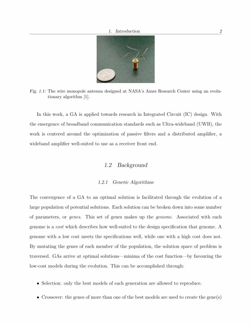
1.1 The wire monopole antenna designed at NASA’s Ames Research Center usingan evolutionary algorithm [1]. . . . . . . . . . . . . . . . . . . . . . . . . . . 2
1.2 CMOS Common-gate Input Stage . . . . . . . . . . . . . . . . . . . . . . . . 4
1.3 Transmission Line Implementation of a Distributed Amplifier . . . . . . . . . 4
3.1 Resistor Divider . . . . . . . . . . . . . . . . . . . . . . . . . . . . . . . . . . 9
3.2 The evolution of the resistances in order to produce and output voltage of 3Vwith a power dissipation of 100mW . . . . . . . . . . . . . . . . . . . . . . . 11
3.3 The effect of changing the resistor divider specification weights on the perfor-mance. . . . . . . . . . . . . . . . . . . . . . . . . . . . . . . . . . . . . . . . 12
3.4 The effect of changing the resistor divider specification weights on the perfor-mance. . . . . . . . . . . . . . . . . . . . . . . . . . . . . . . . . . . . . . . . 12
3.5 Low-pass T-filter . . . . . . . . . . . . . . . . . . . . . . . . . . . . . . . . . 13
3.6 The effect of changing the T-filter specification weights on the performance. . 15
3.7 The effect of changing the T-filter specification weights on the cost. . . . . . 15
3.8 The effect of changing the T-Filter specification weights on the performance. 17
3.9 The effect of changing the T-Filter specification weights on the cost. . . . . . 17
3.10 S-parameter plots for the T-filters designed by the genetic algorithm. . . . . 18
3.11 Three-stage low-pass filter. . . . . . . . . . . . . . . . . . . . . . . . . . . . . 18
3.12 The figure shows the effect of the generation on the cost function of the algo-rithm. . . . . . . . . . . . . . . . . . . . . . . . . . . . . . . . . . . . . . . . 20
3.13 The performance plots for each of the 5th order filters designed by the GA. . 22
3.14 The S-parameter plots for each of the 5th order filters designed by the GA. . 23
4.1 The model for a single stage of the distributed amplifier. . . . . . . . . . . . 25
4.2 Performance of the genetic algorithm on the distributed amplifier. . . . . . . 26
4.3 S-parameter plots for distributed amplifiers designed by the GA and by hand. 28
A.1 The ABCD matrix of a 2-Port Netork . . . . . . . . . . . . . . . . . . . . . . 32
List of Figures vi
B.1 The T-equivalent Model of a 2-Port Network . . . . . . . . . . . . . . . . . . 34
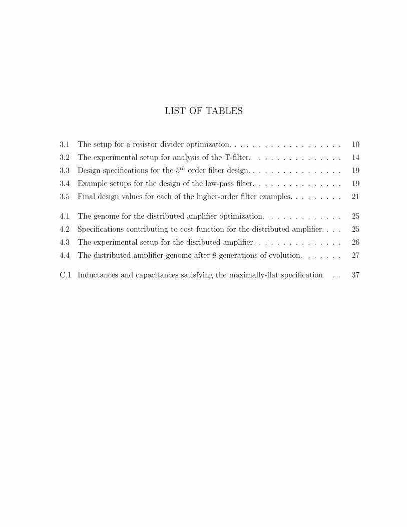
LIST OF TABLES
3.1 The setup for a resistor divider optimization. . . . . . . . . . . . . . . . . . . 10
3.2 The experimental setup for analysis of the T-filter. . . . . . . . . . . . . . . 14
3.3 Design specifications for the 5th order filter design. . . . . . . . . . . . . . . . 19
3.4 Example setups for the design of the low-pass filter. . . . . . . . . . . . . . . 19
3.5 Final design values for each of the higher-order filter examples. . . . . . . . . 21
4.1 The genome for the distributed amplifier optimization. . . . . . . . . . . . . 25
4.2 Specifications contributing to cost function for the distributed amplifier. . . . 25
4.3 The experimental setup for the disributed amplifier. . . . . . . . . . . . . . . 26
4.4 The distributed amplifier genome after 8 generations of evolution. . . . . . . 27
C.1 Inductances and capacitances satisfying the maximally-flat specification. . . 37

1. INTRODUCTION
1.1 Motivation
The use of a Genetic Algorithm (GA) in this work was inspired by recent work in electrical
engineering and computer science. GAs are often used to solve a problem where there is
little knowledge of what the solution will look like. These solutions may be non-intuitive or
not easily derivable by the designer. GAs can also be used to fine tune a solution once the
parameters have been roughly set. In this work, a GA is applied to the design of passive filters
and a distributed amplifier. While simple filters are easily analyzed using hand calculations,
in order to meet more demanding specifications, filters of higher order are required. The
design of such filters is not easily accomplished by hand, especially for a less-experienced
designer.
One area where GAs have found a number of applications is in the field of electromagnetics
and Radio Frequency (RF) communications. In 2004, a computer scientist at the NASA
Ames Research Center presented a monopole wire antenna that was designed to meet a
specification for the Space Technology 5 spacecraft. The significance of this contribution
lies not only in the fact that an evolutionary algorithm was used, but also that the final
design (Figure 1.1) is extremely non-intuitive and would likely never have been developed
by a human engineer [1]. The antenna met all of the specifications perfectly. In [2], a GA
was used in real-time to electronically tune the radiation pattern and gain of an antenna
array. In this case, the hardware-based testing helped the optimal solution to be found very
quickly even for a large solution space.
1. Introduction 2
Fig. 1.1: The wire monopole antenna designed at NASA’s Ames Research Center using an evolu-tionary algorithm [1].
In this work, a GA is applied towards research in Integrated Circuit (IC) design. With
the emergence of broadband communication standards such as Ultra-wideband (UWB), the
work is centered around the optimization of passive filters and a distributed amplifier, a
wideband amplifier well-suited to use as a receiver front end.
1.2 Background
1.2.1 Genetic Algorithms
The convergence of a GA to an optimal solution is facilitated through the evolution of a
large population of potential solutions. Each solution can be broken down into some number
of parameters, or genes. This set of genes makes up the genome. Associated with each
genome is a cost which describes how well-suited to the design specification that genome. A
genome with a low cost meets the specifications well, while one with a high cost does not.
By mutating the genes of each member of the population, the solution space of problem is
traversed. GAs arrive at optimal solutions—minima of the cost function—by favouring the
low-cost models during the evolution. This can be accomplished through:
• Selection: only the best models of each generation are allowed to reproduce.
• Crossover: the genes of more than one of the best models are used to create the gene(s)

1. Introduction 3
of a descendent.
The algorithm used in this work only uses selection (not crossover), and can be described
by the following steps:
1. Create random initial population
2. Test each individual and assign to it a cost
3. Select the B individuals with the lowest cost
4. Mutate each characteristic of the B best individuals
5. Return to Step 2
The number of generations that the evolution should go on for is not clearly defined.
Where design time is a constraint, the designer may allow the algorithm to run for a fixed
number of generations, and work with the best output at that time. Alternatively, the GA
may be set to run until the the specification is met to within a certain error.
1.2.2 Wideband Communications
As stated above, there has been an emergence in broadband communications, the appli-
cations of which include the accomodation of multiple standards as well as bidirectional
communications. UWB communication (also known as impulse radio) has recently acquired
a lot of interest as a means of short-range communications [3]. UWB signals encode in-
formation in short pulses that are greatly separated in time, making the bandwidth very
large. Since the power of the signal is distributed over such a large range, the amount of
power from the signal in any given narrowband channel is small, minimizing interference to
other information being sent on the channel. If the signal’s power were allowed to increase,
however, then it would interfere with information in the band. UWB is thus limited to a
short-range.

1. Introduction 4
Fig. 1.2: CMOS Common-gate Input Stage
In order to accomodate these new communication systems, circuit blocks, such as re-
ceivers, must be developed. There exist many challenges, however, in designing wideband
receiver front-ends. As the frequency of operation increases, the parasitics of the compenents
become more and more detrimental. These effects can be assuaged through tuning using on-
chip load inductors such as presented in [4], but the problem with this is that the tuning is
only effective at the design frequency. An alternative approach is to employ a common-gate
topology (Figure 1.2). Since the impedance at the input is dominated by 1/gm seen looking
up the source of the transistor, a good broadband match can be achieved by choosing 1/gm
to be 50Ω. The downside to this approach is that a good noise figure with large gain is
difficult to achieve, although cascode stages can be added to help the latter problem.
Fig. 1.3: Transmission Line Implementation of a Distributed Amplifier
Another approach, and the one that is examined in this thesis, is the use of a distributed
amplifier (Figure 1.3). A distributed amplifier is an RF circuit topology that implements
an additive transconductance gain, rather than a multiplicative one often seen in other

1. Introduction 5
amplifiers. Traditional designs consist of a series of amplifier stages (in this case, common-
source stages) connected together by transmission lines. The voltage signal at the gate of
each transistor produces a current signal at the drain. As long as the signals travelling along
the gate and drain lines of the amplifier remain in phase, the current signal in the drain will
be amplified through superposition.
2. GENETIC ALGORITHM IMPLEMENTATION
The main idea behind GAs is that potential solutions to the problem posed can be broken
down into a series of parameters. From these parameters, a cost function can be evaluated
to determine how well the model meets the performance criteria.
In this project, however, we are not as interested in finding some abstract relationship
between the the genes of each solution and the resulting performance, as we are in creating
a program that can easily optimize any circuit able to be described by network parameters.
The circuit model is built from its parameters (such as inductances and capacitances), that
constitute the genome of that model. Each parameter represents a gene that can be inherited
or mutated from one generation to the next.
2.1 Cost Function
One of the main challenges in the implementation of a genetic algorithm is being able to
quickly evaluate and rank the performance of each model in the population. This rank is
generated by the cost function of the algorithm, and describes how well a particular model
meets the design specifications.
For this thesis, the cost function used was a weighted average of the percent differences
of the models’ performance and the desired specification. A weighting system was used in
the event that a particular specification needed to be emphasized. The cost function is given
by

2. Genetic Algorithm Implementation 7
Cost =
∑k wk%diffk∑
k wk
(2.1)
where wk is the weight for specification k, and both summations are over the total number
of specifications.
It should be noted that the cost function is often implemented to generate a number
normalized to between 0 and 1. In this case, if the percent difference of a specification is
large enough, the cost could exceed one. This was not found to be a problem.
2.2 Mutation
As with the cost function, there are many ways to implement the mutation of the models in
a GA. Usually, the mutation incorporates the cost function in a way that emphasizes better
solutions (ones with lower cost). For example, the number of offspring of a particular model
could be made to be inversely proportional to its cost, increasing the number of offspring of
the best-performing models.
In this investigation, however, the size of the population was kept constant. Rather, the
magnitude of the mutation was made to be proportional to the cost function. The formula
used to set the parameter P in generation N from generation N-1 is given by
PN = PN−1 + 2(Cost)(χ− 1
2)min[PMAX − PN−1, PN−1 − PMIN ] (2.2)
where PMAX and PMIN are the maximum and minimum allowable values of P, and χ is
an independent and identically distributed (IID) random variable between 0 and 1. From
Equation 2.2 it is clear that as long as the value of the cost function remains between 0 and
1, the new parameter is ensured to lie within the acceptable range of values.
For each of the B best performing genomes in each generation, M descendents are pro-

2. Genetic Algorithm Implementation 8
duced, where M is the number of genes. A different gene in each descendent is then mutated
according to Equation 2.2. In this way, the best models are emphasized, and the solution
space is traversed in a manner that takes into account the cost function (through selection
of the best genomes). Another common approach is to randomly mutate each of the genes
in the descendents. The former method was selected as it was easier to implement and also
allows the algorithm to run faster.

3. FILTER EXAMPLES
Before a distributed amplifier design is attempted, it must be shown that the genetic algo-
rithm is able to converge to an optimal solution for simple circuits. This will be accomplished
through the analysis of a resistor divider, a low-pass T-filter, and a 5th order low-pass filter
design example taken from [5]. Each design will be treated in its own section. Also note that
from this point onwards, the circuit parameters will be referred to as genes, emphasizing the
evolution of the model.
3.1 Resistor Divider
Fig. 3.1: Resistor Divider
The first circuit that will be designed by the GA is the simple resistor divider shown in
3.1. The genes for this circuit are the resistances R1 and R2. These values will be determined
for a specified output voltage and power dissipation, given by Equations 3.1 and 3.2.

3. Filter Examples 10
VDD 5VGenerations 20Population 30Pdissipated 0.1W
Vout 3VR1,2 (min,max) (0, 1kΩ)
Tab. 3.1: The setup for a resistor divider optimization.
Vout =R1
R1 + R2
VDD (3.1)
Pdissipated =V 2
DD
R1 + R2(3.2)
From Equations 3.1 and 3.2, it is clear that there is a strong connection between the genes
(the resistance values) and the circuit’s specifications (Vout and Pdissipated). This makes the
GA implementation easy for two reasons:
1. The knowledge required by the designer is extremely minimal.
2. There is no ambiguity in the specification—they are a direct result of the main design
formulae.
As will become clear through the filter design exampls of Sections 3.2 and 3.3, if either
of these two points are not satisfied, the difficulty of the design can be greatly increased.
3.1.1 Experiment
The experimental setup of the resistor divider is summarized in Table 3.1. The algorithm was
set to produce an output voltage of 3V while dissipating 0.1W. Both R1 and R2 were given
an allowable range from 0Ω to 1kΩ. Since the solution space – being a function of only two
variables – is so small, a population of 30 models with only 20 generations of mutation was

3. Filter Examples 11
implemented. With the algorithm running, the 5 top-performing genomes of each generation
Fig. 3.2: The evolution of the resistances in order to produce and output voltage of 3V with apower dissipation of 100mW
are followed in Figure 3.2. Note that the starting points of the models are quite random,
resulting in a relatively large cost. As the models evolve, only mutations that reduce the cost
result in offspring that survive. In this manner, all of the best performing circuits eventually
find their way to the solution R1=150Ω, R2=100Ω (which is the analytical solution).
The effect of the cost function weights was also investigated. Figures 3.3, 3.4 show the
effect of changing the weight ratio on the models’ ability to meet specification. The data
presented is based on a total population of 1500 models that were allowed to evolve for 20
generations. This increase in population was made in order to obtain more consistent results.
From Figure 3.3, it is evident that when one of the specifications is heavily favoured, the

3. Filter Examples 12
Fig. 3.3: The effect of changing the resistor divider specification weights on the performance.
Fig. 3.4: The effect of changing the resistor divider specification weights on the performance.
percent error in that specification is driven to zero, while the other specification remains
relatively high. Figure 3.4 indicates that when both specifications are to be met through
equal weighting, the cost function is not driven to zero as easily.
While these results may seem intuitive, they are important in that they confirm that

3. Filter Examples 13
the algorithm is in fact mutating the genomes to produce an optimal design. When the
population size was increased from 30 to 1500, there was concern that the resistances would
not need to evolve, as the probability of hitting a near-optimal solution in the first generation
would become very high for such a small solution space. However, if this were the case, then
one would expect the cost function’s weights to have relatively little impact on the ability
to meet all of the specifications. From Figure 3.3, we see that this is not the case.
3.2 T-Filter
Having verified that the algorithm is capable of analyzing a simple, frequency-independent
circuit, the analysis of the low-pass T-filter shown in Figure 3.5 was attempted. The filter
is terminated with a 50Ω impedance and driven with a 50Ω source. The ABCD-matrix and
S-parameter analysis of the filter are provided in Appendix B.
Fig. 3.5: Low-pass T-filter
Ultimately it it will be shown that given a cascade of networks, where the ABCD matrix
of each of the networks is easily derived, we can set the algorithm to first build a model of
the system as a whole, and then perform the optimization given. Before we proceed with
an S-parameter analysis of this T-filter, the ability to perform the optimization based on
design equations is verified. From [5], the cutoff frequency and characteristic impedance of
the filter are given by Equations 3.3 and 3.4, respectively.

3. Filter Examples 14
Generations 20Population 2000
f−3dB 40GHzZo 50Ω
L (min,max) (0, 10nH)C (min,max) (0, 1pF)
Tab. 3.2: The experimental setup for analysis of the T-filter.
ωc =2√LC
(3.3)
Zo =
√L
C(3.4)
3.2.1 Experiment
The genome for this problem is then made up of one inductance and one capacitance. As in
[6], a filter with a cutoff frequency of 40GHz will be designed for a characteristic impedance
of 50Ω. Table 3.2 summarizes the simulation setup and genome.
Equation-Based Analysis
Similar to the resistor divider, the analysis was first performed by means of design Formu-
lae 3.3, 3.4, from which the solution can be calculated as L=398pH and C=159fF.
The results of varying the cost function weights are shown in Figures 3.6, 3.7. Similar to
the resistor divider, when one of the design specifications is heavily favoured in weighting,
its error is driven to zero while the other error remains quite large. The discussion from
Section 3.1 regarding the ease with which the algorithm can perform the optimization given
a set of design formulae again applies here.
One difference between this filter and the resistor-divider is that when both specifications

3. Filter Examples 15
Fig. 3.6: The effect of changing the T-filter specification weights on the performance.
Fig. 3.7: The effect of changing the T-filter specification weights on the cost.
are attempted to be met, the cost function reaches a minimum. We also see that the percent
errors are both low for equal cost weighting.

3. Filter Examples 16
S-parameter Analysis
Having shown that the genetic algorithm can analyze the filter using design equations 3.3, 3.4,
an analysis based on the S-parameters of the filter was attemped. Derivation of the S-
parameters is shown in Appendix Section B.
With only the circuit’s S-parameters available, the designer must decide how to define the
performance specification in order for the algorithm to produce a genome with the desired
solution. In the case of the T-filter, the optimal design depends heavily on the method by
which the cutoff frequency and characteristic impedance are determined. Should the cutoff
frequency be measured as the -3dB value from the peak or DC S21 value? How should a good
input-match be achieved if both the input-impedance and S11 are both always changing over
the band? The definitions that were found to be useful in this work are:
• Bandwidth - measured as the -3dB bandwidth from the peak value of S21.
• Input Match - Measured by calculating the magnitude of the average input impedance
over the desired bandwidth.
It is interesting to note that the input match was originally set by requiring that the
maximum value of S11 over the simulated band was -10dB. This often resulted in a good
input match over a band far narrower than that desired – that is, this matching condition did
not encourage the emergence of a wide bandwidth. Matching specifications based on S11 are
complicated by the fact that, unlike S21, the value changes significantly over the bandwidth.
By driving the absolute value of the input impedance to 50Ω, we create a criteria that should
be approximately the same over the bandwidth. The fact that the input impedance has both
real and imaginary parts is not significant because for frequencies below the cutoff frequency,
Zin is almost entirely real, and is given by 3.4.
With regard to the bandwidth, taking the -3dB points from the maximum value of S21
—as opposed to from the DC value—serves to reduce the amount of peaking in the filter’s
3. Filter Examples 17
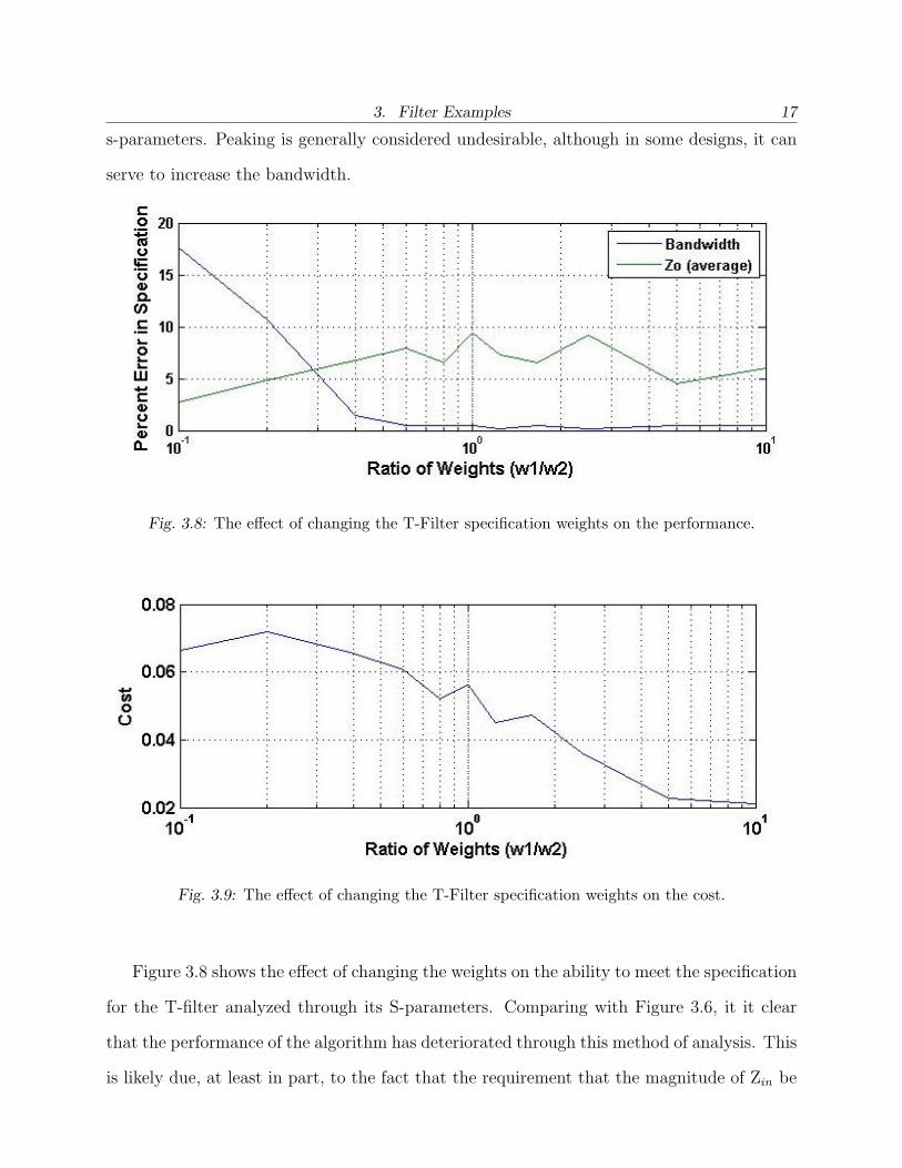
s-parameters. Peaking is generally considered undesirable, although in some designs, it can
serve to increase the bandwidth.
Fig. 3.8: The effect of changing the T-Filter specification weights on the performance.
Fig. 3.9: The effect of changing the T-Filter specification weights on the cost.
Figure 3.8 shows the effect of changing the weights on the ability to meet the specification
for the T-filter analyzed through its S-parameters. Comparing with Figure 3.6, it it clear
that the performance of the algorithm has deteriorated through this method of analysis. This
is likely due, at least in part, to the fact that the requirement that the magnitude of Zin be

3. Filter Examples 18
driven to 50Ω is an artificial one, created by the designer to approximate a good broadband
match. From this example, it is also evident that the designer requires a fair amount of
knowledge and intuition in order to get the genetic algorithm to produce a desirable result.
Finally, Figure 3.10 compares the frequency responses of the filters designed by the GA
using Equation-Based analysis and S-parameter analysis. It is clear that the algorithm was
able to design the filter very close to specification.
a) Filter Designed by Equation-Based Analysis b) Filter Designed by S-parameter Analysis
Fig. 3.10: S-parameter plots for the T-filters designed by the genetic algorithm.
3.3 Higher-Order Filter Design
Fig. 3.11: Three-stage low-pass filter.
A more complex filter design will now be attempted. The example is taken from [5], and
calls for the design of a maximally flat filter with a bandwidth of 2GHz, and a loss of at

3. Filter Examples 19
Cutoff Frequency (f−3db) 2 GHzLoss at 3 GHz 15dB
Zin,avg 50
Tab. 3.3: Design specifications for the 5th order filter design.
Example Population Generations Inductance Capacitance S11 Spec Number of Stages1 1400 9 (10pH,10nH) (10fF,10pF) None 32 700 10 (10pH,10nH) (10fF,10pF) None 33 1400 6 (1pH,10nH) (1fF,10pF) None 34 1400 9 (1pH,10nH) (1fF,10pF) None 35 3500 14 (1pH,10nH) (1fF,10pF) -10dB 3
Tab. 3.4: Example setups for the design of the low-pass filter.
least 15dB at 3GHz. Note that, unlike the reference solution provide in [5], the solutions
produced by the GA will not be maximally flat. In this design, we assume that we know
that the number of elements needed is 5, and so three L-C filter stages are used, as shown
in Figure 3.11. Inductance L1 is set to zero. Also, all specifications will be weighted equally
for the remainder of the experiments. In both of the previous examples, this was shown to
yield genomes that meet the specification well.
The genome for this analysis is composed of the 3 inductances and 3 capacitances in the
filter. The design specifications applicable to the cost function are given in Table 3.3.
3.3.1 Experiment
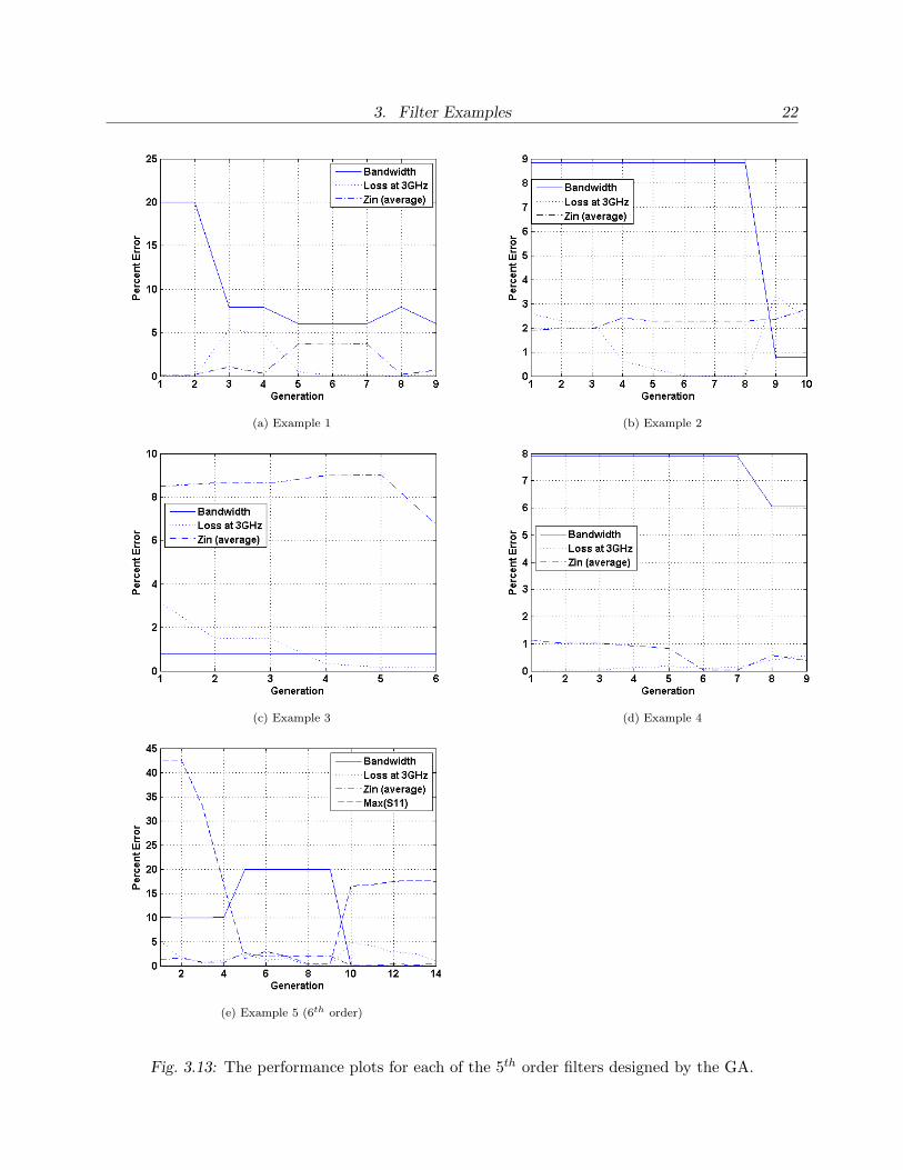
The performance of the algorithm will be explored through 5 experiments. The setup is
summarized in Table 3.4.
Examples 1 and 2 are almost the same in the their setup, aside from the size of the
population. Both setups were allowed to mutate for approximately the same number of
generations, at which point the final percent errors are quite comparable. From Figure 3.12
and Figures 3.13a,b, it appears as though the larger population size of Example 1 causes its
cost and specification percent errors to fall more quickly in early generations.

3. Filter Examples 20
In Examples 3 and 4, the size of the design space was increased by an order of magnitude
for each of the genes. This investigation is important, as it is questionable how accurately
a designer should be able to estimate the range of values. Figures 3.12 and 3.13c,d show
similar trends for the two experiments, even though Example 4 was allowed to mutate for
more generations. It is encouraging that the algorithm seems to be relatively insensitive
to this first investigation on increasing the range of allowable values, however future work
should characterize this effect in much greater detail.
Fig. 3.12: The figure shows the effect of the generation on the cost function of the algorithm.
As discussed in Section 3.2, the broadband input match is achieved by driving the magni-
tude of the average input impedance to 50Ω. Example 5 introduces the additional constraint
that the largest value of S11 over the band be limited to -10dB. In order to accomodate
this, inductance L1 was given the same range of values as the other inductance-genes. Fig-
ure 3.13e shows that although the percent errors of the initial population are far worse than
in the previous generations, 3 of the 4 specifications are able to be met quite well by the 5th
generation. After this time, the percent error of the worst specification continues to improve.

3. Filter Examples 21
Example L1 C1 L2 C2 L3 C31 0 1.4813 pF 0.4000 nH 81.3751 fF 5.5682 nH 3.2878 pF2 0 2.7729 pF 7.1569 nH 2.2128 pF 2.5596 nH 0.3165 pF3 0 2.2498 pF 1.1104 nH 0.8425 pF 5.7895 nH 2.5499 pF4 0 0.3886 pF 3.5971 nH 1.8243 pF 6.0627 nH 3.2958pF5 2.2246 pF 0.7492 pF 4.5295 nH 2.6218 pF 5.4467 nH 2.5102 pF
Tab. 3.5: Final design values for each of the higher-order filter examples.
Figure 3.12 shows that the cost for this example falls more steeply than any of the others.
Figure 3.14 shows the higher order effects that have been mutated into the model to help
keep S11 below -10dB over the band. Note that these effects are not nearly as pronounced
in any of the other examples.
The final inductance and capacitance values for the filter are summarized in Table 3.5.
Although the setup for each of the above experiments was different, there do appear to be
trends in the results that are common to all of them. From Figure 3.13, it seems that by
starting with such a large initial population, the algorithm will always be able to find a group
of models that is able to meet all but one or two of the requirements quite well within the
first generation. Through mutation and inheritance, the algorithm then attempts to meet
the remaining specifications. This may be advantageous for the designer, because it means
that very early on, a reasonable solution to the problem will emerge. It is only when all
specifications must be met that the designer would need to wait for many generations.
3. Filter Examples 22
(a) Example 1 (b) Example 2
(c) Example 3 (d) Example 4
(e) Example 5 (6th order)
Fig. 3.13: The performance plots for each of the 5th order filters designed by the GA.

3. Filter Examples 23
(a) Example 1 (b) Example 2
(c) Example 3 (d) Example 4
(e) Example 5 (6th order)
Fig. 3.14: The S-parameter plots for each of the 5th order filters designed by the GA.

4. GENETIC ALGORITHM FOR DISTRIBUTED AMPLIFIER DESIGN
Having demonstrated that the GA is able to design not only simple 2-3 element circuits,
but also more complex 5th– and 6th–order filters, the design of a distributed amplifier was
attempted. The distributed amplifier used in this work is similar to the one depicted in
Figure 1.3, except that instead of transmission lines connecting the two stages, lumped
inductances and capacitances are used. The exact model used is shown in Figure 4.1 and is
based on the model presented in [6].
Some modifications have been made in the interest of simplicity. For example, the parallel
capacitors in each of the gate and drain networks are not combined, for symmetry. Although
beyond the scope of this work, these capacitors can also be thought to include the parasitic
capacitances from the transistors. The transistor itself is modelled as an ideal voltage-
controlled current source (VCCS), with the current being drawn from the network at the
drain of the transistor. The transistors are implemented in a common-source configuration.
The motivation behind the examples in Chapter 3 was to show that the GA is able to
effectively analyze 2-port networks through ABCD matrices and S-parameter analysis. While
the distrubuted amplifier shown appears to be a 4-port network, by adding termination
impedances RD1 and RGN (Figure 1.3), the amplifier effectively becomes a 2-port network.
This derivation is provided in Appendix D.
With a 2-port network, we can set up the design specifications and let the GA perform
the optimization. For simplicity, we set the number of stages equal to two. The genome for
this experiment is then given by
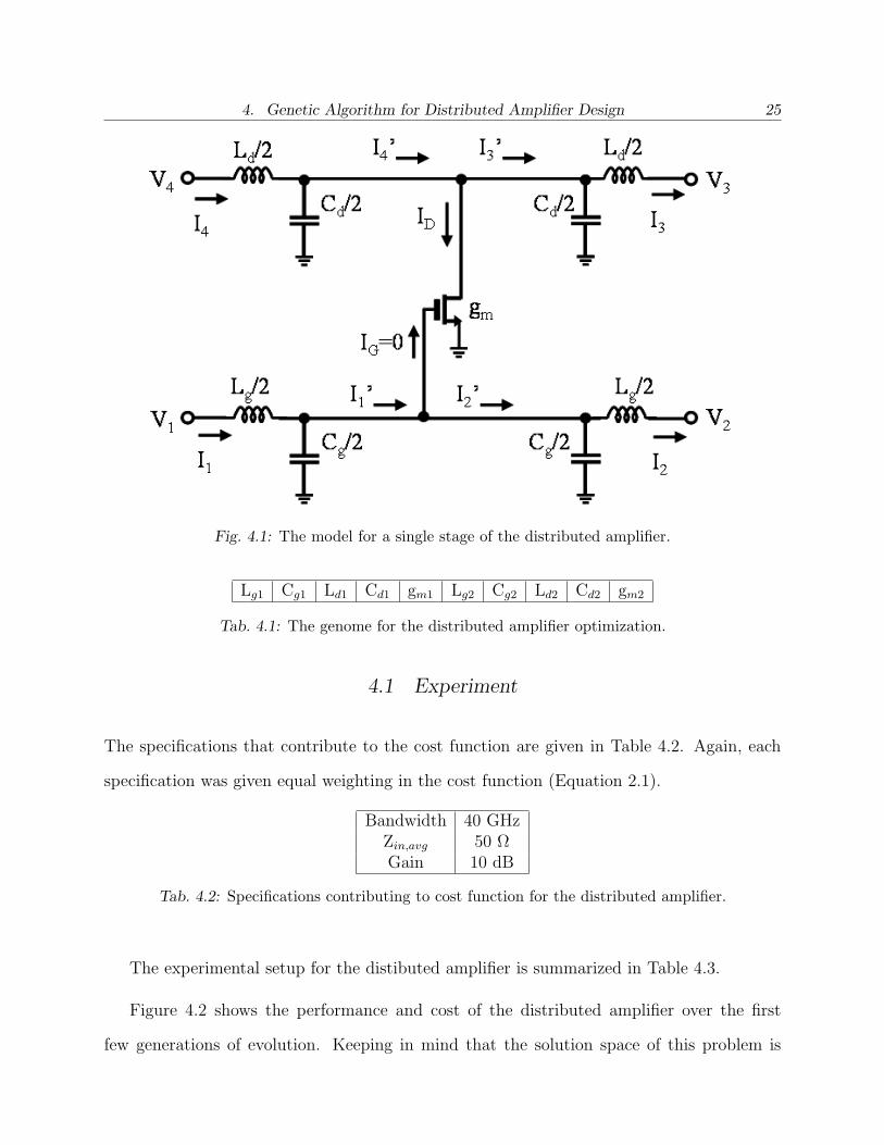
4. Genetic Algorithm for Distributed Amplifier Design 25
Fig. 4.1: The model for a single stage of the distributed amplifier.
Lg1 Cg1 Ld1 Cd1 gm1 Lg2 Cg2 Ld2 Cd2 gm2
Tab. 4.1: The genome for the distributed amplifier optimization.
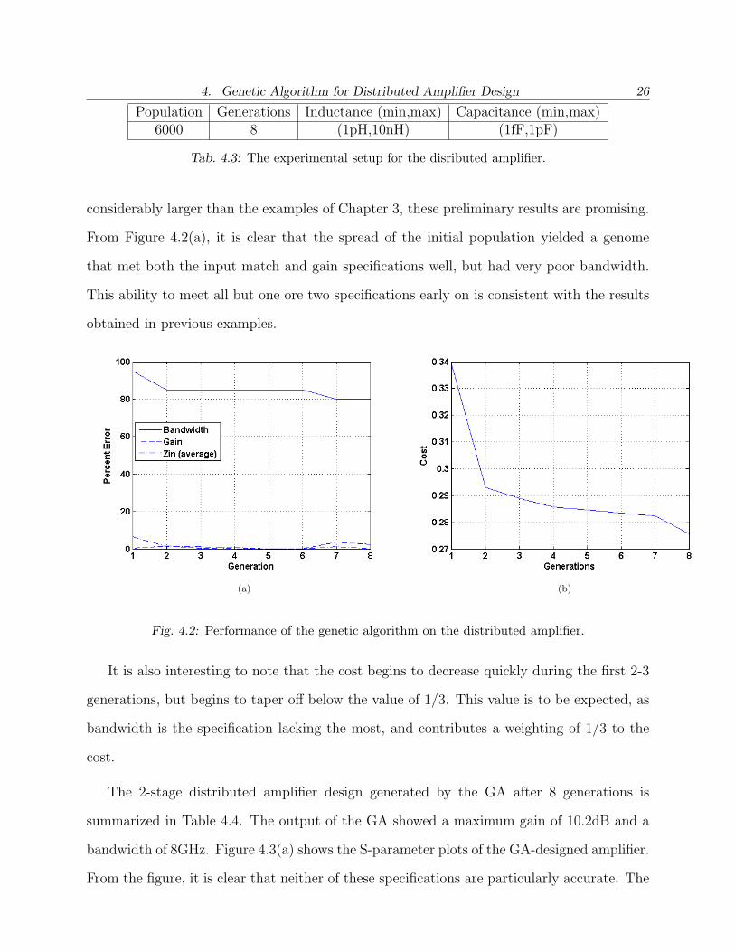
4.1 Experiment
The specifications that contribute to the cost function are given in Table 4.2. Again, each
specification was given equal weighting in the cost function (Equation 2.1).
Bandwidth 40 GHzZin,avg 50 ΩGain 10 dB
Tab. 4.2: Specifications contributing to cost function for the distributed amplifier.
The experimental setup for the distibuted amplifier is summarized in Table 4.3.
Figure 4.2 shows the performance and cost of the distributed amplifier over the first
few generations of evolution. Keeping in mind that the solution space of this problem is
4. Genetic Algorithm for Distributed Amplifier Design 26
Population Generations Inductance (min,max) Capacitance (min,max)6000 8 (1pH,10nH) (1fF,1pF)
Tab. 4.3: The experimental setup for the disributed amplifier.
considerably larger than the examples of Chapter 3, these preliminary results are promising.
From Figure 4.2(a), it is clear that the spread of the initial population yielded a genome
that met both the input match and gain specifications well, but had very poor bandwidth.
This ability to meet all but one ore two specifications early on is consistent with the results
obtained in previous examples.
(a) (b)
Fig. 4.2: Performance of the genetic algorithm on the distributed amplifier.
It is also interesting to note that the cost begins to decrease quickly during the first 2-3
generations, but begins to taper off below the value of 1/3. This value is to be expected, as
bandwidth is the specification lacking the most, and contributes a weighting of 1/3 to the
cost.
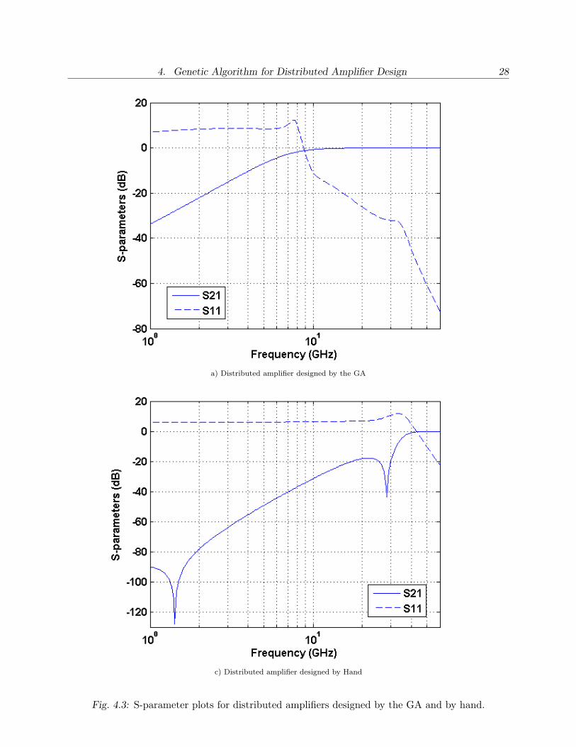
The 2-stage distributed amplifier design generated by the GA after 8 generations is
summarized in Table 4.4. The output of the GA showed a maximum gain of 10.2dB and a
bandwidth of 8GHz. Figure 4.3(a) shows the S-parameter plots of the GA-designed amplifier.
From the figure, it is clear that neither of these specifications are particularly accurate. The

4. Genetic Algorithm for Distributed Amplifier Design 27
Lg1 458.1 pHCg1 397.7 fFLd1 6.81 pHCd1 119.5 fFgm1 34.2 mA/VLg2 655.0 pHCg2 25.35 fFLd2 395.9 pHCd2 335.6 fFgm2 10.2 mA/V
Tab. 4.4: The distributed amplifier genome after 8 generations of evolution.
reason for this is that the number of data points used by the algorithm in its S-parameter
plots was limited to a much smaller number than that used to create Figure 4.3. This was a
design choice that had to be made in order keep the simulation time of the algorithm within
a reasonable time-frame. The result of this tradeoff was a design that suffers from peaking.
To compare, Figure 4.3 shows the S-parameter results for an amplifier designed by hand.
The design is outlined in Appendix E, and is only intended as a quick comparison. It is clear
that, although the human design also suffers from peaking, the it is likely that a design that
meets the specifications reasonably well could be obtained with only minor adjustment. The
use of a GA for the design of this 2-stage amplifier is then not easily justified.
4. Genetic Algorithm for Distributed Amplifier Design 28
a) Distributed amplifier designed by the GA
c) Distributed amplifier designed by Hand
Fig. 4.3: S-parameter plots for distributed amplifiers designed by the GA and by hand.
5. CONCLUSION
A genetic algorithm for the design of passive filters and a distributed amplifier was presented.
Through the cost function, the algorithm was demonstrated to drive the best models of
the population to meet the required specification. The algorithm successfully designed the
passive filters and resistor divider, and preliminary results from the algorithm’s distributed
amplifier design show promise for future work.
The main problem found in this work was that in order for the algorithm to yield a useful
solution, a substantially large amount of knowledge, experience, and intuition is required on
the part of the designer in setting the cost specifications. This is perfectly exemplified in the
design of the T-filter, where the input match specification needed to be changed several times.
As a result, the algorithm, as presented, is useful only to an intermediate-level designer—one
that does not have enough experience to design a circuit using more conventional, analytical
means, but also one with enough intuition to troubleshoot specification definitions in order
to achieve the desired result.
5.1 Future Work
Through the results of this first investigation, a substantial potential is seen for future work.
The main areas of improvement lie in three main areas: the algorithm, the circuit models,
and the implementatoin.
Future work for the GA itself includes implementation of more advanced forms of evolu-
tion, such as crossover and gradient descent. A more quantitative study of the performance
5. Conclusion 30
characteristics is also necessary. In particular, more work needs to be done on determining
how small an initial population the design can start with, and still converge to an optimal
solution within a reasonable number of generations. Different cost and mutation functions
should also be experimented with.
The circuit models themselves can also be improved by, for example, explicitly accounting
for the parasitics of both the transistors and the lumped components. This step is crucial if
the algorithm is ever to be used in either academia or industry for serious circuit design.
The implementation of the algorithm can be improved. In [2], hard-ware based genome
testing significantly sped up the optimization time. A more viable option for this work is
porting the algorithm to a faster programming language such as C. This would aid in both
design and development time.

APPENDIX

A. ABCD MATRICES
Fig. A.1: The ABCD matrix of a 2-Port Netork
One method of characterizing a 2-Port Network (Figure A.1) is through the network’s
ABCD matrix, which relates the voltages and currents of the two ports. The relationship is
given by:
V1
I1
=
A B
C D
V2
I2
(A.1)
The benefit of this method is that the ABCD matrix of a cascade of networks is given by
the product of the ABCD matrices of each of the individual networks, multiplied in order.
The S-parameters of the network, which relate incident and reflected voltage waves, can
also be easily calculated for a given characteristic impediance Zo using:
S11 =A + B/Zo − CZo −D
A + B/Zo + CZo + D(A.2)

A. ABCD Matrices 33
S12 =2(AD −BC)
A + B/Zo + CZo + D(A.3)
S11 =2
A + B/Zo + CZo + D(A.4)
S11 =−A + B/Zo − CZo + D
A + B/Zo + CZo + D(A.5)

B. T-MODEL ANALYSIS
The ABCD-matrix for the T-Filter is derived from the T-equivalent circuit of a 2-Port
network, shown in Figure B.1.
Fig. B.1: The T-equivalent Model of a 2-Port Network
From Figure 3.5, it is clear that for the T-Filter,
Z1 = jωL
2(B.1)
Z2 = jωL
2(B.2)
Z3 =1
jωC(B.3)

B. T-Model Analysis 35
From [5], the ABCD matrices for the T-equivalent model are given by:
A = 1 +Z1
Z3
(B.4)
B = Z1 + Z2 +Z1Z2
Z3
(B.5)
C =1
Z3
(B.6)
D = 1 +Z2
Z3
(B.7)
and so the ABCD matrix for the T-Filter is given by:
AT−Filter = 1− ω2LC
2(B.8)
BT−Filter = jωL− jω3L2C
4(B.9)
CT−Filter = jωC (B.10)
DT−Filter = 1− ω2LC
2(B.11)
From these ABCD values, the S-parameters can be derived using Equations A.2- A.5.
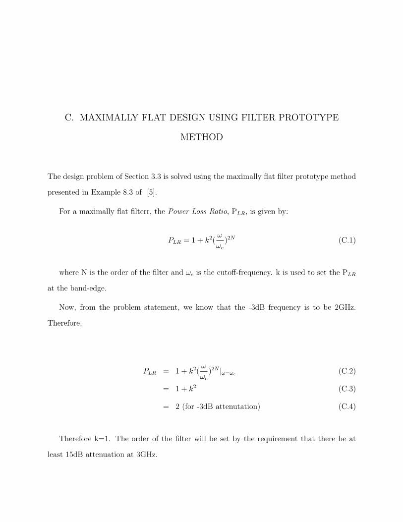
C. MAXIMALLY FLAT DESIGN USING FILTER PROTOTYPE
METHOD
The design problem of Section 3.3 is solved using the maximally flat filter prototype method
presented in Example 8.3 of [5].
For a maximally flat filterr, the Power Loss Ratio, PLR, is given by:
PLR = 1 + k2(ω
ωc
)2N (C.1)
where N is the order of the filter and ωc is the cutoff-frequency. k is used to set the PLR
at the band-edge.
Now, from the problem statement, we know that the -3dB frequency is to be 2GHz.
Therefore,
PLR = 1 + k2(ω
ωc
)2N |ω=ωc (C.2)
= 1 + k2 (C.3)
= 2 (for -3dB attenutation) (C.4)
Therefore k=1. The order of the filter will be set by the requirement that there be at
least 15dB attenuation at 3GHz.

C. Maximally Flat Design Using Filter Prototype Method 37
C1 0.984 pFL2 6.438 nHC2 3.183 pFL3 6.438 nHC3 0.984 pF
Tab. C.1: Inductances and capacitances satisfying the maximally-flat specification.
15 ≤ 10log(PLR) (C.5)
= 10log(1 + (f
fc
)2N)|f=3GHz (C.6)
Solving for N we find that N must be greater than 4.22, so the minimum order of the
filter is N=5. The element values for the maximally-flat prototype are obtained by looking
up Table 8.3 from [5], and are given in Table C.1.
D. DISTRIBUTED AMPLIFIER S-PARAMETER DERIVATION
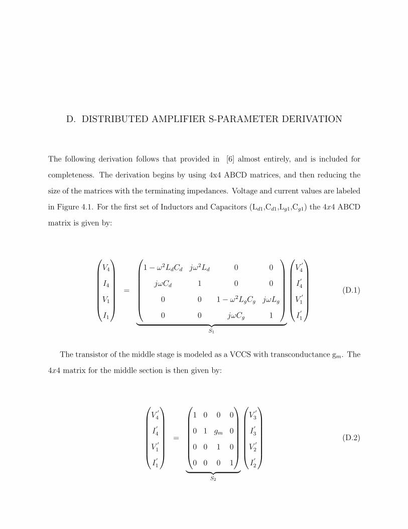
The following derivation follows that provided in [6] almost entirely, and is included for
completeness. The derivation begins by using 4x4 ABCD matrices, and then reducing the
size of the matrices with the terminating impedances. Voltage and current values are labeled
in Figure 4.1. For the first set of Inductors and Capacitors (Ld1,Cd1,Lg1,Cg1) the 4x4 ABCD
matrix is given by:
V4
I4
V1
I1
=
1− ω2LdCd jω2Ld 0 0
jωCd 1 0 0
0 0 1− ω2LgCg jωLg
0 0 jωCg 1
︸ ︷︷ ︸
S1
V′4
I′4
V′1
I′1
(D.1)
The transistor of the middle stage is modeled as a VCCS with transconductance gm. The
4x4 matrix for the middle section is then given by:
V′4
I′4
V′1
I′1
=
1 0 0 0
0 1 gm 0
0 0 1 0
0 0 0 1
︸ ︷︷ ︸
S2
V′3
I′3
V′2
I′2
(D.2)
D. Distributed Amplifier S-parameter Derivation 39
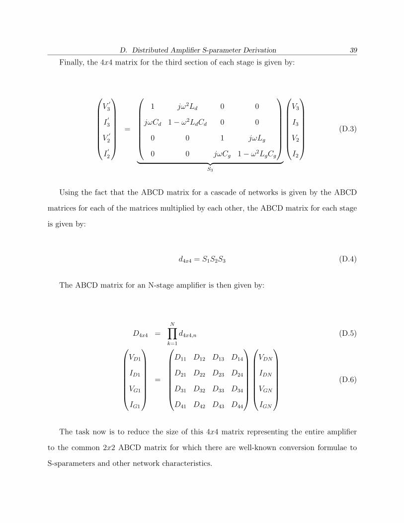
Finally, the 4x4 matrix for the third section of each stage is given by:
V′3
I′3
V′2
I′2
=
1 jω2Ld 0 0
jωCd 1− ω2LdCd 0 0
0 0 1 jωLg
0 0 jωCg 1− ω2LgCg
︸ ︷︷ ︸
S3
V3
I3
V2
I2
(D.3)
Using the fact that the ABCD matrix for a cascade of networks is given by the ABCD
matrices for each of the matrices multiplied by each other, the ABCD matrix for each stage
is given by:
d4x4 = S1S2S3 (D.4)
The ABCD matrix for an N-stage amplifier is then given by:
D4x4 =N∏
k=1
d4x4,n (D.5)
VD1
ID1
VG1
IG1
=
D11 D12 D13 D14
D21 D22 D23 D24
D31 D32 D33 D34
D41 D42 D43 D44
VDN
IDN
VGN
IGN
(D.6)
The task now is to reduce the size of this 4x4 matrix representing the entire amplifier
to the common 2x2 ABCD matrix for which there are well-known conversion formulae to
S-sparameters and other network characteristics.

D. Distributed Amplifier S-parameter Derivation 40
We begin by adding the terminating impedances to the first stage of the drain line, and
the N th stage of the gate line. The relationships that result are:
ID1 = − VD1
RD1
(D.7)
IGN =VGN
RGN
(D.8)
D can be reduced to a 3x4 matrix by dividing the first row by RD1 and adding it to the
second. It can be further reduced by dividing the fourth column by RGN and adding it to
the third column. These operations yield:
0
VG1
IG1
=
D21 + D11
RD1D12 + D12
RD1D13 + D13
RD1+ D24
RGN+ D14
RGNRD1
D31 D32 D33 + D34
RGN
D41 D42 D43 + D44
RGN
VDN
IDN
VGN
(D.9)
Hand analysis can then be used in the first line to represent VGN as a function of VDN
and IDN . The ABCD matrix for the distributed amplifier is then given by:
VG1
IG1
=
D31 −
(D21+D11RD1
)(D33+D34RG1
)
D23+D13RD1
+D24+
D14RD1
RGN
D32 −(D22+
D12RD1
)(D33+D34RG1
)
D23+D13RD1
+D24+
D14RD1
RGN
D41 −(D21+
D11RD1
)(D43+D44RG1
)
D23+D13RD1
+D24+
D14RD1
RGN
D42 −(D22+
D12RD1
)(D33+D34RG1
)
D23+D13RD1
+D24+
D14RD1
RGN
VDN
IDN
(D.10)
The S-parameters of the amplifier can then be determined using Formulae A.2- A.5.
E. HAND DESIGN OF A DISTRIBUTED AMPLIFIER
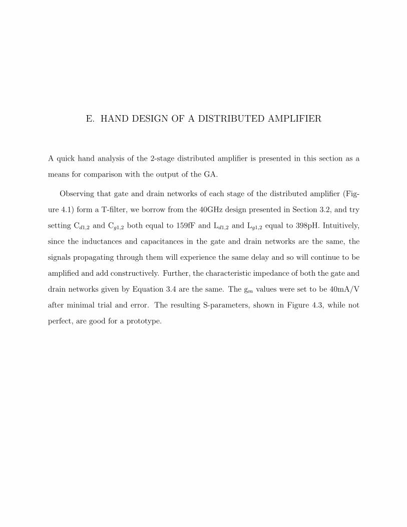
A quick hand analysis of the 2-stage distributed amplifier is presented in this section as a
means for comparison with the output of the GA.
Observing that gate and drain networks of each stage of the distributed amplifier (Fig-
ure 4.1) form a T-filter, we borrow from the 40GHz design presented in Section 3.2, and try
setting Cd1,2 and Cg1,2 both equal to 159fF and Ld1,2 and Lg1,2 equal to 398pH. Intuitively,
since the inductances and capacitances in the gate and drain networks are the same, the
signals propagating through them will experience the same delay and so will continue to be
amplified and add constructively. Further, the characteristic impedance of both the gate and
drain networks given by Equation 3.4 are the same. The gm values were set to be 40mA/V
after minimal trial and error. The resulting S-parameters, shown in Figure 4.3, while not
perfect, are good for a prototype.
BIBLIOGRAPHY
[1] IEEE Antenna and Propagation Society International Symposium and USNC/URSI Na-
tional Radio Science Meeting, Evolutionary Design of an X-Band Antenna for NASA’s
Space Technology 5 Mission, vol. 3, 2004.
[2] NASA/DoD Conference of Evolution Hardware, An Evolvable Antenna Platform Based
on Reconfigurable Reflectarrays, 2005.
[3] S. Haykin and M. Moher, Introduction to Analog & Digital Communications, Second
Edition. John Wiley & Sons, Inc., 2007.
[4] D. Shaeffer and T. Lee, “A 1.5-v, 1.5-ghz cmos low noise amplifier,” IEEE Journal of
Solid-State Circuits, vol. 32, pp. 745–759, May 1997.
[5] D. M. Pozar, Microwave Engineering, 3rd Ed. John Wiley & Sons, Inc., 2005.
[6] K. K. Moez, Design of CMOS Distributed Amplifiers for Broadband and Wireless Com-
munication Applications. PhD thesis, University of Waterloo, 2006.