a low-cost unified experimental fpga board for cryptography
TRANSCRIPT

A Low-Cost Unified Experimental FPGA Boardfor Cryptography Applications
Matej Bartık, Jirı Bucek
Czech Technical University in Prague, Faculty of Information Technology{matej.bartik; jiri.bucek}@fit.cvut.cz
Abstract—This paper describes the evaluation of availableexperimental boards, the comparison of their supported setof experiments and other aspects. The second part of thisevaluation is focused on the design process of the PCB (PrintedCircuit Board) for an FPGA (Field Programmable Gate Array)based cryptography environment suitable for evaluating the latesttrends in the IC (Integrated Circuit) security like Side–ChannelAttacks (SCA) or Physically Unclonable Function (PUF). Itleads to many criteria affecting the design process and also thesuitability for evaluating and measuring results of the attacks andtheir countermeasures. The developed system should be open,versatile and unrestricted by the U.S. law [1].
I. INTRODUCTION
Security issues (cryptanalysis and side-channel attacks) aregetting more and more important during last years. Nowadays,current research on hardware security is focused on twomethods: how to decrease vulnerability of integrated circuitsto leak their secrets and how to devise methods of secureauthentication. For example, the Differential Power Analysis(DPA) is probably the most efficient way to retrieve secretsfrom ICs, and practically all security devices must includesome form of countermeasures. The representative example ofauthentication (and also key generation) is PUF, the securityof which is widely discussed and attacks and countermeasuresare developed.
The progress of these technologies requires to teach fu-ture hardware security engineers how to evaluate attacksand countermeasures against attacks. Laboratory courses re-quire [2] huge amount of (expensive) experimental boards likeSASEBO [4] or Evariste [5] project. PUF related researchrequires the same or higher number of experimental boards.Both of the goals require to design and create a low costdevelopment board equipped with a state of the art FPGA. Theboard design process should reflect the needs of cryptographicexperiments and applications.
II. SUPPORTED EXPERIMENTS
In the following subsections, we will summarize the in-tended experimental application fields of the developmentboard.
A. Power Analysis Attacks
Every digital circuit leaks some internal information viaits power consumption. Paul Kocher et al. [6] showed that bypower consumption measuring during cryptographic operationsand by analyzing these measurements, the secret key can be
discovered, even though the cipher is otherwise (mathemat-ically) secure. In order to experiment with power analysisattacks, a current measuring device (usually a resistor) is addedto a supply rail in order to measure the current consumption.
The power consumption is measured as a sequence of sam-ples in time (a power trace) using a digital oscilloscope (seeFig. 1), and the power traces are then transferred to a computerfor analysis. There are several methods for analyzing the powertraces. Simple power analysis (SPA) use a single power traceto directly discover the secret key.
Fig. 1. The power trace example of the AES cipher [2].
Differential power analysis (DPA) uses multiple powertraces, each is measured for the encryption with different(known) data [7]. The secret key is then derived part bypart using statistical methods (testing of hypotheses about thevalues of the sub-keys). For each sub-key, all possible valuesare analyzed, a hypothetical power consumption is computedusing the known data and a power model, and the correct oneis found by correlating the hypothetical consumption with themeasured consumption across all traces for some point in time.
B. Physically Unclonable Function (PUF)
The PUF [8] [9] is a challenge–response mechanism thatuses physical properties of integrated circuits (deviations in themanufacturing process like unique delay of the logic circuitspaths in the each IC) to create a unique response that identifiesthe IC conclusively. The fundamental principle of PUF isshown in Fig. 2. The response can be used as a secret keyfor the cryptography or memoryless key storage.

Fig. 2. The principle of the PUF with different responses (Rx) [9].
C. Cipher Implementation
An FPGA is a perfect tool for implementing of any cipher,for example the AES (Advanced Encryption Standard) cipher(that can be attacked by the DPA method). Modern FPGAs areusing a hardcoded AES cipher block as a protection againstcopying the FPGA bitstream [20]. We can also apply theDPA [11] technique to attack the FPGA configuration andbitstream loading block to retrieve the secret key for thebitstream decryption.
D. FPGA Configuration and AES Decryption of the Bitstream
A modern FPGAs can use an AES cipher as a protectionagainst copying the FPGA bitstream [20]. We can also applythe DPA [11] technique to attack the FPGA configurationand bitstream loading block to retrieve the secret key for thebitstream decryption.
E. SHA-1 Challenge – Response Authentication
The SHA–1 EEPROMs like Maxim Integrated DS2432is predecessor (see Fig. 3) of the PUF technology used fora bitstream authentication [21]. This SHA–1 EEPROM can bealso attacked like the PUF.
Fig. 3. The principle of the SHA-1 challenge – response authentication. [21]
F. Evaluating Quality of the TRNG
Random number generation is of critical importancefor many cryptographic methods and applications, such askey generation, digital signature computation, and challenge-response authentication. True random number generators(TRNGs) rely on physical noise sources such as thermal noise,phase jitter or metastability, from which they extract entropyto produce a random bitstream. Some methods are suitable forimplementation in FPGAs, such as ring-oscillator based TRNG[3].
III. AVAILABLE COMPETING PLATFORMS
In this section a brief comparison will be presented betweenthree similar projects (SASEBO [4], Evariste [5] and FO-BOS [15]) focused on the creation of the unified environmentfor testing, evaluating a measuring systems implementingcryptographic hardware.
A. SASEBO
SASEBO [4] is the most complex project focused onthe cryptography providing a complete toolset of boards (seeTable I.), software and measuring equipment. There are sevendifferent SASEBO boards differing by the used chip (ASICor FPGA). The most of SASEBO boards (see Fig. 5) containsone FPGA for interfacing PC over the USB port (trough adedicated chip) and control the dedicated ASIC/FPGA (up toXilinx Kintex-7) for cryptography purpose (a control – victimschema is used, see Fig. 4).
TABLE I. COMPARISON OF THE SASEBO BOARDS [22]
Board Vendor Control Victim YearSASEBO Xilinx XC2VP30 XC2VP7 2007SASEBO–G Xilinx XC2VP30 XC2VP7 2008SASEBO–GII Xilinx XC3S400A XC5VLX30 or LX50 2009SASEBO–GIII Xilinx XC6SLX45 XC7K325T 2013SASEBO–B Altera EP2S30F672C5N EP2S15F484C5N 2008SASEBO–R ASIC XC2VP30 LSI 130nm process 2008SASEBO–W Xilinx XC6SLX150 Smart Card socket 2012
Fig. 4. The control – victim block diagram
Control & cryptographic parts have separate power suppliesto limit the interference between them, but interference canspread over the common ground. The cryptographic chipusually has no decoupling capacitors (or a few positions formounting capacitors, but the number of positions is signif-icantly lower than the amount recommended by the chipvendor) reducing the average number of required measure-ments for the DPA [12]. The biggest disadvantage of theSASEBO boards are their price (approximately 1500$–2000$)that prevent to equip each student with his own board. Fur-ther disadvantages are lack of decoupling capacitors that aremounted on commercial FPGA boards according to FPGAvendor datasheet (we can’t simulate the real operating con-ditions for the PUF).
B. Evariste II and Evariste III
The Evariste II project [5] is focused primarily on fairbenchmarking of true random number generators, but can alsobe used for other purposes (see Fig. 6). There are 9 differentboards with different FPGA chips using the motherboard foracquiring measured data. These boards have the same generalfeatures like using linear low–noise power regulators to supplyvoltage for the FPGA (Core, Auxiliary, I/O). Like in the

Fig. 5. The SASEBO–GIII board. [13].
SASEBO, the communication and data acquisition is providedby the USB interface (Cypress FX2 – CY7C68013A), butthere is no control FPGA. The control and the interface partis implemented in the measured FPGA. There is no isolationfrom the communication IC (FX2) to prevent the interference.Currently supported boards are in Table II.
Fig. 6. Setup of the Evariste II project. [14]
TABLE II. COMPARISON OF THE EVARISTE II AND III BOARDS [14]
Evariste II ModulesBoard Vendor ChipCyclone III FPGA module v2.2 Altera EP3C25F256-C8Cyclone III FPGA module v2.4 Altera EP3C25F256-C8Arria II FPGA module v 1.0 Altera EP2AGX45CU17C6Spartan 3 FPGA module v 2.1 Xilinx XC3S700ANVirtex 5 FPGA module v 1.0b Xilinx XC5VLX30TFusion FPGA module v 2.0 Microsemi M7AFS600 FGG256X2
Evariste III ModulesBoard Vendor ChipSpartan 6 FPGA module v 1.0 Xilinx XC6FLX16Cyclone V FPGA module v.CyV2 Altera 5CEBA4F17C8NSmartFusion2 FPGA module v.1 Microsemi M2S025FGG484
C. FOBOS
The idea of FOBOS project [15] is an attempt to createa unified environment for cryptographic purposes using ordi-nary FPGA development boards widely used for teaching. Alltwelve supported boards are in the university program of bothmajor FPGA vendors, Xilinx and Altera.
FOBOS shares the same idea of SASEBO (dual FPGAsystem control–victim), but each part is created from anindividual development board. The effort is focused on saving
money by using ordinary boards to create a low–cost system.In case that the university/laboratory doesn’t already have theseboards (see Table III.), the price for equipping students is high(cheaper half of these boards are discontinued, second half isexpensive). There is no isolation to prevent noise from thecontrol system.
TABLE III. COMPARISON OF THE FOBOS BOARDS. [15]
FOBOS Control BoardsBoard Chip PriceNexys–2 XC3S500E 149 $ (Discontinued)Nexys–3 XC6LX16 270 $
FOBOS Victim Board — Xilinx FPGA basedBoard Vendor ChipSpartan–3E Starter Kit XC3S500E 299 $ (Legacy)Spartan–3E - 1600 DB XC3S1600E 225 $ (Discontinued)Atlys XC6LX45 419 $ (Legacy)Genesys XC5VLX50T 899 $ (Legacy)ML605 XC6VLX240T 1995 $KC705 XC7K325T 1695 $
FOBOS Victim Board — Altera FPGA basedAltera DE1 Cyclone II 2C20 150 $Altera DE2-115 Cyclone IV EP4CE115 495 $Cyclone III Starter Cyclone III EP3C25F324 200 $Altera DE4 Stratix IV GX EP4SGX230 2995 $
IV. EXPERIMENTAL BOARD REQUIREMENTS
In this section we will discuss some requirements for thePCB to support all mentioned goals [16]. Requirements forone goal can be opposite for the another goal.
A. Simple / Differential Power Analysis (SPA/DPA)
The secret key is obtained by measuring the FPGA corepower consumption. From these measurements a power tracewaveform (representing voltage in the time) we will created,from which the secret key can be determined. Two mainSPA/DPA requirements must be met: ability to measure thecurrent for the FPGA core (using a shunt resistor) and removedecoupling capacitors for increasing current surges (voltagepeaks) that made the key recovery much easier (but notimpossible [17]). Additional requirements for attacking FPGAconfiguration block are: presence of a (Quad) SPI Flash chipas a bitstream storage and VBATT pin have to be connected outonto a pin header (FPGA key storage is a volatile memory).
B. Physically Unclonable Function (PUF)
The result of PUF circuit prototype can vary due todifferent operational conditions and other influences from theenvironment surrounding the measured board. Parameters thataffect measurements outside the board are the change of theoperating temperature and EMI (Electro Magnetic Interfer-ence) in the power supply source.
The most important parameter is the FPGA core voltage,that can not be simply modified on an ordinary board andshould meet the requirements of the FPGA chip vendor (toler-ance is typically 3%–5%). The core voltage of modern FPGAsis usually 1 V, so the variance can be maximally 100 mV peak–to–peak using a proper decoupling technique. A precise powersolution with a voltage control in the order of millivolts andability to change output voltage on–the–fly from the controlsystem is required. The solution should support a standardized
interconnection bus like an I2C or an SPI to support automatedmeasurements. The current required by a typical mid–rangeFPGA core is 3–4 amperes, thus limits the choice.
C. Cipher Implementation in the FPGA
Asymmetric ciphers and methods need mostly more FPGAresources than symmetric ones. The board (and FPGA foot-print and pinout) should be the same for all chips across theFPGA family. This allows to use smaller or bigger chips ondemand and modify the board price to reach expected budget.
D. General Requirement – EMC and Measurement Process
The general requirements also affect the final design ofthe board. The most common one is to comply with theEMC (Electro Magnetic Compatibility) requirements [18]. Themeasured values can be jammed by other circuits placed on theboard. For example, Cypress FX2 (CY7C68013A) is widelyused for communication between PC and FPGA via USB. Theinner architecture of FX2 includes the 8051 microcontroller.There is no way to be sure that the measured consumption (forSPA/DPA) is from the FPGA only. Even FX2 is not sharingpower supplies with the FPGA, a noise from I/O pins cancause a small interference in measured voltages.
This is an example based on our research [2] with Evaristeboards where the Cypress FX2 circuit is used. We are ableto retrieve the AES secret key no matter how the AES werecalculated because the power activity of the FX2 is higher thanthe power activity of the measured FPGA. To lower the systemnoise, optocouplers circuits should be used to divide the boardto an FPGA part and the interface part. The control will beprovided by a control application on PC.
V. CHARACTERISTICS OF THE EXPERIMENTAL BOARD
A. System Partitioning
The cost of the designed system can be reduced in differentways. The first idea is not to use the control–victim schemalike SASEBO or FOBOS. The price goes down by removingone FPGA chip (one development board), so we got inspiredby the Evariste project. The save of one FPGA will reducethe board size and might allow to use a lower count of PCBlayers.
B. FPGA
The majority of the mentioned boards from all projects arebased on the Xilinx Spartan-3E technology. On the other hand,there are only two boards equipped with a state of the art FPGAlike Xilinx Kintex-7. The final board should contain a modernFPGA. Xilinx provides a cheaper alternative to Kintex-7 calledArtix-7, based on same technology with similar features. Artix-7 FPGAs are available in many packages, but the FT256package is the only one that met the requirements (4 layerPCB, variety of available chips).
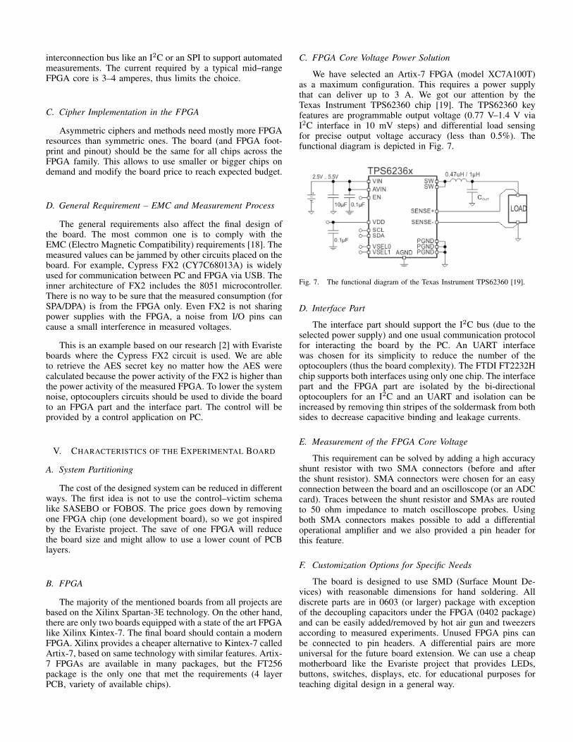
C. FPGA Core Voltage Power Solution
We have selected an Artix-7 FPGA (model XC7A100T)as a maximum configuration. This requires a power supplythat can deliver up to 3 A. We got our attention by theTexas Instrument TPS62360 chip [19]. The TPS62360 keyfeatures are programmable output voltage (0.77 V–1.4 V viaI2C interface in 10 mV steps) and differential load sensingfor precise output voltage accuracy (less than 0.5%). Thefunctional diagram is depicted in Fig. 7.
Fig. 7. The functional diagram of the Texas Instrument TPS62360 [19].
D. Interface Part
The interface part should support the I2C bus (due to theselected power supply) and one usual communication protocolfor interacting the board by the PC. An UART interfacewas chosen for its simplicity to reduce the number of theoptocouplers (thus the board complexity). The FTDI FT2232Hchip supports both interfaces using only one chip. The interfacepart and the FPGA part are isolated by the bi-directionaloptocouplers for an I2C and an UART and isolation can beincreased by removing thin stripes of the soldermask from bothsides to decrease capacitive binding and leakage currents.
E. Measurement of the FPGA Core Voltage
This requirement can be solved by adding a high accuracyshunt resistor with two SMA connectors (before and afterthe shunt resistor). SMA connectors were chosen for an easyconnection between the board and an oscilloscope (or an ADCcard). Traces between the shunt resistor and SMAs are routedto 50 ohm impedance to match oscilloscope probes. Usingboth SMA connectors makes possible to add a differentialoperational amplifier and we also provided a pin header forthis feature.
F. Customization Options for Specific Needs
The board is designed to use SMD (Surface Mount De-vices) with reasonable dimensions for hand soldering. Alldiscrete parts are in 0603 (or larger) package with exceptionof the decoupling capacitors under the FPGA (0402 package)and can be easily added/removed by hot air gun and tweezersaccording to measured experiments. Unused FPGA pins canbe connected to pin headers. A differential pairs are moreuniversal for the future board extension. We can use a cheapmotherboard like the Evariste project that provides LEDs,buttons, switches, displays, etc. for educational purposes forteaching digital design in a general way.

VI. PRICE CALCULATION OF THE EXPERIMENTAL BOARD
The experimental board is designed (see Fig. 8 and Fig. 9)for small batch production of 30 boards. The board outlineis the same as the smart card dimensions thus the area ofthe board is 7.17 square inch (46.25 cm2). The BGA (BallGrid Array) packages require an ENIG (Electroless NickelImmersion Gold) surface finishing. The board price is 11$including a stencil.
The components price depends on the used FPGA. For ourneeds the Artix-7 35T (XC7A35T-1FTG256C) is sufficient andthe cost is 25$ only. The price for all remaining componentsis 95$ and the cost of the assembly process is 34$ perboard. The cost of the assembled board is approximately 165$(respectively 200$ including VAT and other charges) that issignificantly below the price of competitor boards (SASEBO1500$, Evariste 500$, FOBOS 1000$) with the same or morefeatures supported. The total price will be even lower thanksto discounts (25%) for chips applied from 10–25 chips.
VII. CONCLUSION
We evaluated three different projects (SASEBO, Evariste,FOBOS) focused on measuring and evaluating cryptographicapplications in hardware (FPGA). We described their ad-vantages and disadvantages (the spread of the EMI to themeasured part because of no isolation between the controlpart and measured part) and we summarized a state of the art(requirements) for a new low–cost FPGA board (and effectsof these requirements).
The board has been designed to be versatile anduniversal for evaluating various cryptographic techniques(PUF, SPA, DPA, cipher implementation and others at-tacks/countermeasures) and is the only board supporting theSPA/DPA and the PUF evaluation at the same board. Theboard is fully operational and we delivered a state of the artFPGA (Xilinx Artix-7) equipped board to researchers, teachersand student regardless of low cost demands. The board isfurther easily customizable to extend the range of possibleexperiments with a basic soldering equipment.
ACKNOWLEDGMENT
This research has been partially supported by the projectSGS16/121/OHK3/1T/18 and by the grant GA16-05179S ofthe Czech Grant Agency, Fault-Tolerant and Attack-ResistantArchitectures Based on Programmable Devices: Research ofInterplay and Common Features (2016–2018).
REFERENCES
[1] SASEBO-G-II-32 Side-channel Attack Standard Evaluation Board, Dig-ilent Inc. [Online]. Available: http://store.digilentinc.com/sasebo-g-ii-32-side-channel-attack-standard-evaluation-board-by-inrevium-retired/
[2] Stepanek, F.; Bucek, J.; Novotny, M., ”Differential Power Analysis underConstrained Budget: Low Cost Education of Hackers,” in Digital SystemDesign (DSD), 2013 Euromicro Conference on, pp.645-648, 4-6 Sept.2013 doi: 10.1109/DSD.2013.130
[3] Buchovecka, S.; Lorencz, R.; Kodytek, F.; Bucek, J., ”True RandomNumber Generator based on ROPUF circuit”, in Digital System Design(DSD), 2016 Euromicro Conference on, pp.519-523, Aug. 31-Sept. 2,2016
Fig. 8. The developed PCB of new experimental board with an Artix–7FPGA and isolated communication interface part with only 4 layers.
Fig. 9. The developed and operational board with assembled components.

[4] Simion, E.; Burciu, P., ”A view to SASEBO project,” in Elec-tronics, Computers and Artificial Intelligence (ECAI), 2013 Inter-national Conference on , vol., no., pp.1-6, 27-29 June 2013 doi:10.1109/ECAI.2013.6636186
[5] Fischer, V.; Bernard, F.; Haddad, P., ”An open-source multi-FPGAmodular system for fair benchmarking of True Random Number Gen-erators,” in Field Programmable Logic and Applications (FPL), 201323rd International Conference on , vol., no., pp.1-4, 2-4 Sept. 2013 doi:10.1109/FPL.2013.6645570
[6] Kocher, P., Jaffe, J., Jun, B. Differential power analysis, In: Wiener, M.(ed.) CRYPTO 1999. LNCS, vol. 1666, pp. 388397. Springer, Heidelberg(1999)
[7] Benhadjyoussef, N.; Mestiri, H.; Machhout, M.; Tourki, R., ”Implementa-tion of CPA analysis against AES design on FPGA,” in Communicationsand Information Technology (ICCIT), 2012 International Conferenceon , vol., no., pp.124-128, 26-28 June 2012 doi: 10.1109/ICCITech-nol.2012.6285774
[8] PUF Physical Unclonable Functions, NXP [Online]. Available:www.nxp.com/documents/other/75017366.pdf
[9] Background on Physical Unclonable Functions (PUFs), Virginia Tech[Online]. Available: http://rijndael.ece.vt.edu/puf/background.html
[10] Developing Tamper Resistant Designs with Xilinx Virtex-6and 7 Series FPGAs (XAPP1084), Xilinx [Online]. Available:http://tinyurl.com/p32ez9f
[11] Sugawara, T.; Homma, N.; Aoki, T.; Satoh, A., ”Differential poweranalysis of AES ASIC implementations with various S-box circuits,”in Circuit Theory and Design, 2009. ECCTD 2009. European Confer-ence on , vol., no., pp.395-398, 23-27 Aug. 2009 doi: 10.1109/EC-CTD.2009.5275004
[12] DPA Characteristic Evaluation of SASEBO for Board Level Simu-lations, Toshihiro Katashita, Akashi Satoh, Katsuya Kikuchi, HiroshiNakagawa and Masahiro Aoyagi, First International Workshop on Con-structive Side-Channel Analysis and Secure Design 2010 (COSADE2010), Proceedings of COSEADE 2010, pp.36-39, February 2010.
[13] Hori, Y.; Katashita, T.; Sasaki, A.; Satoh, A., ”SASEBO-GIII: Ahardware security evaluation board equipped with a 28-nm FPGA,” inConsumer Electronics (GCCE), 2012 IEEE 1st Global Conference on ,vol., no., pp.657-660, 2-5 Oct. 2012 doi: 10.1109/GCCE.2012.6379944
[14] Hardware, Laboratoire Hubert Curien [Online]. Available: https://labh-curien.univ-st-etienne.fr/wiki-evariste/index.php/Hardware
[15] R. Velegalati and J.-P. Kaps, Towards a Flexible, Opensource BOard forSide-channel analysis (FOBOS), June, 2013, Cryptographic architecturesembedded in reconfigurable devices, CRYPTARCHI 2013
[16] Katashita, T.; Satoh, A.; Sugawara, T.; Homma, N.; Aoki, T., ”Develop-ment of side-channel attack standard evaluation environment,” in CircuitTheory and Design, 2009. ECCTD 2009. European Conference on , vol.,no., pp.403-408, 23-27 Aug. 2009 doi: 10.1109/ECCTD.2009.5275001
[17] Iokibe, K.; Amano, T.; Toyota, Y., ”On-board decoupling ofcryptographic FPGA to improve tolerance to side-channel attacks,”in Electromagnetic Compatibility (EMC), 2011 IEEE InternationalSymposium on , vol., no., pp.925-930, 14-19 Aug. 2011 doi:10.1109/ISEMC.2011.6038441
[18] Hubing, T., ”PCB EMC design guidelines: a brief annotated list,”in Electromagnetic Compatibility, 2003 IEEE International Sym-posium on , vol.1, no., pp.34-36 vol.1, 18-22 Aug. 2003 doi:10.1109/ISEMC.2003.1236559
[19] TPS62360 Datasheet, Texas Instruments [Online]. Available:http://www.ti.com/lit/gpn/tps62360
[20] Developing Tamper Resistant Designs with Xilinx Virtex-6and 7 Series FPGAs (XAPP1084), Xilinx [Online]. Available:http://tinyurl.com/p32ez9f
[21] FPGA IFF Copy Protection Using Dallas Semiconductor/MaximDS2432 Secure EEPROMs (XAPP780), Xilinx [Online]. Available:http://tinyurl.com/nglv9mf
[22] Side-channel attack standard evaluation board (SASEBO), http://www.morita-tech.co.jp/SASEBO/en/index.html, Morita Tech. Co., Ltd.SASEBO Web Site.