a low-noise frequency synthesizer for infrastructure ... · a low-noise frequency synthesizer for...
TRANSCRIPT

A Low-Noise Frequency Synthesizer for Infrastructure Applications
Shayan Farahvash, William Roberts, Jake Easter, Rachel Wei, Dave Stegmeir, Li Jin RFMD, USA

Outline
• Motivation
• Design Challenges
• VCO
• Capacitor Array
• Charge Pump
• Calibration
• Conclusion

Motivation
Why an integrated infrastructure-grade synthesizer?
• Semi-integrated solution with an external VCO is expensive• Recent wireless standards (e.g., WCDMA) have a lax
requirement on the phase noise compared to legacy ones (e.g., GSM)
• Power consumption requirements for infrastructure products are not as tight as those for handsets

Design Challenges
• Phase Noise
• Tuning Bandwidth
• Kv Variation
• Design Stability• Manufacturing variation• Process variation• Temperature
• Layout Constraints
• Current Consumption
Phase Noise
Stability
Kv
Bandwidth
Current

VCO
• Colpitts active core
• No tail current
• Linearization of the
tuning curve using C3
and C4
• Tuning sensitivity
adjustment using C1
and C2
• On-chip low-noise
regulator

Simulated VCO Performance
Similar to other Colpitts variations, there is an optimum n
87
7
65
5
CCC
CCCn

Simulated VCO Performance
Optimum n coincides with voltage-limited operation
87
7
65
5
CCC
CCCn
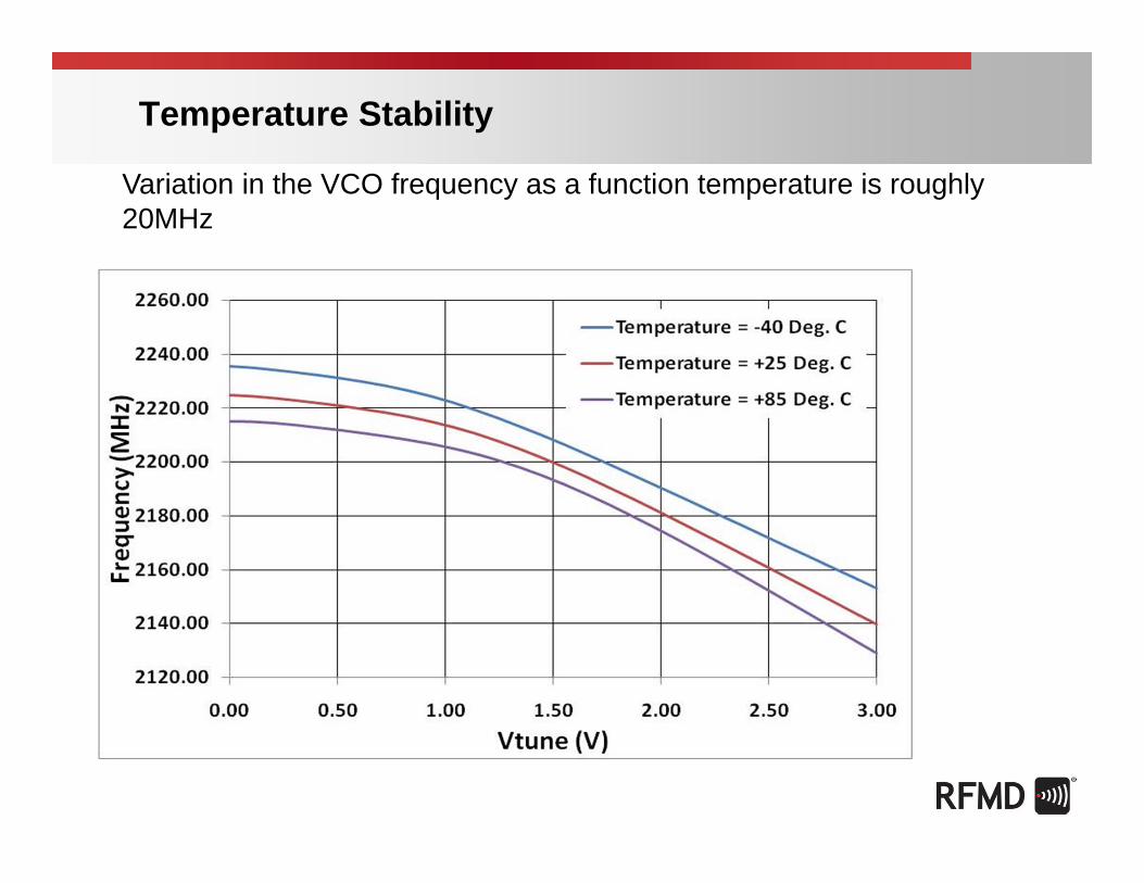
Temperature Stability
Variation in the VCO frequency as a function temperature is roughly 20MHz

Kv Variation
The operating voltage of the VCO is selected such that Kv variation isminimized

Switch-Capacitor Array
• Segmented design to keep the area small while simultaneously providing monotonicity
• Frequency tuning resolution determined by the smallest MIM capacitor allowed
B0
C
B1
2C 4C
B3
8C
B4
16C
B5
32C
B6
32C
B7
32C
Thermometer Coded Elements
Binary Weighted Elements
B2

Unit Element of the Switch-Capacitor ArrayDrain of a switch transistor experiences a negative voltage swing

Unit Element of the Switch-Capacitor Array

Charge Pump
• The charge pump was required to work up to 6V• The potential of each isolated P-well ( where M3 and M4 residing) was
adjusted by a tracking circuit

Tracking Circuit Performance Bias voltage of each isolated P-well is a function of the output voltage of the charge pump.
VVSS VVDD

Out of Loop Dividers
VCO frequency can be scaled down using a collection of “out-of-loop” frequency dividers

Calibration
During calibration, number of VCO cycles are counted in one PFD cycle

Measured Synthesizer Performance
Calibration algorithm is virtually instantaneous

Measured Synthesizer Performance
• VCO Phase Noise : -134dBc/Hz @ 600kHz• Better phase noise using “out-of-loop” dividers

Performance of the Calibration Algorithm
Calibration algorithm can maintain the Vtune within 100mV from what is set by the VC word

Die Micrograph

Performance Summary
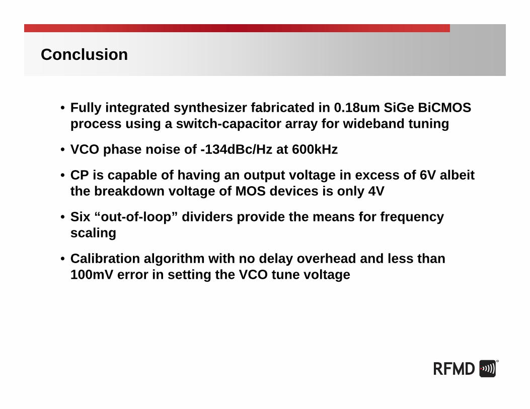
Conclusion
• Fully integrated synthesizer fabricated in 0.18um SiGe BiCMOS process using a switch-capacitor array for wideband tuning
• VCO phase noise of -134dBc/Hz at 600kHz
• CP is capable of having an output voltage in excess of 6V albeit the breakdown voltage of MOS devices is only 4V
• Six “out-of-loop” dividers provide the means for frequency scaling
• Calibration algorithm with no delay overhead and less than 100mV error in setting the VCO tune voltage

Auxiliary: Tank Voltage and Current
Voltage-limited operation with swing twice as large as supply
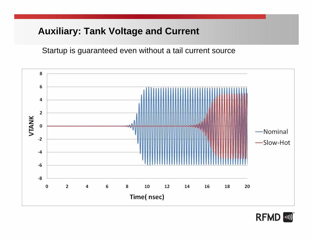
Auxiliary: Tank Voltage and Current
Startup is guaranteed even without a tail current source

Auxiliary: VCO FOM
fLPkT
ff
d
2
0log10FOM2 fLPkT
fBW
d
2
log10FOM1
fLf
fBW
20log10FOM3
This Work [3] [1] [2] [4]
FOM1 (dB) -9.6 2.0 -15.7 -4.5 0.7FOM2 (dB) 6.0 8.2 4.5 16.7 10.9FOM3 (dB) 197.1 193.4 193.0 190.1 189.8
• FOM1: Bandwidth, Power Dissipation and Phase Noise• FOM2: Frequency, Power Dissipation and Phase Noise• FOM3: Bandwidth, Frequency, Phase Noise

Auxiliary: Out-of-loop Dividers
• CML logic based• Design emphasis on low noise floor
• Large signal amplitudes and faster slew rates are necessary• Dominant noise source are in clock buffering and output paths• Critical to reduce the current reference bias noise