a low-power two-line inversion method for driving lcd · pdf filenormal frame rate of tvs is...
TRANSCRIPT

JOURNAL OF SEMICONDUCTOR TECHNOLOGY AND SCIENCE, VOL.16, NO.4, AUGUST, 2016 ISSN(Print) 1598-1657 http://dx.doi.org/10.5573/JSTS.2016.16.4.481 ISSN(Online) 2233-4866
Manuscript received Oct. 22, 2015; accepted Mar. 29, 2016 1 College of Information and Communication Engineering, Sungkyunkwan University, Korea 2 Display Solution Development, SAMSUNG Electronics. E-mail : [email protected]
A Low-Power Two-Line Inversion Method for Driving LCD Panels
Sung-Pil Choi1,2, Kee-Won Kwon1, and Jung-Hoon Chun1
Abstract—A new two-line based inversion driving method is introduced for low power display-driver ICs. By inserting a timing offset between the chopper stabilization and the alternation of LCD polarity, we can reduce power consumption without noticeable degradation in the display quality. By applying the proposed scheme to 12" LCD applications, we achieved 7.5% and 27% power saving in the display-driver IC with white and black patterns, respectively. Index Terms—DDI, LCD driver IC, slew rate, high uniformity, charge recycling
I. INTRODUCTION
As mobile applications such as cellular phones, tablet PCs, and laptop computers are widely used, low-power consumption for portable displays becomes an essential factor for mobility and portability. To reduce the power consumption while enhancing or maintaining the image quality, large LCD panels for TVs or monitors adapt delicate techniques such as local backlight dimming [1], adaptive color and contrast (ACC), and a dynamic frame rate [2, 3]. The local backlight dimming decreases the power consumption by diminishing the luminance of backlight when a partial image of a corresponding position exhibits black or dark gray. On the other hand, the dynamic frame rate technique saves power by lowering the frame rate when a display exhibits a still
image. It is suitable for TV applications, because the normal frame rate of TVs is set two or four times as high as that of portable applications, to suppress flicker noises [4]. However, the local dimming and dynamic frame rate techniques are not suitable for portable devices. The local backlight dimming inevitably increases the display thickness, and the dynamic frame rate technique most likely accompanies severe flicker noises because the normal frame rate of portable devices is as low as 60 Hz.
In mobile applications, the line-inversion method has been prevalently adopted because it is relatively simple and consumes much less power than the dot-inversion method. Even though the line-inversion method consumes less power compared to the dot-inversion method, it still consumes a considerable amount of dynamic power because the polarity changes at every vertical line. To alleviate this power consumption issue, LCD manufacturers have adopted compromised solutions such as two-line inversion, 1+2-line inversion, and staggered N-line inversion. The line-inversion method has other drawbacks such as cross-talk and flicker; therefore, the image quality can be degraded [5-7]. On the other hand, chopper stabilization is widely used to suppress the offset noise in display-driver ICs (DDIs). Because the phase shift for chopping within the same raster period can exhibit color-discordance which can be detected by human eyes, the chopping switches turned on and off alternately, only when the inversion polarity is changed. That is, the chopper stabilization should be synchronized with the line inversion.
In this paper, we propose a new method of integrating the line inversion and chopper stabilization [9]. By inserting a timing offset between the two functions, we can efficiently eliminate any image degradation while

482 SUNG-PIL CHOI et al : A LOW-POWER TWO-LINE INVERSION METHOD FOR DRIVING LCD PANELS
sustaining 2-line based inversion method for low-power consumption. The proposed circuit and its operation mechanism will be described in Section 2. Simulation results and measurement results will be discussed in Sections 3 and 4, respectively, followed by the conclusion in Section 5.
II. PROPOSED LINE-INVERSION DRIVING
METHOD
A single DDI consists of hundreds of voltage followers that should have identical electrical characteristics so that there is no color discordance during operation. However, these voltage followers have an inherent systematic offset due to process variations, and this offset problem becomes worse as multiple DDIs are employed in large-scale integration, as shown in Fig. 1. To overcome this offset problem, two basic techniques, auto-zeroing and chopper stabilization, have been used. Among them, chopper stabilization exhibits low baseband noise and does not need an additional capacitor; therefore, it is used widely in the DDI. Fig. 2 shows the chopper stabilization, which has two-phase operation. In each phase, two pairs of switches are alternately turned on and off. As mentioned before, the timing controller usually does not assign any controlling signal just for chopping stabilization. Thus, the DDI changes the phase of chopping in synchronicity with the polarity of the LCD panel
The DDI receives a “polarity” signal from the timing controller and inverts the output of the voltage follower. Hereafter, “positive polarity” means that the output of the voltage follower is high, and “negative polarity” means that the output of the voltage follower is low. Fig. 3(a)
and (b) show the timing diagrams for the conventional one-line-based inversion and the conventional two-line-based inversion, respectively. The output of the voltage follower reaches VH+ (–) when the polarity is positive and the offset phase Φ in Fig. 2(a) is high (low). Likewise, the output of the voltage follower reaches VL+ (–) when the polarity is negative and Φ in Fig. 2(a) is high (low). Because the alternation of polarity is a dominant power consumption factor in LCD driving, the two-line-based inversion, in which the frequency of the polarity and offset phase alternation is halved as shown in Fig. 3(b), is widely used to reduce power consumption. It should be noted that the outputs of the even numbered voltage followers (Y2k) are depicted in Fig. 3, and Y2k+1 is the flipped image of Y2k in the y-direction.
Because human eyes can detect a smaller difference in luminance at a lower frequency, sparse inversion with a considerable systematic offset invokes observable vertical flickers. In general, vertical flickers are caused by a limited slew-rate and the offsets of the voltage followers. Fig. 4(a) and (b) respectively show typical patterns of the vertical flicker caused by the slew-rate problem and the flicker in two-line-based inversion due to the systematic offset of the voltage followers. Until now, the vertical flicker due to the offsets has no specific solution except for increasing the frame frequency or the size of the transistors in the voltage followers. These solutions have the drawbacks of increased power consumption or increased chip-size.
Fig. 1. Exemplary interface arrangement of display-driver ICs (Yk is the output of the kth voltage follower).
(a)
Fig. 2. (a) Schematic diagram of the chopper stabilization of a voltage follower in a DDI, (b) the mechanism of chopper stabilization.

JOURNAL OF SEMICONDUCTOR TECHNOLOGY AND SCIENCE, VOL.16, NO.4, AUGUST, 2016 483
With the same frame frequency two-line-based inversion is more susceptible to the image degradation induced by vertical flickers than one-line-based inversion. In order to overcome this image degradation problem while maintaining low power consumption, we propose a new two-line-based inversion method, as illustrated in Fig. 5. In Fig. 5, Y2k and Y2k+1 represent the even and odd number indexed voltage followers, respectively. In the proposed method, all the voltage followers change their offset phase at the exact middle point of each polarity period. For example, each positive polarity period of Y2k starts with negative offset phase (VH-), but the offset phase changes to positive (VH+) at the midpoint of each positive polarity period. Y2k+1 is the flipped image of Y2k in the y-direction. However, the transition of the LCD polarity still invokes every other vertical line to reduce the power consumption as in the conventional two-line-based inversion. Thus, we can
dramatically reduce the offset-induced flicker phenomenon using the proposed inversion method while maintaining the low power consumption of the conventional two-line inversion.
As shown in Fig. 5, the key technique of our proposed scheme is separating the transition of the offset phase from the transition of the polarity in the time domain. Fig. 6 shows how the timing control signals are generated. In conventional two-line inversion, the “Polarity_in” signal
from the timing controller has a period of 4×THSYNC.
Here, THSYNC is the period of “Hsync”. We first synchronize “Polarity_in” with “Hsync”, generating “Polarity” which directly controls the polarity of the voltage-follower output. “Polarity” is divided by two and fed into the non-overlapping generator in Fig. 6(c). The output of the non-overlapping generator, Φ, controls the chopping switches in Fig. 2 to cancel the offset. Fig. 7 shows the timing diagram of the aforementioned signals.
In the proposed two-line-based inversion scheme, there are two pairs of control signals (Φ2K and Φ2K+1) for chopper stabilization. Because “Polarity” is delayed by THSYNC before it is fed into the non-overlapping generator, the rising edge of Φ2K lags behind the rising edge of “Polarity” by THSYNC. On the contrary, the rising edge of Φ2K+1 leads the rising edge of “Polarity” by THSYNC because of the additional inverter before the non-overlapping generator. In Fig. 7, the conceptual waveforms of Φ2K and Φ2K+1 are depicted and compared
(a)
(b)
Fig. 3. Timing diagram of the voltage follower output (a) with conventional one-line-based inversion, (b) with conventional two-line-based inversion.
(a) (b)
Fig. 4. Example of degraded display images with vertical flicker due to (a) the slew rate problem, (b) the systematic offset of the voltage follower.
(a)
(b)
Fig. 5. Conceptual timing diagrams of the voltage follower outputs with the proposed two-line-based inversion (a) for even number indexed voltage followers, Y2K, (b) for odd number indexed voltage followers, Y2k+1.
484 SUNG-PIL CHOI et al : A LOW-POWER TWO-LINE INVERSION METHOD FOR DRIVING LCD PANELS
with the conventional Φ. By inserting timing skews between “Polarity” and Φ2K / Φ2K+1, we can also considerably reduce the EMI impact and coupling noise to the virtual ground, improving the signal integrity of the DDI.
III. SIMULATION RESULTS
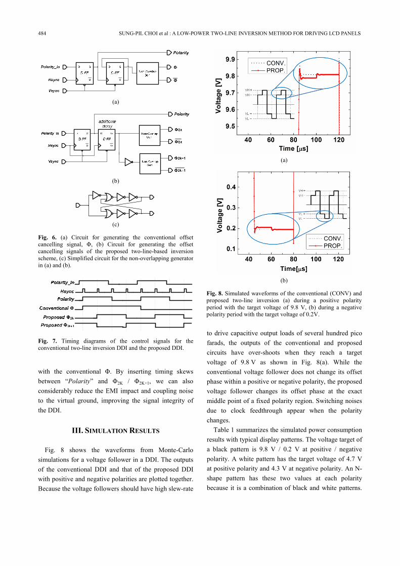
Fig. 8 shows the waveforms from Monte-Carlo simulations for a voltage follower in a DDI. The outputs of the conventional DDI and that of the proposed DDI with positive and negative polarities are plotted together. Because the voltage followers should have high slew-rate
to drive capacitive output loads of several hundred pico farads, the outputs of the conventional and proposed circuits have over-shoots when they reach a target voltage of 9.8 V as shown in Fig. 8(a). While the conventional voltage follower does not change its offset phase within a positive or negative polarity, the proposed voltage follower changes its offset phase at the exact middle point of a fixed polarity region. Switching noises due to clock feedthrough appear when the polarity changes.
Table 1 summarizes the simulated power consumption results with typical display patterns. The voltage target of a black pattern is 9.8 V / 0.2 V at positive / negative polarity. A white pattern has the target voltage of 4.7 V at positive polarity and 4.3 V at negative polarity. An N-shape pattern has these two values at each polarity because it is a combination of black and white patterns.
(a)
(b)
(c)
Fig. 6. (a) Circuit for generating the conventional offset cancelling signal, Φ, (b) Circuit for generating the offset cancelling signals of the proposed two-line-based inversion scheme, (c) Simplified circuit for the non-overlapping generator in (a) and (b).
Fig. 7. Timing diagrams of the control signals for the conventional two-line inversion DDI and the proposed DDI.
(a)
(b)
Fig. 8. Simulated waveforms of the conventional (CONV) and proposed two-line inversion (a) during a positive polarity period with the target voltage of 9.8 V, (b) during a negativepolarity period with the target voltage of 0.2V.

JOURNAL OF SEMICONDUCTOR TECHNOLOGY AND SCIENCE, VOL.16, NO.4, AUGUST, 2016 485
Because the proposed method is based on the conventional two-line inversion, it considerably reduces the dynamic power consumption by doubling the polarity period comparing with the conventional one-line inversion. Because a black pattern requires the largest voltage swing among three different patterns, the power consumption for a black pattern is 2.2 times higher than the power consumption for a white pattern. Therefore the amount of power saving with the conventional and proposed two-line inversion methods can be maximized when they deal with black patterns. The proposed two-line inversion consumes slightly higher dynamic power than the conventional two-line inversion, because the alternation frequency of Φ2K and Φ2K+1 is doubled.
IV. FABRICATION AND MEASUREMENT
The DDI with the proposed inversion scheme was fabricated using a 130 nm CMOS process, and was applied to a 12” normal white LCD panel for a tablet application. Fig. 9 shows the layout of the proposed DDI. There are 720 voltage followers in one DDI and six DDIs in the LCD panel.
Fig. 10 shows the measured output waveforms of a conventional DDI when the two-line-based inversion is used. The waveforms are not as clear as the simulation results, but it is noticeable that the voltage level is sustained within one polarity region. In addition, the impacts of clock feedthrough can be observed as expected from the simulated results. It should be noted that the voltage spikes at the middle point of the high polarity are due to the charge compensation that does not have any influence on the display quality.
The output waveforms of the voltage followers driven by the proposed circuit are shown in Fig. 11. We can clearly see that Φ2K changes from VH– to VH+ in the middle of the positive polarity in Fig. 11(a). Also, Φ2K+1
Table 1. Simulated power consumption of the DDI with black/white/N-shaped patterns (THSYNC = 20㎲)
Patterns Black White N-shaped Conventional
two-line inversion 38.4 mW 17.2 mW 29.0 mW
Conventional one-line inversion 69.7 mW 31.3 mW 57.4 mW
Proposed two-line inversion 40.1 mW 18.5 mW 30.2 mW
Fig. 9. Layout of the display-driver IC with our proposed inversion scheme.
VH+
VH-
Y2K
HSYNC
Fig. 10. Measured output waveform of the conventional DDI with a black pattern.
VH+
VH-
Y2K
HSYNC
(a)
VL+
VL-Y2K+1
HSYNC
(b)
Fig. 11. Measured output waveform of the proposed DDI with ablack pattern (a) Y2K with positive polarity, (b) Y2K+1 with negative polarity.

486 SUNG-PIL CHOI et al : A LOW-POWER TWO-LINE INVERSION METHOD FOR DRIVING LCD PANELS
changes from VL– to VL+ at the middle of the negative polarity in Fig. 11(b). In other words, the phase shift for the chopper stabilization occurs at the middle of each polarity, as explained in Fig. 5. We could confirm that the LCD panel with the proposed DDI does not have any noticeable flickers.
In order to check whether the proposed DDI introduces any degradation such as cross-talk to display panel, a test board was also fabricated and integrated with the display panel as shown in Fig. 11(a). The test board consists of a timing controller, an FPGA and an EEPROM access module for modifying display patterns. Compared with the one-line based inversion, the proposed scheme consumes much less power while maintaining the same display quality. The flicker phenomenon could be suppressed by adopting the conventional one-line inversion scheme, but the dynamic current consumption increased as summarized in Table 2. The measured total power numbers are higher than the simulation results because other analog circuits such as a
resistive DAC consume considerable power. Another discrepancy between the simulation results and the measured results is that the power consumption with N-shaped patterns is close to the power consumption with black patterns, because level shiting operation between a black pattern and a white pattern consumes considerable power which was not counted in the simulation. Comparing with the conventional one-line inversion, the proposed scheme saves 27% of the total power with black patterns, 19% with N-shaped patterns, and 7.5% with white patterns.
V. CONCLUSIONS
We proposed a new LCD driving method that separates the phase shift of chopper stabilization from the alternation of the LCD polarity in two-line based inversion scheme. The fabricated DDI with the proposed two-line inversion does not show any degradation in the display quality, but it consumes 7.5% ~ 27% lower power than the DDI with the conventional one-line inversion. This technique can be an easy–to-adopt solution for removing vertical defects in portable LCD panels.
ACKNOWLEDGMENTS
This research was supported by the Ministry of Science, ICT and Future Planning, Korea, under the ITRC support program (IITP-2016-H8501-16-1010), and the Basic Science Research Program through the National Research Foundation of Korea (2011-0014267).
REFERENCES
[1] W. C. Cheng, M. Pedram, “Power minimization in a backlit TFT-LCD display by concurrent brightness and contrast scaling,” Proc. of Conf.
FPGA
EEPROMaccess
Timing Controller
backlight
Display panel
(a)
Proposed 6 DDIs
(b)
Fig. 12. Verification setup and result (a) a test board to verify display quality of the display panel with the proposed DDI, (b) evaluation pattern of the display panel with the proposed DDI, which does not show any degradation including cross-talk.
Table 2. Measured power consumption of the DDI for several typical patterns (frame freq. = 60 Hz)
Patterns Black White N-shaped Flicker Conventional
two-line inversion 82.5 mW 66.0 mW 80.6 mW Yes
Conventional one-line inversion 115.5 mW 73.3 mW 102.0 mW No
Proposed two-line inversion
84.3 mW (27%↓)
67.7 mW (7.5%↓)
82.9 mW (19%↓) No

JOURNAL OF SEMICONDUCTOR TECHNOLOGY AND SCIENCE, VOL.16, NO.4, AUGUST, 2016 487
Design, Automation and Test in Europe, pp. 10252-10259, 2004
[2] H. S. Nam, S. W. Lee, “Low-power liquid crystal display television panel with reduced motion blur,” IEEE Transactions on Consumer Electronics, vol. 56, no. 2, pp.307-311, 2010
[3] I. S. Choi, H. J. Shim, N. H. Chang, “Low-power color TFT-LCD display for hand-held embedded systems,” Proc. of Conv International Symposium on Low Power Electronics and Design, pp.112-117, 2002
[4] S. H. Chan, T. Q. Nguyen, “LCD Motion Blur: Modeling, Analysis, and Algorithm,” IEEE Transactions on Image Processing, vol. 20, no. 8, pp.2352-2365, 2011
[5] F. R. Libsch, A. Lien, “Low-power Driving Method for Reducing Cross-talk in High Resolution TFT-LCDS,” International Workshop on AMLCDs, pp. 72-75, 1995
[6] Y. C. Jeong, C. C. Park, L. S. Kim, “A new crosstalk compensation method in line inversion TFT-LCD’s,” IEEE Transactions on Circuits and Systems, Vol:44, pp. 552 – 555, 1997
[7] J. H. Woo, J. G. Lee, Y. H. Jun, B. S. Kong, “Analysis on panel power consumption of mobile TFT-LCDs based on line inversion driving,” IEEE Internation Conference of Electron Devices and Solid-State Circuits, pp.1-4, 2010
[8] L. Xing, J. Y. You, T. Ebrahimi, A. Perkis, “A Perceptual quality metric for stereoscopic crosstalk perception,” IEEE International Conference on Image Processing, pp. 4033-4036, 2010
[9] S.-P. Choi, G.-C. Hwang, Y.-H. Jun, K.-W. Kwon, and J.-H. Chun, “A Low-Power Two-Line Inversion Method for Driving LCD Panels,” Proc. of IEEE International Conference on Circuits and Systems, pp. 1995-1998, 2012.
Sung-Pil Choi is a senior engineer at Samsung Electronics, Korea. He received his B.S. and M.S. degrees in electrical engineering from Seoul National University, Korea, in 2000 and 2002, respectively. In 2015, he received the Ph.D. degree in
electrical engineering from Sungkyunkwan University. From 2001 to 2003, he worked at TomatoLSI, Seoul,
where he developed several LCD driver ICs for mobile application. He moved to Samsung Electronics in 2004 and worked in the areas of Display Driver IC. Dr. Choi has been developing numerous Display Driver ICs for large display panel. His current research is UHD & QUHD driving technology and low-power design of a Display Driver IC for tablet display.
Kee-Won Kwon received his B.S. degree in metallurgical engineering from Seoul National University, in 1988. He also received his M.S. degree in electrical engineering and the Ph.D. degree in materials science and engineering from Stanford Uni-
versity, Stanford, CA, in 2000 and 2001, respectively. From 1990 to 1995, he was with Samsung Electronics, Giheung, Korea, where he developed tantalum pentoxide dielectric thin films and successfully implemented them into the commercial product of DRAM. In 2000, he worked for Maxim Integrated Products, Sunnyvale, CA where he was involved in two projects of data converting circuit design. He rejoined Samsung Electronics in 2001, and worked in the areas of high performance DRAM designs including Rambus DRAM and XDR DRAM. In 2007, he moved to Sungkyunkwan University, where he is doing research on memory IP design, and low power high speed circuit solutions for analog and mixed-signal devices.
Jung-Hoon Chun is an Associate Professor at Sungkyunkwan University, Korea. He received the B.S. and M.S. degrees in electrical engineering from Seoul National University, Korea, in 1998 and 2000, respectively. In 2006, he received the Ph.D. degree in
electrical engineering from Stanford University. From 2000 to 2001, he worked at Samsung Electronics where he developed BiCMOS RF front-end IC for wireless communication. From 2006 to 2008, he was with Rambus Inc. where he worked on high-speed serial interfaces such as FlexIOTM, XDRTM, XDR2TM etc. Dr. Chun also consults for several IC design and foundry companies in Korea and Silicon Valley. His current research includes high-speed serial link, image sensors, on-chip ESD protection and I/O design, new memory devices, etc.