a micropower ultra-wideband radar profiling system
TRANSCRIPT

Univers
ity of
Cap
e Tow
n
A Micropower Ultra-Wide band RADAR Profiling System
Yu-Ming Alvin Chang
A dissertation submitted to the Department of Electrical Engineering,
University of Cape Town, in fulfilment of the requirements
for the degree of Master of Science in Applied Science.
Cape Town, August 2006

The copyright of this thesis vests in the author. No quotation from it or information derived from it is to be published without full acknowledgement of the source. The thesis is to be used for private study or non-commercial research purposes only.
Published by the University of Cape Town (UCT) in terms of the non-exclusive license granted to UCT by the author.
Univers
ity of
Cap
e Tow
n

Declaration
I declare that this dissertation is my own, unaided work. It is being submitted for the
degree of Master of Science in Applied Science in the University of Cape Town. It has
not been submitted before for any degree or examination in any other university.
Signature of Author ........................ .
Cape Town
31 August 2006
Signature Removed

Abstract
Ultra-wideband (UWB) technology can be used in many applications, including radar,
communications, and geo-location. In this dissertation, UWB technology is utilized to
directly generate sub-nanosecond pulses with more than 1 GHz bandwidth to implement
radio detection and ranging (RADAR) for distances up to 5 or 10 metres.
This low-cost, rnicropower radiation, short-range radar profiling system consists of the
radar circuitry, the data-acquisition subsystem, the signal processing subsystem and the
graphical user interface. Additional modules such as a front-end RF amplifier can be
integrated into the complete system. The performance was analysed, particularly the cir
cuitry performance and system performance. The capability for detecting metal objects
was demonstrated, along with discussion of preliminary "seeing-through-wall" experi
ments.
11

Thanking my parents
111

Acknowledgments
This research would not have been possible without the financial assistance from the
CSIR and the NRF. It also would not have been possible without the research facilities
and equipments provided by the University. Foremost, it would not have been possible
without the guidance nd supervision from Dr. Andrew J. Wilkinson.
I thank you all.
IV

Contents
Declaration
Abstract
Acknowledgements
List of Symbols
Nomenclature
1 Introduction
1.1 Purposes . . . . . . . .
1.2 Structure of The Thesis
1.3 Literature Review . . .
1.3.1 UWB Technology for Radar
1.3.2 Wideband Antennas Suitable for UWB Technology .
2 Short Pulse UWB Principles and Implementation Architecture
2.1 Conventional Pulse Radar .
2.2 Operation of UWB Radar .
2.3 Signal Model for an UWB Radar .
3 Signal Processing
3.1 Background Removal (Difference Imaging)
3.2 Out-of-Band Signal Nulling
3.3 Matched Filter (Correlator)
3.4 Deconvolution Filter
3.5 Window Functions .
4 Circuits Simulation and Implementation
4.1 PRF Signal Generator ..... .
v
ii
iv
xiv
XV
1
1
2
3
3
3
5
5
6
7
12
12
12
12
13
13
16
17

402 Transmitter 0 0 0 0 0 0 0 0 0 0 0 0 0 0 0 0 0 0 0
403 Manual Delay Line and Fast Sampler-Averager
17
21
4.4 Computer-Controlled Variable Delay Line and Fast Sampler-Averager 23
405 Post-Sampler Amplifier 0 0 0 0 0 0 0 0 0 0 0 0 0 0 0 0 0 0 0 0 0 0 0 0 0 31
5 System Integration 34
501 RADAR Circuit 0 34
502 NI-DAQ Card 0 0 35
503 Front-End RF Amplifier
5.4 Antennas 0 0 0 0 0 0 0 0
5.401 Bow-Tie Antennas
5.402 Grid Antennas
36
39
39
41
6 Software System 42
42
42
42
44
45
46
7
601 Software Design 0
602 Software Implementation
60201 Graphical User Interface
60202 Digital Signal Processing 0
603 Software Operation 0 0 0 0 0 0 0 0
60301 Distance Conversion and an Example
Results and Performance
701
702
703
7.4
705
706
707
708
709
Achievable Pulse Bandwidth • 0 • • • 0 •
Limitations of Simple Antenna Structures
Processed Bandwidth
Peak Power Radiated
7.401 Simulation
7.402 Oscilloscope Measurement 0
Averaged Power Radiated 0 0 0 0 0 0
Limitation of Indoor Measurements
Capability f r Detecting Metal Objects 0
70701 Performance Without RF Amplifier
70702 Performance With RF Amplifier
Detection through Obstacles • 0 ••••
70801 Detection through Wooden Partition
7 0802 Detection through Cement Wall
Noise Performance 0 0 0 0 0 0 0 0 0 0 0
so 50
50
51
51
51
52
52
53
53
55
57
57
61
64
64
7010 Achievable Maximum Sweeping Rate and Maximum Speed Detectable 65
Vl

8 Conclusions and Future Work
A Software Source Code
Bibliography
Vll
67
68
71

List of Figures
2.1 Block diagram of an elementary radar system, and some abbreviations
commonly used [27]. . . . . 6
2.2 The UWB radar scheme[47]. 8
2.3 Operation of the "fast sampler" with a fixed delay. . 8
2.4 UCT UWB radar scheme (Mono-static). 9
2.5 UCT UWB radar scheme (Bi-static). . . 9
3.1 Hanning window; W [k + 1] = 0.5 (1- cos (21r n~ 1 )) , k = 0, · · · , n - 1. 14
3.2 Hamming window; W [k + 1] = 0.54-0.46 cos (21r n~l ) , k = 0, · · · , n-
1. . . . . . . . . . . . . . . . . . . . . . . . . . . . . . . . . . . . . . . 14
3.3 Blackman window; w [k + 1] = 0.42-0.5cos (27r n~l)+0.08cos (47r n~l), k = 0, · · · , n- 1. . . . . . . . . . . . . . . . . . . . . . . . . . . . . . . . . 15
4.1 Agilent Infinium 54833A DSO
4.2 The noise modulated pulse generator used in [47, 30, 1].
16
17
4.3 The simulated output voltage at node "out" (in Figure 4.2) is plotted as a
function of time. The period is approximately 360 ns. . . . . . . . . . . . 18
4.4 The measured output voltage at node "out" (in Figure 4.2) is plotted as a
function of time. The period is approximately 420 ns.
Vertical (voltage) scale 1.00 VI Offset 2.46V.
Horizontal (time) scale 200 ns .. . . . . .. .. .. . 18
4.5 Noise generated from the left-half of the circuit shown in Figure 4.2. 19
4.6 The measured noise generated from left-half of the circuit shown in Fig-
ure 4.2.
Vertical (voltage) scale 500 mV I Offset 1.629V.
Horizontal (time) scale 200 ns.
4.7 The transmitter used in [47]. .
4.8 UCT UWB Radar Transmitter
4.9 Equivalent SPICE circuit for a dipole antenna [17].
4.10 The simulated waveform at node C4-R10-U5 ....
Vlll
19
20
20
21
22

4.11 The measured waveform at C4-R10-U5 (lower waveform) with reference
to the master clock (upper waveform).
Vertical (voltage) scale 2.0 V
Offset -1.47 V (master clock) I Offset 4.81 V (C4-R10-U5).
Horizontal (time) scale 200 ns. . . . . . . . . . . . . . . . . . . . . . . . 22
4.12 Wave form at node C5-Rll-Q4 feeding into the base of the transistor Q4. 23
4.13 Simulated pulse using 2N5109 transistor across son load ..
4.14 The measured waveform generated by 2N5109.
Vertical (voltage) scale 500 mV I Offset 0.
Horizontal (time) scale 2 ns: ............... .
4.15 Simulated pulse using BFR91A transistor across son load.
4.16 The measured waveform generated by BFR91A.
Vertical (voltage) scale 500 mV I Offset 0.
24
24
25
Horizontal (time) scale 2 ns . . . . . . . . . . . . . . . . . . . . . . . . . 25
4.17 The measured waveform generated by BFR91A with DFT analysis be-
neath.
Vertical (voltage) scale 500 mV I Offset -379 mV.
DFT (wattage) scale 20 dBm I Offset -15 dBm.
Horizontal (time) scale 50 ns.
DFT (frequency) scale 200 MHz I Position 1 GHz. . . . . . . . . . . . . 26
4.18 The delay line and the fast sampler connected to a balanced dipole antenna
used in [47]. . . . . . . . . . . . . . . . . . . . . . . . . . 26
4.19 UCT UWB Radar Delay Line and Fast Sampler-Averager . 27
4.20 Reverse voltage v.s. capacitance of MV104. 28
4.21 Voltage vs. Delay . . . . . . . . . . . . . 28
4.22 Sub-circuits CIRCUIT! and CIRCUIT2. . 29
4.23 Thevenin equivalent circuits of CIRCUIT I and CIRCUIT2. . 29
4.24 Discharging circuits. . . . . . . . . . . . . . . . . . . . . . 30
4.25 Thevenin equivalent circuits for the discharging circuits in Figure 4.24. . 30
4.26 Post-Sampler Amplifier used in [47]. . 31
4.27 UCT UWB Post-Sampler Amplifier . 32
4.28 Simplified Schematic of AD620 reproduced from [2]. 33
5.1 UCT UWB radar prototype (Mono-static) 34
5.2 NI-DAQ . . . . . . . . . 35
5.3 Front-End RF Amplifier 36
5.4 Two-Stage Amplification 36
5.5 Gain vs Frequency Response
(Gain in dB) ........ . 37
IX

5.6
5.7
Noise Figure vs Frequency .
Gain vs Frequency Response
(Gain in ratio) . . . . . . .
5.8 Noise Figure vs Frequency
(Te in Kelvin) ...... .
5.9 GPR Antenna (50- 400 MHz)
5.10 Twin-bowtie Antenna #1 (1 - 2 GHz) with a flare angle smaller than
40°made by [45]. . . ..
5.11 Twin-bowtie Antenna #2 (1- 2 GHz) with a flare angle wider than 40°made
37
38
38
39
40
by [45]. . . . . . . . . . . . . . . . . . . . . . . . . . . . . . . . . . . . 40
5.12 Plot of measured gain vs. frequency of the twin-bowtie antenna with a
flare angle smaller than 40°as measured by [45]. . . . . . . . . . . . . . . 40
5.13 Plot of measured gain vs. frequency of the twin-bowtie antenna with a
flare angle wider than 40°aS measured by [45]. . . . . . . . . . . . . . . . 40
6.1 Software design.
6.2 Software Interface .
6.3 Background snapshot
6.4 Echo from calibration target used to create deconvolution filter
6.5 Unprocessed echo from a plate reflector .
6.6 Match filtered with no windowing applied
6.7 Deconvolution filtered with no windowing applied .
6.8 Deconvolved and Hanning windowed ...... .
7.1 Instantaneous power of the simulated waveform of Figure 4.15 ..
7.2 Instantaneous power across 500 of the pulse waveform captured in Figure _ V(t) 2
4.16. P(t) - R .
7.3 Experiment Setup .
7.4 Target at 50cm without RF amplifier.X-axis: Sample (spans from -2.33m
43
44
47
47
48
48
49
49
52
53
55
to 9.35m).Y-axis: Voltage (V). . . . . . . . . . . . . . . . . . . . . . . . 56
7.5 Target at 80cm without RF amplifier.X-axis: Sample (spans from -2.33m
to 9.35m).Y-axis: Voltage (V). 56
7.6 No Target with RF amplifier ..
7.7 Target at l.Om with RF amplifier . .
7.8 Target at 1.5m with RF amplifier ..
7.9 Target at 2.0m with RF amplifier ..
7.10 Target at 2.5m with RF amplifier . .
7.11 Target at 3.0m with RF amplifier . .
X
57
58
58
59
59
60

7.12 Targets at l.Om and 2.5m with RF amplifier.
7.13 Partition at l.Om. . . . . . . . . . . . . . .
7.14 Target at 1.5m. (The partition located at l.Om is not visible after back-
60
61
ground subtraction.) . . . . . . . . . . . . . . . . . . . . . . . . . . . . . 62
7.15 Target at 2.0m. (The partition located at l.Om is not visible after back
ground subtraction.) . . . . . . . . . . . . . . . . . . . . . . . . . . . . . 62
7.16 Target at 2.5m. (The partition located at l.Om is not visible after back
ground subtraction.) . . . . . . . . . . . . . . . . . . . . . . . . . . . . . 63
7.17 Target at 3.0m. (The partition located at l.Om is not visible after back
ground subtraction.) . . . . . . . . . . . . . . . . . . . . . . . . . . . . . 63
Xl

List of Ta les
5.1 Grid Antennas . . . . . . . . . . . . . . . . . . . . . . . . . . . . . . . . 41
7.1
7.2
7.3
Metal Objects Tested
Decrease due to the placement of the partition ..
Signal-to-Noise ratio at different ranges. . ...
xii
54
61
64

Xlll

List of Symbols
b(t)
B
c
fmax
f PRF
fc
fH h T sweep
f(t)
f A/D
f D/A
h(t)
Hrx(w)
HRx(w)
r(t)
R
Ra
R jar- f ield
Ro
Rmax
t
Vmax
v(t)
W(w) (3
b(t)
((t)
TCharge
TDischarge
Background snapshot
Bandwidth-limited impulse
Speed of light
M ximum sweep rate
Pulse repetition frequency
C t-off frequency
Highest frequency component
L west frequency component
Sweep period
Filter snapshot/template
AID sampling frequency
D/ A sampling frequency
Impulse response
Impulse response of the TX antenna
Impulse response of the RX antenna
Raw echo
Range of interest
Antenna load
Far-field distance
Maximum operating range
Maximum unambiguous range
Delay of interest
Pulse repetition interval
Total delay range
Noise temperature
Maximum speed detectable
Returned echo without the background
Windowing function
Band of interest
Dirac delta
Impulse response of the scene
Active charge time
Passive discharge time
XIV

Nomenclature
AID-Analogue to digital converter.
Bandwidth-Also called "occupied bandwidth" is the frequency range within which
some specified fraction, say 90 or 99 percent, of the total signal energy lies. This may
be defined for a single pulse, if all pulses are the same, or for a group of pulses that are
processed together to yield a single decision. The upper limit of this range is denoted here
by f H and the lower limit by h. Beamwidth-The angular width of a slice through the main-lobe of the radiation pattern
of an antenna in the horizontal, vertical or other plane.
Bistatic radar-A kind of radar utilizing two separate antennas - one for transmitting
and another for receiving RF signals.
Centre frequency-A frequency calculated as !H~h.
D/ A-Digital to analogue converter.
DAQ-Data acquisition.
DSO-Digital storage oscilloscope.
DSP-Digital signal processing.
Fractional bandwidth-A ratio between bandwidth and centre frequency denoted as 2(JH-fL)
fH+fL •
GPR-Ground penetrating radar.
GUI-Graphical user interface.
10-Input and output.
I/O-Input or output.
Maximum unambiguous range-The maximum distance up to where targets can be
unambiguous! y detected.
Monostatic radar-A kind of radar utilizing a single antenna for both transmitting and
receiving RF signals.
Monolithic-Single-ended.
PLL-Phase-locked loop.
PRF-Pulse repetition frequency.
Range-The radial distance from a radar to a target.
RF-Acronym of Radio Frequency.
XV

RX-Receiver/received.
Simulation Program with Integrated Circuits Emphasis (SPICE)-A general purpose
analog circuit simulator. Various circuit simulators, such as Protei, OrCAD, and Switcher
CAD III (LTspice) are based on SPICE.
T-R switch-A switch that activates either TX or RX circuits at any given time, but not
both.
TX-Transrnitter/transrnitted.
Ultra-Wideband (UWB)-A term used to describe RF signals with fractional bandwidth
2:20%.
XVI

Chapter 1
Introduction
Ultra-wideband (UWB) technology by definition refers to radio-frequency (RF) systems
utilizing signals with a fractional bandwidth 2:20% of the centre frequency [12]. Direct
generation of base-band pulses is the simplest method of generating such signals. Re
cently UWB technology has drawn considerable attention in the radar context [38, 46, 49,
53]. Such radar systems typically generate short pulses of duration less than 1 ns at high
pulse repetition rates of several MHz, depending on the desired unambiguous operating
range. Several UWB pulsed designs have been reported in the literature with bandwidths
exceeding 1 GHz, which suggests that UWB technology can be used to produce a low
cost, high resolution radar for short-range applications. Applications of UWB pulsed
technology include radar, communication systems and geo-location.
UWB radar and communications systems are of particular interest in military applications
as they have the benefit of low probability of interception and detection, a consequence of
extremely low spectral power density (Watts per Hz). Narrow-band communication links
may be more easily detected, although the information streams can be encrypted.
Short-range UWB radar finds application in vehicle piloting, ground penetrating radar,
detection of motion through walls, and detection of weapons [38, 46, 49, 53]. Extremely
simple architectures have been developed, which result in compact, low power consump
tion devices for short range applications.
Geo-location (tagging) is also one of the uses of UWB pulse technology for the reasons
such as low production cost due to simple architecture e.g. asset control [8]. The wide
bandwidth allows precise location of tagged objects.
1.1 Purposes
The purposes of this study are as follows:
1. To analyse and implement an ultra-wideband (UWB) pulse transmitter and receiver
sub-system published by [47]. Its pulse repetition frequency (PRF) is roughly
1

2.4 MHz, and can be potentially used in short-range applications such as ground
penetrating radar (GPR) or through-wall imaging/detection (TWIID).
2. Based on the sub-system, to build a complete UWB pulse radar profiling system for
short range radar applications by integrating the sub-system mentioned above with
computerized control and data acquisition systems.
3. To design and implement the necessary software to
(a) control the system in 2 to acquire the raw signal from close vicinity;
(b) process the raw signal to generate down-range profiles.
4. To identify antennas suitable for use with the prototype, and to evaluate the perfor
mance of the system under various conditions.
1.2 Structure of The Thesis
This dissertation is organized as follows:
• The rest of this chapter provides a brief literature review of UWB pulse technology.
• Chapter 2 give an analysis of the principles of short pulse UWB radar and the
architecture in olved; it also shows the reference design by [47], and our design
with modifications and additions.
• Chapter 3 provides a list of signal processing steps required to manipulate captured
raw data to produce down-range profiles.
• Chapter 4 describes the simulation and implementation of the circuits involved.
• Chapter 5 explains the interfacing of various hardware circuits and modules with a
computer system to capture raw data.
• Chapter 6 presents software designed to provide an interface between the user and
the profiling sy tern, and how signal processing codes are implemented.
• Chapter 7 presents results from various testing conditions.
• Chapter 8 concludes this project and identifies possible future research.
2

1.3 Literature Review
The root of UWB radar technology dates back to World War II when pulse radars were
first used to facilitate remote sensing. However, modem UWB radar technology has only
started rapid developing since 1990 after Fullerton, L.W patented an easy method to gen
erate base-band pulses [15] and an implementation of an "UWB Radar Motion Sensor"
patented in 1994 by [30].
This section presents a brief literature survey of UWB technologies found in radar appli
cations, and suitable antenna designs for these applications.
1.3.1 UWB Technology for Radar
Pulsed radar is not a new technology, having been around since World War II. Advances
in semiconductor electronics, have led to the development of short pulse ultra-wideband
(UWB) radar technology [21 , 23, 50]. UWB pulse systems emit short pulses with ex
tremely wide bandwidths, which can exceed 1 GHz, offering considerably finer resolution
than most conventional pulsed radars.
Today, cheap, easily constructed UWB radar designs have become available which elim
inate the need for linear power amplifiers, transmit filters, mixers, PLL, reference oscilla
tor and other components [47]. High/Ultra-high resolution radars which can image with
sub-centimetre precision have been implemented [19, 31]. Vehicular radars are now avail
able which scan surroundings to provide collision detection/avoidance, to adjust damping
reactions according to road surfaces ahead, and to pilot the vehicle without human inter
vention [25].
Ground-penetrating radar (GPR) technology has long been developed [19]. One approach
is called stepped frequency continuous wave radar which involves transmitting sinusoidal
signals with a range of discrete frequencies [19]. This contrasts with a pulsed UWB radar
which transmits signals covering the desired frequency range in one pulse by direct pulse
generation [26, 55].
There is an increasing interest in through-wall imaging/detection (TWIID) systems. Using
a frequency range of 1-3.5 GHz, moving people can be detected through cement walls to
aid police in hostile situations, and rescue workers and firefighters to locate victims buried
under collapsed buildings or trapped beneath snow [56].
1.3.2 Wideband Antennas Suitable for UWB Technology
In order to make effective use of the wide bandwidth generated by the UWB pulses,
pulses must be able to radiate and be received by antennas operating at the corresponding
frequency range. In practice, antennas are almost always the limiting factor in terms of
bandwidth because simple electronic circuits can generate pulses with bandwidths which
far exceed the operating frequency range of the antennas to which they are coupled with.
3

Several UWB-specific antenna references are available such as [14, 24, 41, 42, 43] in
cluding both microwave antennas and magnetic antennas. Simulation of the conventional
dipole for UWB applications[17] and designs of UWB resistively-loaded sensors [32] are
also available. The antennas used in this project are mainly those developed in house in
various student projects [45], others developed as part of a research project [5], as well
as commercial TV antennas operating in VHF and UHF bands (shown in Table 5.1 in
Chapter 4).
4

Chapter 2
Short Pulse UWB Principles and
Implementation Architecture
Ultra-wideband pulsed radar systems operate by transmitting short pulses instead of si
nusoidal wave pulses used in conventional radar systems [24]. UWB technology has the
advantage of simpler hardware and higher fractional bandwidth, compared to conven
tional technology. This chapter gives an overview of the UWB system design including
the operating principles of conventional pulse radar and UWB radar, and an introduction
to the signal processing techniques involved.
2.1 Conventional Pulse Radar
A conventional pulsed radar operates by sending and receiving pulses. It is often neces
sary to translate the signal up in frequency to gain better directionality and to fulfil other
requirements. A typical cycle would consists of two phases: transmitting phase and re
ceiving phase. In the transmitting phase, a pulse is generated and transmitted, after a short
delay cause by the T-R switch, the radar switches into receiving phase and acquires the
returned echoes over a period of time. Then after another short delay caused by the T-R
switch, the system switches into the transmitting phase and the cycle repeats. Figure 2.1
from [27] shows the block diagram of an elementary radar system and some abbreviations
commonly used.
The duration of one cycle is called "Pulse Repetition Interval" (PRI), tPRI in second,
which can be converted to "Pulse Repetition Frequency" (PRF) f PRF = -t 1 in Hz. Since
PRJ
electromagnetic waves travel at the speed of light c ~ 3 * 108m/ s, the PRIIPRF deter-
mines the maximum unambiguous range (the maximum range from which a transmitted
radar pulse can be reflected and received before the next pulse is transmitted) denoted
by R max = ~ = 21;RF which is equivalent to ! P RF = 2~ax . E.g. maximum PRF
values are 500Hz for 300krn range, and 15kHz for 1krn range. However, due to other
constraints, typically pulse repetition frequencies vary from several hundred Hertz for a
5

long range radar (several hundred km in range) to hundreds of kHz for short range radars
(up to 1 km in range) .
Transmitter 1--___,..,_----i ....------l (Tx)
ft +h T-R
switch
!t + 12 + .t'.J
Stable Jocal oscillator (STALO)
RF RF amplifier (Rx)
,. . I
Pulse modulator
ft +h
Frequency f~ synthesizer
IF amplifier
Coherent local oscillator (COLO)
·Baseband'
(e.g. S-hand) First IF
Data processing
mixer (e.g . 70 MHz)
Signal Possible processing detections
AID
Digitized ...._c_<_m_v_er_te_r~ video
, " / Raw \ \ displm I \ ·; ...... _ .....
Figure 2.1: Block diagram of an elementary radar system, and some abbreviations commonly used [27].
2.2 Operation of UWB Radar
The UWB radar prototype implemented is based on a sub-system published by Enrico
M. Staderini [47]. The actual electronic circuits presented in [47] are mainly based on
what was disclosed in a few US patents by L. W. Fullerton [15], and T. E. McEwan [30],
along with experiences of the author himself. Figure 2.2 shows the architecture as it
appeared in [ 4 7]. The block labeled "pulse generator" generates a clock at a frequency of
approximately 2.4 MHz. The pulse train is then fed into two blocks: (1) the "transmitter"
block, which generates short (sub nanosecond) pulses, driving the antenna; and (2) the
"nanosecond delay line", which triggers the sampler. The delayed signal acts as a time
dependent trigger to the "fast sampler" which performs "sample-and-integrate" of the
return echoes at a specific range. Figure 2.3 illustrates the operation of the "fast sampler"
with a fixed delay of 28.548~-LS.
The integration time of the fast-sampler is determined by the resistor-capacitor combi
nation used. It is discussed in detail in section 4.3 of Chapter 4. By deploying the fast
sampler, operating at PRF !PRF = 2.0 MHz, typically it needs l ms to lOms to integrate
6

enough returned echoes at one fixed delay. This, in tum, limits the maximum sweeping
rate f max and maximum speed Vmax at which a moving target can be detected because
the scene must be stationary within the integration time to produce an accurate reading.
Further discussion of the maximum sweeping rate and maximum speed detectable can be
found in Section 7.10 of Chapter 7.
Albeit the limitations, the advantage of such an architecture is largely-reduced direct
sampling requirements of RF signals, i.e. twice the highest frequency component. For
a radar operating at the frequency band up to 2 GHz, if one is to sample directly from
the antennas, the minimum AID sampling requirement is 4 GHz as required by Nyquist
theorem. Instead, UCT UWB radar profiling system requires an AID sampling of a few
kHz; depending on the rate at which the delay is swept from near the nearest to the farthest
range.
To improve the signal to noise ratio, the output of the fast sampler is fed to the "aver
ager", which effectively integrates the returns from several hundred pulses. The proto
type described in [47] is a very basic implementation, in which the delay line is manually
adjusted, to provide a detection at a fixed range.
The UCT UWB radar profiling system developed in this MSc project is a complete system
and capable of providing a real-time down-range profile display updated at two profiles
per second. Figure 2.4 shows a block diagram of the UCT UWB radar profiling system
using the same antenna for both transmission and reception. It operates by sliding the
range gate (varying the delay) with the variable delay circuit whilst sampling the output of
the instrumentation amplifier. A down-range profile is acquired as the range gate is moved
from near to far range. A second block diagram, Figure 2.5, shows the configuration used
for hi-static radar mode in which the transmitter and receiver are connected to separate
antennas. The hi-static mode allowed incorporation of a front-end RF amplifier module
made by [59] into the fast sampler-averager without additional input circuit protection
because the transmitted pulses are never fed into it.
The minimum step of which the delay circuit can increment achievable by this system is
15ps with the current data acquisition hardware. However, smaller steps such as 1ps can
be achieved by using better data acquisition hardware. The implementation and limita
tions of the variable delay line is discussed in detail in Subsection 4.4 of Chapter 4.
2.3 Signal Model for an UWB Radar
A radar may be modelled as a linear system. For any linear system, the output y(t ) may
be related to the input x (t) by convolving the input signal with the impulse response of
the system, i.e.
y(t) l+oo
x (t) @ h(t) = - oo X(T)h(t- T)dT (2.1)
7

pulse generator
ayerager (low pass filter)
nanosecond delay line
Radar signal out
transmitter
rece1Yer
Figure 2.2: The UWB radar scheme[47].
target
500mV.--------------------------------------V~(~n0_15~)------------------------------------,
<l60mV ····· ·-· ···---,··-·-·· -----
'IOOmV
350mV --------------•------------
300mV
250mV
' ' ' 200mV -------------,------------ --------- -- ------ - -------1-------- -- ---:--------------:-------------r-------------:-------------
• I I o I
I I I I • I I I I I I I o
I I I I I I
150mV -- ---- ----- -·- --- -- ------ ~- ------ ----- ... ----- ------- ... ----------- -- .. ----------- --•----- --------I I I I I I
I I I o I I
I I I I I I
> I I I I
o 0 I < I
100mV ·--- ----------·------- ' ' _____ .,. ____________ .. _____________ .. _____________ , ____________ _
' ' I I I I
' ' I I I I
' ' I I I I
' ' o I I I
50mV
' ' ...... --.-: ... -- ... -- . : -'-,:·.:--· ----<.:--<"""'·=-=--~--~- -~- ·=· =--"'-'' -~- -=- ·=·=--=--~--~--=-=--=--~--~--=- "-"-j--
' ' ' ' ' ' ' ' -50mv+--------r--------r-------,--------r------~r-------,--------r--------r-----~
28 .5'10~· 28 .542~· 28.544~· 28 .546 ~· 28.548~· 28 .550~· 28 .552~· 28 .554~· 28 .556~· 28.558 ~·
Figure 2.3: Operation of the "fast sampler" with a fixed delay.
8

_.,
I I
J I
~
L t:..______o
-l - __j
NI-DAQ Pulse Train Transmitter ADC DAC - Generator Pulse Shaper
(PRF) Power Amp
'----Sliding Range Gat I Delay Line
Instrumentation Fast Receiver
Amp Sampler 1- Input Matching
Figure 2.4: UCT UWB radar scheme (Mono-static).
-1
l NI-DAQ
ADC DAC Pulse Train Generator
(PRF)
Sliding Range Gate ----~ Delay Line
Transmitter Pulse Shaper Power Amp
Instrumentation L---------1
Amp Fast
Sampler Front-End RFAmp
Figure 2.5: UCT UWB radar scheme (Bi-static).
9
\I

where h(t) is the response of the linear system to a Dirac delta o(t) , which is termed
"impulse response" [60]. In the case of radar transmitting a Dirac impulse, the received
echo is the impulse response of the system. It can be derived by substituting x(t) with
o(t) in Equation 2.1:
l+oo
y(t) = O(t ) Q9 h(t) = -oo O(T)h(t- T)dT = [h(t- T)r=O = h(t) (2.2)
In practice, it is not possible to generate a Dirac impulse, but a band-limited version of it.
Equation 2.1 can be represented in the frequency domain as
l+oo l +oo
Y(f) = X(f)H(f) = -oo x(t )e-j2nftdt -oo h(t)e-j2nftdt (2.3)
and with a band-limited version of Dirac impulses of bandwidth B the followings can be
derived using inverse Fourier transform:
The impulse response at the antenna terminals can be represented as
H(f) = HTx(f)((f)HRx(f)
where HTx denotes t e impulse response of the transmitting antenna, HRx denotes the
impulse response of the receiving antenna, and ((f) denotes the impulse response of the
scene. Let VT x (f) be the pulse fed into the transmitting antenna terminal, the received
signal at the receiving antenna terminal can then be defined as
VRx(f) = VTx(f)H(f)
Therefore, the signal fed into the "fast sampler" can be defined as
where HRecU) denotes the impulse response of the front-end RF amplifier.
One of the challenges in UWB systems is to be able to extract the response of the scene
over a very wide frequency band because received echoes are comprised of multiple fre
quencies which not o ly carry information of the target location, but also the characteris
tics of the target. This phenomenon can be explained by decomposing the wideband pulse
VTx(f) into n narrow-band pulses in frequency domain where VTx(f) = 'L:::~=l V-ftx(f).
If the target has a geometric size a, and each V,Pjl'- ·n(f) has wavelength AiEL..n• ''for
wavelengths ).i « a, responses are said to be of a high frequency or optical nature; for
10

\ ~ a, they are called resonance responses and for Ai » a they are low frequency or
Rayleigh responses" [3].
11

Chapter 3
Signal Processing
Since received echoes will consist of, possibly the target of interest, usually the back
ground clutter, definitely noise, and perhaps interferences from other sources, some method
ologies must be used to extract the response of the target of interest from the received
echoes. This chapter discusses these signal processing techniques utilized in the opera
tion of the system to achieve such an objective.
3.1 Backgro nd Removal (Difference Imaging)
In order to remove the background clutter, a background snapshot b(t) would have been
taken prior to the operation of the system. This snapshot will be subtracted in all the
processes that follow. Let r ( t ) denote the raw echo as a function of time t, its background
removed version is v(t ) = r(t) - b(t) .
3.2 Out-of-Band Signal Nulling
By nulling all out-of-band noise introduced by the front-end RF amplifier and post
sampler amplifier, one can minimize their interferences at the cost of reduced bandwidth.
If (3 is the band of interest, and V ( w) is the returned echo (both in frequency domain),
nulling can be done by making V ( w) = 0 Vw tJ. (3. This technique is best applied
right after transforming time-domain signals to frequency domain because it eliminates
unnecessary calculations that would have been carried out if nulling is to be done later.
3.3 Matched Filter ( Correlator)
A matched filter is obtained by correlating a known signal (filter template), with an un
known signal (returned echo) to detect the presence of the filter template in the unknown
signal. This is equivalent to convolving the unknown signal with a time-reversed version
of the filter template. The matched filter is the optimal linear filter for maximizing the
12
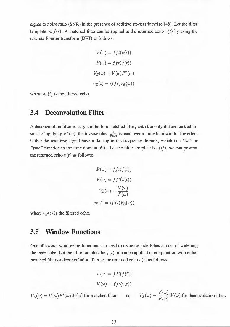
signal to noise ratio (SNR) in the presence of additive stochastic noise [ 48]. Let the filter
template be f ( t). A matched filter can be applied to the returned echo v ( t) by using the
discrete Fourier transform (DFf) as follows:
where vE(t) is the filtered echo.
V(w) = f ft(v(t))
F(w) = fft(f(t))
VE(w) = V(w)F*(w)
VE(t) = ijjt(VE(w))
3.4 Deconvolution Filter
A deconvolution filter is very similar to a matched filter, with the only difference that in
stead of applying F*(w), the inverse filter F(w) is used over a finite bandwidth. The effect
is that the resulting signal have a fiat-top in the frequency domain, which is a "Sa" or
"sine" function in the time domain [ 60]. Let the filter template be f ( t), we can process
the returned echo v(t) as follows:
where vE(t) is the filtered echo.
F(w) = fft(f(t))
V(w) = f jt(v(t))
V(w) VE(w) = F(w)
VE(t) =if ft(VE(w))
3.5 Window Functions
One of several windowing functions can used to decrease side-lobes at cost of widening
the main-lobe. Let the filter template be f(t), it can be applied in conjunction with either
matched filter or deconvolution filter to the returned echo v(t) as follows:
F(w) = fft(f(t))
V(w) = fft(v(t))
VE(w) = V(w)F*(w)W(w) for matched filter or
13
VE(w) = ~~~~ W(w) for deconvolution filter.

where W(w) is the windowing function of choice.
VE(t) = ifft(VE(w))
where vE(t) is the filtered echo.
The implemented windowing functions are Hanning, Hamming and Blackman window
ing functions as shown in Figure 3.2, 3.2, and 3.3.
Frequency Domain
0.1
300 400
Time Domain
500 Samples
600 700
Figure 3.1: Hanning window; W [ k + 1] = 0. 5 ( 1 - cos ( 21r n~ 1 ) ) , k = 0, · · · , n - 1.
Frequency Doma1n
0o~~~~~-7.~~~4o~-=~-=~ Samples
Time Domain
Samples
Figure 3.2: Hamming window; W [k + 1] = 0.54-0.46 cos (21r n~ 1 ) , k = 0, · · · , n- 1.
14

Frequency Domain
Samples
Figure 3.3: Blackman window;
0.08 cos ( 47r n~l) , k = 0, · · · , n- 1.
W[k+l]
15
Time Domain
Samples
0.42 - 0.5cos(27r n~ 1 ) +

Chapter 4
Circuits Simulation and
Implementation
This chapter discusses circuits simulations using SwitcherCAD III@(LTspice) [28] and
implementations of the various blocks shown in Figure 2.2 with improvements and addi
tional circuits built in order to complete the UCT UWB radar design shown in Figure 2.4
and 2.5.
All the measurements were taken with Agilent Infinium 54833A DSO as shown in Figure
4.1. The DSO is capable of sampling 4 GS/sec with 1 GHz bandwidth. This means signals
with more than 1 GHz bandwidth would be band-limited.
Figure 4.1: Agilent Infinium 54833A DSO
16

4.1 PRF Signal Generator
The PRF signal generator is the master clock of the system and triggers the generation
of the transmitted pulses. Figure 4.2 shows a design by [47, 30, 1] which generates a
time-jittered narrow pulse (90% duty cycle) train at the terminal marked "out" in Figure
4.2 with an averaged PRF of 2.4 MHz as in Figure 4.4. It operates by injecting thermal
noise from the left half of the circuit (shown in Figure 4.6) to the right half in Figure 4.2.
The right half of the circuit (3/4 74HC04) is an astable that alone generates a 2.8 MHz
pulse train. Figure 4.3 shows the simulated waveform. Figure 4.5 is the coupling of the
oscillation of the right part of the circuit back into the left part.
Jittering smears the spectral components so that there are no distinct (and easily de
tectable) spectral harmonics. We have, however, opted for using a 50% duty-cycle square
wave signal generator with adjustable frequency to gain greater control of the system. A
PRF of 2.0 MHz was typically used, corresponding to a maximum unambiguous range of
R - c - 3*108m/s - 75 h' h · h ffi · f . d . max - 2*PRF - 2*(2*l06)Hz - m W lC IS more t an SU Clent or Ill OOr testmg.
12 Kolun
12 Kolun
+ l2.2!!F
100 Kolun
100 Kolun
24-pF
3/4-74-HCO.f.
15 Kolun
1 Kolun 1NUt.S
Figure 4.2: The noise modulated pulse generator used in [47, 30, 1].
4.2 Transmitter
The transmitter circuit by [47, 1, 30, 15] reproduced in Figure 4.7 was designed to drive
a balanced dipole antenna. Monolithic base-band pulses are emitted whenever the base
of the transistor in Figure 4. 7 is triggered by the PRF waveform [ 4 7]. The design was
modified to drive an antenna via (unbalanced) coaxial cables as shown in Figure 4.8. This
allowed more freedom in experimenting with available antennas. After some initial ex
perimentation, the original2N5109 transistor (with a gain-bandwidth product of 1.2 GHz)
was replaced with a BFR91A transistor (with a gain-bandwidth product of 6.0 GHz).
17

l.5V v(• QQ9 ~
5.0V
L SV
4.0 V
l .!V
l .OV
2 .5V
2.0V
1.5V
I .OV
) .5V
l .OV "' '-, '-, '-, 'II ',
l.5V 3 3. 4 ,, 33.611' 31.0 p;
J ' · ' ~ ' J 4.6 1U JS.Op' 35.2 )1 $ J S.O p; J5.8 pt
Figure 4.3: The simulated output voltage at node "out" (in Figure 4.2) is plotted as a function of time. The period is approximately 360 ns.
l t . ...................... T ....................... i" ...................... 1' ...................... i ....................... ~~ ...................... i ....................... Tft·~·~· ............... T ........................ r~
~ 1": I!' ................................. fr --, 11r 1 1~1r ~ ...................... · ·y·· ·· · ··· ····· ·· ··· · · · ·····~··········· · ···· ·· ·· ···· T................. ················································ ···; ·························!··· ···················
: j 1 ; : : ................ .... . "f""" """"" " """ "i"""' "' ' ' """ ..... t'"""""' """'""''!""""'"' ..................... .. ............. , ... ................. ··t .............. ......... '!'........ ......... ·+· ................... '
' '
···+ ,.. ., .. ; .... , .... , .... , ... ·r+ ' ... , ' r+•· ' + :·· •·· , .... , ....... , .•. , .. , ·r •·++· . t .. , ... , ... , .• t·+·,·+ ., ··t· ,., .. , ... , ... .
..................... .. t .......................... i ................... ... t" .................... .. .. l" ................................................ ! ........................ t ......................... ! ..................... T ...................... ..
j ~ ................ ~ .. _ .......................... ! ................. ·~ _ ...................... .. .. : ................... ~, ......................... ! ..................... M .............................................. ~ .... .
. ; t l ~ ......................... t... '' ................ y ........ '' .......... ,,' ... '"" .... ! .............. t"'"'" ................ i.·.. ''"t"'""""""'"" ""'i,,: ........... .. ..... "'t' .. , ...... ""'"'.
t
Figure 4.4: The measured output voltage at node "out" (in Figure 4.2) is plotted as a function of time. The period is approximately 420 ns. Vertical (voltage) scale 1.00 VI Offset 2.46V. Horizontal (time) scale 200 ns.
18

3.6V
3.ZV
I I I I
I I I I 1 o I I I
2.w ------- --r-------- ·r-- ------- -------- --r---- -----:----- --- -T -------- ·r --------- r- ------- ·r--- ---- ··1· ------- -·r----- --- -
2 4V _______ ---:----- __ --r------ __ ----------:----------: _____ ---:--- -------~--- __ ----:-- ____ ----:----- __ :----- ____ -: ______ __ 2.ov --------- r---- ---- -!--------- --- ---- ---:------ ---; ----- -- -- ·:- --- ------ r--- ---- ---.--------- ·r--------- r--- -----·:---- -- --- ·
I I ' 1 I I 1 I I I
1.6V ---------1----------:---------- ----------:---------- r---- ----- r-------- -:--------- ·1------- ---:- · ------- ·1·-------- -:----------
I I I I I 1 I I I I
1.2V -- -- -- - - - r- -- ----- ·r---- ----- -------- -·r--- ------:-- ------- T------ ---: --------- r -------- ·r --- ---- ··1·-------- ·r------ ---• I I I 1 I t I I I
o.sv ---~- ... -- ~--- ------ -~--- ------- ------- - - -~-- --- - -- --~-- -------1------- ---~-------- -1-------- --~- --------- ~- -------- -~- ---------: : : : : : : : : :
0.4V ·---- -- - - --;---- ------:---------- ----------:--------- -! ----------:-------- --~-- ------- ~---- ------:----------1-------- --:- --- ------' I I 0 0 I I I I I
! I ~ ~ ~ ~ ~ ~ I
O. OV'+-----T-----r---~r---~,---~-----T-----r-----r-----r-----r----,_--~ 33 .~ 33 .9,.5 33.~ 34.q..s 34.~s 34 .4-Js 34 .EIJs 34 .~ 35.q..s 35.~ 35.4!-Js 35.EtJs 35.9,Js
Figure 4.5: Noise generated from the left-half of the circuit shown in Figure 4.2.
+ . .
····· ·····················-!······· ·· ·················!··························+·········--···············!···················· ······+··························!············· .. ···········+···"''''''''"' '''' '' ''''!·············· .. ····· .. ···+·· ....................... .
. : ! : t i,: ! i I : . : :
......................... t .......................... i"' ....................... ; ......................... r ....................... !' ......................... :--........................ : .................................................... _ ....................... ..
. t . . ........................ .c, ......... . ..... .. ......... ! .......................... + .......................... ; .......................... + ..................... .. ... j ....... .... .......... .. . + ................ .. ........ l_ .......... . ....... . .... ... r,,_ . . . . . .... . . .. ... . .. . ..... .
! ~ l ~
. + ........................ -r ...................... .. ·,_· ..... .. .. .. .......... ... t .......... .. ...................................... J ......................... i" ....................... r ....................... ; .......................... f ........................ .
.. ........ .. ... .. .. . ·-- ·t_·: ··························:··························t,,,',,,_ ...................... ·+-- .................... 1 ........ .. ..... .. .... .. :... .............. : ... " ""t"" " """ " " """"": "' '""""' " ' "' '"""1"""'"""'''"""""
......... ,!••·························.i,_ .......................... ·!····················· """""" " " " " ""+"' " ""'"''""""" !"" " "'""' ' '""""+""'""'"" '"t""""""'''"'"" "!,' ' ' '' ' '' ' ' ' '' ' ' ''' '' ' ''' ' '+'''''''''''''''''"''''' ' '
+
Figure 4.6: The measured noise generated from left-half of the circuit shown in Figure 4.2. Vertical (voltage) scale 500 mV I Offset 1.629V. Horizontal (time) scale 200 ns.
19

+15V
5 I 4- 74-HC04-lpF BA'T!il I .... ' ! , .. 9 ~ 2.2 Kulun
to tlt.e recei ver
~
Figure 4.7: The transmitter used in [47]. .
V2
U4 C4
~~-------~ 74HC04 241>
Figure 4.8: UCT UWB Radar Transmitter
20
68 oJun .. .lA
68 olun
BA'T!il .. t
R14
50
dl pule
ntenna

The master clock is a 50% duty-cycle square wave with PRF of 2.0 MHz (the upper
waveform in Figure 4.11). It triggers the emission of the pulses by the falling edges.
When it is injected into the input labelled "Signal_Generator" in Figure 4.8: during the
non-triggering phase, the circuit is charging capacitor C7 via the loop G->V2->Rl2-
>C7->R13->G; during the triggering phase, capacitor C7 is rapidly discharged via the
loop G->R14->D2->C7->Q4->G. The function of the diode D2 is to prevent capacitor
C7 being charged via the antennas which means unintended emission by the antennas.
The simulated waveform at node C4-R10-U5 is shown in Figure 4.10 while the lower
waveform in Figure 4.11 is captured by the DSO. Since placing the oscilloscope probe
at the node C5-Rll-Q4 (which feeds into the base of the transistor Q4) will affect the
waveform observed, only waveform generated by simulation is available as shown in
Figure 4.12. The simulated pulses emitted at the antenna terminals using the circuits in
Figure 4.7 and Figure 4.8 are shown in Figure 4.13 and Figure 4.15 respectively. The
dipole antenna is simulated using the equivalent SPICE circuit in Figure 4.9 published by
[17].
L1 C9
R17
2
R18
L]~~~---L--------~ 73
Figure 4.9: Equivalent SPICE circuit for a dipole antenna [17].
The simulated pulse shown in Figure 4.15 has a 3dB bandwidth, measured at the point
voltage drops by ~ from the peak value, equal to 1.35GHz. Pulses captured by directly
feeding the transmitter to the oscilloscope with input impedance of son are shown in
Figure 4.14 and 4.16 using 2N5109 and BFR91A transistors respectively. The BFR91A
transistor provided shorter pulses than those generated by the original2N5109 transistor.
The pulses generated by the BFR91A have usable spectral components from DC to 2 GHz
as shown in Figure 4.17 while its measured 3dB bandwidth is l.OGHz. Since the DSO
has only 1 GHz bandwidth, the waveform observed in Figure 4.16 is band-limited by the
scope, i.e. the pulse width and peak height are probably better than displayed.
4.3 Manual Delay Line and Fast Sampler-Averager
Figure 4.18 shows the fast sampler and integrator used in [47, 1, 30, 15]. A delay is
generated according to the RC constant (obtained from the 1 kO fixed resistor in parallel
with the 1 kO variable resistor coupled with the 47pF capacitor to ground) between PIN
21

4 .~·~----.-----.-----~--~----------~~=~2)~--.-----.---~~--~----~-----,
I I I I I ------.-- ~---------- ---------- --------- ~----- --- "f--------- i------- -- - --------- --------- ~----3 .fN
' I ' ' I I I I I I I 1 I I 1
2 .7¥ ---------~--------- ----- . --- --·-r·· -----:------ -- -;-·------- --------- ---------:-·-- ----·--------- ---------
:: • , ••..••••... ··•• ,_. .•..•• T .. · :••···· ••.•••..•.•..••••••• •••••• T ••.•.. r······· •••••.•••. . ' ' . . '
, I I I I
' ' '
-0 ,9{ ' ' --·------,----- -----;- -·-- --
' ' ' ' -1 .9{ ------ - -- ~-- --------:------
- ______ _, __________ ... _____ - ________ .. __________ .. _____ ---·----------' ' ' ' ' ' ' ' ' ' ' ' ' ' -2 .N -----· ---:----------:------- -----. -- ~ - ---------:-- -- ------ . -- ----- ~--- -- -- --- ~--- - -- ~------ -- --
' ' ' ' ' ' ' ' ' ' ' ' ' ' ' ' ' ' ' ' ' ' ' ' ' ' ' ' ' ' ' ' ' ' -3.6\1 ---------,----------·------ -- ---,.----------.---------- --------,------ ---·----------' ' ' ' ' ' ' ' ' ' ' ' ' ' ' ' ' ' ' ' ' ' ' ' -4.1N+-----+-----+-----r------r------;--------r------r------r-------;-------;------+-------l
33.~ 33.9,Js 33.Q.Js 34 .QJs 34 .~ 34 .~ 34.9,Js 34.!\.Js 35 .QJs 35 .21Js 35 .~ 35.~ 35.!\.Js
Figure 4.10: The simulated waveform at node C4-R10-U5.
+ ; t ; : : ···········+······· .................. [ ........... ....... ······+········ .......... ····!··························t···· .................... i······· ................. t·········· .. ····· ······i············""'''''
t .. ....................... ~ ........ '"'"'"""'"!'"""'"' ' "' ......... ~ .......................... ....... ......... ''""'t' ... .. ..... .. ..... .. .... : ......... "'""""'""t'""''"""" """"'l"'"""""""""'
l : ~ + :
t ..................... ... + ........................ 1 ........... ... "'""""!"""'''""""' ..... """"'"""'""""''t ......................... i"""' .. " " "'" ' '"t""" ' '""' .. .... .... . ~......................... • .. ... ................... .
t ····+····l····+····l····t····l ··+····1····+····1····+····1 --·+ +···t····l····+ ·+··+ ···i.'····+ ··1····+--+ --·t·--·1--··+···+·--+ ··!··--+····1····+····1 ·1····+····1····+····>·+····1 ·++···f····l ··+··+···+····
+
. . . t : : : : ···············--········+·----··· ·--------··--r··· .... -------------·t·-- ................. ·:--··-------·-- ·--·····--t----········--· .......... , .......... ··············+··· ..................... !····· .. ·········· ······· +··························
t
; t : : ... ·····················+··························!·············· ··· ·······+··························!··························+·· ·········· ........ .. j .. .. ......... .. .. ... ... ... ......... . . .
1 ~''. : ~ + !
Figure 4.11: The measured waveform at C4-R10-U5 (lower waveform) with reference to the master clock (upper waveform). Vertical (voltage) scale 2.0 V Offset -1.47 V (master clock) I Offset 4.81 V (C4-R10-U5). Horizontal (time) scale 200 ns .
22

1.2V.--------,----.-------,---,----.-----Y("'-raJT-4::!...J -----.----,---------,.---,----,---------,
0 .8V --------- ---- ----- ' ' ---.----------,.---------' ' ' ' ' ' ' ' ' ' ' ' ___ ._ _______ __ ... ________ _ ' ' 0 .4¥ ---------- ---------' ' ' ' ' ' ' ' ' '
o .ov+------;..--~ ' '
-0 .4¥ ---------:----------:-- -------:---------:------ ---!·--------;----------:- ------- ----------o.ev ----------1----------:- -- -----~----- ----~------ --:--------- -t- ---------:-- ------- --------- ~-- ----- -- - -------- -- --------
, I I 0 I I
I I I I I 1
I I I I I
' ' -1 .2-1 -- -------- ~- -- - ----- -:- ---------:----------:-- ------- ---------1------ -- ---------
' ' ' ' ' ' ' ' ' ' -1.6V ------- .. : ----------:-- --- _________ ... __________ , __ ------- ---------·---------- --------' .
' ' ' ' ' ' ' ' ' ' ' ' ' ' -2.[}1 ·----------:---- ------ :-- ·------ ----------:-------.- -;.--------- --------:-- ------- --------- ~- -- ---- -- -------
' < I I 1 I I I
I I I 1
I I I I I I I I . ' -2 .4¥ ------.-- ~-- -- - ---- ·:--- ---- . ' . ' . ------ "'l"-------- -~--- -- ----!------ --- ·:---------- ---------1---------- --------- ----------
' ' ' ' ' ' ' ' ' ' ' ' ' ' ' ' ' ' ' ' ' ' ' ' ' -2.6V+---t---r----;-----r---r-----r----r-----r---r-- - r----r-----1
33.~ 33.~ 33.t;Vs 34 .(1Js 34 .~ 34 .~ 34.~ 34.E\,Js 35 .(1Js 35 .~ 35.4!Js 35.~ 35.E\,Js
Figure 4.12: Wave form at node C5-Rll-Q4 feeding into the base of the transistor Q4.
2 and PIN 3 of the inverter shown in Figure 4. 18 as in [ 4 7]. However, in order to acquire
a complete down-range profile, a variable delay line must be implemented. Our early
prototypes used a fixed capacitor coupled with a variable resistor which enabled operators
to adjust the delay by manually turning the variable resistor.
The fast sampler-averager is comprised of two integrating single-ended samplers [55], i.e.
they sample the RF signals from the antenna terminals and accumulate DC voltages on
the capacitors from sampled signals. It should be noted that several modifications (such
as removing the Vref (virtual ground) and swapping the 4.7 MD resistors as in [47] with a
different value) have been made to it in the UCT implementation in order to provide faster
response time for near real-time operations as shown in Figure 4.19. The inner working
of fast sampler-averager is discussed in section 4.4 and its performance and limitations
are discussed in section 7. 10 of Chapter 7.
4.4 Computer-Controlled Variable Delay Line and Fast
Sampler-Averager
In order to vary the delay with a computer, a computer-controlled variable delay line was
designed as shown in Figure 4.19. It is implemented by using a fixed resistor of 47D
coupled with a varicap diode in the place of the manually adjustable delay line (between
PIN 2 and PIN 3 in Figure 4.18). The capacitance of the varicap diode varies according
to the reverse voltage across it, and for the MV 104 device used, can vary between about
15pF (at 30V) to about to 80pF (at 0.3V). The response is, however, not linear; being
that the capacitance varies quite a lot at the lower voltage and varies very little at voltages
23

30mV
OmV
-30mV
-60mV
-90mV
-120mV
-150mV
·180mV
-210mV
-240mV
-270mV
-300mV
-330mV 0.050110
V(n006)
;--.. I ~ I \ v
\ I \j
0.055110 0.065110 0.075110 0.085110 0.100110
Figure 4.13: Simulated pulse using 2N5109 transistor across 50D load.
t
. . t · · ······· · ······ ·· ·· · ··· · ·• · ········ · ····· · ··· · ······~···· · ····· ······!···"········· ···· ······+·""'''''' ........ ..... , ........................ ~ .. ; ....................... •··· .................... .
+
j j .......................... +················· .. ·······i··························:'········· ···············•·······
···+···+···+···f .. ·+···+····l···+···' +····1· ·+·+···+····1····+····'1"· ......... ..;-"'f'"-!o ........ -t-oo-4...-1"'"""'·· ··+···
........................ -r .. ················•······· ·········+ .. ·····
'\ + ;: • I :
+···\ :/: ., : \ .,. I : i .
.. ·······,···········\Jl·······.:· .····.·········-·::··············: :·.············ : .................... .
........... !······
.......................... +··························~·····
·······················t········ ................ j ••.•••.••. ··············4-····
Figure 4.14: The measured waveform generated by 2N5109. Vertical (voltage) scale 500 mV I Offset 0. Horizontal (time) scale 2 ns.
24

70mV
OmV
-70mV
-140mV
-210mV
·280mV
-350mV
-420mV
-490mV
-S&OmV
~30mV
-700mV 0.0501JS
V(n006)
I ~
0.0551JS 0.06511'1 0.0751JS 0.0801JS 0.0851JS 0.0951JS 0.10011'1
Figure 4.15: Simulated pulse using BFR91A transistor across 500 load . .;.
. . ; j + . j ............... ········-r--························:··························t··················· ·······; ............. ...... ···· ·t· · ······················i········ · ······ ·· ·········~,:::,_ ························!·························-:--························
t ······ · ·········· · ·~···· · ············· · ·······T······· .................... .. ·············f··························l············ ······1·····--···················f···················· ..... .
+ i ~ t
·························-r-········································ ··········:--·······················r······ ···············r······~~··· · · · · · ·· ·· r·· · · · · · ·· ·· ·· · ··· · ····· · ····· ·····················! ·························t··························
-i- {. \ ! ! !-i--"i-~--t--+-i--1~,.._-+-1-'f""!-"P-+-t-+-.......,T-'"1"""'1'"\· I ····t···· l · + · I···· ···: · ··· , . .__,.l.,.,P'"'i· ......_-t-..;..,...t-t""'f--+-c·b-· ...1..-+-t--t'..J
i I : If l ! . !
1 1 r 1 \r ! - r r -r ···t··· .... ·············· ··+···· ····················+················ ....... ··· ···· ············ ······u··········· ········...-························-······················· ·+·················· ····+·························
. : t : ·········· ............. •....... ·················:·················· ······-r-················ ·······i·························l············· ···········:······················ ··-r·· ........... ········-!--··············· . ····+···· ····················
! . + !
Figure 4.16: The measured waveform generated by BFR91A. Vertical (voltage) scale 500 mV I Offset 0. Horizontal (time) scale 2 ns.
25

'!"
t t .. .. ··············· ······• ········ .. ····· · · ··· · · · ·~· ····· · ·· ................ t ....... .... ......... .... ! ......................... l .................. .... "!" ...................... t .. ·· ................... T ........... ··· · · ···· · · ~ · · ..
j ! j .......................... 1 ...................................... -.............. l.... .. . ... .......... ......... y················· ·········;· ··········· ...... .. . ... ~ -- .............. ··········:· ......................... +- ..... .
+ I . .
.......................... t··························i··········· ···············t················· ·······!·················· ········ ·························i············ .. ············t··········--··············i··············· .. ····· .. ··t····· .. ················ ...
.... t .... l .... t .... l .... + ... + .. ·t "+"+"·! .... t .... l .. ...... + .. ·+"+"+ "+"+ " ·i .. .. t .... l .. + " "'""""'"' t ""i"" t ""i"+"·l .... t ... + ... ; .... l .... t .... l ...... ... : .... t .... l ......... l .... ; .... l .. +·+·+ .. ·
J I · : : : · : ~ . ~ l 1 . ........... ................... .................... + .... .................. T ........................ ! ................... =:: .......................... ! ....... ................ + ....................... ! .. ........ ...... ........ t" ....... ..... .. .
l i . . .
: : : : ..i.. : : : '~llurd Figure 4.17: The measured waveform generated by BFR91A with DFT analysis beneath. Vertical (voltage) scale 500 mV I Offset -379 mV. DFT (wattage) scale 20 dBm I Offset -15 dBm. Horizontal (time) scale 50 ns. DFT (frequency) scale 200 MHz I Position 1 GHz.
+5V
o.1 ~-~F T 5 /4-74HC04- "\1
15 pF 6
from tke transmitter in
10 nF
68 olun 4.7 Molun
dipole Vref
~•. _ . . lifie 10 nF -( 4. 7 M olun to ...., DtStruJnentanon 3.Jil p r V
10 Kolun 10 nF
Figure 4.18: The delay line and the fast sampler connected to a balanced dipole antenna used in [ 4 7].
26

close to 30V as shown in the graph in Figure 4.20. The MV104 varicap diode has a typical
diode capacitance temperature coefficient of 280ppm/°C which means the delay may be
affected due to variations of the ambient temperature. This would be discussed further in
section 7.9 of Chapter 7.
A DAC voltage output from the NI-DAQ card is connected to the varicap diode via an
inductor (AC choke) at the point labelled "VI" in Figure 4.19. Voltage V1 is varied
in the range of 0.3V to 10V which provides a capacitance varying from 80pF to 25pF.
Figure 4.21 shows a plot of the reverse voltages across the diode versus delay achieved
for the computer-controlled variable delay line circuit. The delay ranges from 15.82ns
(at 10V) to 93.73ns (at 0.3V) by measuring the phase difference between the input of
U7 (the master clock) and the output of U8 in Figure 4.19. This total delay range t8 =
93. 73ns - 15.82ns = 77.91ns corresponds to the maximum operating range R0 = ~ = 11.68 metres of the radar. The delay was measured using the Agilent Infinium 54833A
oscilloscope.
To lnstrumer.t:af: ion A m
To ln!trume nhl ion Am
R23 C1~
.---~--~ v--~---H~I ---~~-~ 1Ch R14
&I
C1
\r----------11~R4
~&1~~0
Figure 4.19: UCT UWB Radar Delay Line and Fast Sampler-Averager
The fast sampler-averager is triggered by the falling edge of a delayed negatively go
ing pulse at node C14-D5-D2-R24 at the rate of the PRF. To explain the operation of
the fast sampler-averager, each PRI can be decomposed into two phases: triggered (i.e.
charging of capacitor C15 & C1), and non-triggered (i.e. discharging of C15 & C1).
With reference to Figure 4.19, after the transmitted pulse is emitted, the triggered phase
begins according to the delay being set, and it lasts a very short duration determined by
T1 = RsampleC = (Ra II R14 ll R24ll Rl II R4) *C14 = 10[h1.2pF = 12ps where Ra models the antenna load. Therefore, whenever the base of the transistor Q5 is triggered,
a negatively going pulse pulls the node C14-D5-D2-R24 to -5V, which forces those two
Schottky diodes D5 and D2 into conduction mode and produces -4.7V at nodes C15-D5-
27

CL 0..
w () z ~ ()
~ <3 w Cl 0 Cl
-1-
()
100
70 ......... ~ ....... ....
r-.""'
"' 40
...........
~
' ' ' 20
........ ~
'roo.
' ' ' ""'
10 0.3 0.5 1.0 2.0 3.0 5.0 7.0 10 20 30
VR, REVERSE VOLTAGE (VOLTS)
Figure 4.20: Reverse voltage v.s. capacitance of MV104.
10 .-,----,---,----,---,,---,----.---,--~
9
8
~ 6
J 0 > 5 ~ ~ " a: 4
3
X: 15.82 Y: 10
oL---~---L----L---~---L--~----~--~--~--~ 0 10 20 30 40 50
Delay (ns)
Figure 4.21: Voltage vs. Delay
28

R23 and Cl-D2-R2. This, in tum, completes two sub-circuits CIRCUIT! and CIRCUIT2
as shown in Figure 4.22 with their Thevenin equivalent circuits in Figure 4.23.
CRCUrT1
02
CRCUrT2
C15 ~----~~~A~m~e~n~na~
R14
50
C1
10~R4 ~50~ 50
Figure 4.22: Sub-circuits CIRCUIT! and CIRCUIT2.
C15 R1411Ra
CIRCUIT1 ~·· v C1 R111R4
CIRCUIT2 ~·· 501150
v
Figure 4.23: Thevenin equivalent circuits of CIRCUIT I and CIRCUIT2.
In order for the fast sampler-averager to work correctly, it is assumed that voltages of
the returned echoes are always higher than -4.7V which is always the case; being that
voltages of the returned echoes are always in the m V range.
For the triggered phase, capacitor C15 is charged with potential difference between the
antenna terminal and -4.7V as shown in CIRCUIT! above. The current would flow
from the antenna terminal towards -4.7V because the voltages of the returned echoes
are more positive. The time constant for the capacitor to be charged to ~63% full is
T2 = RchargeC = (SOD II SOD) * lOnF = 2SOns. Therefore it takes T2 -7- T1 ~ 20000
pulses to do so. At PRI=500ns, Tcharge = P RI * 20000 = !Oms. This means that if volt
age on the antenna terminal Va increases by !J.v, the charge time constant for the capacitor
is lOms. We can call this the active charge time. Similarly, for CIRCUIT2, capacitor Cl
29

will be charged to -4.7V after the initial active charge time has elapsed because 6.v in this
case is always nil.
The rest of the PRI is the non-triggered phase, the diodes prevent currents from flowing
through them thus they are considered open circuits, and capacitors C 15 and C 1 are dis
charged in the circuits shown in Figure 4.24 with their approximate Thevenin equivalent
circuits in Figure 4.25 for computing capacitor discharge time.
Figure 4.24: Discharging circuits.
R26+R23
100K+10K
R3+R2
100K+10K
C15 R1411Ra
C1 R111R4
C15
~----~~!A~nt~en~n~a~ RU 50
Figure 4.25 : Thevenin equivalent circuits for the discharging circuits in Figure 4.24.
For the discharging circuits, the time constant TDischarge = [R 26 + R23 + ( R Antenna II Rl)] * C l = [lOOkn + lOkn + (son II son)] * lOn F ~ l ms. This means that if Va
decreases by !:lv, the discharge time constant for capacitor CIS is roughly lms. The time
taken is called the passive discharge time. Capacitor C 1 will not be discharged because
there is no voltage difference across it. It will hold -4.7V which was charged during the
triggered phase (active charging phase).
30

Therefore, the voltage fed into the instrumentation amplifier will be -4. 7V + Vc15 ~
-5V + Va(t) and -4.7V for the upper and lower circuits respectively with t being the
delay set corresponding to the range R where R = ~ .
4.5 Post-Sampler Amplifier
In the circuits described in [47], the outputs of the fast sampler-averager in Figure 4.18
were connected to a back-end AC amplifier. It was designed as a motion detecting circuit
for an alarm. A classic 3-op-amp instrumentation amplifier amplifies the difference signal
(i.e. sampled antenna voltages). The resulting signal is then fed into a nulling circuit to
remove effects from the stationary clutter. Lastly it is amplified by the final stage inverting
amplifier. The design by [47] was a single-rail design with a virtual ground that equals
half the supply voltage.
from sampler averager
from sampler averager
+-'V
2/2 LM558
68 Kolun
+5V
2/2 LM558
2/2DB58
Vref O.l~l
Figure 4.26: Post-Sampler Amplifier used in [47].
It is noted that according to [47], the rationale behind using three op-amp's, instead of a
single instrumentation amplifier is due to cost. For our purposes of range profiling, we
have a dual-rail design that uses a single precision instrumentation amplifier (AD620)
with adjustable gain (1 to 1000) set by the variable resistor as shown in Figure 4.27. The
simplified schematic of AD620 is shown in Figure 4.28 reproduced from the data sheet
[2].
Low-pass filters made from the combinations of lMD resistors and lnF capacitors in
31

R3
11
Variable Resistor
AD620
r-----1 RG RGr---i 1n
+VS +15V
1n
-15V -VS REF
Figure 4.27: UCT UWB Post-Sampler Amplifier
R1 R2
RG
12
10k!1
10kfl
>-4~ OUTPUT
10kf!
H..,_-vw---o +IN R4
400!1 ......___. __ -<>_ .JVVV-- -o------..-..... GAIN GAIN
SENSE SENSE
-Vs
Figure 4.28: Simplified Schematic of AD620 reproduced from [2].
32

Figure 4.27 remove all RF components from the sampled signals that are fed into the
instrumentation amplifier. With the values shown in the figure, the cut-off frequency is
f c = 21rkc = 27r*lMe1gfhlnF :::::::: 160Hz. They are also limiting the maximum sweeping
rate which is discussed in section 7.10 of Chapter 7.
33

Chapter 5
System Integration
This section describes aspects the hardware modules that were used to implement the
mono-static and hi-static UWB radar designs depicted in Figures 2.4 and 2.5 and how
they are integrated into a computer system to produce down-range profiles.
5.1 RADAR Circuit
Figure 5.1 is a picture of the UCT UWB radar prototype (mono-static), containing the
short pulse generator, the computer-controlled variable delay line, the integrating single
ended samplers and the low noise instrumentation amplifier. The components were sol
dered onto a PCB of size 7cm by 10 em, with a ground plane on the top surface. The 2.0
MHz PRF signal generator and RF amplifiers were separate modules.
Connected to Varicap Diode
Antenna
Clock Signal In
Figure 5.1: UCT UWB radar prototype (Mono-static)
34

5.2 NI-DAQ Card
The National Instrument Data Acquisition (NI-DAQ) card PCI-MI0-16E-1 (PCI-6070E)
in Figure 5.2 provides an interface between the computer and the radar circuit. It is a 12-
bit, 1.25 MS/s (mega samples per second) input sampling rate, 16-single-ended-analogue
input (or 8-differential-analogue-input), 2-analogue-output at 1.0 MS/s, 8 digital-I/O,
Multifunction DAQ. It provides varying voltages used to slide the range gate shown in
Figure 2.4, while at the same time it also samples the voltage generated by the instrumen
tation amplifier which forms the down-range profile. The voltage range for both I/0 is
±lOY.
According to the Nyquist theorem, if the highest frequency component fH = 2.0 GHz,
then the sample spacing of 2JH = 2{;.t~:~ ) = 0.075m is required in the downrange
profile [60]. For a maximum range of 5 metres, the down-range profile would contain
5/0.075=67 samples. Therefore, if we wish to sweep the whole range every 0.5 second,
we would need sampling rate of at least 134 samples/sec. This is also the minimum
output sampling rate; being that each D/ A output voltage corresponds to a specific range
bin. The NI-DAQ card easily fulfils this requirements. Although the required sampling
rate is merely 134 samples/sec in both I/0, in the experiments conducted, both I/0 were
set to ! AID = fn ;A = 10 KS/s. Setting the IO sampling rate to be identical may simplify
the operation of the hardware simultaneous triggering of both IO.
Figure 5.2: NI-DAQ
35

5.3 Front-End RF Amplifier
A front-end RF amplifier shown in Figure 5.3 which was developed by [59] can be fitted
at the front end prior to the receiver in the hi-static configuration of Figure 2.5 . It utilizes
two stage amplification as shown in Figure 5.4. Its key characteristics are gain of 25dB
at 1.5GHz with noise temperature Te ~ 400K. Figure 5.5 and 5.7 shows its gain versus
frequency range; Fig re 5.6 and 5.8 shows its noise temperature versus frequency range.
The amplifier was not ideal for this application as the gain response was not flat, and
rolled off from about 600 MHz. It did however improve the SNR quite significantly in all
experiments, and could be replaced by a more suitable amplifier module in the future.
Input
Figure 5.3: Front-End RF Amplifier
I 100nF'
""'='"
200R
Figure 5.4: Two-Stage Amplification
36
=!= 100nF
200R
92PF' Output

.40--------------~----~---~ ~ .. .. r ·---:-_......,.._. ...... ~ ,, ... = ~ ... ~~·--·-····· r .... ~ .............. _~-- '!.·w~·-~tl· t· ... ---·'l!"'l!i!!lfH•• ... ""'---.. .. rJ· ""'~flll .......... _;·-·· ... ··1'! .. -···r-.. ···~ ·· ·, ... .. . ,_A •••••.,_- ... ...... , ~!!'lriiPPf •••- ··-- ._ "! .,. ~! ft ,..,, , ..... ..... , .. ...,..IJ !I'f"'ll ..... ., .. --.. •• • •• •••••••~ · ••••r•r-•ao•••••••••••""·"'""'' '"!'"'• -"' : : I ~ . : :
""''.P) -·· U;:o;.o.-·-••.. • • '••• 14W . I ' ., -··iiil. .. oio.l .. lll ~ "'·-·-l\1 .. 1 •• 't'"'"' ... "' W-Wiillflf .. ~ il l •• l""''"'"''"- '!1•!!111
""«; I . • . . - ' .:5() t ................ .. .. ;.,..-.... 111!! ...... :······ .. - .. --., ~ .. ;:. ., •• , .... llj . .. .. .. _ _ ..;~. --. ,. ... ".,.,.·r--· .......... " .. . aJ ---r..._----.~-.--~~-------~-r·~· ~ :(6. lft'l ... tl• r····--·r•..,...ttfi ~~-y--~"' '"'""-'""' .. r·----... ~1rlr~.---~~~r'""",-=-·--~.·"'·- .... -~«> . ~ -:;2-4 •f"'• ;,.;_.,.,_,.:I t•t , ..... ,._:•••p,:- oa.t·-••"'' •••ll!""•r• .... • ...&.~.lf'l•-r •--••••••••rr~•-'" "'_...,. •• _,r··"-~--· ..,, :22 .•• .. un•• ........ . , ........ ~ -... • ... - -!!'111·-·--••i ... ....... ----·•w ........ _ ..... _,.. !!,, ... ,....,._.-." .......... .,,,+•·-..--·•• • ... ,_. =.10_. tl't'il• ,.,._. .... .. - ~--··I ti•'"'- ~~!···~···~·-~·------·· ·~11; .................... ~ .. ..,.-, ....... ~ .. ,. ..... ~ .. L ........ ---~·
~ ... : -1 : .: : 18 ~oit:tk ... "'·!ll-...._t"-,1\•llli.·tttlfii!I!:L~ eese!!!a:toat-~·-.......·-!:.~f'""'"""'"--""~-!~ .... ltf't···--"!·_...,. •• _."".-·""-]"'••.......-.. --. ~~ ~- ±tAll -- ~ -~...,..?~** --·-£--~--r-.~--u.,._...;;-~~-._,. 14 _ _ ...... ~111" 1•·--·~_...........---:··-·---·-~--~ ...... --~ ..... 1 · .• , ...... -·~----...... '4-.. -......... ... .. ~ ....... ,, .... .......,.l_ .... ,.,_ ... _ ll.tlllil.,li • .---.-!IM lll.lliii--.oi·W ""111' 1tf•._.••..-~ · ••r ! ''ff'llll _ _ ,.._.,,,, .. .. ,._.. .... ~ 4 1 1 I I I I
, 0 l'llf'-(lljior-----t!!!!l!l-··11 ...... -r---.... ~ll!llll't··1-·-· ....... ·•lf Ill: ...... :a. ......... ~"!1'11•·-···· · ... ~·· .......... ,_., , r~~·---·-~·14
8. ,.W,i~i----•~tooiol!**•iiil•~ .. ~~~~~-...,."'!'t..:!•-ot•a...• .. •-r.rJ:..--••••ir--.._,, , iirrt ll.., .. ,. .... ... .... t<lllltt : ~ :: - l = ~ ~
6•,.,----~~!"-'""'~ :- ~ .. ..,....-..::--~-~--~ *'t----.....!fl A ~·---~~·· .... ~-~ .... ~~~ ..... ~.f;f"JIIA-~~-·--~--~~o~·--· .. ~ ••••• ,-... --~........ ....... : lllli~ ....... ll!!f .. f"l ••• ,.-.....-.;1!! .... ---~····-~·-·~····"--· .. : • ! : _!_
I l.2
Figure 5.5: Gain vs Frequency Response(Gain in dB)
12 - , I I I ! : .. ~
t !Uaatt•••• '"'ooiiWr i i1 WIIWtali& oiio o IWI I t 01pt1 t~aiiiiUUlo il~llllllllt ~·· -·-- .. W<IIIWI ,_, .,. •••• ., ........ lai! ~W--....... l wPI'IP IIIt••.- · -··
: r ~ : : : • I -:. ~ : : !
"'""-IL";'"'"'W-111_,. : .. ~- ......... - •• :U ... k'l • .--~t---·&.v..,...._..t-a~ .. :§ io:-ll:l"tlt•~fi&fri!i!IH-r-~idool .. .. • le • - •
'•t I ••••wl ......... t .t .. l I fJtot>!.. - ... .. t .. W"I Ill.! •P•••-•••- .. II f!'l-'fii•OII.-, .... .._~ i~~~~~'lfWII-•-.-. .. -J ..... - . ...._I,tll l IWII1•a•-
: : I ~ : : ! I W I llj I I f' I a I I ' • I
""•••• f-•··--"··l!tltlll .... ... ··-··! t 111 •••,.·---·•· •~ nt••••·-- --~.a , ...... ......., .,-f·~---:-···~·•...-• I ~ a ._ tl ~
: . ~ ~ : : -""·-~~!. ---M~-1: ' .-....--..•"r~IUillio.l..~---~~... ~""~
- t ~ ~ : : 1ilf11f .. IIIII"'"'" ' '" ~atiiji"liliiii iiWWI"' ... "' ~-· i·-illl.ltW .. 'I"I'I"Jl!!lfi WWI .... .......... - ...... IIWflf JIIW PP"''•--t! ~lfia;!i,T- .~i-l't
i ! l ~ ; ~ I : i ~ .;
•••••• llllf'lll!llf!l-· - .. ............ 111 ·-·-··· lll llllf'f'lll······'····· ... - ••• --......... ~ ............. ~.~ .... ~ • ,: !1, ! : :: ... "' : • i ~ .. -~-~~ ·-t"_... : --:--~!l'b. eo _ •
- - .......... "'!!!!llllflltii!"'"""-""M• .. ttill• ll11'""'1 .. .._, ...... ,.,...,.- .... . ~ a • I
~ ' J ~ ~ ~ 2 j - ....... l!!!!I!I'W .... ~~ ,. ... ._.r ..... -'fti._~· .... -~~T··il·- ......... _r--........ -..-f!!!!! . ..... i •• ....._.,~.-..... --.........
= _L._ . .. ;; ~ ~~ e : : ~ -1 r---..· .;. •. , .. ___ ~~ -~~, .... __. · :..-.. -~ ............ -.....::~;...... ..... ...,. ..... --...;.~-.... -~ 0 L , •
o 02 Q.4 as na 1 t2 1.4 1.6
Figure 5.6: Noise Figure vs Frequency
37

0
. .!
' F"~( HZ)
Figure 5.7: Gain vs Frequency Response(Gain in ratio)
' -.x:o _ _ . ........,, t-., •• , ...... ____ ........ ..,.__.__..., •••••• _ .... ••• r-•r--.-....... t----·· i ; ~ i .! . r .. "' .. .,
3:X) -----~ ... .. .. .......... .. ~·-····fl......___._ .. __ • .::.. .. ~~.: • ..._...-..-._..,; ~·~-~_..-----........ .. it I ~ t i i !
lOO .. .._ ...... ,.._ ................ - --... ~,." .._-.L-~. r~ .......... L..-- w, ~ i j : _,i i
. ! . j - 3 0o o.2 0.-4 06 OB 1 1.2 1..<4
tip r~(IH%)
Figure 5.8: Noise Figure vs Frequency(Te in Kelvin)
38

5.4 Antennas
Different kinds of antennas were examined. They are bow-tie antennas and grid anten
nas.These were not designed specifically for this project, but were readily available and
offered broadband operation.
5.4.1 Bow-Tie Antennas
Experiments were carried out using bowtie antennas operating in two different frequency
ranges:
• A GPR antenna made by [5] (see Figure 5.9). Its stated operating frequency is 50-
400 MHz, corresponding to a fractional bandwidth off 155%.
• Two twin-bowtie antennas [45], designed to operate in L-band frequency range
between 1 - 2 GHz. These are shown in Figures 5.10 and 5.11. These were built
by an undergraduate thesis student in 2004, who reported the gain vs frequency
characteristic, which we plotted in Figure 5.12 (for the twin-bowtie antenna with a
flare angle smaller than 40°) and Figure 5.13 (for the twin-bowtie antenna with a
flare angle wider than 40°). It is noted that the antennas resonates at 1.53 GHz as
reported by [ 45].
Figure 5.9: GPR Antenna (50- 400 MHz)
39

Figure 5.10: Twin-bowtie Antenna #1 (1 - 2 GHz) with a flare angle smaller than 40°made by [45].
-H!-, ----;':-~--!;------;':-:';-,. ~;----;-;------:';-----;':;-------! r_., tOHrl
Figure 5.12: Plot of measured gain vs. frequency of the twin-bowtie antenna with a flare angle smaller than 40°as measured by [ 45].
40
Figure 5.11: Twin-bowtie Antenna#2 (1 - 2 GHz) with a flare angle wider than 40°made by [45].
4!-, ---;':-~-!;----;':-:';-,.~~--;-;------:';-----:':~ F__.,jOHl)
Figure 5.13: Plot of measured gain vs. frequency of the twin-bowtie antenna with a flare angle wider than 40°as measured by [45].

5.4.2 Grid Antennas
Three different TV grid antennas manufactured by Ellies Electronics were also tested
[9, 10, 11]. Their specifications are shown in Table 5 .1.
Name I Freq. Range (MHz) I 2o/:;f:l I Gain (dB) I H. Beamwidth I -'
Small Grid Aerial 512- 800 43.9% 8- 11 35° Grid Aerial Red I Yellow 512-704 31.6% 12- 14 30°
Grid Aerial 512- 800 43.9% 10- 13 32°
(a) Small Grid Aerial (b) Grid Aerial Red I Yellow (c) Grid Aerial
I l - - ........... ........_., I I - ---- I I -- / il ~ - --_,.. .... .. -- -- 1.1. -... -- j ---.... ....... _. :Ill ....... ,_.... -...._ - - ----- il ~ Jl . 1:: ... .. -- " . ........_.,
~ - Ill .......
"=' • P! - .,.. ~ -...., I II ............ _::::. 1.::: 1,..;;.,.1 ---.... I II --- ,_, • """"' -..... - -..........._, __... -- ,.._ , -- ']! .... ...- II. ........ - l,lllllll - - ,.
-... -- !"\ ..111.: ~ - -...._ ..-
-..... ---.: - • .......... -
Table 5.1: Grid Antennas
41

Chapter 6
Software System
This chapter outlines the software aspects of the UCT UWB radar system including
design, implementati n and operation of the software. The software was built using
MATLAB™Release 14 with the DAQ toolbox running on Windows XP™. An excerpt of
the software code is included in Appendix A. Formula used to convert from sample space
to distance (range) in metres is presented in the example of operating the radar included
in this chapter.
6.1 Software Design
Figure 6.1 shows a block diagram of the software system and interfacing components.
From the block diagram, two sub-systems are within the scope of this section, namely
the Graphical-User-Interface (GUI) and the Digital-Signal-Processing (DSP) unit. The
GUI is responsible of accepting user inputs to control the delay in the radar circuits via
the data-acquisition system and feeding user-defined values to the DSP block. The DSP
is responsible of processing the acquired data with user-defined values, and displaying
results in the Display.
6.2 Software Implementation
A multi-threaded system is needed for displaying the down-range profile in real time.
Fortunately the NI-DAQ card used in this project is capable of not only simultaneous
operations of its inputs and outputs modules; simultaneous triggering (a hardware feature)
of input and output ensures that qata is captured synchronously with varying the output
voltage to control the delay line.
6.2.1 Graphical User Interface
An interface built in MATLAB 's GUI development environment (GUIDE™) is shown in
Figure 6.2. It consist of a main display which displays current range profile data with its
42

PC
User Inputs f"' GUI ~ DSP ~/ v '-- ~0
,r- ~
~7 NI-DAQ
DAC ADC
./
Figure 6.1: Software design.
FFf analysis beneath it.
The following GUI functionality were identified and implemented:
1. User controls:
(a) Start the system.
(b) Stop the system.
(c) Take a background snapshot.
(d) Take a filter snapshot.
(e) Save the current plot displayed.
2. User-defined values:
(a) Sweeping period/rate.
(b) PRF (Pulse-Repetition-Frequency).
/
~
(c) Band of interests- minimum and maximum frequency range.
(d) Display scale -minimum and maximum voltage displayed.
3. User choices:
(a) Display mode.
(b) Filter type.
Display
The controls for these features can be seen on the right-hand side of Figure 6.2.
43

IU 0 .005 -
4.5
3.5
2.5
2
1.5
0.5
0 -
0.45
0.4
0.35
0.3
0.25
0.2
0.15
0.1
0.05
0
Slort I Slop
Background II Filter
Sweeping Period aa··c
) \ 500 1000 1500 2000 2500 3000 3500 4000 4500 5000
120 140 160 180 200 220 240 260
Figure 6.2: Software Interface
PRF MHI
Display Mode
Faer Type ~- -:=-t '--· ---"----..:..
Lowerfreq . ~ MHz
tiglef f req. ~ MHZ
Q SayCheese!
6.2.2 Digital Signal Processing
Corresponding to different displaying modes and window filter type (for range side-lobes
suppression discussed in Chapter 3) selectable by the user, the following options are pro
vided:
1. Display mode:
(a) Raw- unprocessed captured data.
(b) Background - snapshot taken with a stationary scene.
(c) Difference - current captured data minus the background.
(d) Filter- snapshot taken with a point-like target with background removed.
(e) Matched- current captured data with background removed and passed through
a matched filter.
(f) Deconvolved - current captured data with background removed and decon
volved with the filter snapshot.
(g) Envelope - current captured data with background removed and passed through
an envelope detector.
2. Filter type:
(a) Hanning window.
(b) Hamming window.
(c) Blackman window.
44

6.3 Software Operation
Operating the UCT UWB radar system involves:
1. Initial set-up:
The user must choose the sweep period Tsweep (seconds per sweep) prior to opera
tion. The default value is 0.5 second per sweep.
2. Background clutter acquisition:
The user sets up a stationary scene in front of the radar, then clicks on Background
button. Ten down-range profiles are averaged to generate the source of background
removal.
3. Point-target calibration:
(a) The user places a calibration target (several reflectors are shown in Table 7.1
of Chapter 7) in the scene at approximately 1.0 m in front of the radar, then
clicks on Filter button to capture the scene's response with the background
removed to generate the source of filtering.
(b) Alternatively, the user can place the antennas about 2.0 m apart facing each
other, then click on the Filter button to capture a perfect system response (as
would be received from a perfect point target at range 1.0 m).
4. Real-time displaying of the down-range profile:
The user can activate a real-time display of the down-range profile by clicking on
the Start button. It will display different information according to the display mode
chosen below.
5. Choosing the display mode:
(a) Raw: In this mode, the down-range profile including the background clutter
is displayed.
(b) Background: Display a static down-range profile of the background clutter
taken in Step 2.
(c) Difference: Also known as background removal. It displays the current down
range profile with the background removed.
(d) Filter: Display a static down-range profile of the point-target response recorded
in Step 3.
(e) Matched: In this mode, the matched filter is applied to the current down-range
profile.
(f) Deconvolved: The deconvolution filter is applied to the current down-range
profile.
45

6.
7.
Choosing the filter type:
(a) None.
(b) Hanning.
(c) Hamming.
(d) Blackman.
Setting the band of interests:
The user can choose a frequency band of interest by adjusting the Lower Fre
quency and Higher Frequency values.
6.3.1 Distance Conversion and an Example
In the following example, distance (range) has been converted from sample space to me
tres by using the formula R = n * ~ = __!!:.._ * C*77·91ns where n denotes the
T sweep*fA / D 2 5000 2
number of the n1h samples. A series of signal processing techniques [60] is applied to the
raw returned echo to produce a set of results which can be usefully interpreted. The series
is outlined as follows :
1. Figure 6.3 shows a background snapshot taken without any targets in the scene.
This background will be subtracted in all the processes that follow.
2. Figure 6.4 shows a filter snapshot f ( t) taken when a calibration target (plate reflec
tor "Small Grid" in Table 7.1) was placed at 1.0 min front of the antennas (with
background removed) . The length of the captured filter response is set to 1000
samples in time (2.34 min space). The rest of the samples are zero-padded.
3. Figure 6.5 shows the echo v(t) (with background removed) from the same calibra
tion target, which now is used as the intended target.
4. Figure 6.6 shows the echo v(t) being filtered by matched filter with band of interest
{3 = 1.0 rv 2.0 GHz.
5. Figure 6.7 shows the echo v(t) being filtered by deconvolution filter with band of
interest f3.
6. The final result in Figure 6.8 is obtained by applying a Hanning window to Figure
6.7.
46

5
4
3
2
~ Q)
0 rn ~ 0
> -1
-2
-3
-4
-5 0 2 3 4 5
Distance (m)
Figure 6.3: Background snapshot
-2
-3
-4
-~~------~--------~--------~------~~------~
Distance (m)
Figure 6.4: Echo from calibration target used to create deconvolution filter
47

5
4
3
2
~ Q)
0 en
"' 0 > -1
-2
-3
-4
-5 0 3 4 5
Distance (m)
Figure 6.5 : Unprocessed echo from a plate reflector
10
9
8
7
> 6
g Q) 5 en ~ 0 > 4
3
2
0 2 3 4 5
Distance (m)
Figure 6.6: Match filtered with no windowing applied
48

5' _§_
3
2.5
2
~ 1.5 "' ~
l 0.8
Q)
C">
2 ~ 0.6
0.4
0.2
0
0
0
2 3 4 5 Distance (m)
Figure 6.7: Deconvolution filtered with no windowing applied
2 3 4 5 Distance (m)
Figure 6.8: Deconvolved and Hanning windowed
49

Chapter 7
Results and Performance
This chapter discusses the performance of the UCT UWB radar system for range profiling.
First the circuit performance is characterised, particularly achievable pulse width and
bandwidth. Second the radiated bandwidth is discussed by characterizing the antennas
used. Third the processed bandwidth, in other words the portion of the received bandwidth
which is processed, and is directly related to the resolution presented to the users. Fourth
the power radiated is discussed, centred on peak power and averaged power; followed by
discussion on miniaturization of the circuit. Following that, the laboratory environment
where the experiments took place is surveyed. Next various targets were placed in the
scene to produce down-range profiles to demonstrate the capabilities of the system for de
tecting metal objects with and without obstacles. According to those down-range profiles,
signal-to-noise ratios at different ranges are calculated and discussed. Last the maximum
sweep rate achievabl and maximum speed detectable by the system are discussed.
7.1 Achievable Pulse Bandwidth
The achievable pulse bandwidth of the UCT UWB radar system is estimated and verified
by simulation using Switcher CAD III, direct measurements using the Agilent Infinium
54833A digital oscilloscope.
• The simulated pulse shown in Figure 4.15 has a 3dB bandwidth equal to 1.35GHz.
• Pulses captured by directly feeding the transmitter to the oscilloscope with input
impedance of son shown in Figure 4.16 have usable spectral components from DC
to 2 GHz as shown in Figure 4.17 while its measured 3dB bandwidth is 1.0GHz.
7.2 Limitations of Simple Antenna Structures
The performance is primarily determined by the antenna used because the antennas act
as bandpass filters in the system; provided the pulse generated has spectral components
50

which cover the operating frequency band of the antenna. Testing was carried out with
the various antennas described in section 5.4.
According to [5], the bowtie antenna functions over 50-400MHz band which is equivalent
to 350MHz bandwidth. Therefore a 3dB range resolution of 42.86cm is expected.
With Ellies UHF grid antennas with a stated bandwidth of 288MHz, the best 3dB range
resolution achievable is 53.08cm.
For UCT twin-bowtie antennas, whose operating frequency range is l.OGHz-2.0GHz, the
3dB range resolution is 15cm since its bandwidth is 1GHz.
7.3 Processed Bandwidth
The processed bandwidth is the difference of the higher frequency f H and lower frequency
h values entered in the GUI discussed in section 6.2.1 of Chapter 6. It is common to set
those values within the operating frequency range of the antennas used because of the
gain provided by the antennas used. However, this processed bandwidth can be larger
than the designed operating frequency range of the antennas used.
By observing the down-range profile in Figure 6.7, a 3dB bandwidth of 917MHz is cal
culated. After applying Hanning window, the resulted down-range profile in Figure 6.8
has a 3dB bandwidth of 558MHz. This decrease of bandwidth due to the windowing is
expected.
7.4 Peak Power Radiated
In theory, the peak instantaneous power may be computed from P = Yj , where V0 is
the peak voltage driving an ideal antenna of with an input resistance of R Ohms. With
a supply voltage of 15V, Vo ~ 14. 7V (the voltage to which the output 1.2 pf capacitor
is charged, minus diode drop), and assuming an ideal antenna impedance of R = 500,
the calculated peak transmitting power is 4.32W. In practice, this peak value would be
diminished as a result of finite switching time, component losses and current limiting by
the output transistor.
7 .4.1 Simulation
Although in theory the peak transmitting power can be as large as 4.32W, because of the
current limiting nature of the components built into the transistor model, the simulated
peak power is merely 8.0m W calculated by observing the peak value in Figure 7 .1 .
51

8.8m v
8.0m v
7.2m v
6.4m V'-
5.6m v
4.8m v
4.0m
3.2m v
2.4m v
1.6m v
0.8m v
v O.Om 0.0601J1
(V(n006)"V(n006)V49 9
r\ I \ I ---
I I I I I
I
I I
I lJ "" 0.062 ... 0.063 ... 0.064 ... 0.0651'1 0.0661'1 0.0671'1 0.0681'1 0.0691'1
Figure 7.1: Instantaneous power of the simulated waveform of Figure 4.15.
7 .4.2 Oscilloscope Measurement
0.0701'1
The Agilent Infinium 54833A digital oscilloscope was used to observe the output voltage
waveform, as developed across a son load. The resulting peak power of 31 .9m W was
observed from the peak value in Figure 7 .2, again well below the theoretical maximum
of 4.32W. It is however stressed that this is not a reliable method of measurement, as the
rated bandwidth of the oscilloscope is only 1.0 GHz, which will limit the rise and fall
time, and hence the observed peak is expected to be lower that which in fact is developed
across a SOn load. Fourier analysis of the echoes captured by the prototype UWB radar
showed significant spectral components beyond 2.0 GHz.
7.5 Averaged Power Radiated
The total power per pulse is calculated by integrating the area underneath the instanta
neous power curve shown in Figure 7.2. The integration yields a value of 16.75pJ per
pulse. With PRF of 2.0 MHz, the averaged power is then 16.75pJ * 2.0MHz = 33.5J..LW.
Hence the title of this dissertation - "A Micropower Ultra- Wide band RADAR Profiling
System."
It is stressed, howev r, that this is not an accurate measure of the power because of the
bandwidth limitation of the oscilloscope.
52

35,---,----,----.----,----,----.----.----,----.----.
30
25
~ 20
§.
I Q. 15
10
0 - 5 -4 -3
) ~A~ -2 - 1 0 3 4
Time (ns)
Figure 7.2: Instantaneous power across 500 of the pulse waveform captured in Figure 4.16. P(t) = v~? .
7.6 Limitation of Indoor Measurements
Experiments were carried out in an laboratory shown in Figure 7.3. The twin-bowtie
antennas can be seen aimed at a grid reflector. There exists a back wall at approximately
4.7 metres from the antennas and in front of the back wall, there are some furniture at
3.7 metres. They are all part of the background clutter. As one can notice in Figure 6.8,
at 3.7 metres there exist some low-profiled targets ; please note that these are not noise,
but the effect due to the background clutter. The reason for this phenomenon is because
the background clutter forms part of the background snapshot, therefore, when there is a
target present, the background clutter will "appear" since the target now shields part of
it. In the figures presented in section 7.7.2, as the target moves away from the antenna,
this background clutter will gradually "sink" into the background as a target positioned
further away shields a smaller portion of the background.
7.7 Capability for Detecting Metal Objects
The metal objects we tested are listed in Table 7 .1.
Experiments were carried out using the the UCT UWB radar prototype in hi-static mode
(as in Figure 2.5) with the UCT twin-bowtie antennas (shown in Figure 7.3). The antenna
with the "V-shaped" elements (aligned at 40°) (as shown in Figure 5.11, and positioned
on the left in Figure 7.3) was used for transmitting, while the other antenna with elements
53

with a flare angle smaller than 40 I Photo RCS Shape I Dimensions (mm)
Fan Mesh Circle 440 in Diameter
Small Grid Rectangle 550x390
Large Grid Rectangle 830x485
Ball 55 in Radius
Corner Reflector Pyramid 500 per Side
Table 7.1: Metal Objects Tested
54

Figure 7.3: Experiment Setup
aligned in parallel (as in Figure 5.10, and positioned on the right in Figure 7.3) were used
for receiving. A metal sheet was placed between the two antennas to minimize direct
coupling between the TX and RX antennas, which may swamp the returned echoes.
The following results were obtained from a "Small Grid" as the target in various config
urations with deconvolution filter set to 1-2 GHz and Hanning window applied. They
are separated into two groups; one group has no RF amplifier (discussed in section 5.3)
attached but is attached with a higher gain setting for the back-end amplifier (discussed in
section 4.26); the other group has the RF amplifier attached with a lower gain setting for
the back-end amplifier. The down-range profiles without RF amplification have not been
converted to metres using the formula presented in section 6.3.1 to provide a comparison
with the down-range profile with RF amplification which has been converted to metres .
It should be noted that the "Small Grid" target is only visible up to a range of about 1 m
without a RF amplifier. If D denotes the maximum dimension of the antenna aperture,
and ). is the wavelength of the highest frequency component (2.0 GHz), then the far
field distance Rfar - f ield ;::: 2f 2
= 2 (~:~~)
2
;::: 0.833m. With the RF amplifier attached,
the antennas are thus operating in their far-fields because targets are now visible up to 5
metres within the laboratory.
7.7.1 Performance Without RF Amplifier
Figure 7.4 shows the echo from the "Small Grid" target at 50cm. Figure 7.5 represents the
target at 80cm. This experiment was done using bow-tie antenna shown in Figure 5.10.
These targets are visible up to only 1 metre (sample number 1000) in range. Returned
echoes from targets further than 1 metre away rapidly diminish below the noise floor.
55

0.01 .--------,------r-------,-------.---------,
0.009
0.008
0.007
0.006
0.005
0.004
0.003
0.002
0.001
5000
Figure 7.4: Target at 50cm without RF amplifier.X-axis: Sample (spans from -2.33m to 9.35m).Y-axis: Voltage (V).
0.009
0.008
0.007
0.006
0.005
0.004
0.003
0.002
0.001
1000 2000 3000 4000 5000
Figure 7.5: Target at 80cm without RF amplifier.X-axis: Sample (spans from -2.33m to 9.35m).Y-axis: Voltage (V).
56

7.7.2 Performance With RF Amplifier
We have much better results with the RF amplifier attached. Available range is estimated
to be increased by 10 folds. The following figures are obtained using the twin bow-tie
antennas with deconvolution filter set to 1 - 2 GHz range and Hanning window applied.
Figure 7.6 shows a scene without targets. Figure 7.7 shows the target at l.Om, Figure 7.8
shows the target at 1.5m, Figure 7.9 shows it at 2.0m and Figure 7.10 shows the target at
2.5m, while a target at 3.0m is shown in Figure 7.11.
Multiple targets are shown in Figure 7.12 with the "Ball" target positioned at 1 metre and
the "Small Grid" target positioned at 2.5 metres in the scene.
3.5,-----.------,-------.-------.------,
3
2.5
> 2 g Q)
t:r>
"' ~ 1.5
0.5
0 0 2 3
Distance (m)
Figure 7.6: No Target with RF amplifier.
7.8 Detection through Obstacles
4 5
This sections represents results from detecting hidden targets being shielded by obstacles
such as a partition or a cement wall. It is unfortunate that "seeing-through-wall" was only
possible to pick up targets standing right next to the wall. Thus the results from were not
recorded.
57

3
2.5
> 2 g Q)
rn ~ ~ 1.5
0.5
0
3
2.5
> 2 g Q)
rn
"' ~ 1.5
0.5
0
0
0
2 3 4 5 Distance (m)
Figure 7.7: Target at l.Om with RF amplifier.
2 3 4 5 Distance (m)
Figure 7.8: Target at 1.5m with RF amplifier.
58

3
2.5
> 2 5 Q)
Ol
"' ~ 1.5
0.5
0
3
2.5
> 2 5 Q)
Ol
"' ~ 1.5
0.5
0
0
0
2 3 4 5 Distance (m)
Figure 7.9: Target at 2.0m with RF amplifier.
2 3 4 5 Distance (m)
Figure 7.10: Target at 2.5m with RF amplifier.
59

3.5.---------.---------.---------,----------,---------,
3
2.5
> 2 g Q)
Ol
"' ~ 1.5
Q)
Ol
"'
0.5
0
3
2.5
~ 1.5
0.5
0
0
0
2 3 4 5 Distance (m)
Figure 7.11: Target at 3.0m with RF amplifier.
2 3 4 5 Distance (m)
Figure 7.12: Targets at l.Om and 2.5m with RF amplifier.
60

7.8.1 Detection through Wooden Partition
After point-target filter- snapshot is taken, a partition with dimensions 120cm (W) * 2cm
(B) * 180cm (H) was placed l.Om in front of the antenna, shown in Figure 7.13. After
wards, a background snapshot was taken again with the partition in it thus includes the
effect of the partition. Since now the partition is part of the background, it won't be shown
on the down-range profile anymore.
The following down-range profiles were taken with a "Small Grid" as the target in the
scene. Figure 7.14 shows a target 50cm behind the partition, which is 1.5m from the
antennas. Figure 7.15, 7.16, and 7.17 show the target at 2.0m, 2.5m, and 3.0m.
Q)
Ol
"'
1.2
~ 0.6
0.4
0.2
2 3 4 5 Distance (m)
Figure 7.13: Partition at l.Om.
The signal levels from these targets has been decreased due to the partition placed in the
scene. By comparing peak values from down-range profiles in section 7.7.2 at different
ranges and peak values shown in the down-range profiles in this section, the decrease
percentage is tabulated in Table 7 .2.
I Range (m) I Peak Volt w/o Partition v1 (mV) I Peak Volt w/ Partition v2 (mV) I Ratio ~ (%) I 1.5 1.35 1.26 93.1 2.0 1.28 0.801 62.5 2.5 0.747 0.704 94.3 3.0 0.425 0.338 79.5
Table 7.2: Decrease due to the placement of the partition.
61

1 .4~--------.---------.----------.---------.--------~
Q)
en
"'
1.2
~ 0.6
0.4
0.2
2 3 4 5 Distance (m)
Figure 7.14: Target at 1.5m. (The partition located at l .Om is not visible after background subtraction.)
Q)
en
"'
1.2
~ 0.6
0.4
0.2
0 0 2 3 4 5
Distance (m)
Figure 7.15: Target at 2.0m. (The partition located at l .Om is not visible after background subtraction.)
62

1 .4~--------~--------~--------.---------~--------~
1.2
I o.s Q)
~ Ol
"' ~ 0.6
0.4
0.2
3 4 5 Distance (m)
Figure 7.16: Target at 2.5m. (The partition located at 1.0m is not visible after background subtraction.)
1.4~--------~--------~--------.---------~--------~
Q)
Ol
"'
1.2
~ 0.6
0.4
0.2
0 0 2 3 4 5
Distance (m)
Figure 7.17: Target at 3.0m. (The partition located at 1.0m is not visible after background subtraction.)
63

This decrease is due to the attenuation introduced by the partition. The ratio is not a
constant value due to inaccurate measurements.
7 .8.2 Detection through Cement Wall
To achieve through-wall detection, a procedure similar to section 7 .8.1 was carried out, the
only difference being that instead of placing a wooden partition in front of the antennas,
the antennas were mounted against a cement wall 9" (23cm) thick to detect movements
in the adjacent room. In this instance the "Large Grid" target was used. It was observed
that through wall attenuation was significantly higher than for the previously described
case of the wooden partition. Targets were only visible next to the 9" wall. It is expected
that with increased transmitted power, a useful range of several metres should be possible.
The non portability of the present prototype prevented further tests on different walls.
7.9 Noise Performance
There are different sources of the noise in the system:
1. Thermal noise from the scene.
2. Thermal noise induced by the front-end RF amplifier.
3. Thermal noise induced by the post-sampler amplifier.
4. Residual background clutter due to drifts in the timing circuit.
5. ND quantization error.
With no target in the scene, 10 down-range profiles were captured and their highest RMS
value is 4.2807 p, V which is the highest noise power from the combination of all the above
sources. Using measurements presented in section 7.7.2, the complete-system's worst
signal-to-noise ratios can be estimated at different ranges with targets at those ranges.
Table 7.3 tabulates re ults from ranges of 1.0, 1.5, 2.0, 2.5, 3.0 metres.
I Range (m) I Noise n (p,V) I Signal v (mV) I SNR=10log10 ~~ (dB) j
1.0 4.28 3.28 57.7 1.5 4.28 1.35 50.0 2.0 4.28 1.28 49.5 2.5 4.28 0.747 44.8 3.0 4.28 0.425 39.9
Table 7.3: Signal-to-Noise ratio at different ranges.
64

Item 4 is mainly because of the capacitance variation due to temperature change of the
MV104 varicap diode discussed in section 4.4. Its diode capacitance temperature co
efficient is 280ppmfOC, thus if the ambient temperature changes in the range of ±5°C
(.0.c = 10°C) during the course of the experiment, then the delay generated by the delay
line may drift up to 0.28%, i.e. 14 samples, or 0.22ns, or 3cm. This and the fact that the
background snapshot's magnitude is significantly larger than those of the returned echoes
(comparing Figure 6.3 and 6.5) results in residual background clutter in the down-range
profiles.
7.10 Achievable Maximum Sweeping Rate and Maximum
Speed Detectable
The maximum sweeping rate achievable ! max is related to various factors:
• Nyquist criterion - the highest frequency component fH of the band of interest
determines the size of range bin cell of the system is R/J = 2/H.
• Some limitations are imposed by the operational conditions, e.g. maximum un
ambiguous range Rmax• pulse-repetition-frequency P RF, maximum/desirable de
tectable range R8, minimum number of range bins N according to Nyquist theorem.
• Some limitations are imposed by the circuitry (component-bounded), e.g. largest of
the various time constants mentioned in Chapter 4 r = max { T 1 , T2 , · · · } . They are
active charge time Tc harge = 10ms, and passive discharge time TDischarge = 1ms
of the fast sampler-averager mentioned in section 4.4, and cut-off frequency f c =
160Hz of the post-sampler amplifier mentioned in section 4.5.
• Some limitations are imposed by the hardware design, e.g. maximum delay-line
range achievable.
• Some limitations are bounded by the hardware modules that interconnects the oper
ational blocks of the system, i.e. NI-DAQ's maximum samples/second Smax• 12-bit
maximum resolution, and hardware drivers.
• Some limitations are imposed by the software (programming-bounded), e.g. max
imum refresh rate of the display loop CJmax combined with the blocking call to
capture data.
A typical scenario is as follows:
• The highest frequency component fH = 2.0GHz =? R¢ = 2jH = 7.5cm per range
bin.
65

f - 2 OMH R - E!:.E..HL - c 1 - 75 e PRF- . z =} max - 2 - 2 * fPRF - m.
• Maximum detectable range R8 = 5m =? N = Ji! = 67 range bins.
Since Te harge > TDischarge • using the worst case estimate, we would have to assume that
at each range bin's position, the single-ended integrating samplers need at least r = r eharge = lOms to reach ~ 63% of the steady state; for N = 67 range bins, it needs
r * N = 0.5s per sweep. This means DC voltages at the output terminals of the fast
sampler-average are changing at a maximum rate of 67 levels per 0.5 second which is
equivalent to say that !De = 134Hz. Since !De :::; f c , the maximum sweeping rate
!max = 2Hz in this case. If the target is moving, the maximum speed it travels at without
introducing aliasing can be determined by calculating ! max * R<P = 0.15m/ s.
If all conditions stand, except the desired detectable range is now 2.5m, then the number
of range bins are halved. One quickly concludes that the maximum sweeping rate !max is
now 4H z without examining all limitations. In this case, because fc = 160Hz, the DC
voltage can only change at a rate up to 160 levels per second without being distorted, the
maximum sweeping rate is 3.2H z imposed by the low-pass filters deployed at the input
terminals of the post-sampler amplifier. Thus the maximum speed detectable in this case
is 0.24m/s.
66

Chapter 8
Conclusions and Future Work
This dissertation presented the design and implementation of a UWB Short-Range radar
with result showing its performance for short range object detection. It has also provided
a literature survey for UWB radar technology, discussion of the signal processing tech
niques utilized, and design of the graphical user interface.
Judging from the outcomes of the experiments conducted, UWB-pulse technology is a
promising candidate for short-range radar applications because of its simplicity, low-cost
and good performance. It is also evidential that a miniature circuit design is possible
because of the low component count, and the use of digital hardware. Furthermore, it has
the advantage of having a low probability of interception and detection if the master clock
is jittered.
Future work should include
• implementation of a portable battery powered version for use with a laptop.
• improvement of detection range and range resolution:
- the transmitter stage could be improved to provide increased peak power, and
a narrower pulse.
- the existing front-end RF amplifier should be replaced by broader bandwidth,
low noise, high gain amplifier designed for pulse amplification (having a flat
ter response across the band of interest.
• development of a multi-channel receiver to allow experimentation with an antenna
array.
• development of suitable broadband antennas, and particularly to be used in a broad
band array.
• development of software/algorithms to produce 2-D and 3-D images from array
data.
• testing of array-based imaging capability in applications like through wall imaging.
67

Appendix A
Software Source Code
The following is an excerpt from the MATLAB source code responsible for the displaying
loop. It triggers simultaneous 1/0 of the NI-DAQ card to capture the data and process the
captured data accordingly to display the down-range profiles in real-time.
Program A.l: localShowData.m % --- Executes while startButton is activated . function localShowData(hObject , event)
3 handles= get (hObject , 'UserData ' ) ; 4 putdata(handles . ao , [handles . y ' )) ;
start(handles . ai) ; 6 start (handles . ao) ; 1 trigger(handles . ao) ; 8 data = get data (handles . ai) ; 9 Q round ( 4 0 0 I 2 5 ) ;
10 L round (str2double(get( handles . edit2 ,' String ' ))/Q) ; 11 M round (str2double (get (handles . edit3 , ' String ' )) /Q ) ; 12
13 Nx = length (data) ; 14 data(Nx+l : 2*NX) = 0 ; 1s handles.background(Nx+l : 2*NX) 0 ; 16 handles .filter (Nx+l : 2*NX) = 0 ; 11 Nx = length (data) ; 18 L 2 * L ; 19 M = 2 * M; 20
21 V_Max str2double(get( handl es . V_ Max_ Value ,' String ' )) ; 22 V_Min str2double (get (handl es . V_ Mi n_ Value ,' String ' )) ; n contents= get (handl es .modeMenu ,' String ' ) ; ~ switch contents{ get (handl es . modeMenu ,' Value ' )} ~ case ' Raw ' H data = data ; n plot (handles . profilel , data ); 28 V = axis (handles . profilel) ; axis (handles . profilel , [V(l) Nx
/ 2 V_ Min V_ Max)) ; 29 plot( handles.profile2 , abs (fft (data ) )) ; m V = axis (handles . profile2) ; axis (handles . profile2 , [round (L
31
32
-2 0 ) round (M+20 ) 0 V(4))) ; % V = axis (handles .profile2) ; axis (handles .profile2, [V(l)
Nx/ 2 0 V ( 4)]) ;
n case ' Background Snapshot ' M data = handles .background; ~ plot (handles . p r o f i l el , data) ; 36 V = axis (handles . profilel) ; axis( handles . profi l el , [V(l) Nx
/2 V_ Min V_Ma x) );
68

37
38
plot (handles.profile2, abs (fft (data))); V = axis (handles.profile2); axis (handles.profile2, [round (L
-20) round(M+20) 0 V(4)]); 39 % V = axis (handles.profile2); axis (handles.profile2, [V(l)
Nx/2 V(3) V(4)]); 40
41 case 'Difference' 42 data = data - handles.background; 43 plot (handles.profilel, data); 44 V = axis (handles . profilel) ; axis (handles.profilel, [V(l) Nx
/2 V_Min V_Max]) ; 45 plot (handles.profile2, abs(fft (data))); % V = axis( handles.profile2) ; axis( handles.profile2 , [round (L
-20) round (M+20) 0 V(4)]); 47 % V = axis (handles .profile2); axis (handles .profile2, [V ( 1)
Nx/2/5 V(3) V(4)]); 48
~ case 'Filter Snapshot' ~ data = handles. filter; 51 plot (handles . profilel, data); 52 V = axis (handles.profilel); axis (handles . profilel , [V(l) Nx
/2 V_Min V_Max]); 53 plot (handles.profile2 , abs (fft (data))); 54 V = axis (handles . profile2); axis (handles.profile2, [V(l) Nx
/2 V(3) V(4)]);
55
~ case 'Matched' 57 data = data - handles.background; 9 DATA= fft (data); w FILTER= fft (handles .filter); ~ DATA(l:L) = 0 ; 61 DATA(M+l:Nx)= 0 ; ~ FILTER(l:L) = 0; M FILTER(M+l:Nx)= 0; M FILTER=FILTER/ sum (sqrt(abs(FILTER) . A2)) ; 65 wBox = get (handles.windowBox,'String'); 66 switch wBox{ get (handles . windowBox, 'Value')} ~ case 'Hanning' 68 DATA(L+l:M) DATA(L+l:M) . *hann(M-L); 69
70
71
72
73
74
75
76
77
78
79
80
81
end
case 'Hamming' DATA(L+l:M)
case 'Blackman' DATA (L+l : M)
DATA(L+l:M) .*hamming(M-L);
DATA(L+l:M) .*blackman(M-L);
data ifft (DATA.* COnj (FILTER)); data circshift(data , handles.Fstart); plot (handles.profilel, abs (data)); V = axis (handles.profilel); axis( handles . profilel , [V(l) Nx
/2 V_Min V_Max]); plot (handles.profile2 , abs(fft (data))); V = axis (handles.profile2); axis (handles . profile2 , [round (L
-20) round (M+20) 0 V(4)]); data= abs (data);
n case 'Deconvolved ' 83 data = data - handles.background; M DATA= fft (data); e FILTER= fft (handles. filter ); H FILTER= 1./FILTER; ~ DATA(l:L) = 0; u DATA(M+l:Nx)= 0; n FILTER(l:L) = 0; ~ FILTER(M+l:Nx)= 0; 91 FILTER=FILTER/sum(sqrt(abs (FILTER) . A2)) ; 92 wBox = get (handles . windowBox,'String') ;
69

93
94
95
96
97
98
99
100
101
102
103
104
105
106
switch wBox{ get (handles.windowBox ,'Value')} case 'Hanning'
end
DATA(L+1:M) DATA(L+1 : M) .*hann(M-L) ; case ' Hamming'
DATA (L+1 :M) case 'Blackman '
DATA (L+1 : M)
DATA(L+1:M) . *hamming(M-L) ;
DATA(L+1:M) . *blackman(M-L);
data ifft (DATA.*FILTER); data circshift(data, handles . Fstart); plot (handles . profile1 , abs (data)) ; V = axis (handles . profile1) ; axis (handles.profile1, [V(1) Nx
/2 V_Min V_Max)) ; plot (handles . profile2 , abs (fft (data))) ; V = axis (handles . profile2) ; axis (handles . profile2, [round (L
-2 0 ) round (M+20) 0 V(4))) ; 101 data = abs (data) ; 1w case ' Envelope' 1w data = data - handles.background; 110 DATA = fft (data) ; 111 DATA (Nx/2+1: Nx) = 0 ; 112 wBox = get (handles . windowBox , ' String' ) ; 113 switch wBox{ get (handles . windowBox, ' Value ' )} 114
115
116
117
118
119
120
121
122
123
124
125
126
127
end data
case 'Hanning' DATA(L+1 : M)
case ' Hamming' DATA (L+1 :M)
case ' Blackman' DATA (L+1 :M)
ifft (DATA);
DATA(L+1 : M) .*hann(M-L);
DATA(L+1 : M) .*hamming(M-L);
DATA(L+1:M) . *blackman(M-L) ;
plot (handles . profile1, abs (data)); V = a x is (handles.profile1) ; axis (handles . profile1, [V(1) Nx
/2 V_Min V_Max )) ; plot (handles . profile2, abs (fft (data))) ; V = a x is (handles . profile2) ; axis (handles . profile2 , [round (L
-20) round (M+20) 0 V (4))) ; % V = axis (handles .profile2) ; axis (handles .profile2, [V ( 1)
Nx / 2 V(3) V(4)] ) ; 128 data = abs (data) ; 129 end 130
131 cheese = get (handles . say_cheese , ' Value ' ) ; 132 if (cheese == 1) 1n set (handles . say_cheese ,' Va lue ' ,O) ; ~~ AxesRect = get (handles . profile1, ' position ' ); 135 figure ; 136 plot (data) ; 137 V = axis () ; axis ([V(1) Nx/2 V(3) V(4))) ; 138 end
70

Bibliography
[1] Micropower impulse radar. Science & Technology Review, pages 16-27, Janu
ary/February 1996.
[2] Analog Devices, Inc. AD620 Low Cost, Low Power, Instrumentation Amplifier, rev.
e edition, 1999.
[3] L. Astanin and A. Kostylev. Ultrawideband Radar Measurements: Analysis and
Processing (Radar, Sonar, Navigation and Avionics Series) . Institution of Electrical
Engineers, 1997.
[4] T. W. Barrett. Performance prediction and modeling. In J. D. Taylor, editor, INTRO
DUCTION TO ULTRA -WIDEBAND RADAR SYSTEMS, chapter 12, pages 609-656.
CRC Press, Inc, 1995.
[5] M. Birch. Development of a cavity backed bowtie antenna with dielectric matching
for ground penetrating radar. Master's thesis, University of Stellenbosch, September
2001 .
[6] T. Carlberg. Analysis of uwb (ultra wideband) for indoor geolocation. Master's
thesis, Chalmers University of Technology, 2000.
[7] Y.-M. A. Chang and A. J. Wilkinson. Investigation of uwb-pulse technology for
short-range radar applications. Technical report, University of Cape Town, Septem
ber 2005.
[8] J. Collins. Hospital gets ultra-wideband rfid. RFID Journal, August 2004.
[9] Ellies. Grid Aerial.
[10] Ellies. Grid Aerial Red I Yellow.
[11] E11ies. Small Grid Aerial.
[12] FCC. First report and order: In the matter of revision of part 15 of the commission's
rules regarding ultra-wideband transmission systems. Technical Report 02-48, April
2002.
71

[13] B. C. Flores and J. Reberto Vasquez. Compression of wideband returns from over
spread targets. In J.D. Taylor, editor, ULTRA-WIDEBAND RADAR TECHNOLOGY,
chapter 5, pages 135-153. CRC Press LLC, 2001.
[14] P. R. Foster, J. D. Halsey, and M. G. M. Hussain. Ultra-wideband antenna tech
nology. In J.D. Taylor, editor, INTRODUCTION TO ULTRA- WIDEBAND RADAR
SYSTEMS, chapter 5, pages 145-286. CRC Press, Inc, 1995.
[15] L. Fullerton. Time domain radio transmission system. US Patent, 1990. US Patent
4979186.
[16] A.-L. Germond, E. Pottier, and J. Saillard. Bistatic radar polarimetry theory. In J.D.
Taylor, editor, ULTRA-WIDEBAND RADAR TECHNOLOGY, chapter 14, pages
379-414. CRC Press LLC, 2001.
[17] J. F. M. Gerrits, A. A. Hutter, J. Ayadi, and J. R. farserotu. Modelling and simulation
of a dipole antenna for uwb applications using equivalent spice circuits. In IEEE
IWUWBS, 2003.
[18] G. S. Gill. Fourier series-based waveform generation and signal processing in uwb
radar. In J.D. 'I ylor, editor, ULTRA- WIDEBAND RADAR TECHNOLOGY, chap
ter 10, pages 291-302. CRC Press LLC, 2001.
[19] G. S. Gill. High-resolution step-frequency radar. In J. D. Taylor, editor, ULTRA
WIDEBAND RADAR TECHNOLOGY, chapter 11 , pages 303-328. CRC Press LLC,
2001.
[20] H. F. Harmuth. Transmitter signature and target signature of radar signals. In J. D.
Taylor, editor, INTRODUCTION TO ULTRA-WIDEBAND RADAR SYSTEMS, chap
ter 8, pages 435-456. CRC Press, Inc, 1995.
[21] J. Harold F. Engler. Technical issues in ultra-wideband radar systems. In J. D. Taylor,
editor, INTROD UCTION TO ULTRA-WIDEBAND RADAR SYSTEMS, chapter 2,
pages 11-50. CRC Press, Inc, 1995.
[22] I. I. Immoreev. Improved signal detection in uwb radars. In J. D. Taylor, editor,
ULTRA-WIDEBAND RADAR TECHNOLOGY, chapter 2, pages 21-46. CRC Press
LLC, 2001.
[23] I. I. Immoreev. Main features of uwb radars and differences from common narrow
band radars. In J.D. Taylor, editor, ULTRA-WIDEBAND RADAR TECHNOLOGY,
chapter 1, pages 1-19. CRC Press LLC, 2001.
[24] I. I. Immoreev and D. V. Fedotov. Ultra wideband radar systems: Advantages and
disadvantages. In IEEE Conference on Ultra Wideband Systems and Technologies.
IEEE, 2002.
72

[25] R. B. James and J. B. Mendola. Ultra-wideband technology for intelligent trans
port systems. In J.D. Taylor, editor, ULTRA-WIDEBAND RADAR TECHNOLOGY,
chapter 7, pages 165-179. CRC Press LLC, 2001.
[26] A. F. Kardo-Sysoev. New power semiconductor devices for generation of nano
and subnanosecond pulses. In J. D. Taylor, editor, ULTRA-WIDEBAND RADAR
TECHNOLOGY, chapter 9, pages 205-290. CRC Press LLC, 2001.
[27] S. Kingsley and S. Quegan. UNDERSTANDING RADAR SYSTEMS. SciTech Pub
lishing, Inc., 1999.
[28] LTC. SwitcherCAD Ill. Linear Technology Corporation, 2005.
[29] V. Z. Marmarelis, D. Sheby, E. C. Kisenwether, and T. A. Erdley. High-order signal
processing for ultra-wideband radar signals. In J. D. Taylor, editor, INTRODUC
TION TO ULTRA- WIDEBAND RADAR SYSTEMS, chapter 11, pages 579-608. CRC
Press, Inc, 1995.
[30] T. McEwan. Uwb radar motion sensor. US Patent, 1994. US Patent 5361070.
[31] N. J. Mohamed. High-resolution ultra-wideband radars. In J. D. Taylor, editor,
ULTRA-WIDEBAND RADAR TECHNOLOGY, chapter 3, pages 47-74. CRC Press
LLC, 2001.
[32] J. Mosquera and M. Isasa. Uwb resistively loaded sensor design. In IGARSS, vol
ume 7, pages 4232-4234. IEEE, July 2003.
[33] R. M. Narayanan, Y. Xu, P. D. Hoffmeyer, and J. 0. Curtis. Design, performance,
and applicaitons of a coherent uwb random noise radar. In J. D. Taylor, edi
tor, ULTRA-WIDEBAND RADAR TECHNOLOGY, chapter 8, pages 181-203. CRC
Press LLC, 2001.
[34] W. C. Nunnally, R.N. Edwards, and D. V. Giri. Direct radiating systems. In J.D.
Taylor, editor, INTRODUCTION TO ULTRA-WIDEBAND RADAR SYSTEMS, chap
ter 6, pages 287-324. CRC Press, Inc, 1995.
[35] D. Platts, 0. S. F. Zucker, and I. A. Mcintyre. Transmitters. In J. D. Taylor, edi
tor, INTRODUCTION TO ULTRA-WIDEBAND RADAR SYSTEMS, chapter 4, pages
109-144. CRC Press, Inc, 1995.
[36] M. Rangaswamy and T. K. Sarkar. Analytical techniques for ultra-wideband sig
nals. In J. D. Tylor, editor, INTRODUCTION TO ULTRA- WIDEBAND RADAR
SYSTEMS, chapter 3, pages 51-108. CRC Press, Inc, 1995.
[37] R. Roussel-Dupre' and T. W. Barrett. Propagation and energy transfer. In J. D.
Taylor, editor, INTRODUCTION TO ULTRA- WIDEBAND RADAR SYSTEMS, chap
ter 7, pages 325-434. CRC Press, Inc, 1995.
73

[38] J. Sachs, M. Rossberg, P. Rauschenbach, P. Peyerl, and J. Friedrich. Integrated
uwb radar circuit for base band applications from de to 5 GHz. In German Radar
Symposium GRS, pages 231-236, Berlin, Germany, October 2000.
[39] T. Sakamoto and T. Sato. An estimation algorithm of target location and scattered
waveforms for uwb pulse radar systems. IEICE Transactions on Communications,
E87-B(6):(in press), 2004.
[ 40] T. Sakamoto and T. Sato. A target shape estimation algorithm for pulse radar systems
based on boundary scattering transform. IEICE Transactions on Communications,
E87-B(5): 1357-1365, 2004.
[41] H. G. Schantz. A brief history of uwb antennas. In IEEE UWBST, 2003.
[42] H. G. Schantz. Introduction to uwb antennas. In IEEE UWBST, 2003.
[43] H. G. Schantz. Uwb magnetic antennas. In IEEE APS/URSI, 2003.
[44] C. E. Shannon. A mathematical theory of communication. Bell System Technical
Journal, 27:379-423,623-656, July, October 1948.
[45] L. N. Shuuya. Design and construction of a twin bowtie antenna for the frequency
range 1-2 gigahertz. October 2004.
[46] K. Siwiak. Ultra-wide band radio: Introducing a new technology. IEEE VTS 53rd,
2, 2001.
[47] E. M. Staderini. Everything you always wanted to know about uwb radar: a prac
tical introduction to the ultra wide band technology. OSEE (Online Symposium for
Electronics Engineers), December 2001.
[48] F. G. Strernler. Introduction to Communication Systems. Prentice Hall , 3rd edition,
1990.
[49] J. D. Taylor, editor. Introduction to Ultra-Wideband Radar Systems. CRC Press
LLC, 1995.
[50] J. D. Taylor. Ultra-wideband radar overview. In J.D. Taylor, editor, INTRODUC
TION TO ULTRA-WIDEBAND RADAR SYSTEMS, chapter 1, pages 1-10. CRC
Press, Inc, 1995.
[51] J. D. Taylor. Ultra-wideband radar capactity demonstrations. In J. D. Taylor, editor,
ULTRA-WIDEBAND RADAR TECHNOLOGY, chapter 13, pages 343-377. CRC
Press LLC, 2001.
[52] J. D. Taylor. Ultra-wideband radar receivers. In J. D. Taylor, editor, ULTRA
WIDEBAND RADAR TECHNOLOGY, chapter 4, pages 75-133. CRC Press LLC,
2001 .
74

[53] J.D. Taylor, editor. Ultra-wideband Radar Technology. CRC Press LLC, 2001.
[54] J.D. Taylor and E. C. Kisenwether. Ultra-wideband radar receivers. In J.D. Taylor,
editor, INTRODUCTION TO ULTRA-WIDEBAND RADAR SYSTEMS, chapter 10,
pages 491-578. CRC Press, Inc, 1995.
[55] J. D. Taylor and T. E. McEwan. The micropower impulse radar. In J. D. Taylor,
editor, ULTRA-WIDEBAND RADAR TECHNOLOGY, chapter 6, pages 155-164.
CRC Press LLC, 2001.
[56] Time Domain Corporation. RadarVision2i: Introducing the Second Generation
Through- Wall Motion Detection Radar for Enhanced Tactical Entry.
[57] L. Ulander, H. Hellsten, and J.D. Taylor. The carabas ii vhf synthetic aperture radar.
In J. D. Taylor, editor, ULTRA-WIDEBAND RADAR TECHNOLOGY, chapter 12,
pages 329-342. CRC Press LLC, 2001.
[58] M. L. VanBlaricum. Radar cross section and target scattering. In J. D. Taylor,
editor, INTRODUCTION TO ULTRA-WIDEBAND RADAR SYSTEMS, chapter 9,
pages 457-490. CRC Press, Inc, 1995.
[59] A. J. Wilkinson. Design, construction and performance of a microwave radiometer.
November 1989.
[60] A. J. Wilkinson. Notes on radar signal processing: Fundamentals, June 2002.
[61] A. J. Wilkinson and Y.-M. A. Chang. Proposal: Investigation of uwb-pulse technol
ogy for short-range radar applications, February 2004.
75