a modeling method of press-pack igbt from chip- level to
TRANSCRIPT

A Modeling Method of Press-Pack IGBT from Chip-level to Module-level
Shuai Sun1, Meiting Cui1, Zhongyuan Chen1, Xiaodong Luo2, Jinyuan Li1 and Huipeng Ren1 1Global energy interconnection research institute co. Ltd., Changping District, Beijing102209, China
2State Grid Jincheng Electric Power Supply Company, Jincheng, Shanxi Province 033000, China
Abstract—In press-pack IGBT the currents flowing through paralleled chips are not consistent due to the packaging structure, chip difference, uneven stress distribution and so on. The maximum current overshoot and maximum junction temperature of the internal paralleled chips determine the limitation of the device's application. A hierarchical modeling method based on the geometry structure of press-pack IGBT is proposed in this paper, and a relatively more accurate device model is established, which provides a reliable and practical modeling method for analyzing electrical characteristics of internal branches under different operating conditions. First of all, according to the data sheet or test results, the chip behavior model is built by Saber software; Secondly, parameter extracting software is used to extract the packaging parasitic parameters and the equivalent circuit network is established; Finally, considering the application environment of press-pack IGBT, a nonlinear resistor is introduced to simulate the piezoresistive effect of a semiconductor and the change of component contact resistance caused by stress. The comparison with test data shows that the model is in good agreement with the test results in key parameters and has high precision. Simulation and test results prove the validity of the model and the feasibility of the modeling method.
Keywords—insulated gate bipolar transistor(IGBT); press-pack IGBT(PPI); model; parasitic parameter; paralleled operation
I. INTRODUCTION
Press-pack IGBT (PPI) is very suitable for high power applications such as electric locomotive traction and large current pulse generator, due to the advantages of the high voltage, large current, low control power, high switching speed, the double-plate heat dissipation and so on. In addition, PPI has the characteristics of short circuit failure, especially suitable for redundant design, so PPI is also an ideal device for high voltage direct current (HVDC) [1]. It is of great significance to establish a practical and accurate IGBT model for the the electrical performance optimization of the device and the safe and reliable operation of the equipment.
Common IGBT modeling software includes Matlab, PSCAD, Saber and so on. The output models of these mature commercial software (modeling tools) have high accuracy and precision. But for chips, discrete devices and modules, the IGBT model in these modeling tools can only be researched as a whole. If the users want to study internal electrical properties, such as the current of each chip in the module, this model can't achieve.
The internal chips in PPI are paralleled, and its failure mode
is short circuit failure, as a result, the limit characteristics of a single chip, such as the maximum current overshoot and maximum junction temperature, determine the limit of the device's application. Due to the factors such as packaging structure, chip difference and uneven stress distribution, the current distribution of the paralleled IGBT chips is inconsistent. Specifically, the dynamic and static non-uniform current characteristics of each chip inside the module are shown as follows.
Differences in the parameters among the chips can lead to the differences of the switching transient and static shunt characteristics of the chips.
Inconsistent packaging parasitic parameters will lead to uneven current distribution of paralleled chips in the switching transient. Mutual inductance between each chip branch can lead to inconsistent chip switching current. The internal gate PCB layout which has considerable asymmetry, leads to various parameters of the chip driving circuit.
Each chip in PPI is under not completely consistent stress. Due to piezoresistive effect of a semiconductor and the influence of stress on the contact resistance, the resistivity difference of each branch affects switching and static current distribution of the chips.
Therefore, the research on the device needs to establish a more precise and hierarchical model based on the differences of chips, structural characteristics and application environment. The user can fully understand the electrical characteristics of the internal branch in the module under different operating conditions so as to optimize the electrical characteristics of the module and predict the safety of the module. In fact, the significance of modeling and simulation is that the parameter measurement is difficult or even impossible. In most cases, it is difficult to measure the current of each branch in PPI, which makes the accurate modeling and simulation more necessary and meaningful.
In this paper, a 3300V/1500A PPI is adopted. Firstly, Saber software is adopted to establish the behavior model of IGBT chip by using the curve fitting method. Secondly, parameter extracting software is adopted to extract the resistance and inductance matrix of each branch circuit of each chip and PCB of the gate drive circuit and the equivalent circuit network is established. Finally, a nonlinear resistor is introduced to simulate the piezoresistive effect of a semiconductor and the change of component contact resistance caused by stress. In
3rd International Conference on Electrical, Automation and Mechanical Engineering (EAME 2018)
Copyright © 2018, the Authors. Published by Atlantis Press. This is an open access article under the CC BY-NC license (http://creativecommons.org/licenses/by-nc/4.0/).
Advances in Engineering Research, volume 127
115
this paper, a double pulse experimental circuit is used to verify the model and the validity of the model and the feasibility of the modeling method is proved by comparing the key indicators.
II. EQUIVALENT CIRCUIT BASED ON MODULE STRUCTURE
A. Basic Structure of PPI
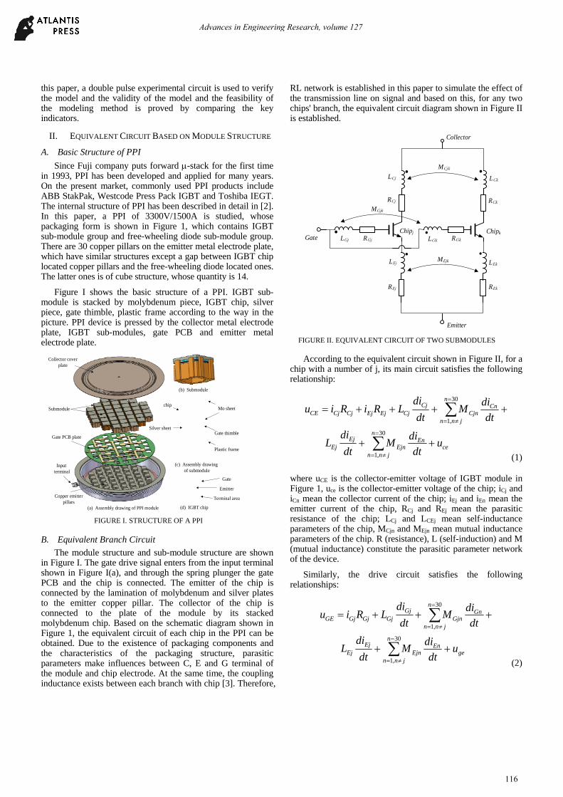
Since Fuji company puts forward -stack for the first time in 1993, PPI has been developed and applied for many years. On the present market, commonly used PPI products include ABB StakPak, Westcode Press Pack IGBT and Toshiba IEGT. The internal structure of PPI has been described in detail in [2]. In this paper, a PPI of 3300V/1500A is studied, whose packaging form is shown in Figure 1, which contains IGBT sub-module group and free-wheeling diode sub-module group. There are 30 copper pillars on the emitter metal electrode plate, which have similar structures except a gap between IGBT chip located copper pillars and the free-wheeling diode located ones. The latter ones is of cube structure, whose quantity is 14.
Figure I shows the basic structure of a PPI. IGBT sub-module is stacked by molybdenum piece, IGBT chip, silver piece, gate thimble, plastic frame according to the way in the picture. PPI device is pressed by the collector metal electrode plate, IGBT sub-modules, gate PCB and emitter metal electrode plate.
(a) Assembly drawing of PPI module
(b) Submodule
(d) IGBT chip
Submodule
Collector cover plate
Gate PCB plate
Copper emitter pillars
Input terminal
Mo sheetchip
Silver sheetGate thimble
Plastic frame
(c) Assembly drawing of submodule
Gate
Emitter
Terminal area
FIGURE I. STRUCTURE OF A PPI
B. Equivalent Branch Circuit
The module structure and sub-module structure are shown in Figure I. The gate drive signal enters from the input terminal shown in Figure I(a), and through the spring plunger the gate PCB and the chip is connected. The emitter of the chip is connected by the lamination of molybdenum and silver plates to the emitter copper pillar. The collector of the chip is connected to the plate of the module by its stacked molybdenum chip. Based on the schematic diagram shown in Figure 1, the equivalent circuit of each chip in the PPI can be obtained. Due to the existence of packaging components and the characteristics of the packaging structure, parasitic parameters make influences between C, E and G terminal of the module and chip electrode. At the same time, the coupling inductance exists between each branch with chip [3]. Therefore,
RL network is established in this paper to simulate the effect of the transmission line on signal and based on this, for any two chips' branch, the equivalent circuit diagram shown in Figure II is established.
LCj LCk
RCj RCk
LEj
REj
LEk
REk
Collector
Emitter
Gate RGj RGkLGj LGk
MEjk
MCjk
MGjk
ChipkChipj
FIGURE II. EQUIVALENT CIRCUIT OF TWO SUBMODULES
According to the equivalent circuit shown in Figure II, for a chip with a number of j, its main circuit satisfies the following relationship:
ce
Enn
jnnEjn
EjEj
Cnn
jnnCjn
CjCjEjEjCjCjCE
udt
diM
dt
diL
dt
diM
dt
diLRiRiu
30
,1
30
,1
(1)
where uCE is the collector-emitter voltage of IGBT module in Figure 1, uce is the collector-emitter voltage of the chip; iCj and iCn mean the collector current of the chip; iEj and iEn mean the emitter current of the chip, RCj and REj mean the parasitic resistance of the chip; LCj and LCEj mean self-inductance parameters of the chip, MCjn and MEjn mean mutual inductance parameters of the chip. R (resistance), L (self-induction) and M (mutual inductance) constitute the parasitic parameter network of the device.
Similarly, the drive circuit satisfies the following relationships:
ge
Enn
jnnEjn
EjEj
Gnn
jnnGjn
GjGjGjGjGE
udt
diM
dt
diL
dt
diM
dt
diLRiu
30
,1
30
,1
(2)
Advances in Engineering Research, volume 127
116
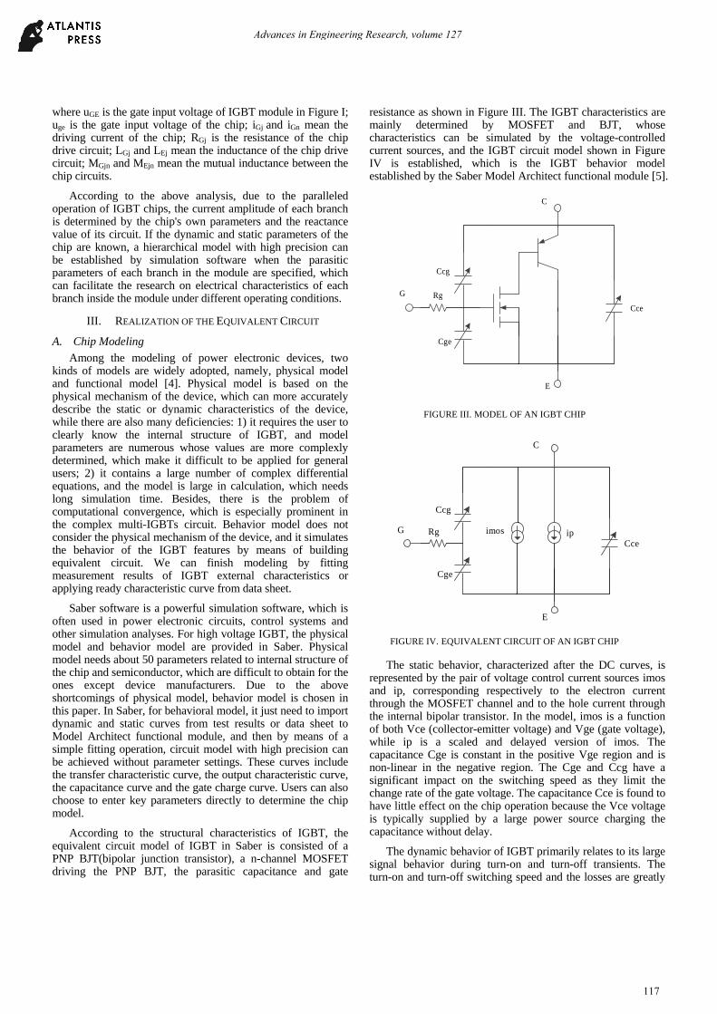
where uGE is the gate input voltage of IGBT module in Figure I; uge is the gate input voltage of the chip; iGj and iGn mean the driving current of the chip; RGj is the resistance of the chip drive circuit; LGj and LEj mean the inductance of the chip drive circuit; MGjn and MEjn mean the mutual inductance between the chip circuits.
According to the above analysis, due to the paralleled operation of IGBT chips, the current amplitude of each branch is determined by the chip's own parameters and the reactance value of its circuit. If the dynamic and static parameters of the chip are known, a hierarchical model with high precision can be established by simulation software when the parasitic parameters of each branch in the module are specified, which can facilitate the research on electrical characteristics of each branch inside the module under different operating conditions.
III. REALIZATION OF THE EQUIVALENT CIRCUIT
A. Chip Modeling
Among the modeling of power electronic devices, two kinds of models are widely adopted, namely, physical model and functional model [4]. Physical model is based on the physical mechanism of the device, which can more accurately describe the static or dynamic characteristics of the device, while there are also many deficiencies: 1) it requires the user to clearly know the internal structure of IGBT, and model parameters are numerous whose values are more complexly determined, which make it difficult to be applied for general users; 2) it contains a large number of complex differential equations, and the model is large in calculation, which needs long simulation time. Besides, there is the problem of computational convergence, which is especially prominent in the complex multi-IGBTs circuit. Behavior model does not consider the physical mechanism of the device, and it simulates the behavior of the IGBT features by means of building equivalent circuit. We can finish modeling by fitting measurement results of IGBT external characteristics or applying ready characteristic curve from data sheet.
Saber software is a powerful simulation software, which is often used in power electronic circuits, control systems and other simulation analyses. For high voltage IGBT, the physical model and behavior model are provided in Saber. Physical model needs about 50 parameters related to internal structure of the chip and semiconductor, which are difficult to obtain for the ones except device manufacturers. Due to the above shortcomings of physical model, behavior model is chosen in this paper. In Saber, for behavioral model, it just need to import dynamic and static curves from test results or data sheet to Model Architect functional module, and then by means of a simple fitting operation, circuit model with high precision can be achieved without parameter settings. These curves include the transfer characteristic curve, the output characteristic curve, the capacitance curve and the gate charge curve. Users can also choose to enter key parameters directly to determine the chip model.
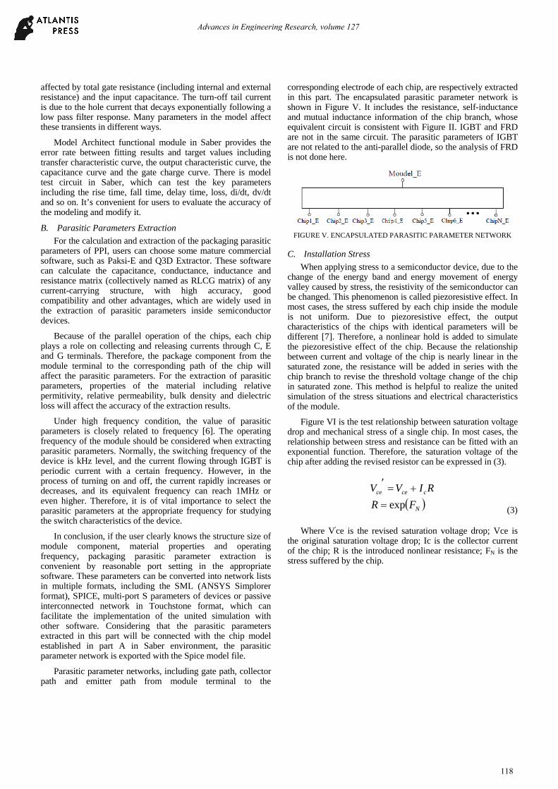
According to the structural characteristics of IGBT, the equivalent circuit model of IGBT in Saber is consisted of a PNP BJT(bipolar junction transistor), a n-channel MOSFET driving the PNP BJT, the parasitic capacitance and gate
resistance as shown in Figure III. The IGBT characteristics are mainly determined by MOSFET and BJT, whose characteristics can be simulated by the voltage-controlled current sources, and the IGBT circuit model shown in Figure IV is established, which is the IGBT behavior model established by the Saber Model Architect functional module [5].
G
E
C
Rg
Cge
Ccg
Cce
FIGURE III. MODEL OF AN IGBT CHIP
G
E
C
Rg
Cge
Ccg
Cceimos ip
FIGURE IV. EQUIVALENT CIRCUIT OF AN IGBT CHIP
The static behavior, characterized after the DC curves, is represented by the pair of voltage control current sources imos and ip, corresponding respectively to the electron current through the MOSFET channel and to the hole current through the internal bipolar transistor. In the model, imos is a function of both Vce (collector-emitter voltage) and Vge (gate voltage), while ip is a scaled and delayed version of imos. The capacitance Cge is constant in the positive Vge region and is non-linear in the negative region. The Cge and Ccg have a significant impact on the switching speed as they limit the change rate of the gate voltage. The capacitance Cce is found to have little effect on the chip operation because the Vce voltage is typically supplied by a large power source charging the capacitance without delay.
The dynamic behavior of IGBT primarily relates to its large signal behavior during turn-on and turn-off transients. The turn-on and turn-off switching speed and the losses are greatly
Advances in Engineering Research, volume 127
117
affected by total gate resistance (including internal and external resistance) and the input capacitance. The turn-off tail current is due to the hole current that decays exponentially following a low pass filter response. Many parameters in the model affect these transients in different ways.
Model Architect functional module in Saber provides the error rate between fitting results and target values including transfer characteristic curve, the output characteristic curve, the capacitance curve and the gate charge curve. There is model test circuit in Saber, which can test the key parameters including the rise time, fall time, delay time, loss, di/dt, dv/dt and so on. It’s convenient for users to evaluate the accuracy of the modeling and modify it.
B. Parasitic Parameters Extraction
For the calculation and extraction of the packaging parasitic parameters of PPI, users can choose some mature commercial software, such as Paksi-E and Q3D Extractor. These software can calculate the capacitance, conductance, inductance and resistance matrix (collectively named as RLCG matrix) of any current-carrying structure, with high accuracy, good compatibility and other advantages, which are widely used in the extraction of parasitic parameters inside semiconductor devices.
Because of the parallel operation of the chips, each chip plays a role on collecting and releasing currents through C, E and G terminals. Therefore, the package component from the module terminal to the corresponding path of the chip will affect the parasitic parameters. For the extraction of parasitic parameters, properties of the material including relative permitivity, relative permeability, bulk density and dielectric loss will affect the accuracy of the extraction results.
Under high frequency condition, the value of parasitic parameters is closely related to frequency [6]. The operating frequency of the module should be considered when extracting parasitic parameters. Normally, the switching frequency of the device is kHz level, and the current flowing through IGBT is periodic current with a certain frequency. However, in the process of turning on and off, the current rapidly increases or decreases, and its equivalent frequency can reach 1MHz or even higher. Therefore, it is of vital importance to select the parasitic parameters at the appropriate frequency for studying the switch characteristics of the device.
In conclusion, if the user clearly knows the structure size of module component, material properties and operating frequency, packaging parasitic parameter extraction is convenient by reasonable port setting in the appropriate software. These parameters can be converted into network lists in multiple formats, including the SML (ANSYS Simplorer format), SPICE, multi-port S parameters of devices or passive interconnected network in Touchstone format, which can facilitate the implementation of the united simulation with other software. Considering that the parasitic parameters extracted in this part will be connected with the chip model established in part A in Saber environment, the parasitic parameter network is exported with the Spice model file.
Parasitic parameter networks, including gate path, collector path and emitter path from module terminal to the
corresponding electrode of each chip, are respectively extracted in this part. The encapsulated parasitic parameter network is shown in Figure V. It includes the resistance, self-inductance and mutual inductance information of the chip branch, whose equivalent circuit is consistent with Figure II. IGBT and FRD are not in the same circuit. The parasitic parameters of IGBT are not related to the anti-parallel diode, so the analysis of FRD is not done here.
FIGURE V. ENCAPSULATED PARASITIC PARAMETER NETWORK
C. Installation Stress
When applying stress to a semiconductor device, due to the change of the energy band and energy movement of energy valley caused by stress, the resistivity of the semiconductor can be changed. This phenomenon is called piezoresistive effect. In most cases, the stress suffered by each chip inside the module is not uniform. Due to piezoresistive effect, the output characteristics of the chips with identical parameters will be different [7]. Therefore, a nonlinear hold is added to simulate the piezoresistive effect of the chip. Because the relationship between current and voltage of the chip is nearly linear in the saturated zone, the resistance will be added in series with the chip branch to revise the threshold voltage change of the chip in saturated zone. This method is helpful to realize the united simulation of the stress situations and electrical characteristics of the module.
Figure VI is the test relationship between saturation voltage drop and mechanical stress of a single chip. In most cases, the relationship between stress and resistance can be fitted with an exponential function. Therefore, the saturation voltage of the chip after adding the revised resistor can be expressed in (3).
N
ccece
FR
RIVV
exp
(3)
Where V'ce is the revised saturation voltage drop; Vce is the original saturation voltage drop; Ic is the collector current of the chip; R is the introduced nonlinear resistance; FN is the stress suffered by the chip.
Advances in Engineering Research, volume 127
118
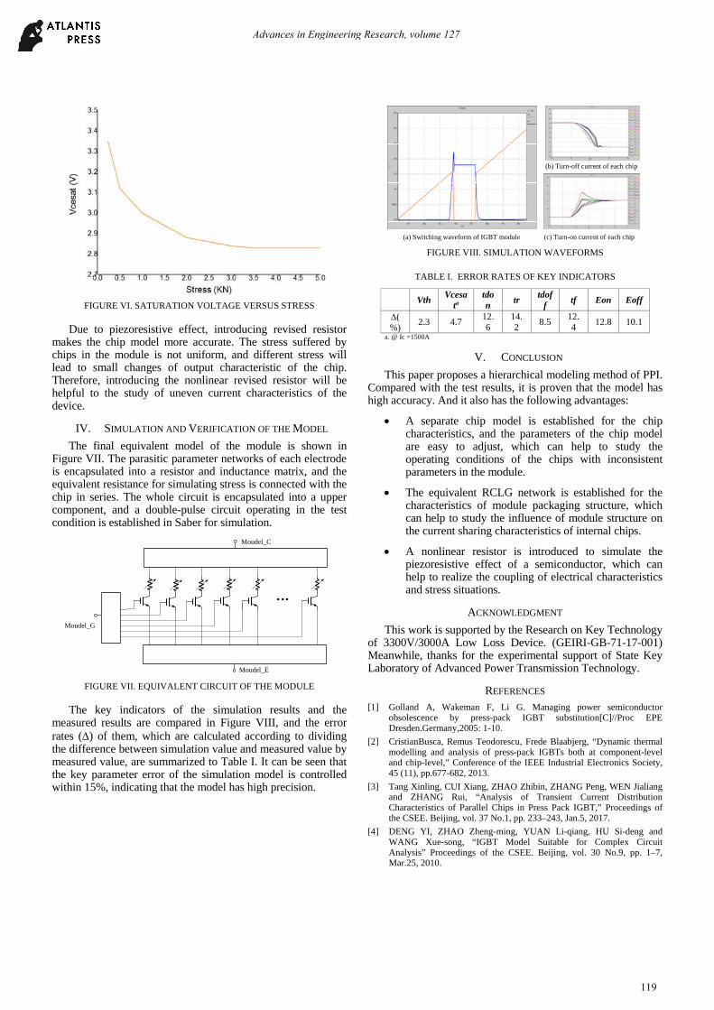
FIGURE VI. SATURATION VOLTAGE VERSUS STRESS
Due to piezoresistive effect, introducing revised resistor makes the chip model more accurate. The stress suffered by chips in the module is not uniform, and different stress will lead to small changes of output characteristic of the chip. Therefore, introducing the nonlinear revised resistor will be helpful to the study of uneven current characteristics of the device.
IV. SIMULATION AND VERIFICATION OF THE MODEL
The final equivalent model of the module is shown in Figure VII. The parasitic parameter networks of each electrode is encapsulated into a resistor and inductance matrix, and the equivalent resistance for simulating stress is connected with the chip in series. The whole circuit is encapsulated into a upper component, and a double-pulse circuit operating in the test condition is established in Saber for simulation.
Moudel_C
Moudel_E
Moudel_G
FIGURE VII. EQUIVALENT CIRCUIT OF THE MODULE
The key indicators of the simulation results and the measured results are compared in Figure VIII, and the error rates () of them, which are calculated according to dividing the difference between simulation value and measured value by measured value, are summarized to Table I. It can be seen that the key parameter error of the simulation model is controlled within 15%, indicating that the model has high precision.
(a) Switching waveform of IGBT module
(b) Turn-off current of each chip
(c) Turn-on current of each chip FIGURE VIII. SIMULATION WAVEFORMS
TABLE I. ERROR RATES OF KEY INDICATORS
Vth
Vcesata
tdon
tr tdof
f tf Eon Eoff
(%)
2.3 4.7 12.6
14.2
8.5 12.4
12.8 10.1
a. @ Ic =1500A
V. CONCLUSION
This paper proposes a hierarchical modeling method of PPI. Compared with the test results, it is proven that the model has high accuracy. And it also has the following advantages:
A separate chip model is established for the chip characteristics, and the parameters of the chip model are easy to adjust, which can help to study the operating conditions of the chips with inconsistent parameters in the module.
The equivalent RCLG network is established for the characteristics of module packaging structure, which can help to study the influence of module structure on the current sharing characteristics of internal chips.
A nonlinear resistor is introduced to simulate the piezoresistive effect of a semiconductor, which can help to realize the coupling of electrical characteristics and stress situations.
ACKNOWLEDGMENT
This work is supported by the Research on Key Technology of 3300V/3000A Low Loss Device. (GEIRI-GB-71-17-001) Meanwhile, thanks for the experimental support of State Key Laboratory of Advanced Power Transmission Technology.
REFERENCES [1] Golland A, Wakeman F, Li G. Managing power semiconductor
obsolescence by press-pack IGBT substitution[C]//Proc EPE Dresden.Germany,2005: 1-10.
[2] CristianBusca, Remus Teodorescu, Frede Blaabjerg, “Dynamic thermal modelling and analysis of press-pack IGBTs both at component-level and chip-level,” Conference of the IEEE Industrial Electronics Society, 45 (11), pp.677-682, 2013.
[3] Tang Xinling, CUI Xiang, ZHAO Zhibin, ZHANG Peng, WEN Jialiang and ZHANG Rui, “Analysis of Transient Current Distribution Characteristics of Parallel Chips in Press Pack IGBT,” Proceedings of the CSEE. Beijing, vol. 37 No.1, pp. 233–243, Jan.5, 2017.
[4] DENG YI, ZHAO Zheng-ming, YUAN Li-qiang, HU Si-deng and WANG Xue-song, “IGBT Model Suitable for Complex Circuit Analysis” Proceedings of the CSEE. Beijing, vol. 30 No.9, pp. 1–7, Mar.25, 2010.
Advances in Engineering Research, volume 127
119

[5] Allen R. Hefner, Daniel M. Diebolt, “An Expermentally Verified IGBT Model Implement in the Saber Curcuit Simulator,” IEEE Power Electronics Specialists Conference, 9 (5):10-19, 1991.
[6] Li Shengnan, Tolbert L M, Wang F, et al. “P-cell and N-cell based IGBT module: layout design, Parasitic extraction, and experimental verification,” Applied Power Electronics Conference & Exposition, pp.372-378, 2011.
[7] Yoshikazu Takahashi, Takeharu Koga, Humiaki Kirihata and Yasukazu Seki “2.5kV 100A -stack IGBT” International Symposium on Power Semiconductor Devices & Ics, 14 (2-3), pp.25-30, 1994.
Advances in Engineering Research, volume 127
120